Document Revision History Revision Date Description Changed by
0 12/15/2014 Initial Release AK
Functions and Features 2 lines x 20 characters
Built‐in LCD comparable controller
4/8‐bit Parallel, SPI, or I²C MPU interface
2.8V or 5.0V operation
RoHS compliant
Slim design
CONFI
DENTIA
L1 2 3 4 5 6
A
B
C
D
B
C
D
1 2 3 4 5 6
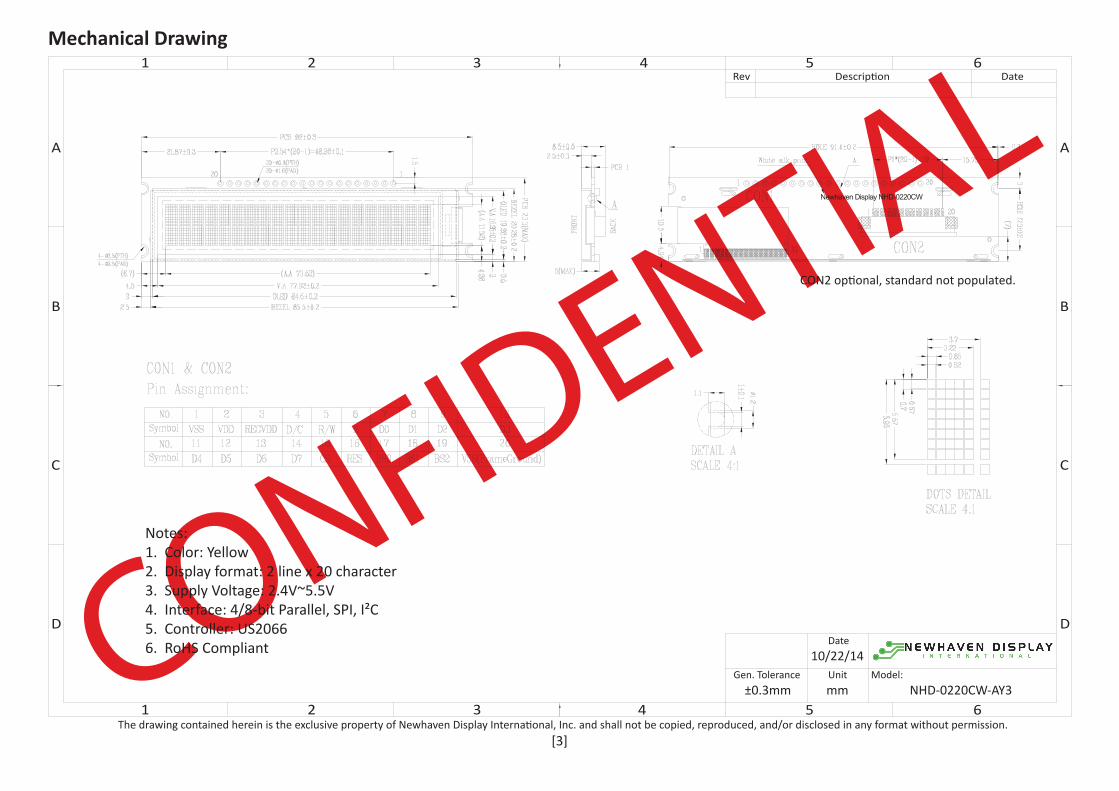
Mechanical Drawing
A
[3]The drawing contained herein is the exclusive property of Newhaven Display International, Inc. and shall not be copied, reproduced, and/or disclosed in any format without permission.
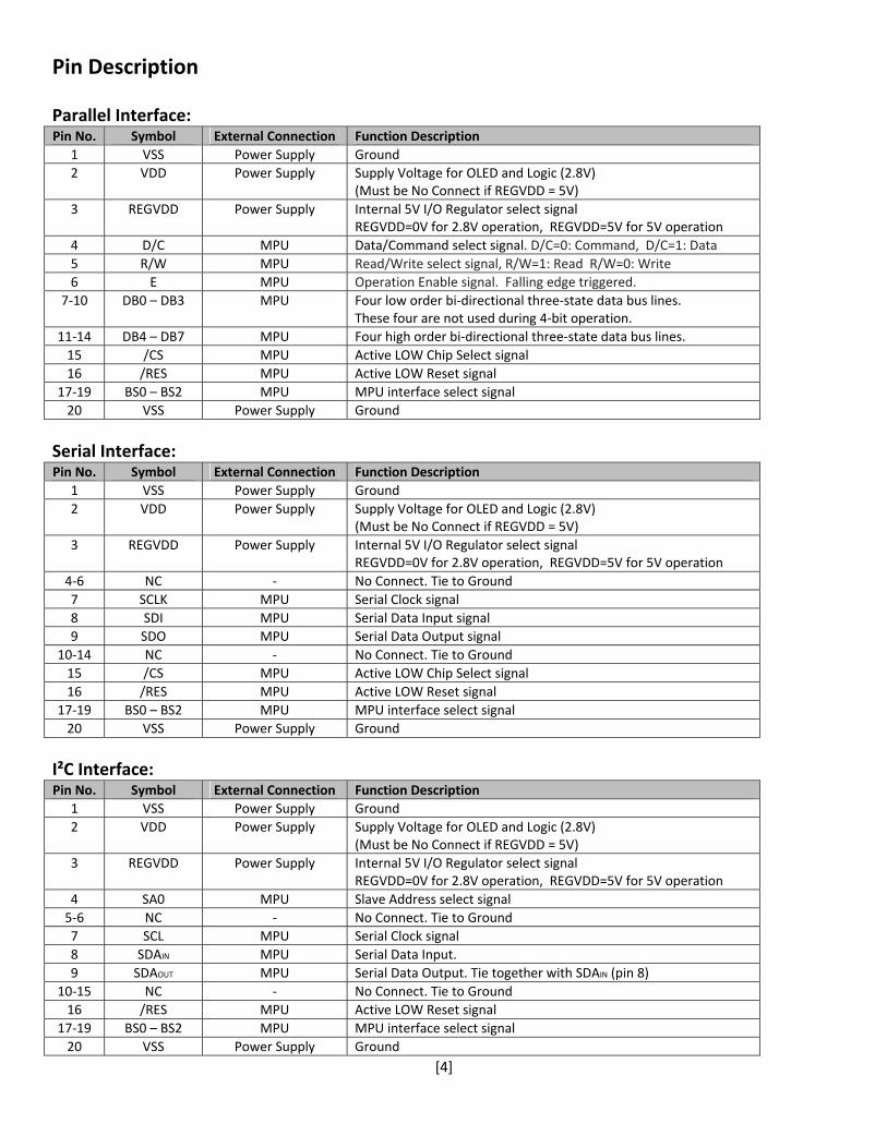
6 E MPU Operation Enable signal. Falling edge triggered.
7‐10 DB0 – DB3 MPU Four low order bi‐directional three‐state data bus lines. These four are not used during 4‐bit operation.
11‐14 DB4 – DB7 MPU Four high order bi‐directional three‐state data bus lines.
15 /CS MPU Active LOW Chip Select signal
16 /RES MPU Active LOW Reset signal
17‐19 BS0 – BS2 MPU MPU interface select signal
20 VSS Power Supply Ground
Serial Interface: Pin No. Symbol External Connection Function Description
1 VSS Power Supply Ground
2 VDD Power Supply Supply Voltage for OLED and Logic (2.8V)(Must be No Connect if REGVDD = 5V)
3 REGVDD Power Supply Internal 5V I/O Regulator select signalREGVDD=0V for 2.8V operation, REGVDD=5V for 5V operation
4‐6 NC ‐ No Connect. Tie to Ground
7 SCLK MPU Serial Clock signal
8 SDI MPU Serial Data Input signal
9 SDO MPU Serial Data Output signal
10‐14 NC ‐ No Connect. Tie to Ground
15 /CS MPU Active LOW Chip Select signal
16 /RES MPU Active LOW Reset signal
17‐19 BS0 – BS2 MPU MPU interface select signal
20 VSS Power Supply Ground
I²C Interface: Pin No. Symbol External Connection Function Description
1 VSS Power Supply Ground
2 VDD Power Supply Supply Voltage for OLED and Logic (2.8V)(Must be No Connect if REGVDD = 5V)
3 REGVDD Power Supply Internal 5V I/O Regulator select signalREGVDD=0V for 2.8V operation, REGVDD=5V for 5V operation
4 SA0 MPU Slave Address select signal
5‐6 NC ‐ No Connect. Tie to Ground
7 SCL MPU Serial Clock signal
8 SDAIN MPU Serial Data Input.
9 SDAOUT MPU Serial Data Output. Tie together with SDAIN (pin 8)
10‐15 NC ‐ No Connect. Tie to Ground
16 /RES MPU Active LOW Reset signal
17‐19 BS0 – BS2 MPU MPU interface select signal
20 VSS Power Supply Ground
[5]
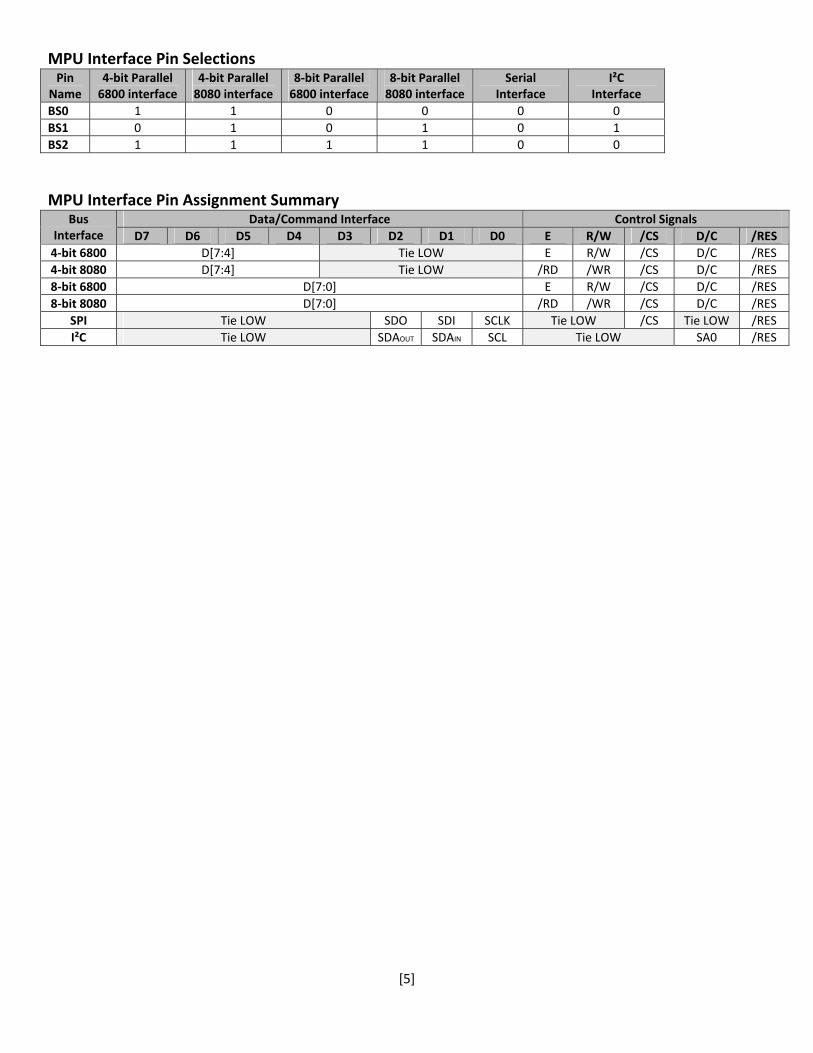
MPU Interface Pin Selections Pin
Name 4‐bit Parallel 6800 interface
4‐bit Parallel 8080 interface
8‐bit Parallel 6800 interface
8‐bit Parallel 8080 interface
Serial Interface
I²C Interface
BS0 1 1 0 0 0 0
BS1 0 1 0 1 0 1
BS2 1 1 1 1 0 0
MPU Interface Pin Assignment Summary Bus
Interface Data/Command Interface Control Signals
D7 D6 D5 D4 D3 D2 D1 D0 E R/W /CS D/C /RES
4‐bit 6800 D[7:4] Tie LOW E R/W /CS D/C /RES
4‐bit 8080 D[7:4] Tie LOW /RD /WR /CS D/C /RES
8‐bit 6800 D[7:0] E R/W /CS D/C /RES
8‐bit 8080 D[7:0] /RD /WR /CS D/C /RES
SPI Tie LOW SDO SDI SCLK Tie LOW /CS Tie LOW /RES
I²C Tie LOW SDAOUT SDAIN SCL Tie LOW SA0 /RES
[6]
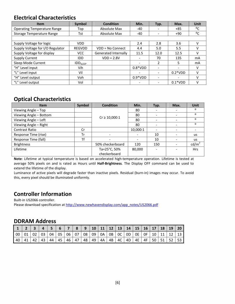
Electrical Characteristics Item Symbol Condition Min. Typ. Max. Unit
Operating Temperature Range Top Absolute Max ‐40 ‐ +85 ⁰C
Storage Temperature Range Tst Absolute Max ‐40 ‐ +90 ⁰C
Supply Voltage for logic VDD 2.4 2.8 3.6 V
Supply Voltage for I/O Regulator REGVDD VDD = No Connect 4.4 5.0 5.5 V
Supply Voltage for display VCC Generated Internally 11.5 12.0 12.5 V
Supply Current IDD VDD = 2.8V ‐ 70 135 mA
Sleep Mode Current IDDSLEEP ‐ 2 5 mA
“H” Level input Vih 0.8*VDD ‐ ‐ V
“L” Level input Vil ‐ ‐ 0.2*VDD V
“H” Level output Voh 0.9*VDD ‐ ‐ V
“L” Level output Vol ‐ ‐ 0.1*VDD V
Optical Characteristics Item Symbol Condition Min. Typ. Max. Unit
Viewing Angle – Top
Cr ≥ 10,000:1
80 ‐ ‐ ⁰
Viewing Angle – Bottom 80 ‐ ‐ ⁰
Viewing Angle – Left 80 ‐ ‐ ⁰
Viewing Angle – Right 80 ‐ ‐ ⁰
Contrast Ratio Cr 10,000:1 ‐ ‐ ‐
Response Time (rise) Tr ‐ ‐ 10 ‐ us
Response Time (fall) Tf ‐ ‐ 10 ‐ us
Brightness 50% checkerboard 120 150 ‐ cd/m2
Lifetime Ta=25°C, 50% checkerboard
80,000 ‐ ‐ Hrs
Note: Lifetime at typical temperature is based on accelerated high‐temperature operation. Lifetime is tested at average 50% pixels on and is rated as Hours until Half‐Brightness. The Display OFF command can be used to extend the lifetime of the display. Luminance of active pixels will degrade faster than inactive pixels. Residual (burn‐in) images may occur. To avoid this, every pixel should be illuminated uniformly.
Controller Information Built‐in US2066 controller. Please download specification at http://www.newhavendisplay.com/app_notes/US2066.pdf
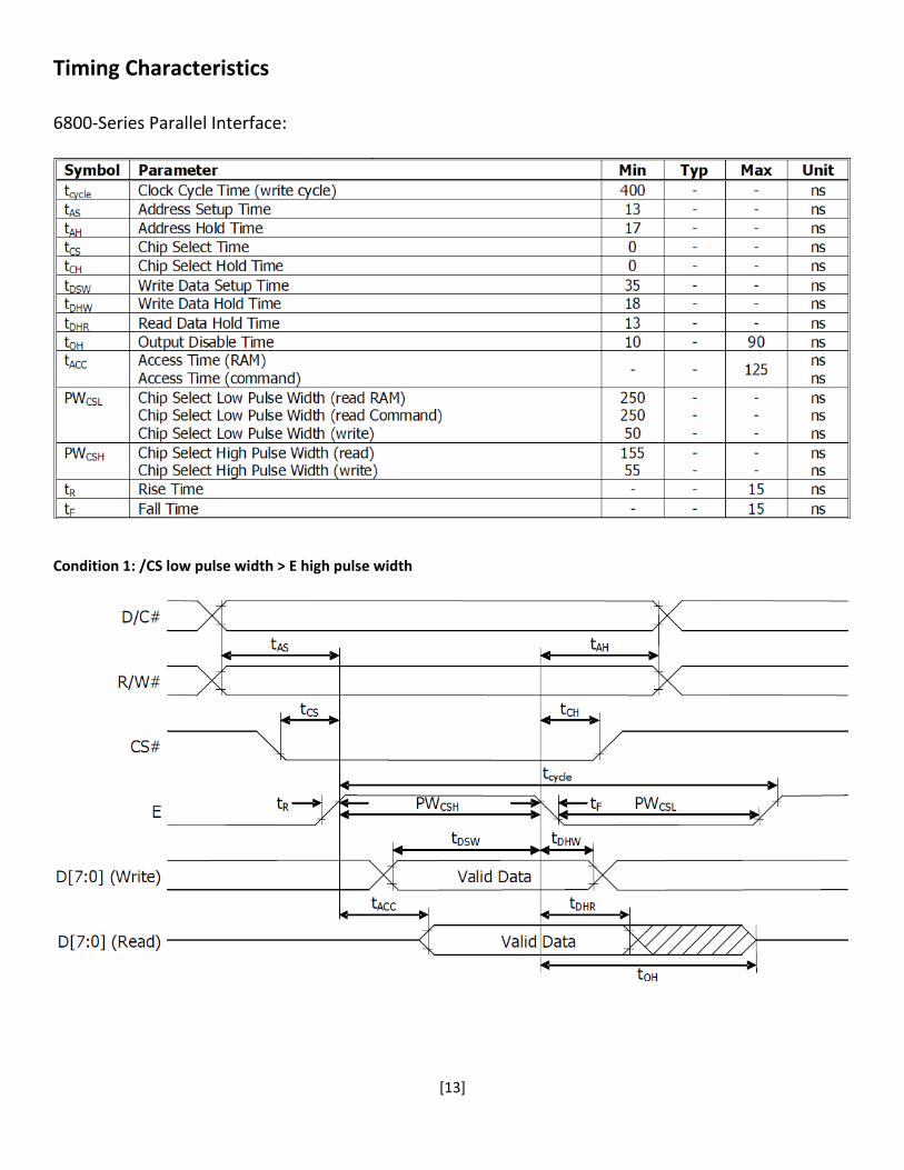
Condition 1: /CS low pulse width > E high pulse width
[14]
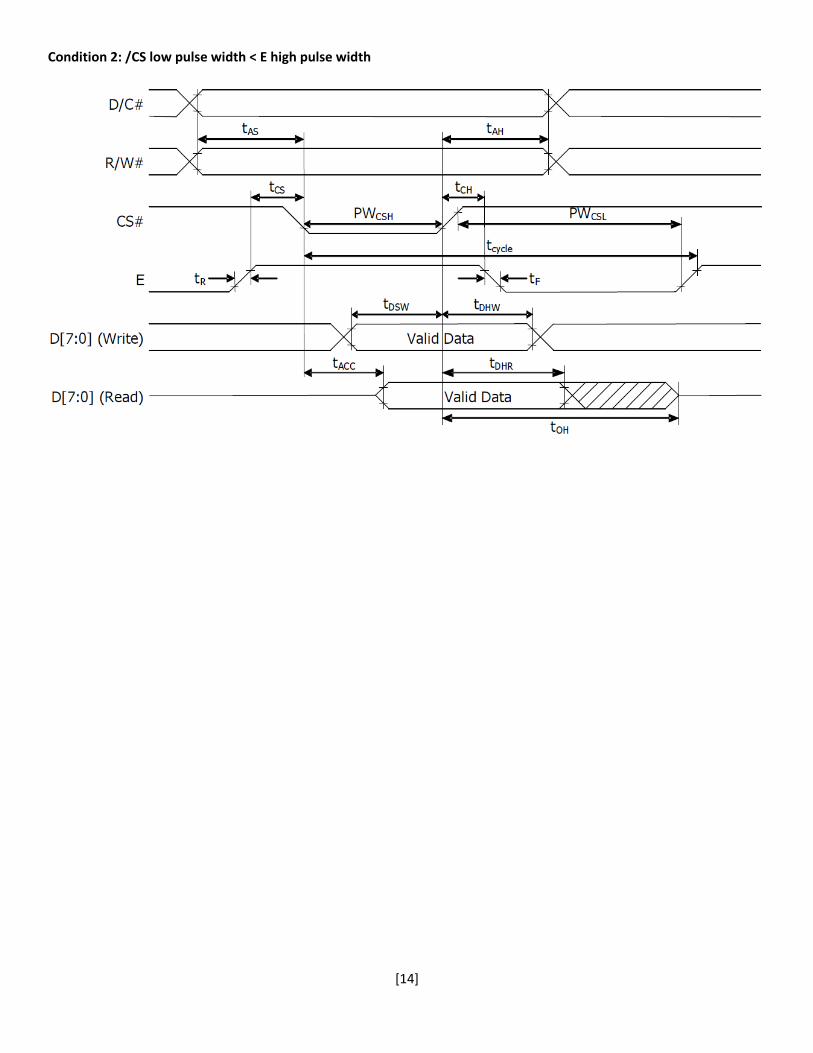
Condition 2: /CS low pulse width < E high pulse width
[15]
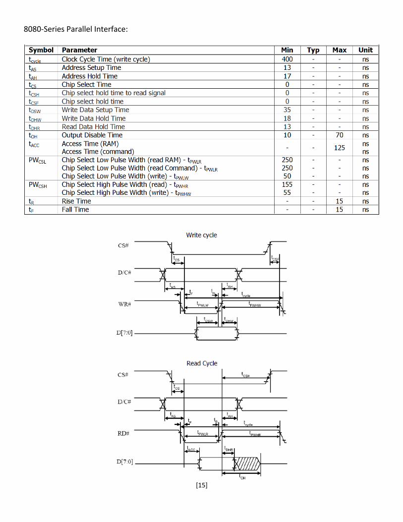
8080‐Series Parallel Interface:
[16]
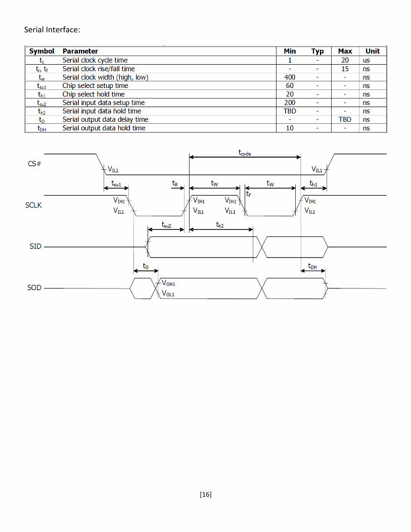
Serial Interface:
[17]
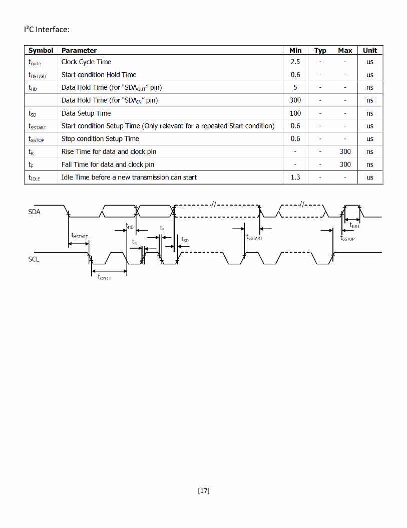
I²C Interface:
[18]
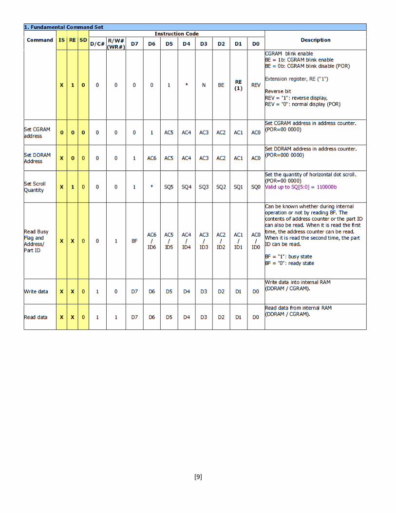
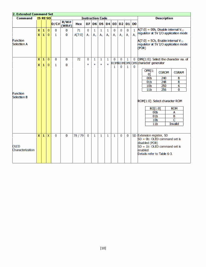
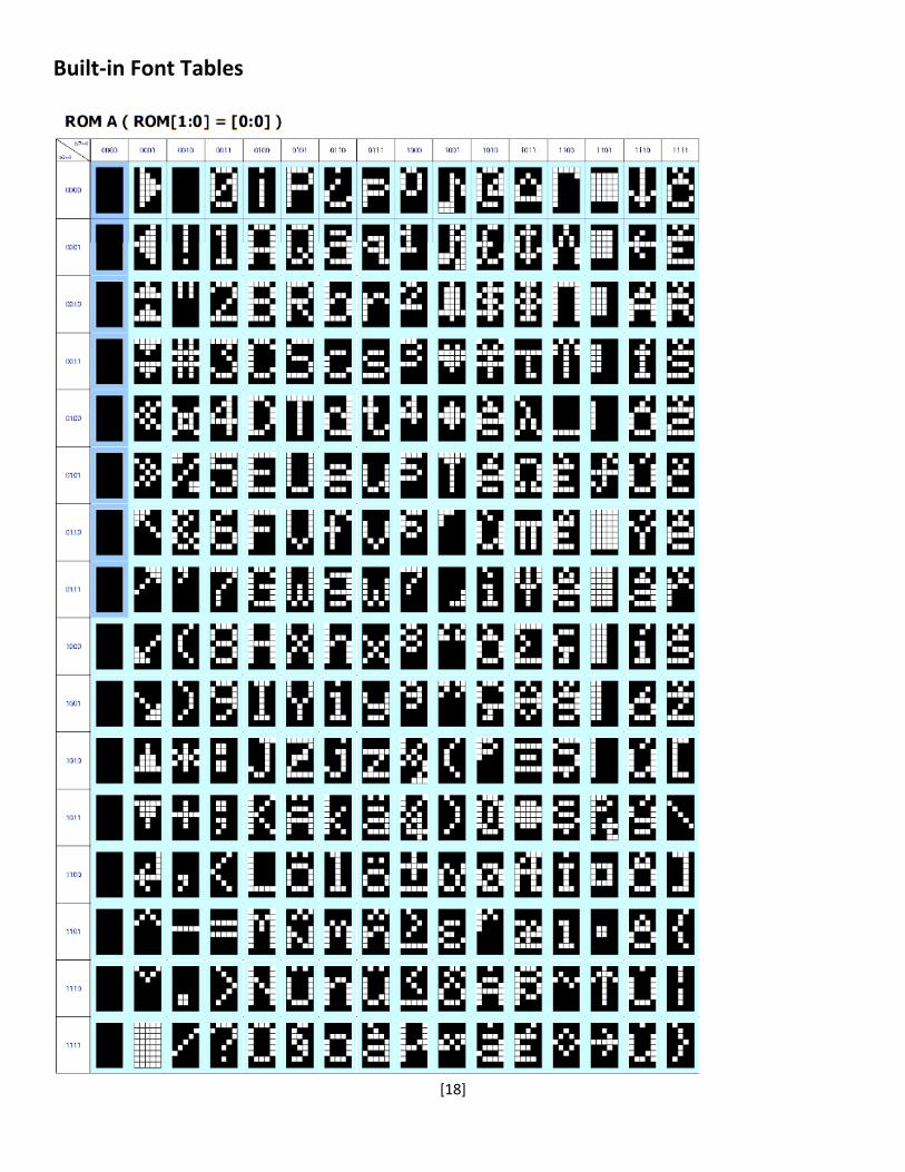
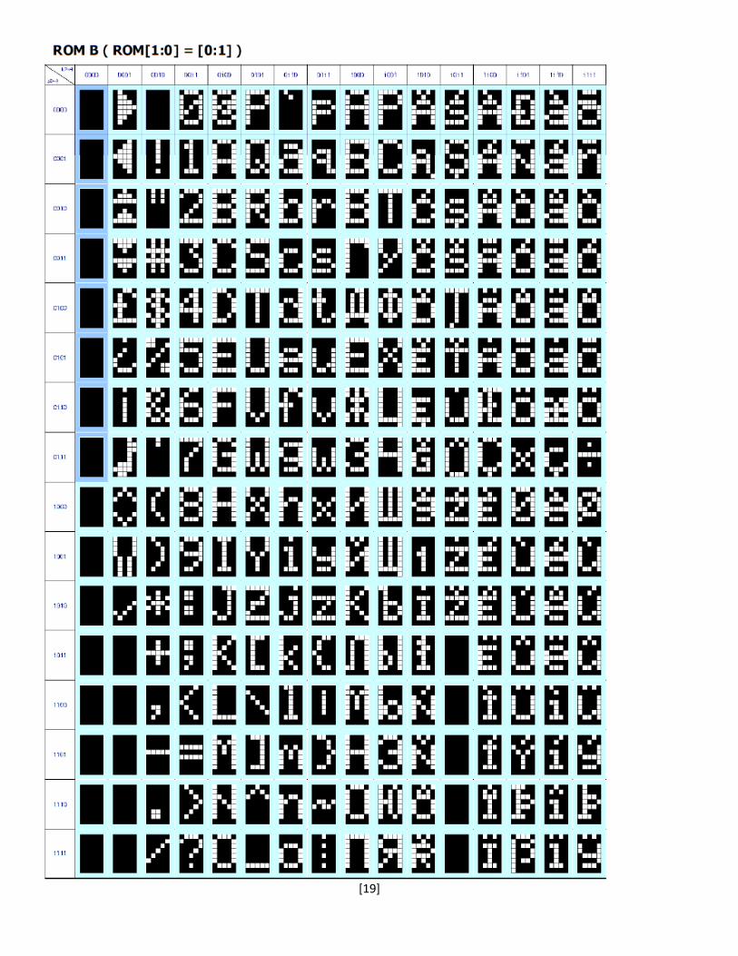
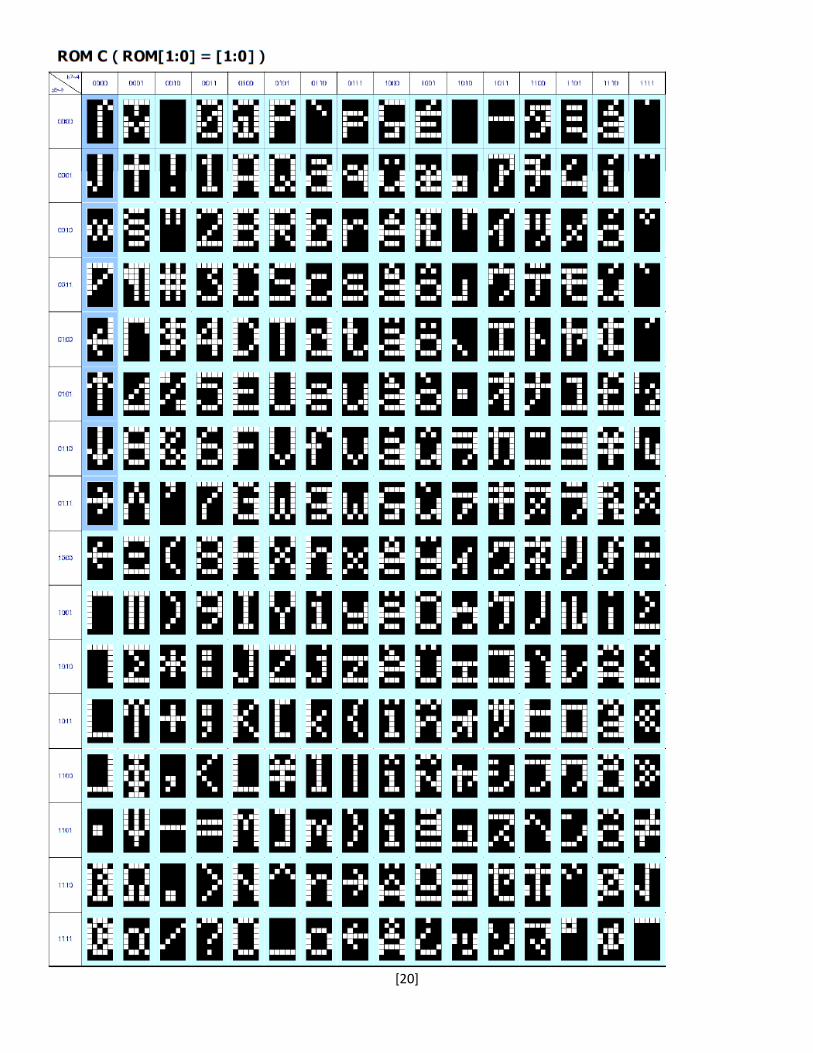
Built‐in Font Tables
[19]
[20]
[21]
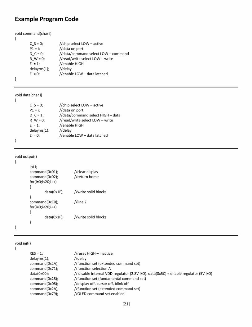
Example Program Code void command(char i) {
C_S = 0; //chip select LOW – active P1 = i; //data on port D_C = 0; //data/command select LOW – command R_W = 0; //read/write select LOW – write E = 1; //enable HIGH delayms(1); //delay E = 0; //enable LOW – data latched
}
void data(char i) {
C_S = 0; //chip select LOW – active P1 = i; //data on port D_C = 1; //data/command select HIGH – data R_W = 0; //read/write select LOW – write E = 1; //enable HIGH delayms(1); //delay E = 0; //enable LOW – data latched
}
void output() {
int i; command(0x01); //clear display command(0x02); //return home for(i=0;i<20;i++) {
delayms(1); //delay command(0x2A); //function set (extended command set)
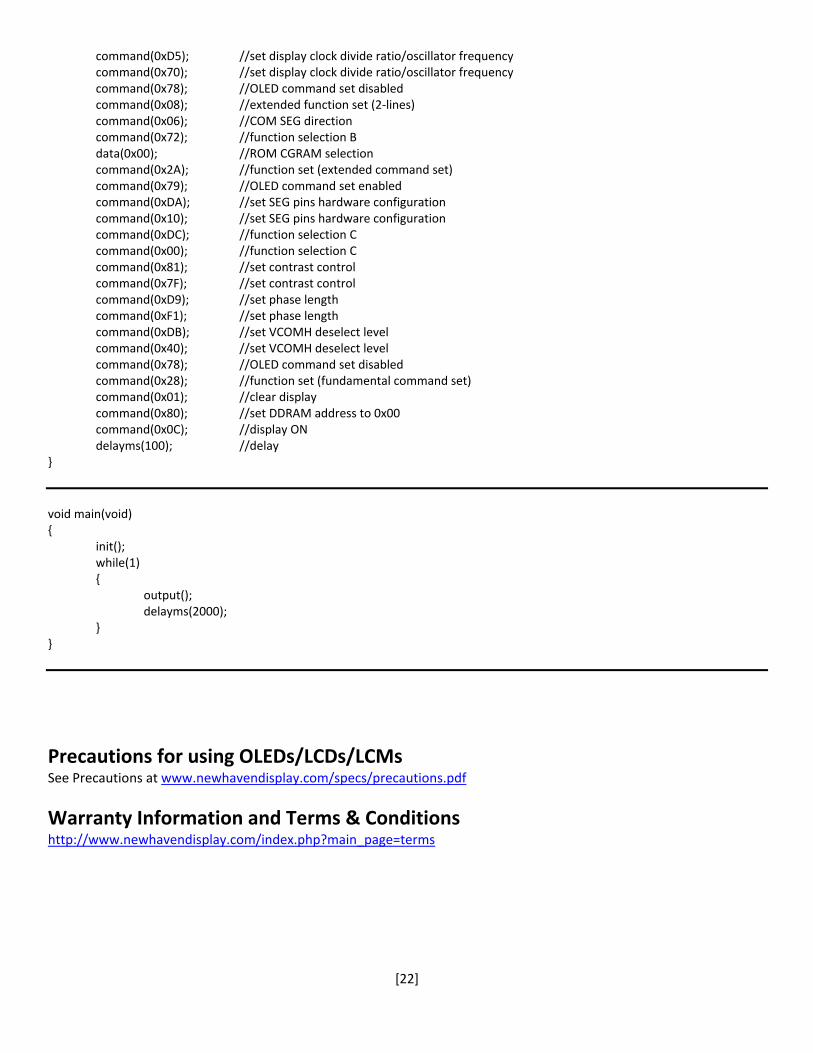
command(0x71); //function selection A data(0x00); // disable internal VDD regulator (2.8V I/O). data(0x5C) = enable regulator (5V I/O) command(0x28); //function set (fundamental command set) command(0x08); //display off, cursor off, blink off command(0x2A); //function set (extended command set) command(0x79); //OLED command set enabled
[22]
command(0xD5); //set display clock divide ratio/oscillator frequency command(0x70); //set display clock divide ratio/oscillator frequency command(0x78); //OLED command set disabled command(0x08); //extended function set (2‐lines)
command(0x06); //COM SEG direction command(0x72); //function selection B data(0x00); //ROM CGRAM selection command(0x2A); //function set (extended command set) command(0x79); //OLED command set enabled command(0xDA); //set SEG pins hardware configuration command(0x10); //set SEG pins hardware configuration command(0xDC); //function selection C command(0x00); //function selection C command(0x81); //set contrast control command(0x7F); //set contrast control command(0xD9); //set phase length command(0xF1); //set phase length command(0xDB); //set VCOMH deselect level command(0x40); //set VCOMH deselect level command(0x78); //OLED command set disabled command(0x28); //function set (fundamental command set) command(0x01); //clear display command(0x80); //set DDRAM address to 0x00 command(0x0C); //display ON
delayms(100); //delay }
void main(void) {
init(); while(1) {
output(); delayms(2000);
} }
Precautions for using OLEDs/LCDs/LCMs See Precautions at www.newhavendisplay.com/specs/precautions.pdf
Warranty Information and Terms & Conditions http://www.newhavendisplay.com/index.php?main_page=terms