NI PXI/PCI-6561/6562 Specifications 100/200 MHz Digital Waveform Generator/Analyzer This document provides the specifications for the NI PXI/PCI-6561 (NI 6561) and the NI PXI/PCI-6562 (NI 6562), collectively called the NI 656x. Typical values are representative of an average unit operating at room temperature. Specifications are subject to change without notice. For the most recent NI 656x specifications, visit ni.com/manuals. To access the NI 656x documentation, including the NI Digital Waveform Generator/Analyzer Getting Started Guide, which contains functional descriptions of the NI 656x signals, navigate to Start»All Programs» National Instruments»NI-HSDIO»Documentation. Caution If the NI 656x has been in use, it may exceed safe handling temperatures and cause burns. Allow the NI 656x to cool before removing it from the chassis. Contents Channel Specifications ............................................................................ 2 Generation Channels (Data, DDC CLK OUT, and PFI <0..3>) ...... 3 Acquisition Channels (Data, STROBE, and PFI <0..3>) ................ 4 Timing Specifications ............................................................................. 5 Sample Clock ................................................................................... 5 Generation Timing (Data, DDC CLK OUT, and PFI <0..3> Channels) ............................................................. 7 Acquisition Timing (Data, STROBE, and PFI <0..3> Channels).... 12 CLK IN (SMB Jack Connector) ...................................................... 16 STROBE (DDC Connector) ............................................................ 17 PXI_STAR (PXI Backplane) ........................................................... 18 CLK OUT (SMB Jack Connector) .................................................. 18 DDC CLK OUT LVDS (DDC Connector)...................................... 19 DDC CLK OUT LVPECL (DDC Connector) ................................. 19 Reference Clock (PLL) .................................................................... 20
Transcript
NI PXI/PCI-6561/6562 Specifications100/200 MHz Digital Waveform Generator/Analyzer
This document provides the specifications for the NI PXI/PCI-6561 (NI 6561) and the NI PXI/PCI-6562 (NI 6562), collectively called the NI 656x.
Typical values are representative of an average unit operating at room temperature. Specifications are subject to change without notice. For the most recent NI 656x specifications, visit ni.com/manuals.
To access the NI 656x documentation, including the NI Digital Waveform Generator/Analyzer Getting Started Guide, which contains functional descriptions of the NI 656x signals, navigate to Start»All Programs»National Instruments»NI-HSDIO»Documentation.
Caution If the NI 656x has been in use, it may exceed safe handling temperatures and cause burns. Allow the NI 656x to cool before removing it from the chassis.
and PFI <0..3> Channels) ............................................................. 7Acquisition Timing (Data, STROBE, and PFI <0..3> Channels).... 12CLK IN (SMB Jack Connector) ...................................................... 16STROBE (DDC Connector) ............................................................ 17PXI_STAR (PXI Backplane)........................................................... 18CLK OUT (SMB Jack Connector) .................................................. 18DDC CLK OUT LVDS (DDC Connector)...................................... 19DDC CLK OUT LVPECL (DDC Connector) ................................. 19Reference Clock (PLL) .................................................................... 20
NI PXI/PCI-6561/6562 Specifications 2 ni.com
Waveform Specifications ........................................................................21Memory and Scripting......................................................................21Triggers (Inputs to the NI 656x).......................................................23Events (Generated from the NI 656x) ..............................................25Miscellaneous ...................................................................................26Power................................................................................................26Software............................................................................................27Environment .....................................................................................28Safety, Electromagnetic Compatibility, and CE Compliance ..........29Physical Specifications.....................................................................30
Channel Specifications
Specification Value Comments
Number of data channels
16 —
Direction control of data channels
Single Data Rate (SDR) Double Data Rate (DDR) Using SDR, data is clocked using the rising or falling edge of the Sample clock. Using DDR, data is clocked using both edges of the Sample clock.
Data<0..15> Per channel Data<0..7> Dedicated for data generation
Data<8..15> Dedicated for data acquisition
Number of Programmable Function Interface (PFI) channels
4 Refer to the Waveform Specifications section for more details.
Direction control of PFI channels
Per channel —
Number of clock terminals
3 input3 output
Refer to the Timing Specifications section for more details.
Generation Channels (Data, DDC CLK OUT, and PFI <0..3>)
Specification Value Comments
Generation voltage families
Data <0..15>, PFI <1..2>, DDC CLK OUT LVDS
DDC CLK OUT
LVPECL PFI 0 PFI 3
—
LVDS LVPECL LVCMOS LVDS or LVCMOS (software selectable)
Generation voltage levels (LVDS)
Offset (Vos) Differential Voltage (Vod) Into 100 Ω differential load, TIA/EIA-644 compliant
Min Typ Max Min Typ Max
1.125 V 1.220 V 1.375 V 247 mV 305 mV 454 mV
Generation voltage levels (LVCMOS)
Low Voltage Levels High Voltage Levels —
Max Min
0.2 V 2.8 V
Generation voltage levels (LVPECL)
Single Ended Output High Single Ended Output Low Into open load.
Min Max Min Max
2.16 V 2.50 V 1.38 V 1.72 V
Output impedance
LVDS LVCMOS/LVPECL Nominal
100 Ω differential 50 Ω series
Data channel driver enable/disable control
Per channel Software-selectable
Channel power-on state
Drivers disabled, 100 Ω differential impedance
Data channels have a weak pull-up resistor (300 kΩ), internal to the I/0 buffer, to 3.3 V. This internal pull-up resistor is a fail-safe mechanism intended to set a known state when the receiver circuit is not being driven.
PFI 3 powers up in LVDS mode.
Output protection
Each channel can indefinitely sustain a short to any voltage between 0 and 5 V and is protected from up to 12 kV ESD.
—
NI PXI/PCI-6561/6562 Specifications 4 ni.com
Acquisition Channels (Data, STROBE, and PFI <0..3>)
Specification Value Comments
Acquisition voltage families
Data <0..15>, PFI <1..2> and STROBE PFI 0 PFI 3
—
LVDS LVCMOS LVDS or LVCMOS (software-selectable)
Acquisition voltage levels (LVDS)
Voltage Threshold Voltage Range TIA/EIA-644 compliant
Max1 Min Max
±50 mV 0 V 2.4 V
Acquisition voltage levels (LVCMOS)
Low Voltage Threshold High Voltage Threshold —
Max Min
0.8 V 2 V
Input impedance
LVDS LVCMOS PFI 3 powers up in LVDS mode.100 Ω differential 10 kΩ
Data channels have a weak pull-up resistor (300 kΩ), internal to the I/O buffer, to 3.3 V. This internal pull-up resistor is a fail-safe mechanism intended to set a known state when the receiver circuit is not being driven.
Input protection
Each channel can indefinitely sustain a short to any voltage between 0 and 5 V and is protected from up to 12 kV ESD.
—
1 The device under test must supply more than 50 mV of differential voltage.
1 ns maximumTransition time could be as fast as 610 ps.
20 to 80% transitions.
PFI transition time PFI 0 PFI <1..2>
PFI 3 (LVCMOS) PFI 3 (LVDS)
Typical.20 to 80% transitions.
6 ns 2.5 ns 6 ns 4.2 ns
Exported Sample clock offset (tCO)
1.6 ns Refer to Figure 3, Generation Provided Setup and Hold Times Timing Diagram.
Time delay from internal Sample clock to DDC Connector (tSCDDC)
5.8 ns Typical.
Exported Sample clock offset to selectable PFI
LVDS (tCPD) LVCMOS (tCPS) Typical.
2 ns 3.45 ns
Generation provided setup and hold times
Minimum Provided Setup Time (tSUP)
Minimum Provided Hold Time (tHP)
Exported Sample clock mode set to Noninverted.tp – 2.2 ns 1.1 ns
Compare the setup and hold times from the datasheet of your device under test (DUT) to the values in the preceding table. The provided setup and hold times must be greater than the setup and hold times required for the DUT. If you require more setup time, configure your exported Sample clock mode as Inverted and/or delay your data relative to the Sample clock.
Refer to Figure 3, Generation Provided Setup and Hold Times Timing Diagram, for a diagram illustrating the relationship between the exported Sample clock mode and the provided setup and hold times.
Notes: This table assumes the Data Position is set to the rising edge of the Sample clock and that the Sample clock is exported to the DDC connector.
This table includes worst-case effects of channel-to-channel skew, inter-symbol interference, and jitter.
NI PXI/PCI-6561/6562 Specifications 10 ni.com
Figure 3. Generation Provided Setup and Hold Times Timing Diagram
tPSU (SDR)
tPSU (DDR)
tCO
tP
ExportedSample Clock
DATA CHANNELS
Data PositionRising Edge
(Noninverted Clock, tCO = 1.6 ns)
tPH
tP = = Period of Sample Clock
tPH = Minimum Provided Hold Time
tPSU = Minimum Provided Setup Time; SDR = Single Data Rate, DDR = Double Data Rate
tCO = Exported Sample Clock Offset
Note: At 25 MHz and higher, STROBE duty cycle is corrected to 50%.
NI 6562: 40 to 60% for clock frequencies ≥50 MHz25 to 75% for clock frequencies <50 MHz
—
Minimum detectable pulse width
2 ns —
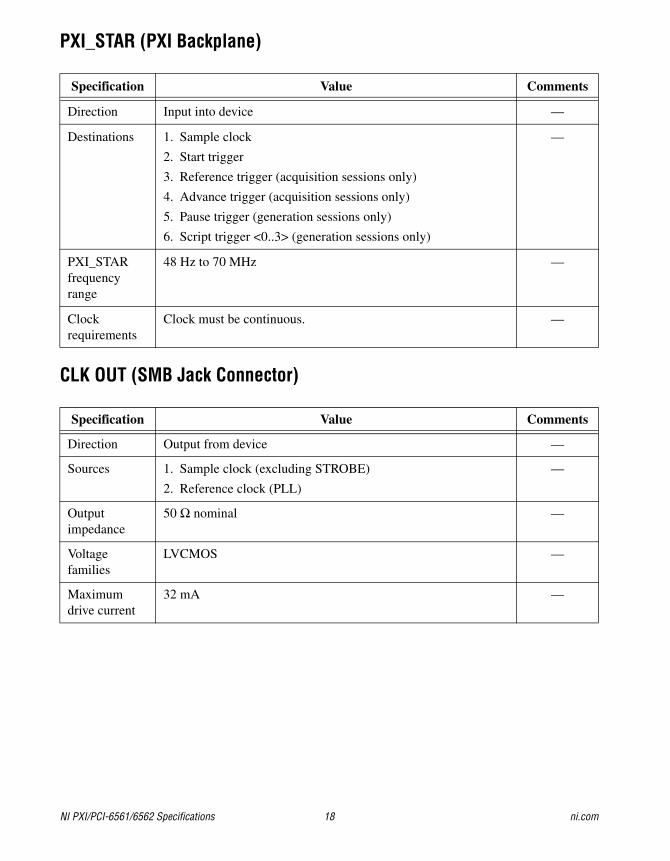
Clock requirements
Clock must be continuous. —
Input impedance
100 Ω differential
Data channels have a weak pull-up resistor (300 kΩ), internal to the I/O buffer, to 3.3 V. This internal pull-up resistor is a fail-safe mechanism intended to set a known state when the receiver circuit is not being driven.
Note: Exporting the internal Sample clock to DDC CLK OUT in software will export the internal Sample clock to the DDC CLK OUT LVDS and DDC CLK OUT LVPECL terminals.
STROBE cannot be routed to DDC CLKOUT.
Voltage families
LVDS —
Voltage levels
Offset (Vos) Differential Voltage (Vod) Into 100 Ω differential load,TIA/EIA-644 compliant
Min Typ Max Min Typ Max
1.125 V 1.220 V 1.375 V 247 mV 305 mV 454 mV
Transition time
1 ns —
Output impedance
100 Ω differential —
Output protection
This terminal can indefinitely sustain a short to any voltage between 0 and 5 V and is protected from up to 15 kV ESD.
—
Specification Value Comments
Direction Output from device —
Source Sample clock
Note: Exporting the internal Sample clock to DDC CLK OUT in software will export the internal Sample clock to the DDC CLK OUT LVDS and DDC CLK OUT LVPECL terminals.
STROBE cannot be routed to DDC CLKOUT.
Voltage families
LVPECL —
Voltage levels Single-Ended Output High Single-Ended Output Low Into open load
Min Max Min Max
2.16 V 2.50 V 1.38 V 1.72 V
NI PXI/PCI-6561/6562 Specifications 20 ni.com
Reference Clock (PLL)
Transition time
1 ns —
Output impedance
50 Ω source series nominal Series impedance on each polarity
Output protection
This terminal can indefinitely sustain a short to any voltage between 0 and 5 V and is protected from up to 15 kV ESD.
—
Specification Value Comments
Reference clock sources
1. PXI_CLK10 (PXI backplane—PXI only)
2. RTSI 7 (PCI only)
3. CLK IN (SMB jack connector)
4. None (onboard clock source not locked to a reference)
Provides the reference frequency for the phase lock loop
The NI 656x uses the Synchronization and Memory Core (SMC) technology in which waveforms and instructions share onboard memory. Parameters such as number of script instructions, maximum number of waveforms in memory, and number of samples (S) available for waveform storage are flexible and user-defined.
Refer to the Onboard Memory section in the NI Digital Waveform Generator/Analyzer Help for more information.
Onboard memory size
2 Mbit/channel (for generation sessions)
2 Mbit/channel (for acquisition sessions)
16 Mbit/channel (for generation sessions)
16 Mbit/channel (for acquisition sessions)
128 Mbit/channel (for generation sessions)
128 Mbit/channel (for acquisition sessions)
Maximum limit for generation sessions assumes no scripting instructions. Onboard memory size doubles with 8-bit data width (DDR mode).
Generation modes
Single-waveform mode:Generate a single waveform once, n times, or continuously.
—
Scripted mode:Generate a simple or complex sequence of waveforms. Use scripts to describe the waveforms to be generated, the order in which the waveforms are generated, how many times the waveforms are generated, and how the device responds to Script triggers.
1. Start trigger (edge detection: rising or falling)
2. Pause trigger (level detection: high or low)
3. Script trigger <0..3> (edge detection: rising or falling; level detection: high or low)
4. Reference trigger (edge detection: rising or falling)
5. Advance trigger (edge detection: rising or falling)
—
Minimum required trigger pulse width
Generation Triggers Acquisition Triggers
30 ns Acquisition triggers must meet setup and hold time requirements.
For triggers synchronous to STROBE, triggers must meet setup and hold requirements. For asynchronous triggers, pulse width must be larger than the greater of 30 ns or Clock Period + Setup + Hold
NI-HSDIO driver software 1.3 or later. NI-HSDIO allows you to configure and control the NI 656x. NI-HSDIO provides application interfaces for many development environments. NI-HSDIO follows IVI application programming interface (API) guidelines.
—
Application software
NI-HSDIO provides programming interfaces for the following application development environments:
• National Instruments LabVIEW 7.0 or later
• National Instruments LabWindows™/CVI™ 6.0 or later
• Microsoft Visual C/C++ 6.0 or later
—
Test panel National Instruments Measurement & Automation Explorer (MAX) provides test panels with basic acquisition and generation functionality for the NI 656x. MAX is included on the NI-HSDIO driver CD.
—
NI PXI/PCI-6561/6562 Specifications 28 ni.com
Environment
Note To ensure that the NI 656x cools effectively, follow the guidelines in the Maintain Forced Air Cooling Note to Users included with the NI 656x. The NI 656x is intended for indoor use only.
Specification Value Comments
Operating temperature
PXI: 0 to +55 ºC in all NI PXI chassis except the following:
0 to +45 ºC when installed in an NI PXI-1000/B and NI PXI-101X chassis (Meets IEC 60068-2-1 and IEC 60068-2-2.)
PCI: 0 to +45 ºC
—
Storage temperature
–20 to 70 ºC —
Operating relative humidity
10 to 90% relative humidity, noncondensing (Meets IEC 60068-2-56)
—
Storage relative humidity
5 to 95% relative humidity, noncondensing (Meets IEC 60068-2-56)
—
Operating shock
30 g, half-sine, 11 ms pulse (Meets IEC 60068-2-27. Test profile developed in accordance with MIL-PRF-28800F.)
—
Storage shock
50 g, half-size, 11 ms pulse (Meets IEC 60068-2-27. Test profile developed in accordance with MIL-PRF-28800F.)
—
Operating vibration
5 to 500 Hz, 0.31 grms (Meets IEC 60068-2-64.) —
Storage vibration
5 to 500 Hz, 2.46 grms (Meets IEC 60068-2-64. Test profile exceeds requirements of MIL-PRF-28800F, Class 3.)
—
Maximum altitude
0 to 2,000 m above sea level (at 25 ºC ambient temperature) —
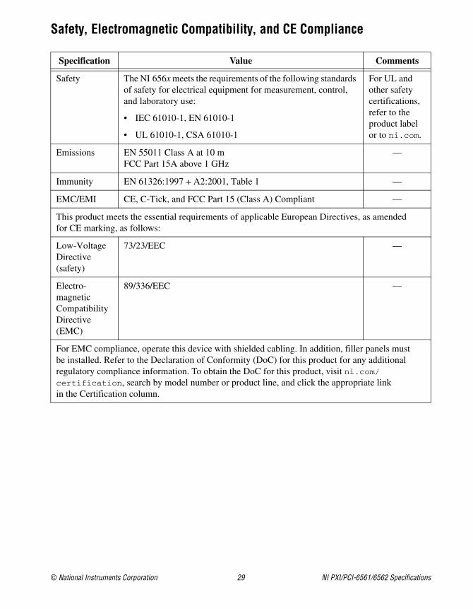
Safety, Electromagnetic Compatibility, and CE Compliance
Specification Value Comments
Safety The NI 656x meets the requirements of the following standards of safety for electrical equipment for measurement, control, and laboratory use:
• IEC 61010-1, EN 61010-1
• UL 61010-1, CSA 61010-1
For UL and other safety certifications, refer to the product label or to ni.com.
Emissions EN 55011 Class A at 10 mFCC Part 15A above 1 GHz
—
Immunity EN 61326:1997 + A2:2001, Table 1 —
EMC/EMI CE, C-Tick, and FCC Part 15 (Class A) Compliant —
This product meets the essential requirements of applicable European Directives, as amended for CE marking, as follows:
Low-Voltage Directive (safety)
73/23/EEC —
Electro-magnetic CompatibilityDirective (EMC)
89/336/EEC —
For EMC compliance, operate this device with shielded cabling. In addition, filler panels mustbe installed. Refer to the Declaration of Conformity (DoC) for this product for any additional regulatory compliance information. To obtain the DoC for this product, visit ni.com/certification, search by model number or product line, and click the appropriate linkin the Certification column.
NI PXI/PCI-6561/6562 Specifications 30 ni.com
Physical Specifications
Specification Value Comments
Dimensions PXI: 3U, One Slot, PXI/cPCI Module21.6 × 2.0 × 13.0 cm (8.5 × 0.8 × 5.1 in)
PCI: 12.6 × 35.5 cm (4.96 × 13.9 in.)
—
Weight PXI: 340 g (12 oz)
PCI: 410 g (14.5 oz)
—
Front Panel Connectors
Label Function(s) Connector Type —
CLK IN External Sample clock, external PLL reference input
SMB jack connector —
PFI 0 Events, triggers SMB jack connector —
CLK OUT Exported Sample clock, exported Reference clock
SMB jack connector —
DIGITAL DATA & CONTROL
Digital data channels, exported Sample clock, STROBE, events, triggers
12X InfiniBand connector —
Note: The NI SHB12X-B12X LVDS cable (192344-01) is a pass-through cable. When designing a custom fixture, notice that the cable pinout is reversed from that of the NI 656x. For example, the NI 656x generates DIO 0 on pin 14. This signal connects to pin 60 at the cable end. Refer to the NI Digital Waveform Generator/Analyzer Getting Started Guide or the NI Digital Waveform Generator/Analyzer Help for more pinout information.
National Instruments, NI, ni.com, and LabVIEW are trademarks of National Instruments Corporation. Refer to the Terms of Use section on ni.com/legal for more information about National Instruments trademarks. Other product and company names mentioned herein are trademarks or trade names of their respective companies. For patents covering National Instruments products, refer to the appropriate location: Help»Patents in your software, the patents.txt file on your CD, or ni.com/patents.