Page 1
Nicolo de Groot, Rutherford Appleton Laboratory DESY PRC, 7/8 May 2003 p. 1
CCD-based Vertex Detector - LCFI status report
Nicolo de Groot
RAL/Bristol
Conceptual design and goals
Detector R&D program at LCFI
Development of Column Parallel CCDs and readout electronics
Thin ladder program for mechanical support of the sensors
Physics design studies
Summary
CCD-based Vertex Detector
Page 2
Nicolo de Groot, Rutherford Appleton Laboratory DESY PRC, 7/8 May 2003 p. 2
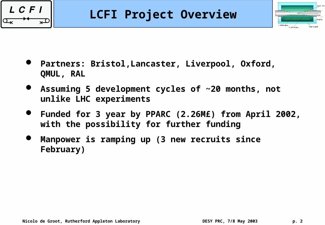
Partners: Bristol,Lancaster, Liverpool, Oxford, QMUL, RAL
Assuming 5 development cycles of ~20 months, not unlike LHC experiments
Funded for 3 year by PPARC (2.26M£) from April 2002, with the possibility for further funding
Manpower is ramping up (3 new recruits since February)
LCFI Project Overview
Page 3
Nicolo de Groot, Rutherford Appleton Laboratory DESY PRC, 7/8 May 2003 p. 3
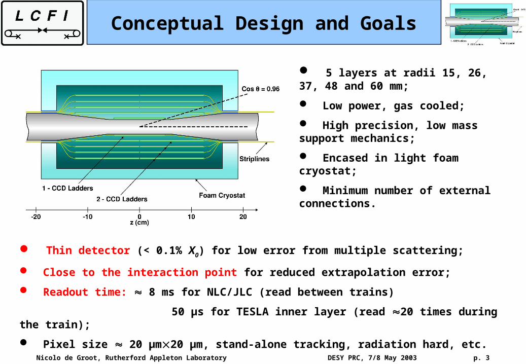
5 layers at radii 15, 26, 37, 48 and 60 mm;
Low power, gas cooled;
High precision, low mass support mechanics;
Encased in light foam cryostat;
Minimum number of external connections.
Conceptual Design and Goals
Thin detector (< 0.1% X0) for low error from multiple scattering;
Close to the interaction point for reduced extrapolation error;
Readout time: 8 ms for NLC/JLC (read between trains)
50 μs for TESLA inner layer (read 20 times during the train);
Pixel size 20 μm20 μm, stand-alone tracking, radiation hard, etc.
Page 4
Nicolo de Groot, Rutherford Appleton Laboratory DESY PRC, 7/8 May 2003 p. 4
Large area, high speed CCDs Inner layer CCDs: 10013 mm2, 2500(V)650(H) pixels per CCD end;
Outer layers: 2 CCDs with size 12522 mm2 , 6250(V)1100(H) pixels;
120 CCDs, 799106 pixels (20 μm square) in total;
For NLC/JLC: readout time 8 ms in principle sufficient, but not easy to achieve with standard CCDs, Column Parallel CCD is desirable;
For TESLA:
50 μs readout time for inner layer CCDs : 50 Mpix/s from each CCD column
Outer layers: 250 μs readout, 25 MHz from each column
Column Parallel CCD is essential
Satisfy TESLA requirements, but thinking about NLC/JLC as well
CPCCD for JLC/NLC could be very advantageous
CCD Development
Page 5
Nicolo de Groot, Rutherford Appleton Laboratory DESY PRC, 7/8 May 2003 p. 5
Electronics only at the ends of the ladders;
Bump-bonded assembly between thinned CPCCD and readout chip;
Readout chip does all the data processing: Amplifier and ADC with Correlated Double Sampling for each CCD column
Gain equalisation between columns
Hit cluster finding
Data sparsification
Memory and I/O interface
CPCCD is driven with high frequency, low voltage clocks;
Low inductance layout for clock delivery.
CCD Ladder End
Page 6
Nicolo de Groot, Rutherford Appleton Laboratory DESY PRC, 7/8 May 2003 p. 6
CPCCDs for TESLA:
Quality of 50 MHz clocks over the entire device (area = 13 cm2):
Power dissipation:
Large capacitive load (normally 2-3 nF/cm2), needs low clock amplitudes;
Low average power ( 10 W) for the whole detector, but large peak power (TESLA duty cycle = 0.5%).
Feedthrough effects:
2-phase drive with sine clocks – natural choice because of symmetry and low harmonics
Ground currents and capacitive feedthrough largely cancel
CPCCDs for NLC/JLC:
Low readout frequency (780 kHz) – in principle few electrons noise could be achieved;
CCD Development
Page 7
Nicolo de Groot, Rutherford Appleton Laboratory DESY PRC, 7/8 May 2003 p. 7
Our First CPCCD (E2V)
Delivered, testing imminent
1-stage source followers and direct connections on 20 μm pitch
Direct connections and 2-stage source followers
Two phase, pixel size 20 μm 20 μm;
Wire/bump bond connections to readout chip and external electronics;
Two charge transport regions;
Serious testing in the following months!
Page 8
Nicolo de Groot, Rutherford Appleton Laboratory DESY PRC, 7/8 May 2003 p. 8
First bump-bondable readout chip (CPR-1)
Designed by the Microelectronics Group at RAL;
Voltage amplifiers for the 1-stage SF outputs, charge amplifiers for the direct connections;
Everything on 20 μm pitch;
0.25 μm CMOS process; scalable and designed to work at 50 MHz;
Smaller chip with ADC arrays and amplifiers already tested;
Work on next generation chip with 22 cluster finding and sparsification has started. Principle demonstrated on 20m pitch.
FIFO
250 5-bit flash ADCs
Charge Amplifiers Voltage Amplifiers
Wire/bump bond pads
Wire/bump bond pads
Readout Chip Design
Page 9
Nicolo de Groot, Rutherford Appleton Laboratory DESY PRC, 7/8 May 2003 p. 9
A program to design CCD support structures with the following properties:
Very low mass (< 0.4% X0 – SLD VXD3)
Shape repeatability to few microns when temperature cycled down to –100 C;
Compatible with bump bonding;
Overall assembly sufficiently robust for safe handling with appropriate jigs;
Thin Ladder R&D
Three options:
Unsupported CCDs – thinned to 50 μm and held under tension
Semi-supported CCDs – thinned to 20 μm and attached to thin (and not rigid) support, held under tension;
Fully-supported CCDs – thinned to 20 μm and bonded to 3D rigid substrate (e.g. Be)
Page 10
Nicolo de Groot, Rutherford Appleton Laboratory DESY PRC, 7/8 May 2003 p. 10
FEA simulations continuing:
Distortions of only few μm, optimise adhesive pitch and size;
Silicone adhesive: NuSil, excellent at low temperature
Layer thickness 0.12% X0
XY stage for 2-dimensional profiling being assembled:
Laser displacement meter
Resolution 1 μm
Models made from steel + unprocessed Si will be measured
CCD brought down
Assembly after shim removal and curing
Beryllium substrate (250 μm)
Beryllium substrate with adhesive balls
Thinned CCD ( 20 μm)
Adhesive
Shims
1 mm
0.2mm
Semi-supported Option
Page 11
Nicolo de Groot, Rutherford Appleton Laboratory DESY PRC, 7/8 May 2003 p. 11
FEA Simulation
Page 12
Nicolo de Groot, Rutherford Appleton Laboratory DESY PRC, 7/8 May 2003 p. 12
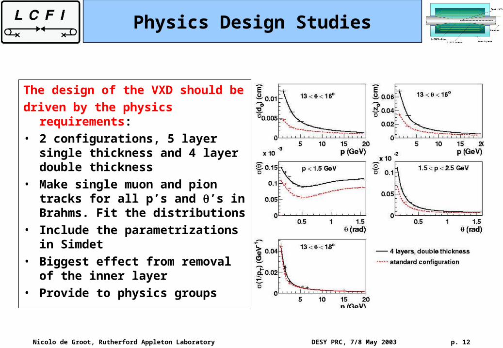
Physics Design Studies
The design of the VXD should be
driven by the physics requirements:• 2 configurations, 5 layer single
thickness and 4 layer double thickness
• Make single muon and pion tracks for all p’s and ’s in Brahms. Fit the distributions
• Include the parametrizations in Simdet
• Biggest effect from removal of the inner layer
• Provide to physics groups
Page 13
Nicolo de Groot, Rutherford Appleton Laboratory DESY PRC, 7/8 May 2003 p. 13
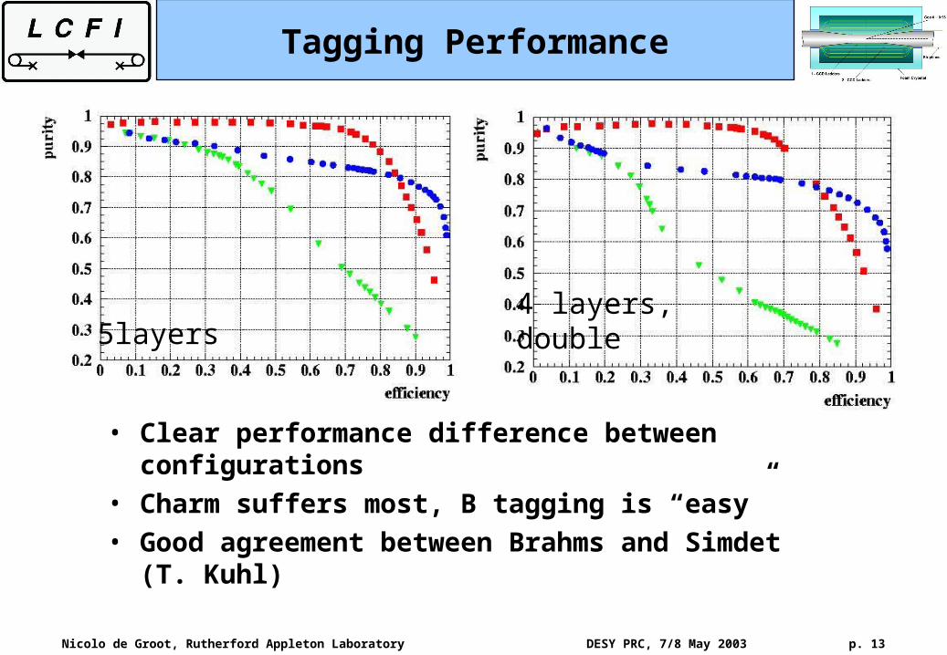
Tagging Performance
• Clear performance difference between configurations
• Charm suffers most, B tagging is “easy”
• Good agreement between Brahms and Simdet (T. Kuhl)
5layers4 layers,double
Page 14
Nicolo de Groot, Rutherford Appleton Laboratory DESY PRC, 7/8 May 2003 p. 14
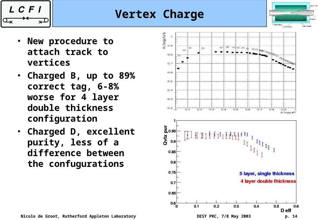
Vertex Charge
• New procedure to attach track to vertices
• Charged B, up to 89% correct tag, 6-8% worse for 4 layer double thickness configuration
• Charged D, excellent purity, less of a difference between the confugurations
Page 15
Nicolo de Groot, Rutherford Appleton Laboratory DESY PRC, 7/8 May 2003 p. 15
Physics Plans
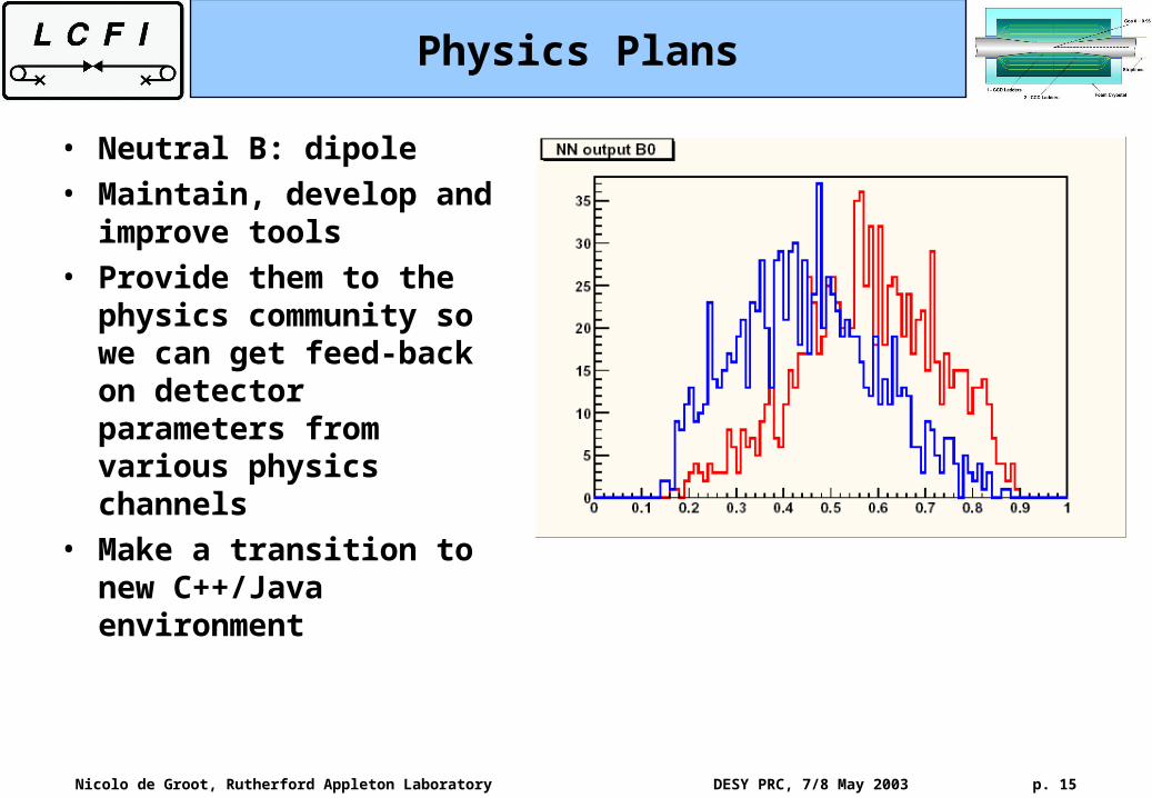
• Neutral B: dipole
• Maintain, develop and improve tools
• Provide them to the physics community so we can get feed-back on detector parameters from various physics channels
• Make a transition to new C++/Java environment
Page 16
Nicolo de Groot, Rutherford Appleton Laboratory DESY PRC, 7/8 May 2003 p. 16
Detector R&D work at the LCFI collaboration:
Development of fast column parallel CCD and its readout chip;
Precision mechanical support of thinned CCDs.
Physics Design Studies
Most aspects of the R&D are applicable to all proposed LC machines;
High speed CPCCDs are mainly for TESLA, however NLC/JLC likely to benefit from slow CPCCDs;
Significant work is required, challenging combination of chip size and speed;
More results to follow in a couple of months.
More information is available from the LCFI’s web page: http://hep.ph.liv.ac.uk/~green/lcfi/home.html
Summary


![Lecture 15-2003p [Compatibility Mode]](https://static.documents.pub/doc/80x56/577dab1f1a28ab223f8bf81e/lecture-15-2003p-compatibility-mode.jpg)


