NIM, CAMAC and VME Standards There have been three major data acquisition standards used in modern nuclear physics. The first to be introduced was the NIM standard and was used to provide power to for the electronics. CAMAC went further and allowed data transfer on the crates backplane. The current standard is VME, expanded on CAMAC by providing more options and a faster bus speed. In today’s modern labs you are likely to find any or all of these standards coexisting. For that reason it is necessary to have a working understanding of all three
Transcript
NIM, CAMAC andVME Standards
There have been three major data acquisition standards used in modern nuclear physics. The first to be introduced was the NIM standard and was used to provide power to for the electronics. CAMAC went further and allowed data transfer on the crates backplane. The current standard is VME, expanded on CAMAC by providing more options and a faster bus speed. In today’s modern labs you are likely to find any or all of these standards coexisting. For that reason it is necessary to have a working understanding of all three
NIM Nuclear Instrument Module
The NIM standard is the first crate standard widely accepted by physicists. It provided a way to organize and distribute power to their electronics. The power was distributed by a series of connectors on the back of the crate. A low voltage power supply is either behind the crate or sat in the crate along side the other modules. Typical voltages distributed were +/-6V, +/-12V, and +/-24V, although many custom power supplies have been built for NIM crates. NIM crateshave 12 slots. Today NIM crates are often used for small setups with only a handful of detectors because their low overhead makes setup easy. They are often used in larger experiments for setup and tohandle logic signals and analog electronics. Some of the most often used modules are amplifiers, gate and delay generators, discriminators, high voltage modules, and linear fan-in fan-out units.
CAMACComputer Automated Measurement and Control
CAMAC answers many of the shortcomings of NIM. CAMAC offers a back-plane that could transfer data. That means the parameters for each channel can be adjusted via the backplane and data can be readout the same way,opening the front panel up for more channels of input. Each CAMAC crate has 25 slots, which meant twice as many modules than a NIM crate. The last two slots in the crate are always reserved for the CAMAC crate controller, which interfaces the crate with a computer. The backplane had one card style connector for each slot, which the modules plugged into.
CAMAC Description
CAMAC is more overhead intensive than NIM because even for small setups programs had to be written and tested. For many years most medium to large-scale nuclear physics were done using CAMAC modules. Typical modules used in a CAMAC crates are ADC’s and TDC’s.
As experiments grew and more modules were needed with a higher channel density the CAMAC bus was not able to keep up. There were several extensions made to the CAMAC modules to help them keep up, FERA bus being the most popular.
Most of the CAMAC crates and modules found in experiments today are there because they were already owned, or the software had already been developed, making the experiment cheaper and/or easier.
CAMAC Card
CAMAC Crate
CAMAC Basics (Node addresses)
CAMAC addresses are node (niche) specific they don’t therefore
have DIL switches that select a particular address, the
programmer must specify a slot when addressing a
module.
����������������������������������
������� ��
����������
�������������
������
�������
CAMAC Basics (Connecting crates)
��������������
������������
��� �����������
���� ���
�����
���� ��
��� ���������
�����������
������
���� ���������������
���� ���
�����
���������������������
���� ���������������
�����������������������
������������������
���� ���
�����
���� ���
����
CAMAC Basics addressing a module
Branch (only single branches at ING always 0 or 6)
Crate (crate addresses range from 0 to 3 at ING the maximum possible is 7)
Node (or Niche!) 25 stations or nodes are available in an a standard CAMAC crate, the rightmost, station 25 is reserved for a crate controller, addressed modules may be plugged into stations 1 – 24
Subaddress used for addressing registers in inside modules, 4 bits are available giving 16 possible subaddresses.
Function used for controlling the available functions within a module, 5 bits are available giving 32 possible functions for diagnostic purposes F 0 read and F 16 write are worth remembering.
CAMAC Basics B C N A F
To communicate with a particular CAMAC module a 4 word address and a 5 bit function code must be specified. The TCS programme reads or writes to most modules at 20Hz. A diagnostic programme is available on the Alpha TCS computer (CAMTEST) for either writingto or examining the contents of module registers
Familiarity with the use of CAMTEST is essential for duty engineers apart from the PLOT program it is the most important tool you have for tackling telescope problems
Remember:- Branch Crate Node Address Function
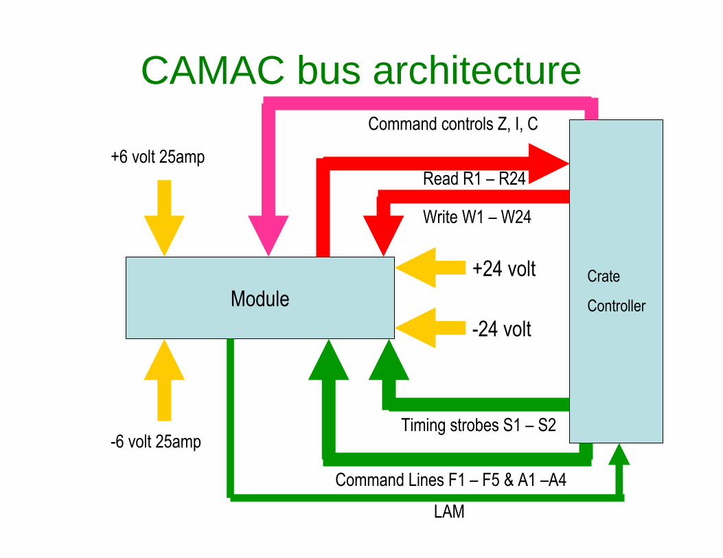
CAMAC bus architecture
���
���������!�����
"���"��# "�$
%����%��# %�$
�����&��������'��# '�
���������������()�*)��
�������+�����,��# ,-�.�/��#/$
+/!
0�$�1��
2�$�1��
0��1����-��
2��1����-��
VMEVersa Module Europa
VME like CAMAC offered a rear backplane for fast and efficient data transfer.
However, VME offered a faster and more versatile bus. The VME bus is industry standard used in physics this means that there is a larger variety of crates and modules commercially available at low prices than for CAMAC.
The faster bus also meant that more data could be transferred and channel density increased. This makes VME a very attractive alternative to CAMAC.
VME SystemVME crate have slots for 21 modules, the first is reserved for a cratecontroller. The VME backplane has two 3-row connectors (J1 & J2) permodule, these are for both data and power distribution. VME also offersoptions for incorporating CAMAC crates into a VME setup this is donewith a VME to CAMAC bridge and allows experimenters to use CAMACmodules and crates they already have keeping experiment cost down.VME is currently the used in most large-scale experiments and is
becoming more popular in smaller scale experiments.VME has several extensions. VME 430 added a third, smaller,
connector to the backplane, called Jaux this connector is used for additional power distribution and user defined operations. VME 64X is an extension of VME 430 and adds two rows of connectors to each of the three connectors, the extra rows were added in such away that a regular VME module would be compatible with VME 64X.
CAEN VMEVME-USB2.0 Bridge
• No boot required, ready at power ON • Up to 30 MByte/s sustained data transfer rate • VME Master (arbiter or requester) • VME Slave (register and test RAM access) • Cycles: RW, RMW, BLT, MBLT, IACK, ADO, ADOH • Addressing: A16, A24, A32, CR/CSR, LCK • Data width: D8, D16, D32, D64 • System Controller capabilities • Interrupt handler • Front panel Dataway Display (available also from PC
and VME)
CAEN VMEVME-PCI Optical Link Bridge
• No boot required, ready at power ON • PC control through A2818/A3818 Optical Controllers • CONET1 OR CONET2 CAEN Proprietary Optical link
Compatible • PCI 32bit / 33MHz (A2818) - PCIe x8 (A3818) • Daisy chain capability • Up to 100 MByte/s sustained data transfer rate (with
CONET2) • VME Master (arbiter or requester) • VME Slave (register and test RAM access) • Cycles: RW, R
CAEN VME• Digitizers• ADCs (Peak Sensing)• QDCs• ADCs C-RAMS (CAEN - Readout for Analog Multiplexed Signals)• Amplifiers (Fast)• Attenuators• Sequencer• HS Caenet Controllers• Controller (VME)• Discriminators• Fan In - Fan Out Units• Coincidence/Logic/Trigger Units• I/O Registers• Scalers• TDCs• Timing Units• Translators• VME High Voltage Power Supplies
CAEN VMEAddressing
CAEN VMESoftware
CAENVMELib LibraryInterface library for CAEN VME Bridges
Set of functions for the control and the use of CAEN VME Bridges
Available for C/C++ enviroment (Windows, Linux) and LabView enviroment (Windows)
if (CAENVME_WriteCycle(vme_handle,V1290_BASE_ADDRESS+CVT_V1190_MICRO_ADD,&wo,cvA32_U_DATA,cvD16)!= cvSuccess) MessageBox(_T("Eroare la scrierea Micro Register"));
if (CAENVME_ReadCycle(vme_handle,V1290_BASE_ADDRESS+CVT_V1190_MICRO_HND_ADD,&data,cvA32_U_DATA,cvD16) != cvSuccess) MessageBox (_T(" V1290 Eroare la citirea Micro Hanshake Register"));
CAEN VMESoftware
if(CAENVME_BLTReadCycle( vme_handle,V1290_BASE_ADDRESS+CVT_V1190_OUT_BUFFER_ADD,&block_buffer[0],in_contor,cvA32_U_BLT,cvD32,&out_contor) != cvSuccess) AfxMessageBox(_T("V1290 Eroare la citirea block"));
Positron Life Time SpectroscopyNIM system
Coincidence Doppler Broadening SpectroscopyVME system
Positron Annihilation SpectroscopyDetectors
CAEN VMESoftware
• Multi Branch System• Standard Data Acquisition System at
GSI• Based on Real-time OS LynxOS (v2.5,
v3.0)• Written entirely in C• CAMAC, Fastbus, VME, VXI GSI trigger
.• M68k CPUs (CVC, Eltec).
CAEN VMESoftware
T9-PS Experimental setup
FPGA - Field Programmable Gate Array
• An integrated circuit designed to be configured by a customer or a designer after manufacturing—hence "field-programmable". The FPGA configuration is generally specified using a hardware description language (HDL), similar to that used for an application-specific integrated circuit (ASIC)
FPGA - Field Programmable Gate Array
Contemporary FPGAs have large resources of logic gates and RAM blocks to implement complex digital computations. As FPGA designs employ very fast IOs and bidirectional data buses it becomes a challenge to verify correct timing of valid data within setup time and hold time.
Xilinx FPGAs - 35
FPGA Evolution of implementation technologies
• Logic gates (1950s-60s)• Regular structures for two-level logic (1960s-70s)
– muxes and decoders, PLAs• Programmable sum-of-products arrays (1970s-80s)
– wires to connect inputs andoutputs to logic blocks
• I/O blocks
– special blocks at peripheryfor external connections
• Add wires to make connections
– done when chip is fabbed
• “mask-programmable”
– construct any circuit
Xilinx FPGAs - 37
Field-Programmable Gate Arrays
• Logic blocks
– to implement combinationaland sequential logic
• Interconnect
– wires to connect inputs and
outputs to logic blocks
• I/O blocks
– special logic blocks at periphery
of device for external connections
Digital FPGA Solutions
Advantages•� Reduction in size (compact)•� Higher resolution•� Lower deadtime•� Multifunctional•� Upgradable•� Possible automation of entire acquisition process•� Remote acquisitionDisadvantages•� Signal requires prefiltering due to ADC limitations•� Complex design procedure (requires knowledge of•C/C++, VHDL/Verilog, Matlab)•� Expensive hardware and software
Digital FPGA Solutions
Unlike microprocessors, FPGAs have to ability to run processes in parallel achieving greater performanceStrict timing constraints allows precise data flow control and time stampingFast reprogramming allows for multi parameter measurements with single setupWide range of experiment parameters can bechanged in real time
“Analog” FPGA Solutions• FPGA devices are considered belonging to digital world
while ADC is an analog measurement function.• ADC can be implemented directly with FPGA plus a few
passive (resistors and capacitors) components.• Bench tests are done for ADC [email protected] MHz and 9-
bit@2MHz. Other speed/resolution combinations are possible.
• The ADC is based on ramp & compare with TDC implemented inside FPGA with 0.69 ns LSB (200ps RMS).
• More than 32 channels of TDC are tested in Altera Cyclone (EP1C6Q240C6, $20) devices.
ADC Using FPGAAMP &Shaper
AMP &Shaper
AMP &Shaper
AMP &Shaper
AMP &Shaper
AMP &Shaper
AMP &Shaper
AMP &Shaper
ADC
ADC
ADC
ADC
FPGA
TDC
TDC
TDC
TDC
R1 R1
C
R2
FPGA
VREF
• Analog signals from AMP & Shapers are directly fed to FPGA pins.
• FPGA output and passive RC network are used to generate ramping reference voltage VREF.
• The input voltages and VREF are compared using FPGA differential input receiers.
• The times of transitions representing input voltage values are digitized by TDC blocks in FPGA.
• Logic elements with critical timing are assigned as shown.
4Ch
Logic elements with non-critical timing are freely placed by the fitter of the compiler.
Digital FPGA SolutionsSpartan 6 SP 605
Digital FPGA SolutionsVirtex 6 ML605
Free running mode FPGA based Data Acquisition
FPGA Programming
VHDL (VHSIC Hardware Description Language) is a hardware description language used in electronic design automation to describe digital and mixed-signal systems such as field-programmable gate arrays and integrated circuits. VHDL can also be used as a general purpose parallel programming language.
FPGA Programming
• VHDL is commonly used to write text models that describe a logic circuit. Such a model is processed by a synthesis program, only if it is part of the logic design. A simulation program is used to test the logic design using simulation models to represent the logic circuits that interface to the design. This collection of simulation models is commonly called a testbench.
• VHDL has file input and output capabilities, and can be used as a general-purpose language for text processing, but files are more commonly used by a simulation testbench for stimulus or verification data. There are some VHDL compilers which build executable binaries. In this case, it might be possible touse VHDL to write a testbench to verify the functionality of the design using files on the host computer to define stimuli, to interact with the user, and to compare results with those expected.
Suggested Reading• Glenn F. Knoll, Radiation Detection and
Measurement, John Wiley & Sons.• Hernam Cember, Introduction to Health
Physics, McGraw Hill.• Nicholas Tsoulfanidis, Measurement and
Detection of Radiation, Taylor & Francis.• C.H. Wang, D.L.Willis, W.D. Loveland,
Radiotracer Methodology in the Biological, Environmental and Physical Sciences, Prentice-Hall
Întreb�ri
• Denumiti standardele de achizitie existente.
• Care este diferenta la adresarea modulelor CAMAC si VME ?
• Ce înseamn� FPGA ?• Care sunt principalele 3 componente ale