N.I.P. SILICON JUNCTIONS DETECTORS Lydie KOCH, Jean NESSIERt Jean VALIN nentre d'Etudes Nucl6aires de SACLAY - FRANCE Abstract- N.I.P. Silicon junctions have been studied as particle detectors. They consist of a 1.000 Q.cm silicon plate on each side of which respeotively a P and N layer have been diffused in order to have a NIP structure. The incident par- ticles 9 to 40 KeV alpha, are parallel with the junctions planes, and strike the detector in the I region. An energy resolution of 2 , and a good linearity of pulse height Ts particle energy up to 40 ReV have been obtained. In addition, gamma rays have been detected with NIP junctions, and pulse §eight distribution of Co60, Cs137 and Hg 3 have beon stu- tied. The average amount of energy expen- ded by a photoelectric elootron In crea- ting one electron-hole pair in silicon has been measured and is found to be s B m 3,53+0,07 eV for 279 keV electrons B- 3, 55+0,1 eV for 660 keY electrons. I - INTRODUCTION The solid state ionisation chamber has been the topic of a great deal of re- searoh during the last few years I to 7. In this device, the region sensitive to radiation is a space charge region in a I J.W. MAYER, B.R. GOSSIK, R.S.I., 27, 407, 1956. 2 A.V. AIRAPETYANTS, Z. Telch. Fiu., 27, 1599, 1957. 3 R. BOMAL, L. KOCH, N'GUYEN V.D., C. SCHNEIDER, Col. Inter. Electr. Nucl. PfRIS 1958, A.I..E.A. VIENNE 1959. 4 Mc. KENZIE, Phys. Rev. Let. 2, 7, 1959. 5 F.J. WALTER, J.W.T. DABBS, L.D.ROBERTS, M.W.WRIGHT, O.R.N.L.58, 11, 9, 1958. 6 S.S. FRIEDLAND, S.N.MAYER, J.S.WIGGINS, Nucl. 18, 2, 54, 1960. 7 G. ANSEL, P. BARUCH, 0. SMULKOVSKI; C.R. Acad. Scie. 250, 1468, 1960 Nuel. Inst. and Methods. Germanium or Silicon crystal. Because the incident particles penetrate into the crystal perpendicularly to the Jun- ction plane, the range of linearity of response vs particle energy is dependant upon the width of the depletion region which is limited by the resistivity of the base material (700 microns with 13.000 Q.cm silicon) 2. In the gata presented, another type of detector has been investigated. It consists of a nearly intrinsic silicon plate (1000 Qf.cm P type) on each side of which respectively a P and N layer have been diffused : this gives the so called NIP structure in which the depletion re- gion extends to the whole I region when sufficient reverse bias is applied. Two sets of experiments have been performed: 10) The response of the detector to alpha particles with energies up to 40 MeV has been studied. The incident particles are parallel to the junction plane so that a great penetration range is allowed without loosing energy out- side of the depletion region. 20) Individual gamma rays have been detected and the average energy N expen- ded by an alectron in creating one elec- tron-hole pair has been measured : it is also shown that the energy loss per electron-hole pair is independant of the energy and the nature of the particle, either alpha or beta. II - NIP JUNCTION CHARACTERISTICS Figure 1 illustrates the NIP junction detector. Its dimensions are 8 ; 1 ,1 I 0,28 mm. Two layers, respectively P type and N type, have been diffused on the 8 Made by the "CO14PAGNIE FRANCAISE THOMSON HOUSTON . "3
Transcript
N.I.P. SILICON JUNCTIONS DETECTORS
Lydie KOCH, Jean NESSIERt Jean VALINnentre d'Etudes Nucl6aires de SACLAY - FRANCE
Abstract- N.I.P. Silicon junctions havebeen studied as particle detectors. Theyconsist of a 1.000 Q.cm silicon plate oneach side of which respeotively a P andN layer have been diffused in order tohave a NIP structure. The incident par-ticles 9 to 40 KeV alpha, are parallelwith the junctions planes, and strikethe detector in the I region. An energyresolution of 2 , and a good linearityof pulse height Ts particle energy upto 40 ReV have been obtained. In addition,gamma rays have been detected with NIPjunctions, and pulse §eight distributionof Co60, Cs137 and Hg 3 have beon stu-tied. The average amount of energy expen-ded by a photoelectric elootron In crea-ting one electron-hole pair in siliconhas been measured and is found to be s
B m 3,53+0,07 eV for 279 keV electrons
B - 3, 55+0,1 eV for 660 keY electrons.
I - INTRODUCTION
The solid state ionisation chamberhas been the topic of a great deal of re-searoh during the last few years I to 7.In this device, the region sensitive toradiation is a space charge region in a
I J.W. MAYER, B.R. GOSSIK, R.S.I., 27, 407,1956.
2 A.V. AIRAPETYANTS, Z. Telch. Fiu., 27,1599, 1957.
3 R. BOMAL, L. KOCH, N'GUYEN V.D., C.SCHNEIDER, Col. Inter. Electr. Nucl.PfRIS 1958, A.I..E.A. VIENNE 1959.
7 G. ANSEL, P. BARUCH, 0. SMULKOVSKI;C.R. Acad. Scie. 250, 1468, 1960Nuel. Inst. and Methods.
Germanium or Silicon crystal. Becausethe incident particles penetrate intothe crystal perpendicularly to the Jun-ction plane, the range of linearity ofresponse vs particle energy is dependantupon the width of the depletion regionwhich is limited by the resistivity ofthe base material (700 microns with13.000 Q.cm silicon) 2.
In the gata presented, another typeof detector has been investigated. Itconsists of a nearly intrinsic siliconplate (1000 Qf.cm P type) on each side ofwhich respectively a P and N layer havebeen diffused : this gives the so calledNIP structure in which the depletion re-gion extends to the whole I region whensufficient reverse bias is applied.
Two sets of experiments have beenperformed:
10) The response of the detectorto alpha particles with energies up to40 MeV has been studied. The incidentparticles are parallel to the junctionplane so that a great penetration rangeis allowed without loosing energy out-side of the depletion region.
20) Individual gamma rays have beendetected and the average energy N expen-ded by an alectron in creating one elec-tron-hole pair has been measured : it isalso shown that the energy loss perelectron-hole pair is independant of theenergy and the nature of the particle,either alpha or beta.
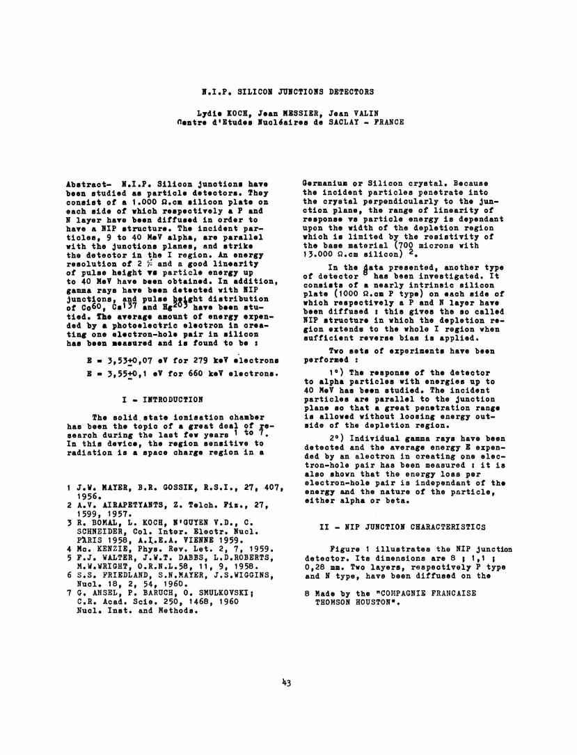
II - NIP JUNCTION CHARACTERISTICS
Figure 1 illustrates the NIP junctiondetector. Its dimensions are 8 ; 1 ,1I0,28 mm. Two layers, respectively P typeand N type, have been diffused on the
8 Made by the "CO14PAGNIE FRANCAISETHOMSON HOUSTON .
"3
sides, to a depth of 80 microns.
Reverse current at 2900 K is shownin table I
Table I
NO of the diode 1 2 3 4
.IiA (v = -1oov) 0,54 :0,16 *0,40 00,21
Il1A (V = -500V) 0,8 0,440,94 :0,6* .
s- . _ s
Capacitance and width of the deple-tion region vs reverse bias are shown inTable II.
Table II
"V::volts.2"PF,t X
tI"eit p
- 5
28,5 :
32,8
it
25 : - 30 :- 160:- 300"
*It
13,5 9,8 8,1 7, ,
* I*
68 94 : 114 : 117
: :it. . . .
If one plot capacitance vs reversebias (Fig. 2 ) the graph shows that theNIP junction capacitance saturates whenthe reverse bias is higher than 70 V.
For bias values lower than 70 V,the width of the depletion region at theNI junction (I for high resistivity Ptype) is given by :
e = 3 (f ve : width of the depletion region
in microns
resistivity in Q.cm
V: reverse bias in volts.
Because of the IP junction impedance,connected in series with the NI junctioncapacitance, the experimental measurementsof the latter are not accurate and theresulting values of the depletion regionwidth are over estimated.
Also, it seems that the resistivityof the base material has strongly in-creased owing to the diffusion process.When reverse bias is 70 V, the depletionregion, between the N and P layers extendsto the P region.
For reverse bias values higher than70 V, the depletion region increasesslightly in the N and P region, and capa-citance is nearly constant.
III a PARTICULE AND
PROTON SPECTROMETRY
All detectors have been employed inair at room temperature. The incidentparticles, parallel to the junction plane,penetrate into the I region which has asengitive area of 8 x 0,12 mm2 ; the depthof the sensitive region is then 1, 1 mm,allowing measurement of higher energiesthan was previously possible. The detec-tors have been irradiated with oa parti-cles of various energies, 8,7 NIeV (Tho-rium CI), 24,8 MeV, 32 M4eV, and 39,6 MeVfrom the SACLAY cyclotron, these energiesbeing known with an accuracy of betterthan 1/500.
The arrangement of electronic equip-ment is shown in Figure 3. The reversebias applied to the crystal is 150 V. Thetotal voltage induced by a 40 MeV alphaparticle is 60 mV and is magnified 1000times with a linear amplifier. The pulseheight distribution is analysed in a 256Channel Analyser, calibration measure-ments being made by injecting pulses intothe crystal through a capacitor C' witha highly stable mercury-relay pulse gene-rator having an output attenuator linearto 0t1 2%.
The bandwidth of the amplifier (C.E.A.Amp. 49) stretches from 100 to 900 kHz ;its noise level is then 6 )iVrms ; the noi-se level of the crystal, biased at 150 V,is 12 liV rms with the same bandwidth. The-refore, crystal and amplifier noise sets alower theoretical limit to resolution.This amounts to 5.10-4 with 40 MeV mono-energetical alpha particles, that is fullwidth of 20 keV at half maximum of thepulse height distribution. In fact, becau-se of the ambiant noise high level inthe cyclotron room, the lower limit ofresolution was found to be 0,7 %- in theactual experiment.
Energy resolution.-
Resolution is at present better than2 % at 40 14eV for alpha particles (Fig.4).
It is to be noticed that the inci-dent particles striking the detector inthe P or N region far from the sensitiveregion induce lower pulses than those pro-.duced when the incident particles pene-
: : 0 s
trate into the depletion region, becauseof the volume recombination outside ofthe space charge region. This effect contzi-butes to widen the pulse height distribu-tion peak towards the lower energies, thuslimiting the effective energy resolution.
Therefore, it should be expected thatone could obtain a better energy resolu-tion when using a NIP structure with thin-ner N and P layers ; these layers can bereduced to the tenth of their present widthwithout any important change in the currentvoltage characteristicsof the diode.
Linearity of pulse height vs particleenergy.-
Fig. 5 shows that the variation ofpulse height with.alpha particle energyis linear to within 1 574, once the energyloss by the alpha particles impassingthrough 5 cm of air before striking thedetector has been taken into account. Thecapacitor C' has been measured with anaccuracy of better than 1 % ; therefore,taking the energy loss per electron-holepair E = 3,5±0,05 eV, according to thepublished values, it is possible to calcu-late the charge collection efficiency: ithas been found to be 100 %.
IV - INDIVIDUAL DETECTION OF GAMIMA RAYS
The spectrometry of beta particleswith NP Silicon junctions has been demons-trated 9 but no data on gamma ray specstro-metry has yet been published. In thislaboratory individual gamma rays fromHg2O3, Csl 7 and Co60 have been detectedwith an N-IP Silicon junction counter. Thecrystal area was reduced to 1 mm2, theNIP -structure remaining the same as before.The device, sealed in an evacuated glassbulb, is operated at room temperature.
A Compton or a photoelectron resul-ting from the absorbtion of the incidentgamma rays produces electron-hole pairsin the crystal, and the total amount ofcharge produced in the depletion region,collected across the barrier, is measured.Then the collected amount of charge dependsupon the ratio: range of the beta parti-cle/dimension of the collection region.Also, the Compton electrons have variousenergies ) therefore, the pulse heightdistribution extends from 0 to a maximumamplitude, Am. With gamma rays from Hg2035and Cs137, the maximum amplitude, Amt hasbeen measured and corresponds to the in-cident gamma ray energy. In the case of
9 Mac KENZIE, J.B.S. WAUGH, VII Scintil-lation Counter Symposium Washington 1960.
Hg2O3, the pulse height spectra shows aphotoelectric peak (Fig.6) ; the energyresolution is 8 % and when the source isremoved, no pulse greater than 70 keVappears during a time of 15 hours.
From the maximum pulse height corres-ponding to photoelectrons it is possibleto calculate the average energy loss byan electron in creating one electron-holepair. It has been found that the valueof E is :
3,53±0,07 eV for 279 keV beta particle
3,55±t0,1 eV for 660 keV beta particle.
Within the accuracy of measurements,it is the same value as those publishedrecently for alpha particles or protons,namely E = 3,50±O,05 eV.
This is due to the fact that most ofthe electron-hole pairs resulting fromthe passage of an alpha particle throughthe crystal are produced in fact by deltarays which are beta particles with energyof a few keV. This agrees very well withSHOCKLEY's data presented at the PRAGUEConference 10 to a first approximation,the average energy for electron-hole pairdepends only upon the forbidden energy gapof the material and upon energy emittedas phonons.
It should be noticed that a value ofE for 25 M1eV beta particles has alreadybeen published
E = 4-,8 0,7 eV
V - FURTHER REMARKS
10) High energy alpha particlesandprotonsspectrometry .-
With a PN junction, the maximum ener-gy that can be measured is limited by thewidth of the depletion region (about 500microns at the present time). Since inan NIP structure, the only condition formeasuring the energy of a particle isthat it loses all its energy in the slicebetween two heavily doped regions, then,under present day conditions it wouldseem possible to manufacture an NIP detec-tor with dimensions 1, 10, 15 mm so thatone could measure an energy as great as100 MeV for an alpha particle with a
10 W. SHOCKLEY, IV Conf. Intern. sur la.Physique des Semi-conducteurs PRAGUE1960 (h paraitre)
11 V.A.J. VAN LINT, H.ROTH, E.G.WIKNER,Bull. of the Am. Phys. Soc. II, 4, 8,457, 1959.
25
solid angle of 2,5.10-2 steradian.
20) Measurement of the specificionization of high energy particles.-
With a thinner device (200 micronsfor instance), one can measure the amountof energy lost through the crystal byhigh energy particles incident perpendicu-larly to the junction plane, so as to havethe value of the specific ionization dE/dx;thus a minimum ionizing proton loses about100 keV through 200 microns of Silicon. Atpresent, this energy can be measured withan accuracy of better than 10 % with theNIP device.
CONCLUSIONS
With the aid of semiconductor NIPstructures it is possible to increase therange of particlea spectrometry towards
higher energies t the present limit being40 MeV alphas with an NIP detector. Inaddition, owing to the weak reverse currentof the NIP junction, minimum ionizing par-ticles (beta, protons), loosing not muchmore than a few tens of keV in the sensi-tive region can be detected ; furthermorethe sensitive volume of such a detector islarge enough to measure the energy of gam-ma rays.
ACKNOWLEDGMENTS
Thanks are due to Mtl. MAILLARD andBOBENRINCK of the Compagnie Fran9aiseThomson-Houston for manufacturing thecrystals and to MM. SODINOS and CHAIIINADEfor their cooperation in the experimentsperformed with the Cyclotron.
DIODE NIP (CFT )
Cor a Lteristiqve Csro t -Tansion :
Inverse V: 150 VOLS
V :250 VOILs
DirttL : Vs200 Volts
I: 0,2 VAi. 0.4 pA
I. tA
C 10 p F pour Vi . 100Volts
Fig. 1. Geometrical and electrical characteristics of the N.I.P. Silicon
416
DIODE NIP CFTH
VARIATION DE LA CAPACITE EN FONCTION
Tesslin inverse oppliques
Fig. 2. Capacitance versus reverse bias for N.I.P. counter.
SCHEMA DU MONTAGE ELECTRIQUE
Gt iafr tour
d impuluemos ft. learnin
22ML
Fig. 3. Schematic diagram of electronics shoving connections to 15e preamplifierand test pulser. The capacitor Cc was approximately 10- Farad.
47
a
10
.2
.2
.0~-
DIODE NIP IRRADIEE PAR LA TRANCHE
Vi * 170 Volts
od 38.6MeV R . 2%
'OUVOIR DE RESOLUTION
04 38.6 MeV
( Cyclotron )
| 790 KcV
Imp lsionsd&tolonnqge~~~~ l _ ~~~~~~~~~~~R I0.O,7,0
10 150 160 170 180 190 2 210N° Conol
Fig. 4. Pulse height spectrum of Cyclotron o rays N.I.P. counter 150 volts bias.
DIODE NIP IRRADIEE PAR LA TRANCHE
* 20V LINEARITE EN FONCTION DE L ENERGIE
38,6 MeV
30,8 MeV
io-0 23,3MeV.2
In/
L ,78MeVE£ (Thorkum C')
10 20 30 40En e d yoyns a en MeV
Fig. 5. Response of N.I.P. counter to a rays penetrating the crystalparallely to the junction plane.