47
AD-A133 780 A PROGRAMMABLE V0ICE PROCESSOR FOR OIHTER AIRCRAFT J/ LINCOLN LAB E M HOFSTETTER ET AL. 18 AUG 83 TR-653 UNCLASSIFIED ESD-TR-83-037 F19628-80-C-0002 F/G 17/2 NL NO "1W
| Date post: | 16-Mar-2018 |
| Category: |
Documents |
| Upload: | truongdung |
| View: | 212 times |
| Download: | 0 times |

AD-A133 780 A PROGRAMMABLE V0ICE PROCESSOR FOR OIHTER AIRCRAFT J/LINCOLN LAB E M HOFSTETTER ET AL. 18 AUG 83 TR-653
UNCLASSIFIED ESD-TR-83-037 F19628-80-C-0002 F/G 17/2 NL
NO "1W

L6 1.8
liii .1 ~ II1)8111111.
-15 11111_L 16
MICROCOP'Y RESOLUTION TEST CHART

Technical Report 653
E.M. HofstetterE. Singer
A Programmable Voice Processor J. Tierney
for
Fighter Aircraft Applications
18 August 1983
Prepared fom dhe Department of the Air Forceunder Electonic Systems Divson Contract F1g629-80M..- by
Lincoln LaboratoryMASSACHUSETTS INSTITUTE OF TECHNOLOGY
LUxiG7oN, MASSACHUSETT
S LET
83 10 19 n

The week rtud Im thib document was iudems at Linam Labmeasoy, a sefor usmrrs epomeed by Maohuueus Iutku of Tochamoy. with the sopps ofshe Depmeemem al th Air Forme nder Oaowc FlSJS.C4 L
This vepece may be npnodued to matisfy ne.of U.S Govremmmeng andes.
m ndcmdudoscomealnedthsdocument to.1e conuatoshould not be inteapeetedf as ammeily represeaning the officlil poliie, eitherexpeemed or implied, of the United State Goveamet.
Mwe Public Affalr Office hs reviewed this repaint, and it isreleasble to the National Technica l nfoution Service,where it wI be avalable ao the generl public, indudingWoeign nationailo.
Thi technica rpan hIs been reviewed aind is appoved for publication.
FOR THE COMMANDER
Thomas J. Alpeet Majort, USAFCid, ZSD Lincoln Laboaw"e Prowec Office
No-um %*is

MASSACHUSETTS INSTITUTE OF TECHNOLOGY
LINCOLN LABORATORY
A PROGRAMMABLE VOICE PROCESSOR
FOR
FIGHTER AIRCRAFT APPLICATIONS
F.M. HOFSTETTER
E. SINGER
J. TIERNEY
Group 24
TECHNICAL REPORT 653
18 AUGUST 1983
Approved for public release; distribution unlimited.
LEXINGTON MASSACHUSETTS

ABSTRACT
'A flexible, high-speed digital voice processor has been designed for use
in conjunction with the JTIDS communication terminal to be installed for
testing on board F-15 fighter aircraft and in Army JTIDS installations. The
processor, known as the Advanced Linear Predictive Microprocessor (ALPCM),
has an architecture which is similar to that of its predecessor [1] but
contains significant improvements in speed, memory, and software development
aids. The design includes an arithmetic section (four AMD 2901C bit-slice
RALUs and an AMD 29517 16x16 multiplier), a doubly pipelined control path,
and an I/O section based on a finite state machine implementation. Microcode
development is enhanced by the presence of an interactive debugging system
consisting of a plug-in monitor board controlled from a host computer. The
ALPCM is capable of implementing conventional 2400-bps LPC vocoders in real
time and is sufficiently powerful to accommodate more sophisticated,
computationally intensive algorithms should the extra performance they
provide be required in the severe F-15 operational environment.
Accession For
NTIS GRA&IDTIC TABUnannouncedJustificatioL-
ByDistribution/
Availability CodesAvail and/or
Dist Special
rioe

TABLE OF CONTENTS
ABSTRACT
I. INTRODUCTION 1
II. THE ALPCM SYSTEM 2
A. Architecture 2
B. Instruction Format 10
C. Data Memory Addressing 14
D. Firmware Considerations 15
E. Engineering Considerations 15
III. DEVELOPMENT SYSTEM 16
A. Monitor 16
B. Assembler 23
C. Simulator 23
IV. SUMMARY AND CONCLUSIONS 25
ACKNOWLEDGEMENT 27
REFERENCES 28
APPENDICES
Appendix A - The ALPCM Assembly Language 29
Appendix B - Monitor Command Descriptions 34
Appendix C - Simulator Command Descriptions 36
Appendix D - Interrupt Logic Equations 38
Appendix E - ALPCM Specifications 39
tv

I. INTRODUCTION
Lincoln Laboratory has been actively engaged in developing techniques
for improving the performance of narrowband voice digitizers for use in
airborne and ground-based military operating environments. Specifically,
Lincoln has been asked by the USAF JTIDS Joint Program Office to develop a
2400-bps voice capability for the JTIDS class 2 terminal (fighter aircraft
and selected ground installations) with an emphasis on compatibility with the
DoD narrowband standard for 2400 bps. During the past two years, Lincoln has
measured the acoustic ambient and electrical noise associated with aircraft
and surface installations which will use JTIDS equipment (e.g., F-15, E-3A),
studied the speech distortions introduced by oxygen face masks and gradient
microphones, and studied the effects these noises and distortions have upon
the intelligibility and quality of narrowband digitized speech.
In order to validate the use of various 2400 bps vocoding techniques in
actual operational environments, it has been necessary to design a small,
low-power, fast digital signal processor capable of functioning in an
environmentally hostile F-15 test aircraft. This signal processor, called
the Advanced Linear Predictive Microprocessor (ALPCM), has sufficient speed,
memory and flexibility to support real time emulation of a number of
candidate 2400-bps vocoders. With such a flexible, programmable processor,
it will be possible to test the acceptability of several 2400-bps coding
algorithms in live aircraft or ground environments populated by military
users.
The basic architecture of the ALPCM is that of a general purpose
computer with a single input bus and separate output bus. Besides a 16-bit
I
..... . ..... ... . .. . i ' " '/ .. ." . .. . .

arithmetic unit comprised of four, 4-bit slice Register-Arithmetic Logic
Units (RALUs), the computer has a stand-alone 16x16 multiplier and separate
program and data memories to allow overlapped pipelined operation in a single
machine cycle (Harvard architecture). The ALPCM's use of a bit slice
implementation approach was made necessary by the need for both speed and
flexibility of operation. Although various single chip microcomputers and
signal processing chip sets are now commercially available, none of them
allows the realization of a processor structure that is both fast enough
(cycle time 100-150 ns) and flexible enough to implement a wide class of
speech coding algorithms at 2400 bps. In the case of general purpose single
chip microcomputers, the cycle time is much longer than 150 ns. In the case
of fast signal processing chips, the limited on-chip memory implies the need
for a multiple processor structure containing several such chips. This
limits the ability to implement a large class of vocoder algorithms without
special purpose techniques.
The ALPCM is the second generation of a similar processor [1] that was
designed and built in 1976 to implement an autocorrelation type LPC
vocoder [2]. The present computer is smaller, requires less power, has twice
the data and program memory and runs with a faster cycle time than the
earlier machine. All of these properties make it suitable for use as a
flyable algorithm evaluation tool for fighter and surface environments.
II. THE ALPCM SYSTEM
A. Architecture
The basic block diagram for the ALPCM is shown in Fig. 1. All
instructions for this machine including the multiply are executed in 100 ns.
2

rwU
z _ c0
0(
cx~ L-
09,
cco
C.) Ix
LM1
D (D x
o 0
co C
3xC

The computational section of the system is based on a 16-bit CPE fabricated
from four AMD 2901C 4-bit RALUs coupled with a carry-lookahead chip. The
2901C is architecturally identical to its predecessor, the 2901, but is much
faster because it uses ECL technology internally. A simplified block diagram
of the 2901C is shown in Fig. 2. From this diagram, it is seen that the
2901C consists of an ALU capable of addition, subtraction and Boolean
operations coupled with an internal, 16-word, two-port register file.
Multiplexers at the input of this file permit a one-bit up- or down-shift
prior to writing into the file. An additional register, the Q-register, is
supplied to facilitate double precision shifts. The ALU inputs can be chosen
from the register file, the Q-register or the outside world via the D input
pins. The operation performed by the 2901C is determined by the state of the
inputs to its various control pins. These inputs, as well as all other
control lines in the ALPCM, are controlled directly by bits in the
instruction register to be described in detail later. The manufacturer's
data sheet should be consulted for further details.
Reference to Fig. 1 shows that the CPE is connected to an input and an
output data bus. The input bus is connected in a tri-state fashion to 7
sources: the 16-bit data memory output register (MOR), the 12-bit
analog-to-digital converter (ADC), the 8-bit serial-to-parallel converter
(SPC), the 12-bit memory address register (MAR), the 16-bit upper and lower
products coming from the multiplier chip (UP, LP), and a 12-bit immediate
field (IF) coming from the instruction register. A 3-bit field in the
instruction register controls which device is activated onto the input bus.
The data memory consists of 2048 words of RAM plus 2048 words of PROM used to
4
aw>

113°0509 Sl
1-BIT SHIFTER SELECT
A. B ADDRESS 2-ADDRESSI-TSHF
MEMORY,,-I.O s-(control) r FILE (16E
G-REGISTER
LATCH LATCHFROM
E
MEMORY, TO EO,0
COTO IR - A
0--DFUNCTION ARITHMETIC LOGIC UNITDECODE
TO MEMORY, 1/0
Figure 2. 2901C RALU block diagram.

store the various tables needed for the speech dig, ization algorithms.
The output of the CPE is routed to 6 devices: the 16-bit memory buffer
register (MBR), the 12-bit MAR, the 12-bit digital-to-analog converter (DAC),
the 8-bit parallel-to-serial converter (PSC), and the 16-bit multiplier and
multiplicand inputs (X,Y) to the multiplier chip. The various output devices
are clocked under control of a 3-bit field in the instruction register.
The multiplier chip is an AMD 29517 which can perform a 16x16 multiply
yielding a 32-bit product in less than 80 ns (military specifications). Both
inputs and outputs are fully buffered on chip thus eliminating the need for
any additional hardware. The chip will perform either fractional or integer
multiplies under the control of a single format adjust pin which is connected
to a dedicated bit in the instruction register.
Referring once again to Fig. 1, it is seen that the instruction register
is 48 bits wide and is driven by a 4096 word program PROM. The address is
obtained from the next-address logic which determines the next address using
information coming from the instruction register, the CPE status bits and the
interrupt request lines. The central component of the next address logic is
an AMD 2910 program sequencer chip for which a simplified block diagram
appears in Fig. 3. This diagram shows that the 2910 generates a 12-bit
program address which can be selected from among the following choices: the
last program address plus one, an absolute branch address obtained from the
12-bit instruction field, a 12-bit address popped from an internal LIFO
stack, or an internal register. The last option is not used in the ALPCM.
The choice between the incremented program counter and the branch address
depends on whether a branch instruction is presently in the instruction
6

BRANCH/COUNTERINPUT
112
REGISTER/!COUNTER
OUT 5 x 12
STACK
4 :1 M UXIN R M T
X 12
OUTPUTADDRESS
Figure 3. 2910 sequencer block diagram.
7
k*1

register and whether the branch condition is met. Any branch instruction
also can be a subroutine call by causing a return address to be pushed onto
the 2910's internal stack. Subroutines may be nested four deep when
interrupts are active and five deep otherwise. The next address is popped
off the stack only when the subroutine return bit is set in the instruction
register.
Note that the address generated by the next-address logic is first
buffered in the P register before being used to address the program memory.
This additional level of pipelining in the control path was needed to make
the speed of the control path commensurate with that of the arithmetic path.
The I/O system for the ALPCM consists of two input channels, the ADC and
SPC and two output channels, the DAC and PSC. The ADC and DAC run on a
common clock that is derived from the system clock. The PSC and SPC run on
external modem generated clocks which must have the same nominal frequency
but are otherwise asynchronous. The ADC/DAC clock period is derived from the
system clock using an AMD 9513 System Timing Controller. This is a
programmable chip which, among other things, will allow the ADC/DAC clock
period to be set under program control.
Each of the I/O channels generates an interrupt request whenever its
associated clock presents a rising edge to the system. A simplified block
diagram of the interrupt logic is shown in Fig. 4. The input edge detectors
convert the rising edge of the I/O associated clock into a pulse whose
duration is equal to the system clock period, 100 ns. The remainder of the
interrupt logic is realized as a finite state machine using a single MMI
PAL16R8 programmable array logic (PAL) chip. The 4-bit state memory serves
to remember pending interrupt requests that result when a request arrives at
8

U0 LU
LUU
Lu 00 $--
a U, * -0
c U Ca
_ 00
0 V)
I .- C-ccZ C
z(J 4
CC t9

a time when interrupts are locked out by an instruction register bit
controlled by the software. These state bits are cleared, one by one, and
interrupt acknowledges (int, dint) are produced as the corresponding
interrupts are granted when the interrupt enable bit is again set by the
software. Along with each interrupt acknowledge, a 2-bit interrupt vector
(vi, vo) is produced. This vector and the acknowledges int and dint are used
to override the 2910 sequencer and force the machine to execute the two
instructions located at addresses 111111111v 1v00 and 111111111vlv 01. The
interrupt sequence also causes the proper return address to be pushed on the
2910's stack so that a return from the interrupt service routine can be
effected by issuing a subroutine return instruction. The detailed logic
equations governing the finite state machine are given in Appendix D.
The mechanism whereby the return address is pushed onto the 2910's stack
when an interrupt occurs is not foolproof. Situations can arise when an
incorrect return address will be saved. It is the responsibility of the
programmer to avoid these situations by locking out interrupts during certain
code sequences. The rule for accomplishing this is to lock out interrupts on
every instruction where either of the following two instructions to be
executed contains a jump. It is also the responsibility of the programmer to
lock out interrupts during an interrupt service routine if this effect is
desired. Interrupts may be nested as long as the 5-word stack capacity is
not exceeded. Other situations requiring care on the part of the programmer
are discussed in the next section.
B. Instruction Format
The format of the 48-bit wide instruction word is shown in Fig. 5. This
word is divided into fields of various length whose functions now will be
detailed.
10
.. .... .. . ~ - ' ... -. .

1 3 3 3 3 3CO 01 I Id IC4 1 1 4 3 111
JPC R
1 1 1 1 12
C IC L I
Figure 5. Instruction format.
11

The Co, Is and 10 fields go directly to the CPE and determine the
exact operation it is to perform, e.g., add the contents of the internal
register at address A to the contents of the internal register at address B,
or take the contents of the internal register at address A and logically AND
it with the external data present on the D-pins. A detailed list of useful
combinations of these fields and the other fields to be described in this
section along with a mnemonic for each is given in Appendix A.
The Id field also goes directly to the CPE and determines where its
ALU output is to go. Some examples are: the output of the CPE alone, the
output of the CPE and the internal register file at address B or the output
of the CPE and the internal register file at address B, but first shifted up
or down by one bit.
The IC and OC fields determine from where the CPE gets its D input and
where its output is to be stored, respectively. The decoded IC field
controls the tri-state enable pins of the various devices connected to the
input bus and the OC field controls logic that generates clocks for the
registers connected on the output bus. The A and B fields go directly to the
CPE where they determine the addresses for the 2-port internal register
file. The single FA bit goes to the multiplier where it is used to select
fractional or integer format for its output.
The JPC field, along with the S and R fields, go to logic that enables
the 2910 program sequencer to implement conditional program branches,
subroutine calls and subroutine or interrupt returns. A detailed list of the
possibilities appears in Appendix A. Conditional jumps in the ALPCM are
12
...........................

somewhat unconventional in that the condition to be sensed by the juip
instruction must be established by the programmer by means of the '1'T field
in an instruction prior to the instruction containing the jump. For example,
if one wishes to jump conditionally depending on whether one of the CPE's
internal registers is zero or not, the contents of this register must be made
to appear at the CPE output during an instruction that also has the TST field
active (LOW). This strobes the 3-bit CPE status into the status register
which then may be tested by a subsequent instruction containing the
appropriate conditional jump code. The three status bits are: F=O (ALU
output zero), the sign bit at the CPU output, and the most significant carry
out. Only the first two status bits are used as jump conditions. ALPCM
jumps also have the unusual property that the instruction following the jump
instruction is executed before the actual jump to the new address takes
place. This behavior is a consequence of the fact that the control path is
doubly pipelined due to the presence of both a P register and an instruction
register. Clever programming can be used to exploit this fact or else a
"noop" can be inserted after the jump instruction.
The status register is not saved during interrupts. If an interrupt
service routine alters the status register, then the background program must
lock out interrupts at appropriate times. Interrupts must be locked out on
the instruction doing the test, on the two preceding instructions and kept
locked out until the result of the test is sensed by a conditional jump. The
necessity for this odd protocol is the fact that when an interrupt request is
granted, the following two instructions will be performed before the
interrupt service routine is entered.
13

The immediate field IF consists of 12 bits that are connected in a
tri-state fashion to the input bus where they can be used as data. They also
are connected separately to the direct input of the 2910 where they are used
as the branch address during successful jumps.
The remaining fields are all 1 bit long. The machine will halt when it
encounters an instruction with the HLT bit set. This feature is useful when
writing diagnostic programs. When the ECY bit is set, the carry in to the
CPE uses the output of the carry-save flip-flop instead of CO from the
instruction word. This feature is used to implement multiple precision adds
and subtracts. An instruction with the IE bit set can be interrupted as
discussed above. Finally the TCE bit is used to enable the 9513 System
Timing Controller chip. When LOW, the 9513 will interpret the A address
field as one of its instructions. This mode usually is used only when the
machine is being initialized. One bit of the instruction register is unused.
The state of the multiplier is not saved automatically during
interrupts. If necessary, this must be done by the programmer by locking out
interrupts from the time the multiplier and multiplicand are loaded until the
product is read. The technique described above for locking out interrupts
during a test/conditional-jump sequence also is required here.
C. Data Memory Addressing
Addresses of the ALPCM data must be generated in the CPE and then
deposited in the MAR. Direct addressing of data memory is achieved by having
the desired address in the IF field of the microinstruction word and passing
It through the CPE to the MAR. Indexed addressing can be accomplished by
having a base address In the immediate field, adding to it the contents of a
14
...... .... . - ' V . .. ., _ _ _ _

CPE internal register, and depositing the result in the MAR. It should be
noted that the contents of the addressed location in data memory are
available only as a CPE input one instruction cycle after the desired address
is placed in the MAR. This is due to the fact that the memory output is
buffered in the MOR. Writing data memory is also a two-step process in the
sense that the address first must be calculated and deposited in MAR before
the datum itself may be read out into the MBR. The hardware has been so
configured that the contents of the MAR can be used as an input to the CPE.
This was done so that the contents of the MAR could be saved when entering an
interrupt service routine and restored when exiting.
D. Firmware Considerations
Two 2400-bps vocoder algorithms have been implemented on the ALPCM, the
Lincoln LPC-10 algorithm [2] and a DoD standard LPC-10 compatible algorithm
[6]. The Lincoln algorithm uses approximately 1000 data memory locations
(60% ROM and 40% RAM), 1000 program locations, and requires 45% of real time
for execution. The corresponding data for the DoD algorithm are 1600 data
memory locations (75% ROM and 25% RAM), 1150 program memory locations, and
45% real time. A single set of data and program PROMs implementing both
algorithms was produced and tested. Selection between the two algorithms is
effected by means of a sense switch during the initialization phase of the
program. It is of interest to note that the Lincoln LPC-10 algorithm
requires approximately 65% of real time when executed on the LPCM [1].
E. Engineering Considerations
The ALPCM was designed to be a flyable narrowband vocoder test bed for a
prototype JTIDS class 2 terminal resident in F-15 or F-16 fighter aircraft.
15

The space available in the aircraft (.25 ATR) was commensurate with the size
of a standard 16"x7" universal wire wrap board. The entire ALPCM, including
its analog input and output audio system, fits onto one such board. Use of a
universal style board is virtually a necessity because the ALPCM uses IC
packages that range in size from 6-pins to 64-pins. The final design
comprises a total of 85 integrated circuit packages and draws approximately
40 watts of AC power. The machine runs reliably in a laboratory environment
at a cycle time of 100 ns, which is consistent with the worst-case commercial
specifications for the components. Worst-case military specifications would
dictate a cycle time of about 110 ns. For this reason, the units to be
flight tested are being operated with the conservative cycle time of 125 ns.
A picture of the completed unit is shown in Fig. 6. The power supplies
are located beneath the wirewrap board. The 7"x7" vertical board is not part
of the ALPCM proper; it is a monitor board used as part of the development
system to be described in Section 11. A complete set of specifications for
the ALPCM is presented in Appendix E.
III. DEVELOPMENT SYSTEM
A. Monitor
The finished ALPCM is a stand-alone unit with its control program and
constant tables residing in PROM's. During the debugging phase, however, it
is necessary to be able to replace the program PROM with a computer loadable
RAM so that diagnostic programs can be run on the machine and so that the
vocoder programs can be debugged. Additionally, it is extremely desirable to
have the facilities for setting program breakpoints, examining memory
locations and single-stepping programs.
16

LIW'
1-7, l ' l

All of these requirements were obtained in an extremely simple fashion
by the design of the monitor board mentioned above. A block diagram of the
monitor is shown in Fig. 7. The monitor plugs into two of the ALPCM's edge
connectors which supply both DC power and a 2-way data link to it. The main
data lines consist of the 12 bits of the program counter (PC) which are used
to address the monitor RAM, the 48-bit instruction supplied by the monitor
RAM to the ALPCM's instruction register (IR), and the CPE's output bus.
The other lines, start and stop, are used to control the ALPCM's system clock
from the monitor.
The interface between the monitor and its host computer, a PDP11/44
operating under the Unix i operating system in this instance, is via two
DR11C general-purpose I/O ports. The DR11Cs supply information to the
monitor by means of two 16-bit channels DROUTBUF1 and DROUTBUF2.
Communication from monitor to host is through the 16-bit channels DRINBUFI
and DRINBUF2. DROUTBUF2 is used strictly to supply control bits which are
distributed throughout the monitor. DROUTBUFI is the data channel which
serves to supply either the monitor's version of the ALPCM's instruction
register or the breakpoint register. The proper destination for the data
coming from DROUTBUFI is determined by clock enable bits supplied by
DROUTBUF2.
The monitor hardware is extremely simple. The power of the monitor is
due almost entirely to the control software residing in the host computer.
It is this software that orchestrates the monitor's operation by supplying
the proper sequence of control bits to the DROUTBUF2 and the proper data to
'UNIX is a trademark of Bell Laboratories.
19
,ECm B3A, -aT Ila=

IR 48NEW
2 READY
PC RMGSE
.- DROUTBUF 1
BREAKPOINT -. <J DROUTBUF 2
STAISTE
STOPRTO
22
S A T START- 4

DROUTBUFI. This process perhaps is understood best by means of an example.
Consider the task of downloading a 48-bit ALPCM instruction word from the
host computer into the monitor's RAM at a specific address. The first task
is to set the PC in the ALPCM to the desired address. The host does this by
first assembling an ALPCM instruction implementing an unconditional jump to
the desired address. The enable bit for the lower 16-bits in the monitor
instruction register then is set by writing the appropriate word to
DROUTBUF2. Next, the lower 16-bits of the assembled jump instruction are
written to DROUTBUFI, thus causing the New-Data-Ready pulse to write this
word into the the lower 16-bits of the instruction register. A similar
procedure then is followed to load the middle and high order 16-bit pieces of
the jump instruction into the monitor instruction register. The host now
sets DROUTBUF2 bits that enable the monitor instruction register output,
place the RAM in the high impedance state and cause the ALPCM to emit exactly
one clock pulse. The latter action is accomplished by setting the start bit
with the stop bit already set. The jump instruction in the monitor
instruction register now has been written to the ALPCM instruction register
with the consequence that the 2910 output is the desired value of the program
counter. Cycling the ALPCM once more will cause this address to be loaded in
the P register whose output is the RAM address bus as well as the ALPCM
program memory's address bus.
The RAM now is being steered to the desired address. The instruction to
be downloaded is now loaded into the monitor instruction register following
the procedure just outlined for the jump instruction. DROUTBUF2 is next
manipulated to enable the monitor instruction register output, disable the
21i.
.. . 'I .
. .:I..

RAM output and enable the write enable line. The contents of the monitor
instruction register now have been written to the RAM. The write is
completed by using DROUTBUFI to reset the write enable line. In this
fashion, instruction by instruction, an entire ALPCM program can be
downloaded to the RAM.
The same general ideas behind this downloading technique can be used to
implement all the desired monitor functions. For example, to read a given
CPE register, the host first assembles an ALPCM instruction that will place
the desired register's contents on the Y bus. DROUTBUF2 then is adjusted to
steer the monitor board MUX to the Y bus and DRINBUF2 is read to obtain the
desired register's contents. It now should be reasonably clear how all other
monitor functions can be realized by suitably programming the host to issue
the appropriate sequence of reads and writes to the two DR11C's.
There is a very important point to be observed here: the sophistication
and complexity of the present monitor system depends almost exclusively on
the system software and not on the monitor hardware itself. This is a very
desirable state of affairs because software, especially when written in a
high level language, is very easy to write, debug and modify whereas hardware
has just the opposite characteristics. The present monitor softwa-e consists
of two major parts, the command line parser and the monitor board manip-
ulator. The latter is a collection of subroutines, all written in C [2],
each of which implements a basic monitor function such as "set breakpoint",
"read CPU registers" and "start". The parser was written using two program
development languages called Yacc [3] and Lex [4]. These languages enable
the parser to be specified on a very high level, from which they are
22

translated automatically into C and then compiled in the usual manner. A
complete list of the commands understood by the parser is given in
Appendix B. All commands are terminated with a carriage return <CR> and
optional arguments are enclosed in square brackets [].
B. Assembler
The ALPCM assembler is a straightforward, two-pass assembler that
understands ALPCM mnemonics and symbolic addresses. Code is generated using
a UNIX editor running on the host PDP11/44. The assembler generates binary
code that can be downloaded to the ALPCM by the monitor software. Fully
debugged binary code also can be sent to PROM programming hardware where it
is used to prepare the program and data memory PROMs that make the finished
ALPCM a stand-alone vocoder.
Experience with this assembler and its close relative the LPCM assembler
[1] has led to the conclusion that a microcode assembler should really be
equipped with a macro handler. This feature would allow the programmer to
replace many lengthy and commonly occurring sequences of mnemonics with
simple macro statements. The resulting code would be both easier to writ-
and comprehend.
C. Simulator
The ALPCM simulator was conceived as a non-real time tool for use in
developing and debugging ALPCM microcode in a user interactive environment.
Work on the simulator proceeded in parallel with the development of the ALPCM
hardware and allowed the vocoder software to be tested and debugged prior to
the availability of the processor itself. The simulator was written entirely
in C and ran on a PDP11/44 under the UNIX operating system. Routines were
23
* - ,. ! ,

included which accurately reproduced the ALPCM arithmetic and logic
functions, control structure, interrupt handling logic, and timing.
Particular care was devoted to the proper simulation of latencies created by
pipelining which affected multiplies, data memory fetches and instruction
fetch and execution.
The simulator was designed to operate at either a command or execution
level. At the execution level, a file of ALPCM object code specified by the
user is run by the simulator until a terminating condition is encountered.
The command level brings the user into an interactive environment and permits
either an examination and modification of various machine states or a return
to execution level. Execution in continuous mode allows the microcode to be
run until the simulator encounters a breakpoint, an end-of-file condition, or
an interrupt from the terminal. In single-step mode, only one instruction is
executed after which the user is provided with an extensive display of the
various internal states of the machine and returned to the command level.
Many commands were included in the simulator to provide aids for testing and
debugging ALPCM microcode. These include the ability to set breakpoints and
examine and modify the values of registers and memories. A complete listing
of simulator commands is presented in Appendix C.
ALPCM programs are run on the simulator by identifying the appropriate
binary object code file as produced by the ALPCM assembler. The
initialization procedure also requires the user to specify the input and
output files which are to be associated with the ADC and DAC I/O channels,
respectively. The simulator then displays the current values of the I/O
interrupt intervals. It should be noted that the simulator assumes that the
24

serial data produced by the processor is routed to the serial-to-parallel
converter ("loop" mode). Thus, no provision is made for the specification of
serial input and output files. After completing the initialization sequence,
the simulator places the user at the command level and the testing can
begin. The simulator monitors program execution and warns the user of a
variety of suspicious conditions such as a stack overflow or underflow, an
unserviced interrupt, or an illegal instruction. The Lincoln LPC-1O vocoder
algorithm [2] was fully debugged using the simulator with a single speech
sentence requiring approximately eight hours of processing time on the
PDP11/44.
IV. SUMMARY AND CONCLUSIONS
We have presented the design issues involved in implementing a small,
flexible, low-power signal processor suitable for realizing computationally
intensive speech compression algorithms. Significant improvements over
previous designs were made possible by utilizing newer, integrated circuit,
digital logic technology and developing a flexible support system.
The availability of the high speed AMD 2901C RALU and use of double
pipelining in the control path allows the processor to run with a 100-ns
cycle time. The use of new 16x16 multiplier chips in the arithmetic path and
PAL-based I/O logic permitted considerable simplification of elaborate
discrete logic realizations used in the LPCM. Higher density program memory
for both ROM and RAM also contributed to size and power reductions.
The support system developed for the ALPCM, consisting of a monitor
board connection to a Unix-based PDP11/44, provides a simple structure with
great flexibility. The monitor board allows the ALPCM to be tested using the
full software power of the PDP11/44 in conjunction with control and data
25

lines from the DR11C ports. This arrangement permits standard debugging
operations to be performed with a minimum of additional hardware.
26
II III I II I I I~l I I IIIl I .-

ACKNOWLEDGEMENT
The authors wish to acknowledge G. Cetrone and R. Fisk for their expert
services in wiring and assembling the ALPCM.
27

REFERENCES
[1] E. M. Hofstetter, J. Tierney, and 0. Wheeler, "MicroprocessorRealization of a Linear Predictive Vocoder," IEEE Trans. Acous., Speech,Signal Processing, vol. ASSP-25, pp. 379-387, October 1977.
(2] E. M. Hofstetter et al., "Vocoder Implementations on the LincolnDigital Voice Terminal," presented at the 1975 EASCON Conf.,Washington, D.C., September 29-October 1, 1975.
[3] B. W. Kernighan and D. M. Ritchie, The C Programming Language,Prentice-Hall, 1978.
[4) S. C. Johnson, "Yacc--Yet Another Compiler-Compiler," CSTR 32, BellLaboratories, 1974.
[5] M. E. Lesk and E. Schmidt, "Lex--A Lexical Analyzer Generator," ComputerScience Technical Report No. 39, Bell Laboratories, Murray Hill, NJ,(October 1975).
[6] T. Tremain, "The Government Standard Linear Predictive Coding Algorithm:LPC-1O," Speech Technology, vol. 1, no. 2, pp. 40-49, April 1982.
28

APPENDIX A
THE ALPCM ASSEMBLY LANGUAGE
The following is a compilation of the bit assignments that must be made
to the fields of the ALPCM microinstruction word to achieve various
functions. Each of these assignments is preceded with a mnemonic that can be
used when preparing codes for the ALPCM assembler. The first group of these
assignments are the so called "op codes" which affect the CO, 10, and Is
fields. The format of the presentation consists of a mnemonic followed by a
three-digit octal number giving the values assigned to CO, 10, and Is,
respectively, followed by a brief description of the operation accomplished
by the assignment. The result of the operation appears at the internal ALU
output port. The following notation is used in the descriptions:
R(A) Contents of internal register addressed by the A field
R(B) Contents of internal register addressed by the B field.
Q Contents of the Q-register.
D Data at input port of the CPE.
& logical AND.
I logical OR.
logical EXCLUSIVE OR.
Ylogical complement of X.
It should be noted that not all possible operations that the CPE is capable
of performing are included in the following list.
ADDAQ 000 R(A)+Q ADDABI 101 R(A)+R(B)41
ADDAB 001 R(A)+R(B) ADDDA1 105 D R(A)4I
ADDDA 005 D R(A) ADDDQ1 106 D Q*1
29

ADDDQ 006 D +Q SUBQA 110 Q-R (A)
ADOAQi 100 R (A) +Q+1 SUBBA ill R (B) -R (A)
SUBAD 115 R(A)-D DECD 027 D-1
SUBQD 116 Q-D CSQ 122 -Q
SUBAQ 120 R(A)-Q CSB 123 -R(B)
SUBAB 121 R(A)-R(B) CSA 124 -R(A)
SUBDA 125 D-R(A) CSD 117 -D
SUBDQ 126 D-Q ANDAQ 040 R(A)&Q
SUBQA1 010 Q-R(A)-l ANDAB 041 R(A)&R(B)
SUBBA1 011 R(B)-R(A)-1 ANDDA 045 D&R(A)
SUBADI 015 R(A)-O-1 ANODQ 046 D&Q
SUBQDI 016 Q-D-1 ORAQ 030 R(A)jQ
SUBAQ1 020 R(A)-Q-1 ORAB 031 R(A)JR(B)
SUBABi 021 R(A)-R(B)-1 ORDA 035 DJR(A)
SUBOAl. 025 D-R(A)-l ORDQ 036 DIQf
SUBDQ1 026 D-Q-1 XORAQ 060 R()
t4OVQ 032 Q XORAB 061 R(A)(B(B)
MOVB 033 R(B) XORDA 065 tD(A)
MOVA 034 R(A) XORDQ 066 D
IIOVD 037 D BICAB 051 (W7))&R(B)
INCQ 102 Q+I BICDA 055 (g)&R(A)
INCB 103 R(B)d1 Ct4PQ 022 0
INCA 104 R(A)+1 CMPB 023 R~
INCO 107 D+1 CMPA 024
DECQ 112 Q-1 CMPD 017
30

DECB 013 R(B)-1 CLR 042 0
DECA 014 R(A)-I NOOP 100
The next set of assignments concerns the destination field Id which
determines where the output of the ALU is to go. The format is mnemonic,
one-digit octal number and description. The notations F for ALU output and Y
for CPE output are used in the descriptions.
Q 0 F+Q, F+Y
Y I F+Y
RAY 2 F+R(B), R(A)+Y
R 3 F+R(B), F Y
SDD 4 double precision down shift
[F,Q]/2+[R(B),Q]
F+Y
SD 5 F/2+R(B), F+Y
SUD 6 double precision up shift
[F,Q)*2+[R(B),Q]
F+Y
SU 7 F*2+R(B), F+Y.
The next set of assignments concerns the IC field which controls the
input multiplexer to the CPE. The format is mnemonic, one-digit octal number
and description.
SP 0 serial-to-parallel converter
ADC 1 A/D converter
LP 2 bits 0-15 of the product
UP 3 bits 15-30 of the product if FA=O
bits 16-31 of the product if FA=1
31

MOR 4 memory output register
FO 5 12-bit instruction field
MA 6 memory address register
The clocking of the various registers connected to the output of the CPE
is controlled by the output control field OC. The format is the same as for
the input control field.
NIL 0 default
MAR 1 clock memory address register
MBR 2 clock memory buffer register
LDX 3 clock multiplier X-register
DAC 4 clock D/A converter buffer register
PS 5 clock P/S converter
LDY 6 clock multiplier Y-register
The final group of assignments concerns the jump control field JPC, ,
and R. The-format is mnemonic, three-digit octal numbers giving the
assignment to JPC, , and R fields, respectively, and a description.
NIL 000 no jump
JP 014 unconditional jump
JPZ 024 jump if positive or zero
JZ 054 jump if zero
JN 034 jump if negative
JNZ 044 jump if not zero
32
K!

JSW 064 jump if switch w on2
JSV 074 jump if switch v on2
JPS 010 unconditional jump to subroutine
JPZS 020 jump to subroutine if positive or zero
JZS 050 jump to subroutine if zero
JNZS 040 jump to subroutine if negative
JSWS 060 jump to subroutine if switch w on2
JSVS 070 jump to subroutine if switch v on2
SBR 016 return from subroutine.
2Switches v and w are internal sense switches.
33
3.
(

APPENDIX B
MONITOR COMMAND DESCRIPTIONS
enter assembly mode and assembleinstructions at current address usingassembly language
exit assembly mode
initialize monitor
e on/off enable/disable ALPCM memory
[address] b set/print breakpoint
b on activate breakpoint
b off turn off breakpoint
beep on turn on beep mode
beep off turn off beep mode
[address] p set/print pc
rr print 2901 registers
value wr reg write value to reg
address [n] rm read n data memory locations starting ataddress
rp read current program memory location
value wm adr write value to ram[adr]
ri read monitor instruction register
(CR> clock ALPCM once
[address] g start ALPCM
<RUBOUT> stop ALPCM
I [filename) download file
34
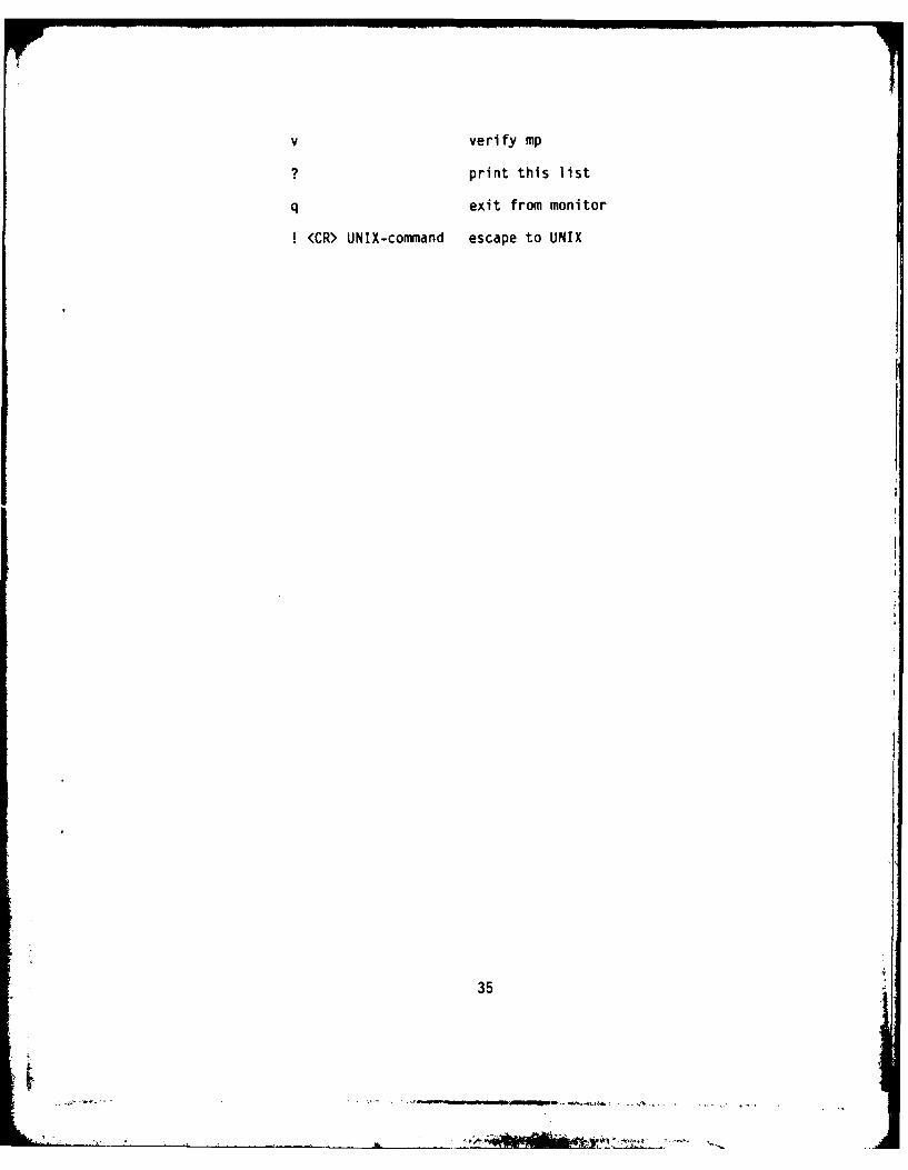
v verify mp
? print this list
q exit from monitor
(CR> UNIX-coninand escape to UNIX
35

APPENDIX C
SIMULATOR COMMAND DESCRIPTIONS
q quit
help
b [brkpt] [count] list or set breakpoint
d delete breakpoint
c continuous mode
<CR> single step mode
v view display
vm view multiplier
rr read ALU registers
wr reg# data write ALU register
rd addr [#read] read data memory
wd addr data write data memory
-rp addr [#read] read program memory
wp addr data write program memory
spc newpc set program counter
! <CR> UNIX-command escape to UNIX
vs view stack
sw [-] change w-switch status
sv [-) change v-switch status
va view ALU
vis view interrupt status
sic ctr set instruction counter
clk change clock
36

vt view timers
clri clear interrupt timers
rs t reset timers
37

APPENDIX D
INTERRUPT LOGIC EQUATIONS
Vo (3+rl72).-nt v0.int
int ie. (int-+d-i nt) (r 3 +r2 +r 1+r0)
dint:= int
S3 = (-i-efi nt -dint) -r3
S2 = ("ieslnt+dint).r2 + r3.r2 )r
si (iTe-ints-dint).rj + (r 3 +r24)rc
where rksk+irk, =,.3
and means equal after rising edge of clock
means logical AND
+ means logical OR
38

APPENDIX E
ALPCM SPECIFICATIONS
Cycle time: 100 ns
Basic Logic Family: TTL, with high-power Schottky where necessary incritical paths
Program Memory (ROM): 4Kx48 bits 6-Intel 3632(4Kx8)
Data Memory (ROM): 2Kx16 bits 2-Intel 3636 (2Kx8)
Data Memory (RAM): 2Kx16 bits 2-lDT 6116 (2Kx8)
Multiplier: AMD 29517
Basic CPE: 4-AMD 2901C (4-bit slice)
Microsequencer: AMD 2910 (12-bit address)
System Timing Controller: AMD 9513
Audio Conditioning: 12-bit A/D, D/A conversionSwitched capacitor 8th order elliptic prototype inputand output filters, Reticon 5609
Electrical: 115 VAC, 50-440 Hz, 40W power dissipation
Total DIP Count: 100 chips and carriers
Size: 4"x8"x18 1/4"
Weight: 10 lbs.
Construction Technique: One universal wire wrap-board
7"x16"
Center plane voltage
Two outside planes ground
r 39
,.i. ~

UN(LASSIFIEI)SECURITY CLASSIFICATION OF THIS PAGE (tr Aw. .. iEsmtd)
READ I%%TR ()%o%
REPORT DOCUMENTATION PAGE IEuti OF tMI.'I1% ; ORM
I. REPORT NURER GOVT ACCESSION No. 3. RECIPIET'S CATALOG NUMBERSD-T R .3 037 ni '4. TITLE faftd Subhitie) S. TYPE OF REPORT A PEIOD COVERED
A Programmable Voice Processor for Fighter Technical Report
Aircraft Applications 1. PERFORMING ON. REPORT SUMER
Technical Report 6537. AUTHORrs) S. CONTRACT OR GRANT NUUNER(a)
Edward M. Hofstetter. Elliot Singer and Joseph Tierney Fi9628-80-(-0002
S. PERFORMING ORGANIZATION MIE AND ADDRESS I. PROGRAM ELEMENT. PROJECT. TASKLincoln Laboratory. M.I.T. AREA & WORK UNIT NUMBERS
SProject Nos. 2283. 4111- 2264. 7820P.). Box 73 program Element Nos. 27417F. 28010Flexington, NIA 02173-0073 andI 334011
I I. CONTROLLING OFFICE AME AND ADDRESS 12. REPORT DATE
Air Force Systems (Gmnmand, USAF 18 August 1983
Andrews AFB 13. NUMBER OF PAGESWashington. DC 20331 46
14. MONITORING AGENCY NAME & ADDRESS (if different from Controlling Office) 15. SECURITY CLASS, (of this report)
Eleetronic Systems Division Unclassified
lanscom AFB. MA 01731 Ii.. DECLASSIFICATION DOWNGRADING SCHEDULE
IS. DISTRIBUTION STATEMENT (of this Report)
Approved for public release; distribution unlimited,
17. DISTRIBUTION STATEMENT (of the abjjract entered in Block 20. if different from Report)
I1. SUPPLEMENTARY NOTES
None
IS. KEY WORDS (Continue on rererse side if necesary and identify by black number)
bit-slice microprocessor vocoder evaluation microcodelinear predictive vocoding speech compression pipeline design
29. ABSTRACT (Continue on reveret side if nec.ssary and identify by block number)A flexible. high-speed digital voice processor has been designed for use in conjunction with the JTIDS communication
terminal to be installed for testing on board F-15 fighter aircraft and in Army JTIDS installati ims. The processor, known asthe Advanced Linear Predictive Microprocessor (ALP(M). has an architecture which is similar to that of its predecessor IIIbut contains significant improvements in speed. memory, and software development aids. The design includes an arith-metic section (four AMD 290IC bit-slice RALU's and an AMD 29517 16 X 16 multiplier), a doubly pipelined control path.and an I/O section based on a finite state machine implementation. Microcode development is enhanced by the presence ofan interactive debugging system consisting of a plug.in monitor board controlled from a host computer. The ALPKM is cap-able of implementing conventional 2400 bps LPC vocoders in real time and is sufficiently powerful to accommodate movesophisticated, compuiationally intensive algorithms should the extra performance they pro%ide he required in the scereF 15 operational environment.
O FORM 1473 EmOMO OF M NOV N 1s OeOLETE UNCLASSIFIEDI Jm 73 SECURITY CLASSIFICATION OF THIS PAGE (WA-. ftu Iok-*

ILMEI


