FINAL REPORT THE ESTABLISHMENT OF PROCEDURES FOR THE APPLICATION OF INFRARED TECHNIOUES FOR THE mHANCEMENT OF LARGE SCALE INTEGRATION (LSI) RnTABZLITY CONTRACT NO. NAS8- 25862 CONTROL DCN 1-0-60-00030 (IF) AND SI (IF) Prepared By Vanzetti Infrared & Computer Systems, Inc, Dedham, Massachusetts For National Aeronautics and Space Administration George C. Marshall Space Flight Center Marshall Space Flight Center Huntsville, Alabama 35812 . March 31, ! 971
Transcript
FINAL REPORT
THE ESTABLISHMENT OF PROCEDURES
FOR THE
APPLICATION OF INFRARED TECHNIOUES
FOR THE
mHANCEMENT OF LARGE SCALE INTEGRATION (LSI) RnTABZLITY
CONTRACT NO. NAS8- 25862
CONTROL DCN 1-0-60-00030 ( IF) AND S I ( IF)
Prepared By
Vanze t t i I n f r a r e d & Computer Systems, Inc ,
Dedham, Massachusetts
For
Nat ional Aeronautics and Space Administration
George C. Marshall Space F l i g h t Center Marshall Space F l i g h t Center
Huntsv i l l e , Alabama 35812 .
March 31, ! 971
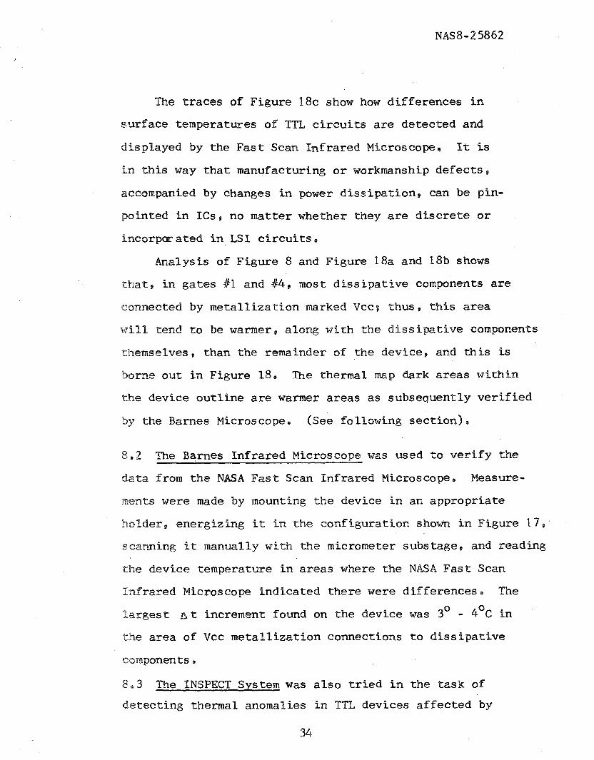
1 . INTRODUCTION
TABLE O F CONTENTS
2 0 PROBLEM D E F I N I T I O N
2.1 O X I D E DEFECTS
2e2 HANDLING AND OVERSTRESS
2 e 3 METALLIZATION AND P A R T I C L E
2.4 BOND AND CONNECTIONS
2 . 5 PACKAGE
2.6 PHOTOLITHOGRAPHY AND D I F F U S I O N
2.7 C H I P MECHANICAL
2.8 C H I P MOUNT
3 . PROGRAM OUTLINE
PAGE P
1
4 . COMPLEMENTARY CONTRACTOR 14
5 . TARGETS
6 . THE T E S T EOUIPMENT
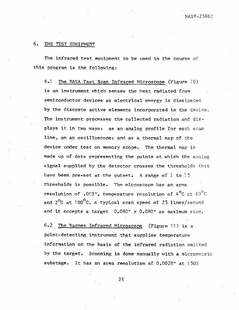
6.1 THE NASA F A S T SCAN INFRARED MICROSCOPE 21
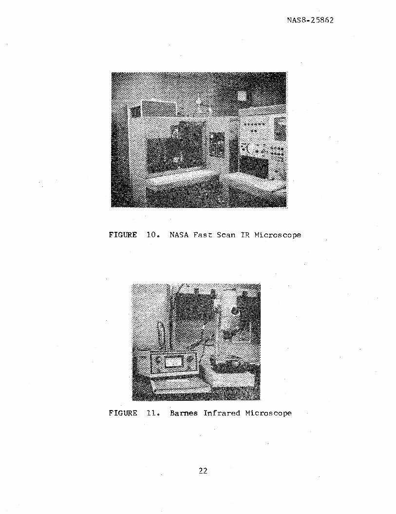
6.2 T H E BARNES INFRARED MICROSCOPE 21
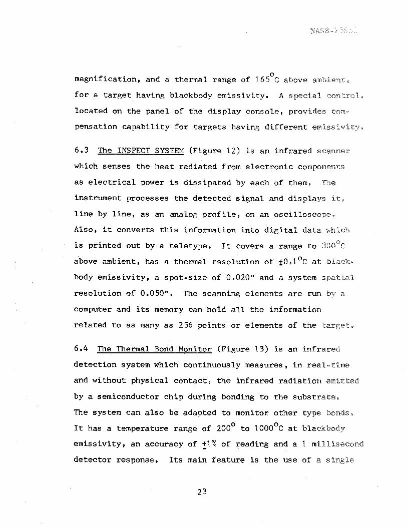
6 . 3 T H E I N S P E C T SYSTEM 23
604 T H E THERMAL BOND MONITOR 23
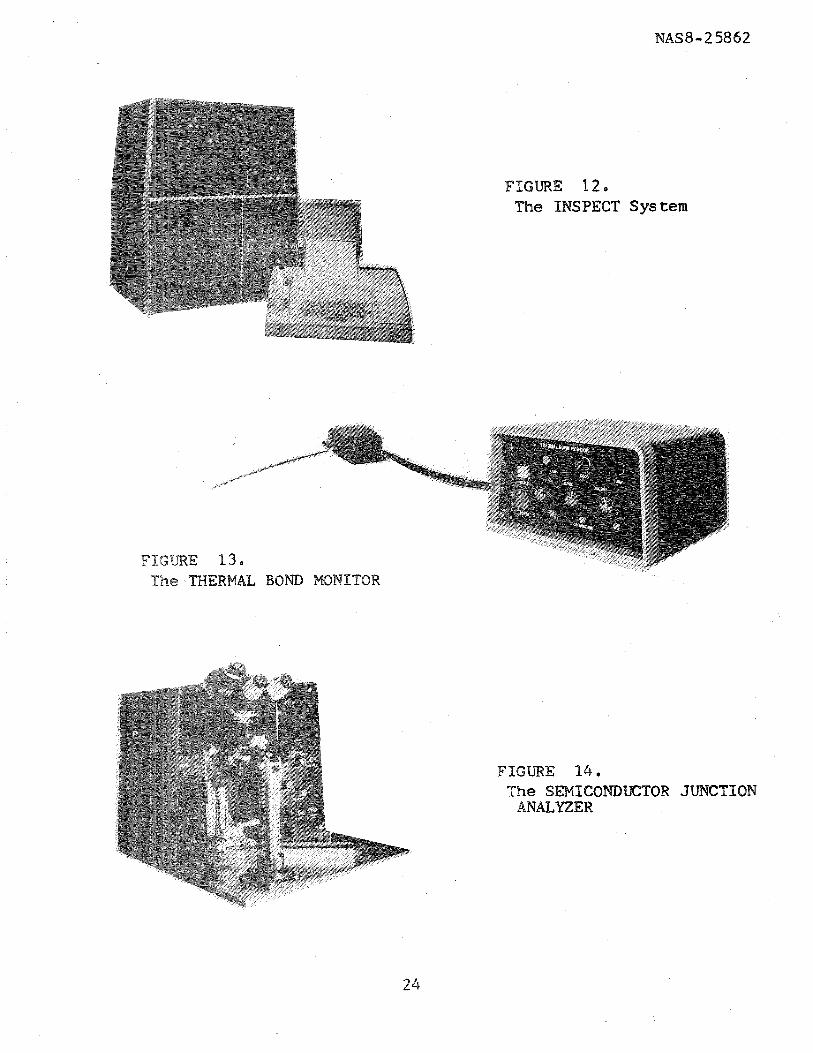
6 . 5 THE SEMICONDUCTOR JUNCTION ANALYZER 25
6 6 . MISCELLANEOUS EQUIPMENT 26
TABLE O F CONTENTS
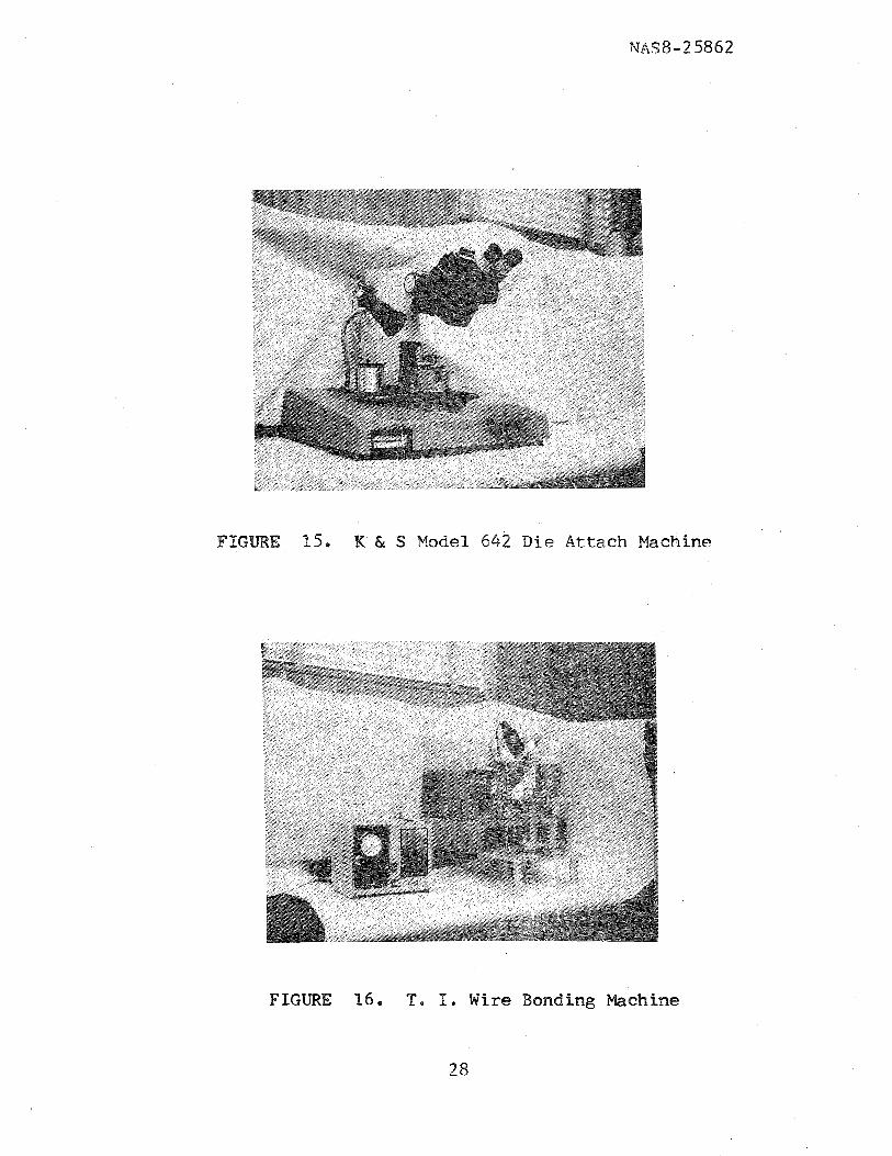
7 . THE THERMOCOMPRESSION BONDERS
7 . 1 DIE-ATTACH MACHINE
7.2 WIRE BOND MACHINE
PAGE -
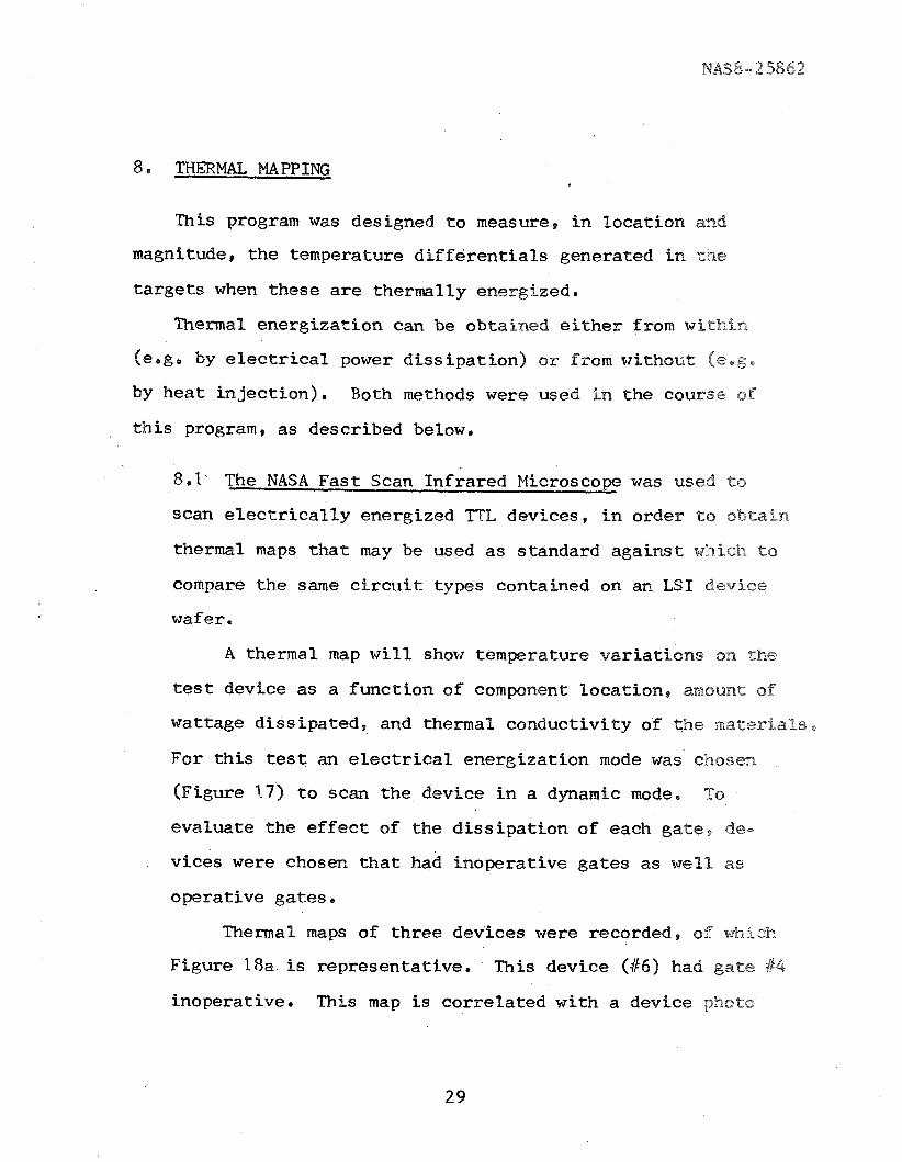
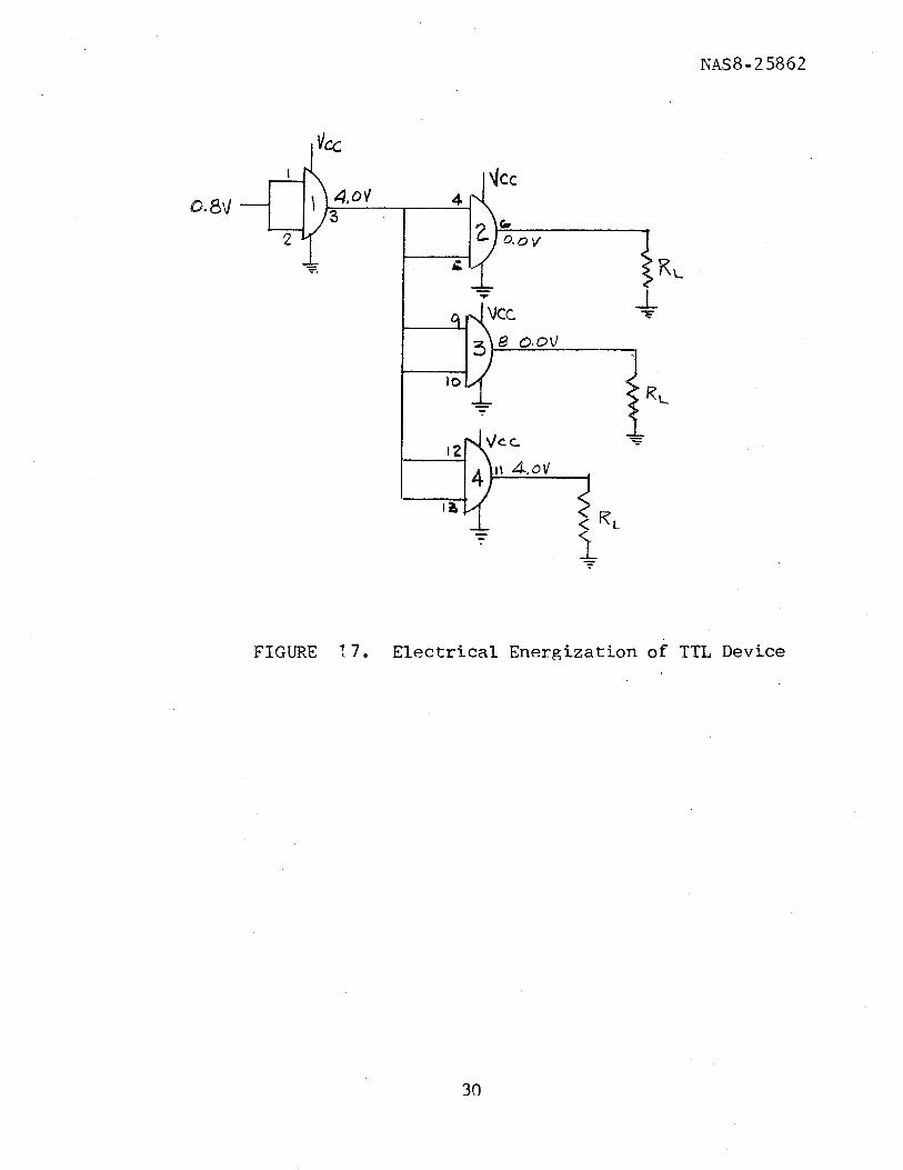
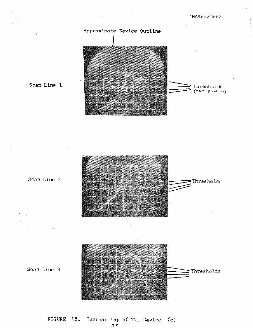
8, THERMAL MAPPING 29
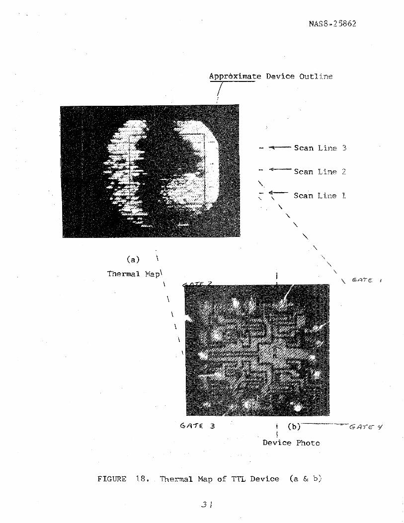
8,1 THE NASA F A S T SCAN INFRARED MICROSCOPE 29
8 , 2 THE BARNES I h F R A R E D MICROSCOPE 34
8 . 3 THE I N S P E C T SYSTEM
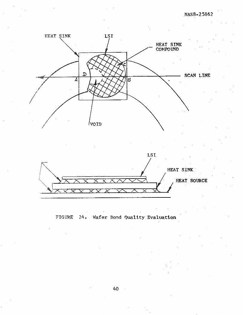
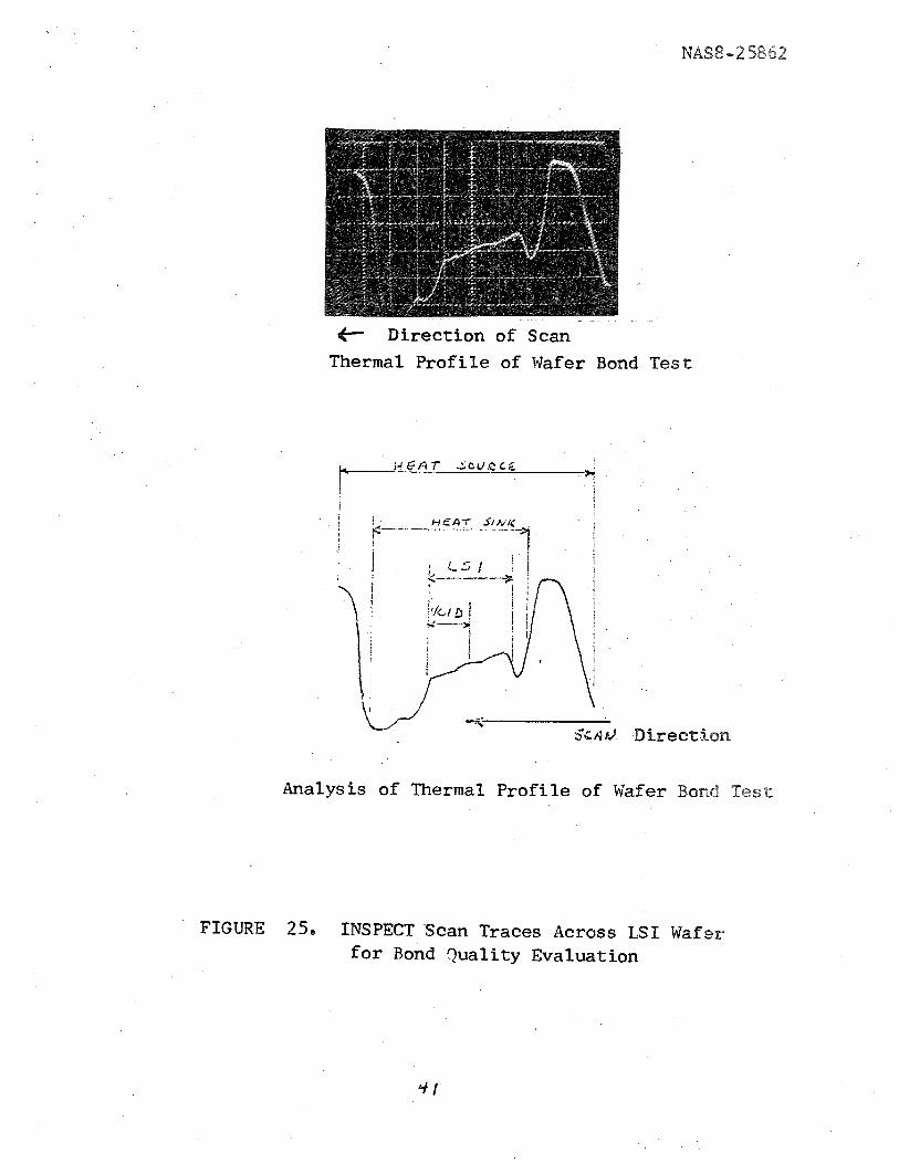
8m4 THE I N S P E C T SYSTEM - M E C H m I C A L R E J E C T L S I
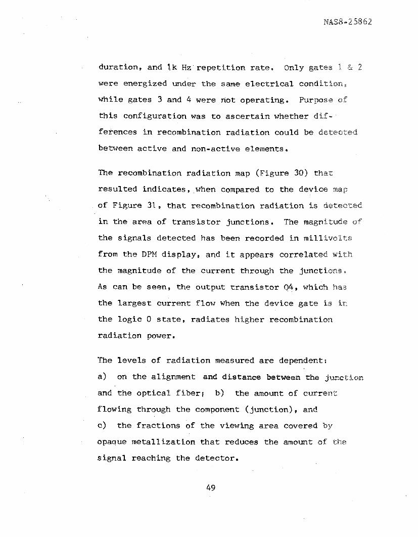
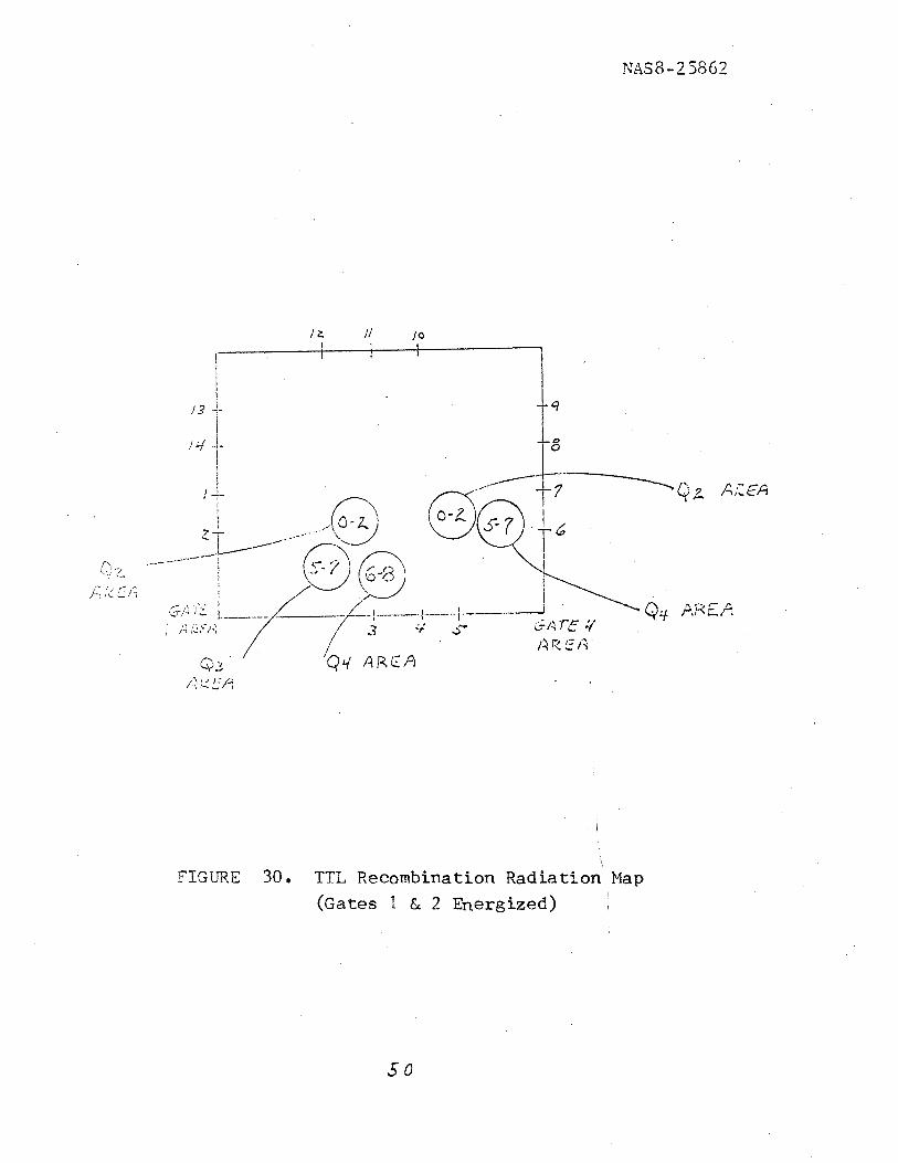
RECOMBINATION RADIATION STUDY
9,1 RECOMBINATION DATA O F CONTROL U N I T S
9m2 RECOMBINATION DATA O F T T L DEVICES
9m2.1 PHASE 1. F E A S I B I L I T Y PROGRAM
9.2 m I PHASE 2 m M E A S U R E F m T PROGRAM
9.3 RECOMBINATION DATA O F L S I UNITS
THERMOCOMPRESSION BONDING STUDY
10, l C H I P BONDING & MONITORING
10,2 WIRE BONDING &' MONITORING 87
10,3 USE O F THERMAL PROBE 91
10.4 RESULTS OF BONDING T E S T S 97
B 1 e CONCLUSIONS 98
TABLE OF CONTENTS
PAGE -
1 2. RECOMMENDATIONS 10%
12.1 LSI WAFER-SUBSTRATE BOND QUALITY EVALUATION 101
1202 CURRENT FLOW MEASUREMENTS THROUGH SEMICONDUCTOR JUNCTIONS 102
1203 WIRE BONDING PROCESS CONTROL
12.4 AREAS FOR LSI RELIABILITY ENHANCEMENT
12.5 REAL NUMBER RELIABILITY ENHANCEMENT 105
APPENDIX A
A FEASIBILITY STUDY OF A SCANNING HEAT INJECTION SYSTEM COUPLED WITH A SCANNING INFRARED DETECTION SYSTEM
iii
LIST OF ILLUSTRATIONS --
MOS FAILURE CAUSES
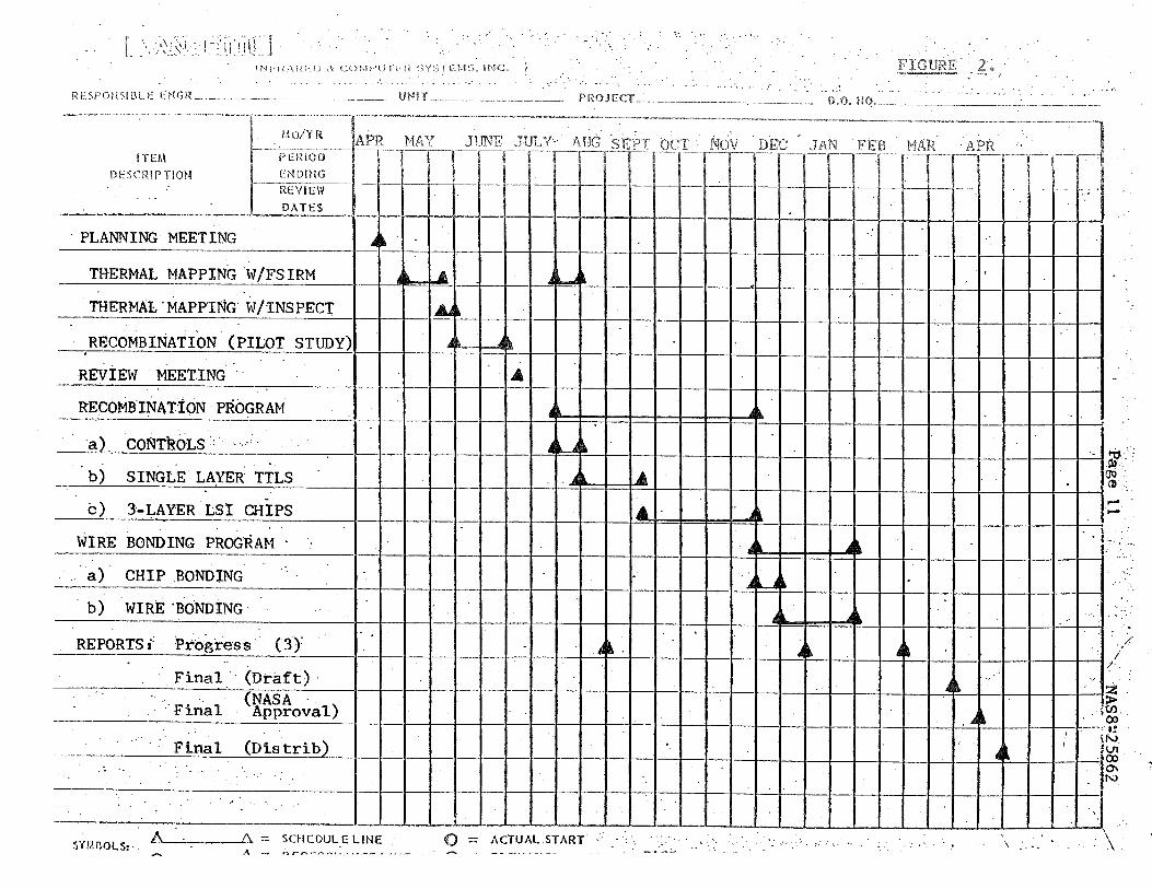
PROGRAM PLAN
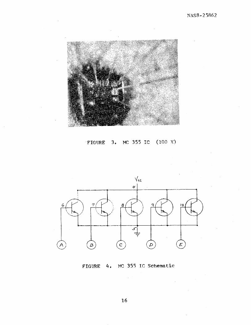
MC355 IC (VISIBLE PICTURE)
Me355 I C (SCHEMATIC)
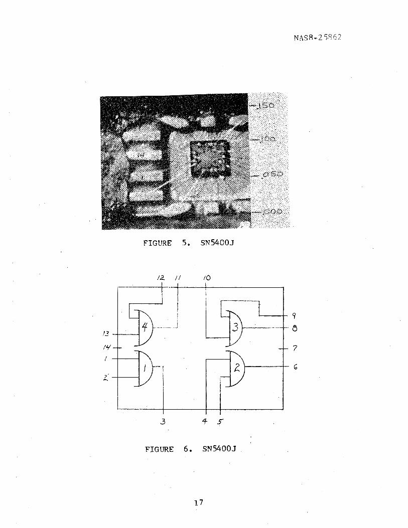
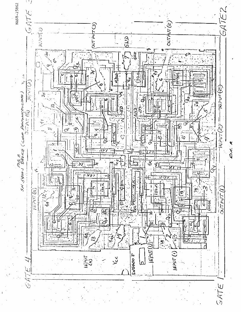
SN5400J DEVICE (VISIBLE PICTURE)
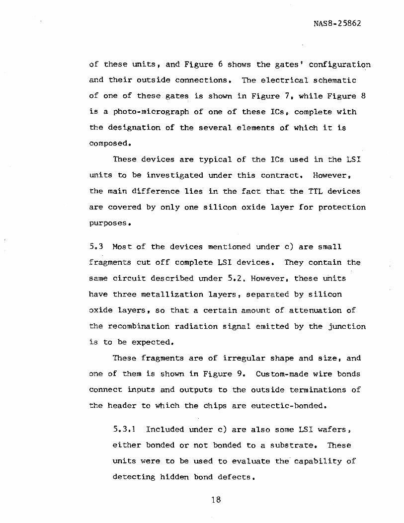
SN5400J DEVICE (GATES LAYOUT)
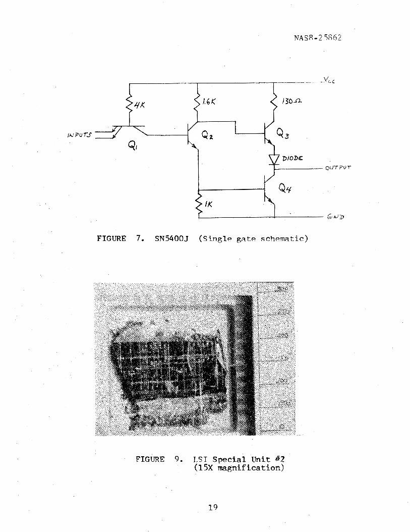
SN5400J DEVICE (SINGLE GATE SCHEWTIC)
SN5400J DEVICE (CHIP PHQTOMICROGRAPW)
L S I SPECIAL UNIT ?I2 (1 5X MAGNIFICATION)
NASA FAST SCAN INFRARED MICROSCOPE
BARNES INFRARED MICROSCOPE
THE INSPECT SYSTEM
THE THERMAL BOND MONITOR
THE SEMICONDUCTOR JUNCTION ANALYZE3
K & S MODEL 642 DIE-ATTACH MACHINE
TEXAS INSTRUMENT WIRE BOhqING MACHINE
PAGE - 3
LIST OF ILLUSTRATIONS (CONT WD)
PAGE
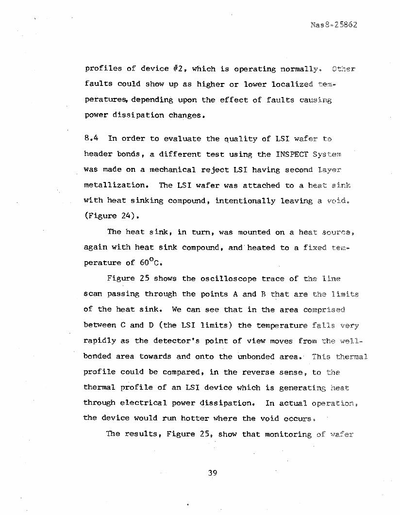
ELECTRICAL ENERGIZATION OF TTL DEVICE 30
THERMAL MAP OF TTL DEVICE 3 L & 33
ELECTRICAL ENERGIZATION OF TTL DEVICE FOR INSPECT TEST 36
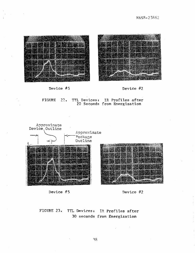
TTL DEVICES: I R PROFILES AT TIME 0
TTL DEVICES a I R PROFILES AFTER 20 SECONDS FROM EMERGIZATION 37
TTL DEVICES8 I R PROFILES AFTER 20 SECONDS FROM ENERGIZATION 38
TTL DEVICES: I R PROFILES AFTER 30 SECONDS FROM ENERGIZATION 38
WAFER BOND QUALITY EVALUATION 40
INSPECT SCAN TRACES ACROSS LSI WAFER FOR BOND QUALITY EVALUATION 41
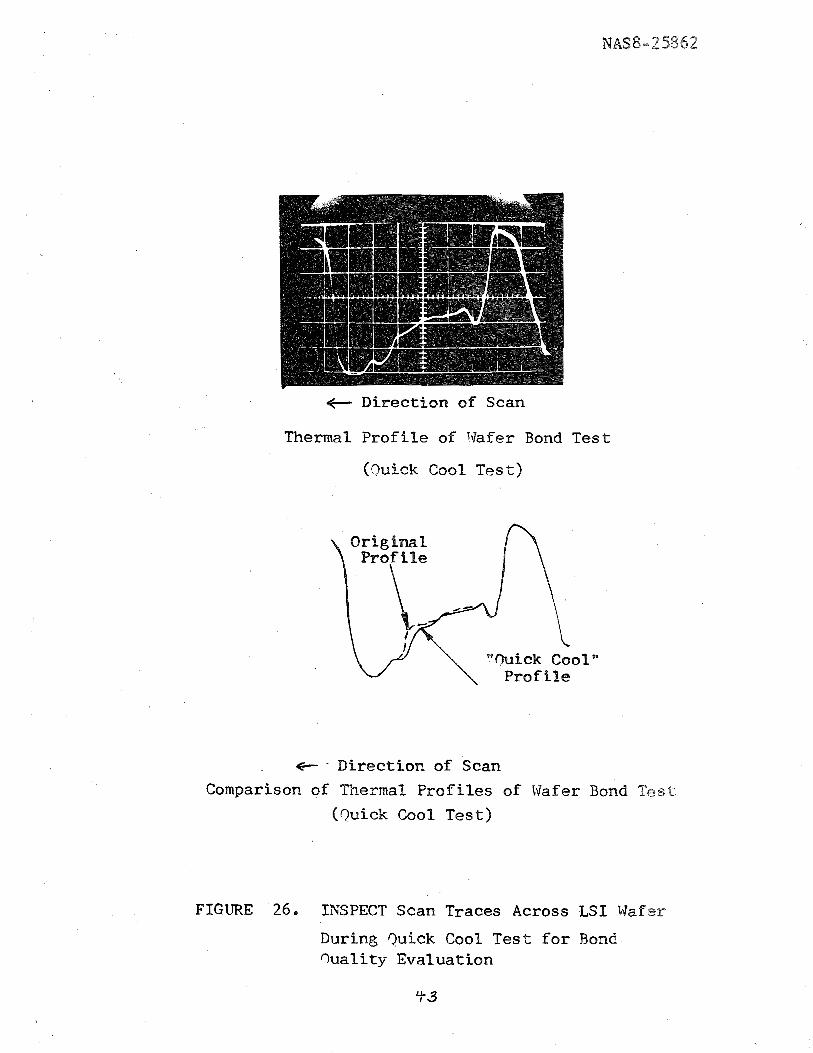
INSPECT SCAN TRACES ACROSS LSI WAFER DURING QUICK COOL TEST FOR BOND OUALITY EVALUATION 43
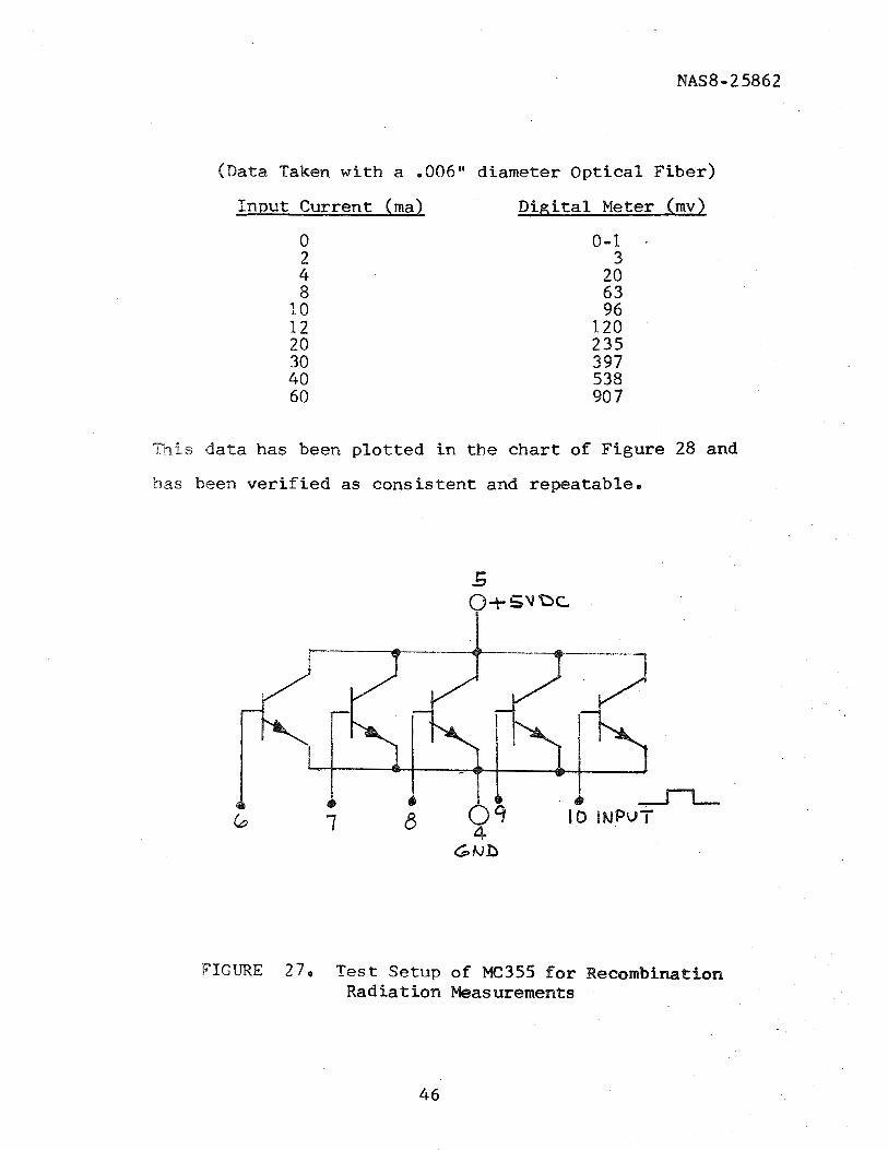
TEST SETUP OF MC355 FOR RECOMBINATION RADIATION MEAS UREMENTS 46
RECOMBINATION RADIATION VS DEVICE INPUT CURRENT 47
TEST .SETUP OF TTL DEVICES FOR PHASE 1 RECOMBINATION RADIATION STUDY 48
LIST OF ILLUSTRATIONS (CONTW)
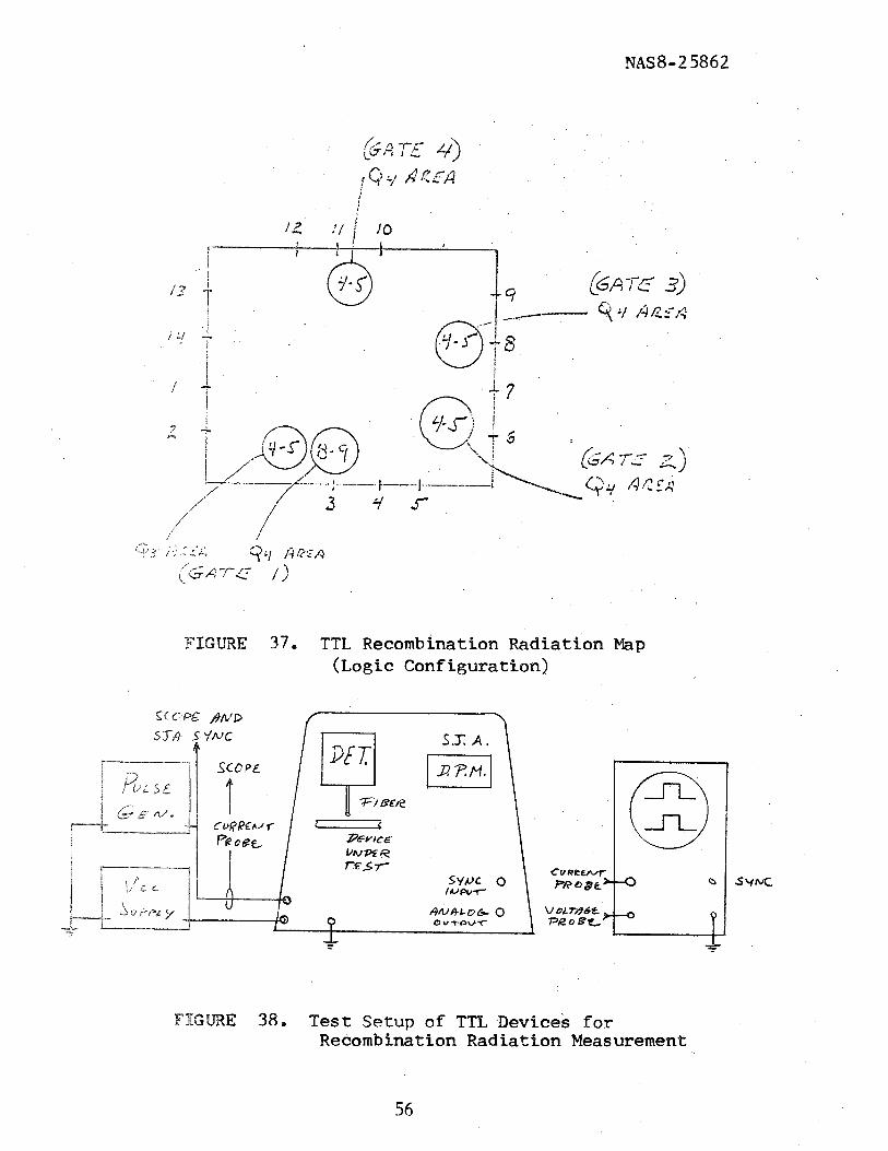
30, TTL RECOMRINATION RADIATION MAP 50
3 1 . JUNCTIONS OF GATES 411 and 2 IWESTIGATED FOR RECOMBINATION RADIATION 51
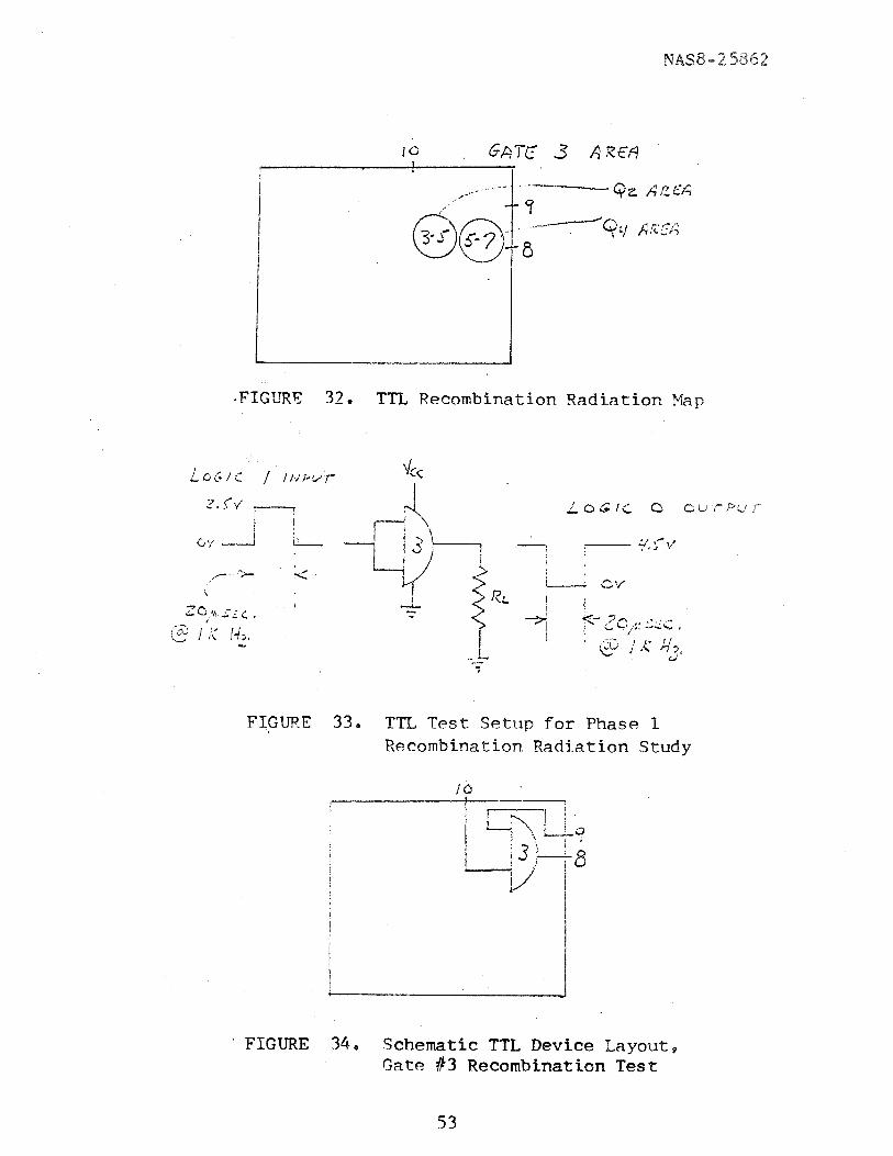
32, TTL RECOMBINATION RADIATION M P 53
3 3 . TTL TEST SETUP FOR PHASE 1 RECOMBINATION RADIATION STUDY 53
34, SCHEMATIC TTL DEVICE LAYOlJT, GATE i'j3 RECOMRINATION TEST 53
3 5 , JUNCTIONS OF GATE $3 INVESTIGATED FOR RECOMBINATION RADIATION 54
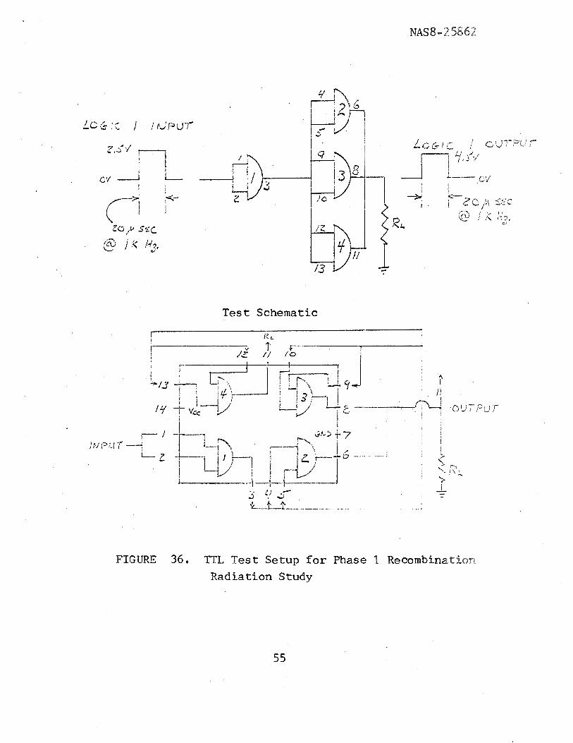
36, TTL TEST SETUP FOR PHASE 1 RECOMBINATION RADIATION STUDY 55
FIGURE 38. Test Setup of TTL Devices for Recombination Radiation Measurement
9.2.1.3 The evidence obtained through t h e above-
descr ibed tests l e d t o t h e conclusion t h a t it i s
indeed poss ib le t o d e t e c t and measure recombination
r a d i a t i o n emi t ted by semiconductor junct ions of
i n t e g r a t e d c i r c u i t s of TTL type.
Phase 1. was t h e r e f o r e considered suceessf ully
completed, so t h a t Phase 2 could be i n i t i a t e d on the
bas is of t h e prel iminary p o s i t i v e evidence gathered
i n Phase I .
9,2.2 Phase 2. Measurement Program
The TTL devices , a l ready descr ibed i n 5 ,2 , were
e l e c t r i c a l l y energized as i l l u s t r a t e d i n Figure 38;
namely, t h e g a t e under tes t would he operated as
fol lows: a p o s i t i v e vol tage pulse w a s app l i ed t o t h e
input te rminal a t 1 K Hz r e p e t i t i o n r a t e and 20 pet,
pulse width, This pulse serves two purposes, It
opera tes t h e g a t e a t a low (2%) duty cyc le and it gates
t h e Semiconductor Junct ion Analyzer e l e c t r o n i c s 870
"look" a t t h e de tec ted si,gnal on ly when t h e test device
has switched from Logic 1 t o Logic 0. The outputs were
n o t loaded f o r these tests, and ga tes 1 t o 4 w e r e energized
one a t a t i m e , a s noted i n each set of d a t a .
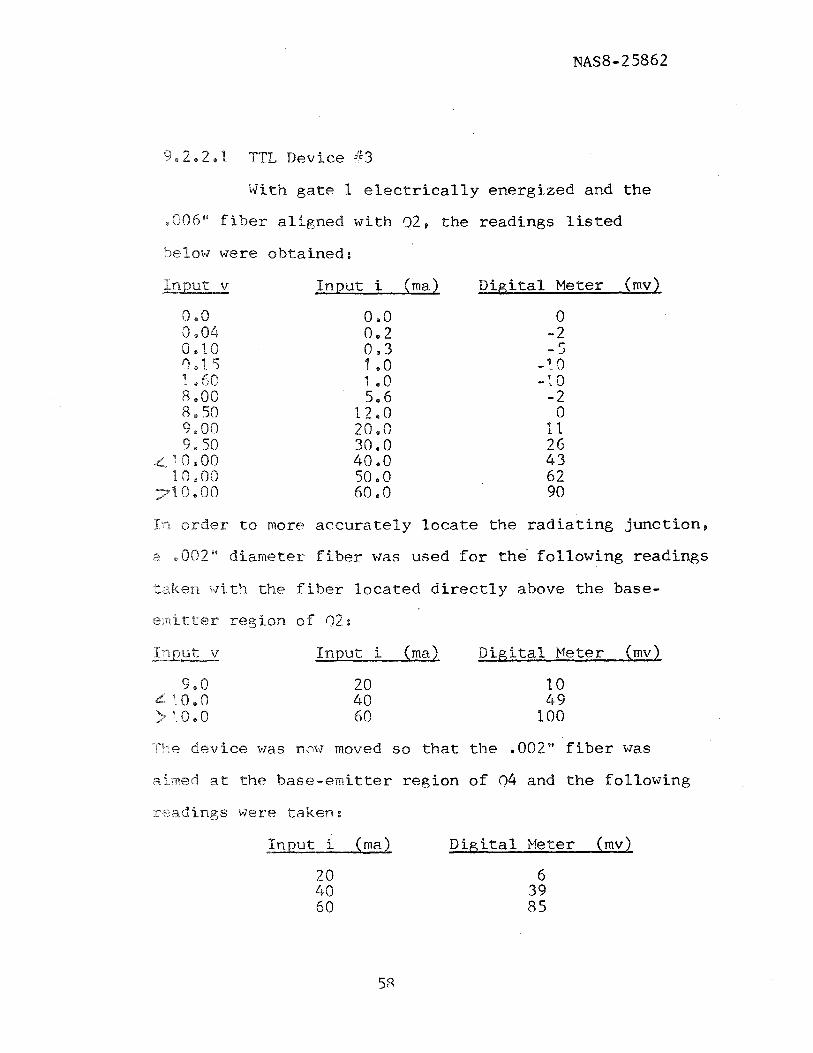
9,2,2,1 TTL Device $3
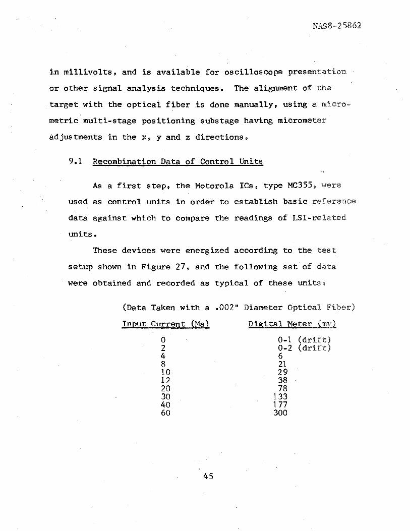
With g a t e 1 e l e c t r i c a l l y energ ized and t h e
,006" f i b e r a l igned w i t h 92, t h e readings l i s t e d
below w e r e ob ta ined:
Input i (ma) D i g i t a l Meter (mv)
In o r d e r t o more a c c u r a t e l y l o c a t e t h e r a d i a t i n g junc t ion ,
2 .002" diameter f i b e r was used f o r t h e fo l lowing read ings
taken w i t h t h e f i b e r l o c a t e d d i r e c t l y above t h e base-
e m i t t e r reg ion of Q2r
Input i (ma) D i g i t a l Meter (mv)
T h e dev ice was nnv moved s o t h a t t h e .002" f i b e r was
a imed a t the base -emi t t e r reg ion of 04 and t h e fo l lowing
readings were taken:
D i g i t a l Meter (mv)
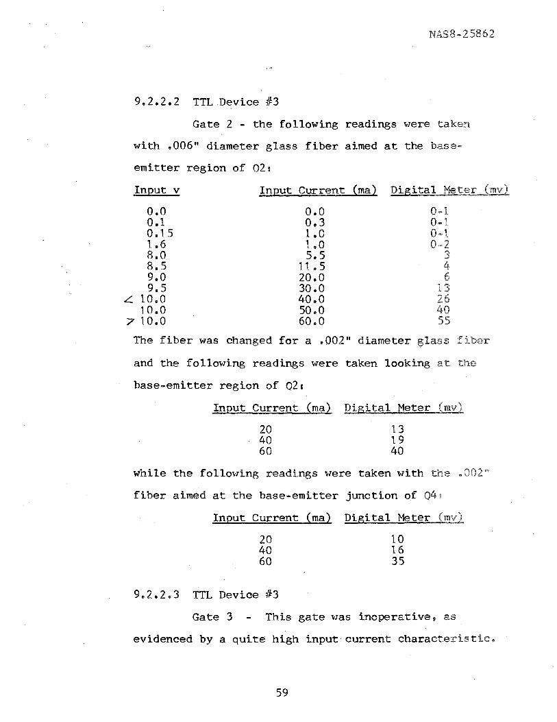
9.2.2.2 TTL Device #3
Gate 2 - t h e following readings w e r e taken
with .006" diameter g l a s s f i b e r aimed a t the base-
emitter region of 02:
Input v Input Current (ma)
The f i b e r w a s changed f o r a .002" diameter g l a s s f iber
and t h e following readings w e r e taken looking a t the
base-emi t te r reg ion of 028
Input Current (ma)
while t h e f o l l o v ~ i n g readings w e r e taken w i t h . t h e eO0289
f i b e r aimed a t t h e base-emi t te r junct ion of 048
Input Current (ma)
9.2.2.3 TTL Device 8 3
G a t e 3 - This g a t e was inopera t ive , as
evidenced by a q u i t e high inpu t c u r r e n t c h a r a c t e r i s t i c ,
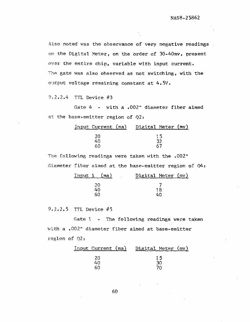
Also noted was t h e observance of very negat ive readings
on t h e D i g i t a l Meter, on the o rde r of 30-40mv, present
over the e n t i r e chip, v a r i a b l e with input cu r ren t ,
The g a t e w a s a l s o observed as n o t switching, with t h e
output vol tage remaining cons tant a t 4,5V.
9,2.2.4 TTL Device
Gate 4 - with a ,002" diameter f i b e r aimed
a t the base-emit ter region of Q2r
Input Current ( m a ) D i g i t a l Meter (mv)
The following readings were taken wi th t h e .002"
diameter f i b e r aimed a t t h e base-emit ter region of 048
Input i (ma) D i g i t a l Meter (mv)
9,2,2.5 TTI, Device $5
Gate 1 - The following readings w e r e taken
with a ,002" diameter f i b e r aimed a t base-emi t te r
region of 92:
Input Current (ma) D i g i t a l Meter (mv)
Then with t h e s,ame ,002" f i b e r aimed a t base-emitter
region of 048
Input Current (ma)
9.2,2,6 TTL Device /I5
Gate 2 - The following readings w e r e t aken
with a .002" diameter f i b e r aimed a t base-emitter
region of 021
Input Current (ma)
Then with the same ,002" f i b e r aimed a t base-emitter
region of 04:
Input Current (ma)
9.2e2.7 TTL Device #5
Gate 3 - This ga t e was inoperative. The
cha rac t e r i s t i c s w e r e very similar t o TTL #3 , Gate 3 ,
insofar as very high input current and constant oiu"tgpaat
voltage.
9.2.2.8 TTL Device #5
Gate 4 - This ga t e was inoperat ive with
observations s imi l a r t o the ones described i n 9 , 2 , 2 , 7 above,
9,2 .2 ,9 A t t h e conclusion of t h i s work, a l l d a t a
obtained was eva,luated f o r r e p e a t a b i l i t y and consis tency,
Following s a t i s f a c t o r y v e r i f i c a t i o n of t h e above charac-
t e r i s t i c s , t h e r ad ia t ion-cur ren t c o r r e l a t i o n curves of
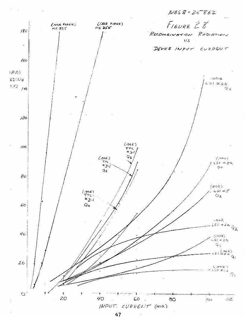
02 and 04 of g a t e !bI, TTI, u n i t # 3 , were p l o t t e d on t h e
c h a r t of Figure 28, a s t y p i c a l of t h i s fami ly of semi-
conductor devices .
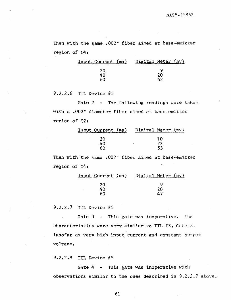
9 , 3 Recombination Data of LSI Units
These devices have been descr ibed i n Sec t ion 5.3 (See
F igu re 9 ) They w e r e t o be e l e c t r i c a l l y energized as
shown in Figure 29, s o a s t o have them opera t ing i n t h e
same mode a s t h e TTL u n i t s a l r eady measured, In t h i s way,
the effect of t h e a d d i t i o n a l m e t a l l i z a t i o n l a y e r s could be
evaluated,
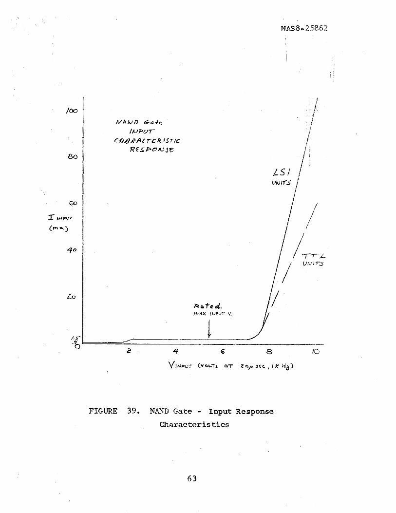
'This approach is f u r t h e r j u s t i f i e d by t h e comparison
of the input c h a r a c t e r i s t i c s of the two f a m i l i e s of devices ,
These are shown i n Figure 39, and they show coincidence up
t o the "avalanche knee", After t h i s po in t , t h e two curves
show some divergence, although s t ill r e t a i n i n g a l i n e a r
behavior. Since t h e s e " spec ia l u n i t s " have been c u t o f f
completed and opera t ive LSI c i r c u i t s , a success fu l test
program ~r~ou ld automat ica l ly prove the f e a s i b i l i t y t o measure
current flow a t any junct ion of LSI u n i t s .
W A N D Ga4e
/ n / p u r
CH&RAc rt: R J Srlc
FIGURE 39. NAND Gate - Input Response
Character is tics
FOI~JE" of these " s p e c i a l u n i t s " were suppl ied by Texas
Instruments f o r eva lua t ion , These devices contained various
""verified opera t iona l " mul t ip le- input ga tes with schematic
as sklocm i n Figure 7 , except for the number of inputs , The
v z r i a t i o n i n number of inputs merely makes each of t h e f o u r
devices d i f f e r e n t i n layout and meta l l i za t ion pa t t e rns . A s
far as opera t iona l c h a r a c t e r i s t i c s a r e concerned, t h e LSI
devices and t h e TTL u n i t s a r e the same, by design. I n
p a r t i . e u l a r , u n i t s 2 2 and -46 have two ga tes each, while
u n i - t ~ iL4 and 85 have one g a t e each. Figure 9 and Figure 40
to 53 show rhe v i s i b l e p ic tu res of these u n i t s , taken a t
various magnif icat ion f a c t o r s , and t h e i r e l e c t r i c a l schematics.
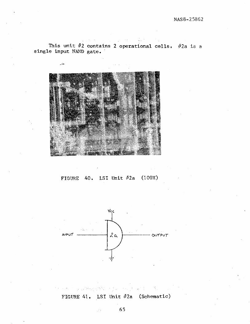
This u n i t 8 2 contains 2 operat ional cells. #2a is a s i n g l e input NAND gate. '
FIGURE 40. LSI Unit #2a (100X)
FIGURE 42, LSI Unit #2a (Schematic)
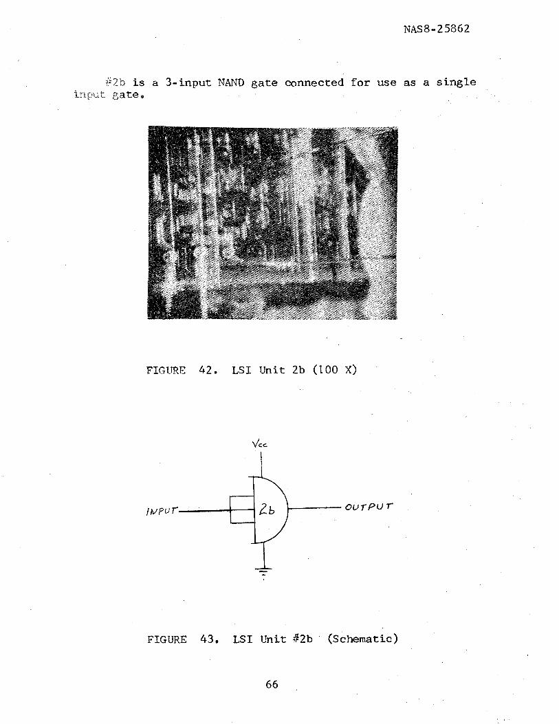
i12b is a 3-input NARD ga te connected f o r use a s a single input gate ,
FIGliRE 42. LSI Unit 2b (100 X)
FIGURE 4 3 , LSI Unit #2b (Schematic)
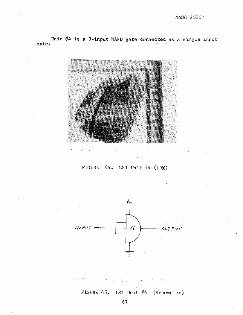
Unit #4 is a 3-input NAND gate connected as a s i n g l e inpu t g a t e ,
FIGURE 4 4 , LSI Unit 94 ( 1 5 ~ )
FIGURE 45. LSI Unit /I4 (Schematic)
67
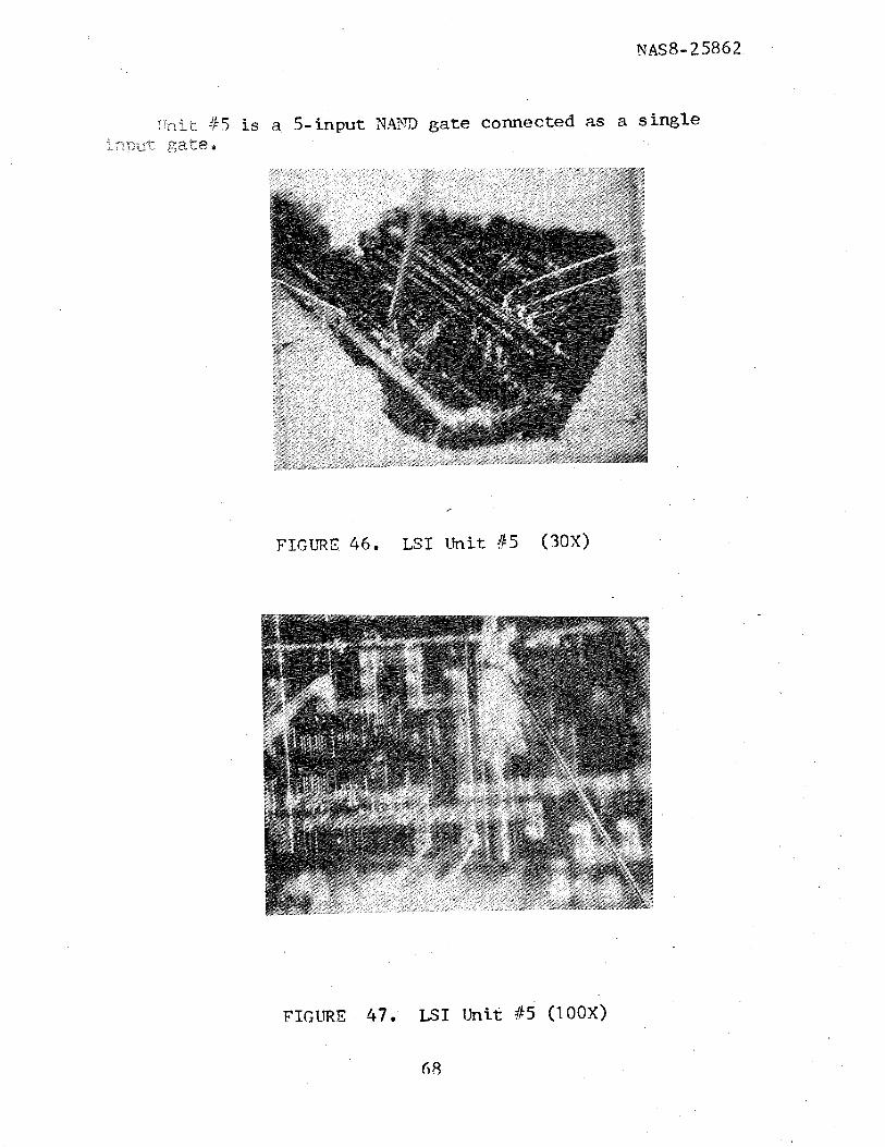
iVn i t 65 is a 5-input 4 G t D gate connected as a s ing le LnpuCgate,
FIGC'RF 46. LSI Unit $5 ( 3 0 X )
FIGURE 47. LSI IJnit 7'b5 (IOOX)
68
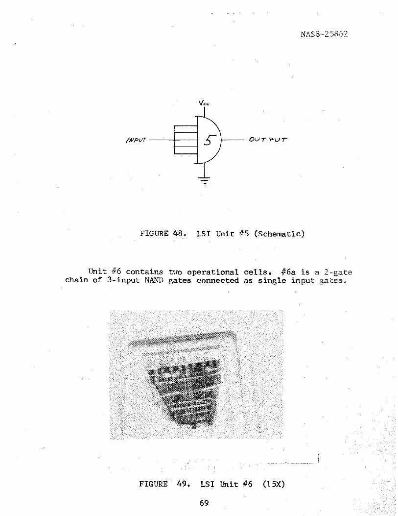
FIGURE 48. LSI U n i t !!5 (Schematic)
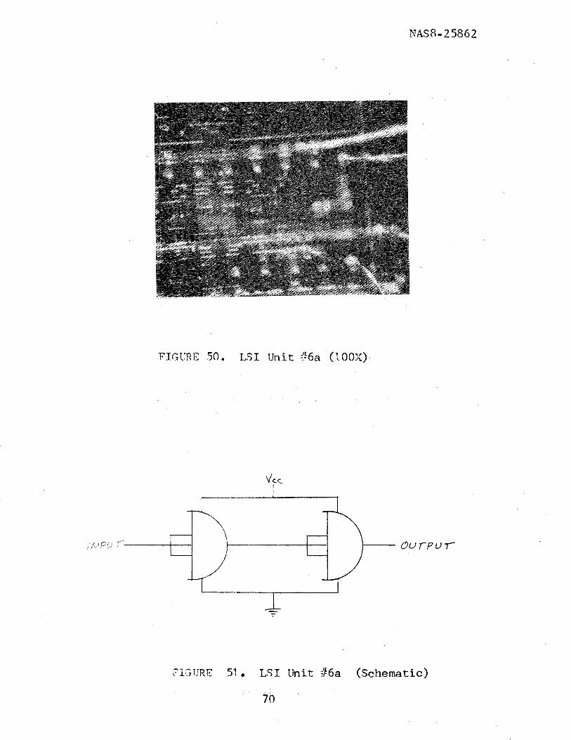
Unit !I6 contains nlro operational ce l l s , #6a i s a 2-gate chain of 3- input NAYD gates connected as single input gates,
FIGURE 4 9 , LSI Unit !F-6 ( 1 5 ~ )
69
FIGITRE 50. L.SI Unit 56a (100);)
,- -- ,-. i. L ~ J ~ J R F 51 , LSI l Jn i t :F6a (Schematic)
70
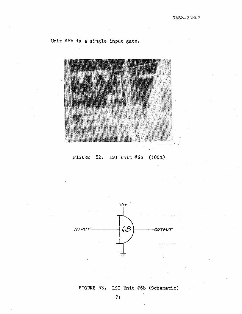
Unit #6b is a s i n g l e input gate.
I . . -- - -- - -
FIGURE 52. L S I IJnit #6b (IOOX)
v c c
FIGUICE 53. L S I Unit #6b (Schematic)
71
ESI "Special Unit" 42a
The following d a t a was taken t r i th a ,006"
diameter g l a s s f i b e r looking a t 04. The input charac-
t e r i s t i c w a s v e r i f i e d as conforming t o Figure 39,
Input Voltage
0 1.5 6.5 7.0 7.5 8.0 8.5 9.0 9.5
20.0 10,o 10.0
The f i b e r was replaced wi th a .002" f i b e r f o r t h e
following readings , looking a t Q4:
Input Current (ma)
1.6 8.0
10.0 20 .o 40 .O 60.0 80.0
100.0
D i g i t a l Meter (mv)
I 1-2 3 6
10 18 26 39
Then looking a t Q2 wi th t h e .002" f i b e r , t h e r e was no
r a d i a t i o n v i s i b l e s i n c e t h e base-emit ter region is
covered with me ta l l i za t ion .
9 . 3 , 2 LSI "Special uni tW#2b
I n i t i a l a t tempts t o l o c a t e a r a d i a t i n g junction
w e r e n o t very success fu l , al though t h e input @hasac-
t e r i s t i c w a s v e r i f i e d and t h e r e w a s an i n d i c a t i o n of
r a d i a t i o n from t h e base-emi t te r region of 94, bu t wi th
a .006" diameter f i b e r , t h e r a d i a t i o n could not be
"peaked" due t o the presence of a l ead w i r e , The fiber
was replaced w i t h a ,002" diameter f i b e r with the fol-
lowing readings taken, looking a t t h e base-emit ter
reg ion of 04%
Input Current ( m a )
No r a d i a t i o n was observed from 42 o r o t h e r components,
Q2 was covered with gold me ta l l i za t ion .
9.3.3 LSI "Special Unit" #4
This u n i t w a s n o t opera t ing properly. Only G rn;,
of Pnput curren.? '?as obtained a t maximum input voltage
and a t t h a t l e v e l no r a d i a t i o n was evident . The o u t p u t
V remained p o s i t i v e a t a l l times.
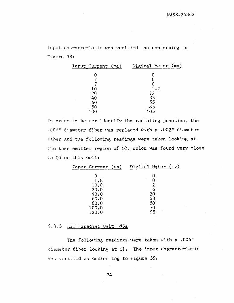
9.3.4 LSI "Special Unit" 4 6
The following readings were taken with a a006n'
diameter f i b e r looking a t the v i . c in i ty of 03, The
i n p u t c h a r a c t e r i s t i c was v e r i f i e d a s conforming t o
F igure 39;
Input Current (ma) D i g i t a l Meter (mv)
In o r d e r t o b e t t e r i d e n t i f y t h e r a d i a t i n g junct ion , t h e
.306" diameter f i b e r was replaced wi th a .002" diameter
Tibcr and the following readings were taken looking a t
the base-emi t te r region of 0 2 , which was found very c l o s e
t o Q3 on t h i s c e l l :
Input Current (ma) D i g i t a l Meter (mv)
9,3, F-, LSI "Special Unit" IF6a
The f o l l o t ~ i n g readings were taken wi th a ,006"
diameter f i b e r looking a t 01. The input c h a r a c t e r i s t i c
was v e r i f i e d as conforming t o Figure 39:
Input Current (ma)
In order t o i den t i fy t he radia t ing junction, t h e .006"
diameter f i b e r was replaced with a .002" diameter f iber
and the following readings w e r e taken, looking a t QI :
Input Current (ma)
The following readings w e r e also taken on lJnFt /&a a.fter
ident i fy ing the junctions shotm:
Input Current (ma)
Q2 (b-e)
3s rad ia t ion was v i s i b l e from 2nd gate of Unit #6a s ince
most sf c e l l is covered with meta l l iza t ion,
9,3,6 L S I "Special Unit" #!6b
The following readings w e r e taken with a .006"
diameter f i b e r looking a t Q4, The input c h a r a c t e r i s t i c
was ver i f i ed as conforming t o Figure 398
Input Current (ma) Dig i ta l Meter (rnv)
In order t o i den t i fy the junction, the ,006" diameter
f i b e r was changed t o a .002" diameter f i b e r and the
fol lowing readings were taken when looking a t base-
emitter region of 0 4 ;
Input Current (ma) Dig i ta l Meter (mv)
There was no rad ia t ion evident a t 42 s ince the junction
bras covered by metal l izat ion.
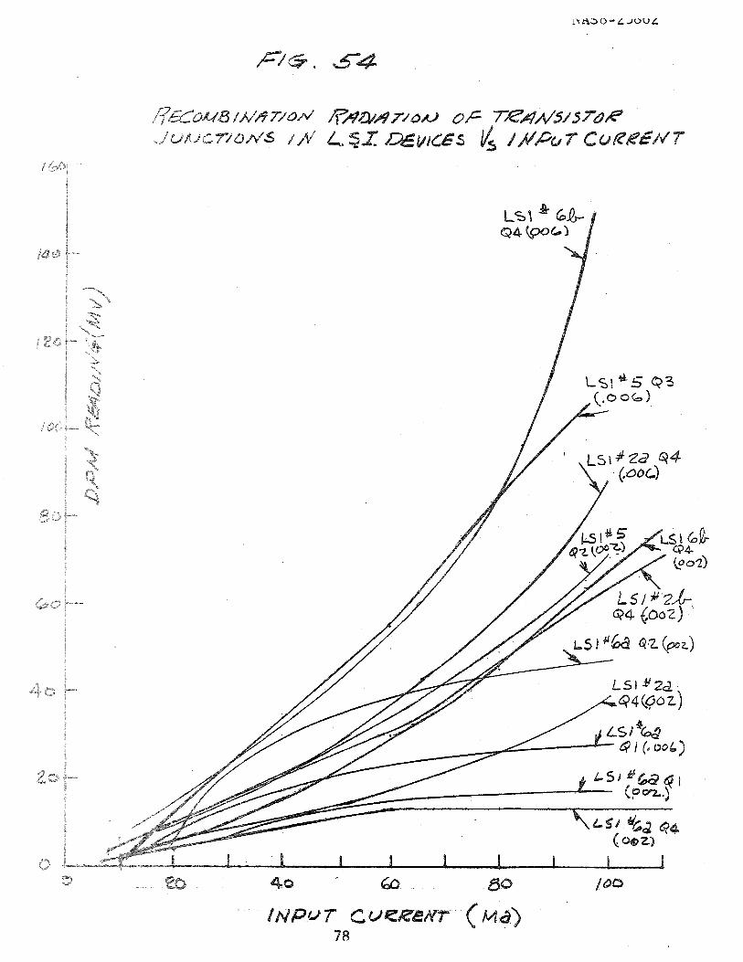
9.3.7 A t t h e conclusion of t h i s work, a l l d a t a obtained
was reviewed f o r r e p e a t a b i l i t y , cons is tency , and cor-
r e l a t i o n with t h e da ta obtained from t h e TTL devices,
The L S I da ta w a s p l o t t e d i n the c h a r t of Figure 54, and
it became apparent t h a t t h e response of u n i t /%a is
d i f f e r e n t from the response of a11 o t h e r units, This
divergence of t h e r a d i a t i o n c h a r a c t e r i s t i c of LSI u n i t
#6a from t h e genera l shape of t h e o t h e r u n i t curves
could n o t be explained, Tes ts were made pu t t ing o t h e r
ga tes i n t o the same e l e c t r i c a l conf igura t ion , but no
change of t h e r a d i a t i o n c h a r a c t e r i s t i c s of t h e other
u n i t s took place. Therefore, it appears a s if the odd
c h a r a c t e r i s t i c of Unit F6a is an i n t r i n s i c feature of
t h a t u n i t , and does not depend on the e l e c t r i c a l eon-
f i g u r a t i o n of t h e c i r c u i t r y . A r a t h e r p l a u s i b l e
hypothesis is t h a t i-t might be caused by anomalies in
t h e forbidden gap of t h e semiconductor ma te r i a l where
t h e junct ions a r e loca ted ,
With t h e except ion of Unit #6a, t h e response of'
t h e LSI u n i t s shot:s s a t i s f a c t o r y c o r r e l a t i o n w i t h the
response of t h e TTL devices . For comparison purposes,
the r a d i a t i o n - c u r r e n t c o r r e l a t i o n curves of L S I un i t s
#2a, 5 and 6b have been p l o t t e d on t h e c h a r t of Figure 28,
t oge the r with those of IJnit Ib6a which shows t h e anomalous
devia t ion .
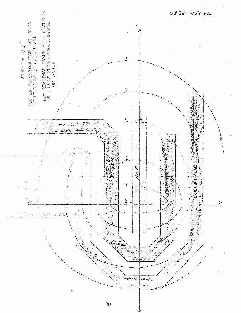
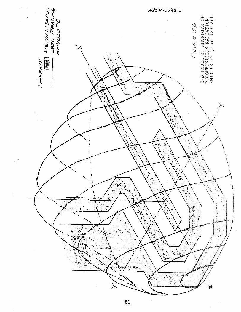
9.3.8 In order t o f ind out what e f f e c t the metal-
l i z a t i o n has on the shape of the emitted rad ia t ion ,
the base-emitter junction of Q4 of LSI un i t #6b was
se lec ted f o r area and contour measurements,
The data s o generated w a s p lo t ted f i rs t in a
map configurat ion, and then a three-dimensional. moldel
was derived, as i l l u s t r a t e d i n Figures 55 and 56,
Some asymmetry is apparent, evidently due t o the
d i f f e r e n t shape of the meta l l iza t ion i n the various
areas around the junction,
TtISRklOCOMPRESSION RON-DING STUDY --
"I3nsc. goLaPs of t h i s program were t o i n v e s t i g a t e tqhether
i>?f rared t e c b i q u e s could be use fu l 8
d'$ t o assess t h e q u a l i t y of t h e w i r e bonds connecting
the LSI wafer t o t h e ou t s ide package te rminat ions ,
o r preferably,
" f ) t o monitor t h e wire bonding opera t ion so as t o
assure and con t ro l the good q u a l i t y of t h e w i r e
bonds while they are being performed*
major var iab les a f f e c t i n g the q u a l i t y of semiconductor
I i?e bo7nds are the following :
\ ceollet pressure
2, c o l l e t temperatwe
3, chip temperature
* c h i p b e a t s inking -+ *
5, c l ean l iness of sur faces t o be bonded
31 these v a r i a b l e s , only those r e l a t e d t o temperature could
de ~ o n k t o r e d with the i n f r a r e d t e s t equipment a t our d i sposa l .
1.9 e f f o r t was made t o keep t h e bonding pressure cons tan t , and
ro avo id contamination of khe su r face of the elements t o be
bonded,
The vire bonding machine used was shown i n Figure 16, The
.ale w i r e used throughout t h i s work was 0.0007" i n diameter , r
and s e v e r a l c o l l e t s f o r t h i s s i z e w i r e w e r e suppl ied by Texas
Instrument, Extreme d i f f i c u l t y w a s m e t i n threading the gold
w i r e through the c o l l e t . Fur the r problems w e r e caused by
w i r e clogging i n t h e c o l l e t " o r i f i c e , A l l t h i s caused a
tremendous amount of t i m e l o s t i n opera t ion s e t u p and per-
formance, t o the e x t e n t t h a t only a l i m i t e d number of \rise
bonds could be considered usable f o r t h e program,
Temperature s t a b i l i t y measurements, both of t h e e o l l e t
and of t h e s u b s t r a t e (pad) , w e r e taken wi th s i g n i f i c a n t results
t h a t are descr ibed i n Sec t ion 10,3.
A s a prel iminary s t e p , a number of semiconductor ch ips
w e r e needed, on which w i r e bonds w e r e t o be appl ied . I t w a s
thought important t o know t h e q u a l i t y of t h e bond beDaeen c h i p
and s u b s t r a t e , s i n c e it might have an e f f e c t on t h e q u a l i t y of
t h e subsequent wire bonds. Thereforep it was decided t o prepare
a number of chips bonded t o t h e i r s u b s t r a t e s wi th bonds whose
q u a l i t y had been r e l i a b l y assessed and c o n t r o l l e d ,
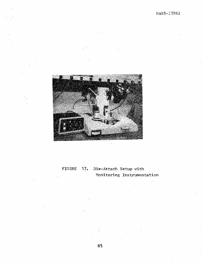
Chip Bonding & Monitorin6
Twenty-four g o l d - s i l i c o n e u t e c t i c bonds were made
with ch ips , preforms and s u b s t r a t e suppl ied by Texas
Ins trument , The thermocompress ion bonding machine used
was t h e K & S Model 642, a l ready shown i n Figure 15, The
bonding opera t ion was monitored with t he Vanzet t i Thermal
T3ond Monitor, Model 1011, a l ready shown i n Figure 13,
The o w r a t i o n a l s e t u p is i l l u s t r a t e d i n Figure 57,
Only one threshold was used, set a t 0a3v peak t o
peak, as read on a Tektronik 535 osc i l loscope , and
ind ica ted by the green threshold l i g h t . A l l bonds t h a t
gave r a d i a t i o n l e v e l s above 0,3v w e r e c l a s s i f i e d as Good,
zlnd all. bonds t h a t were below 0 . 3 ~ w e r e c l a s s i f i e d Poor,
For si-mpliei ty purposes, only t h e r a d i a t i o n l e v e l s of t h e
poor bonds were recorded i n t h e i r numerical magnitude,
td-aile all bonds exceeding, t h e 0 . 3 ~ threshold were j u s t
r-ecorded as .3+. Three of t h e poor bonds w e r e very c lose
t:o 0 , 3 v , These were Nos. 8 , 1- 5 and 21. Unit 81 6 was
ePassified border l ine good because it d id t r i g g e r t h e
th rzshold l e v e l of 0 . 3 ~ ~ but took longer than t h e o t h e r
good bonds t o develop. The following is a t a b u l a t i o n of
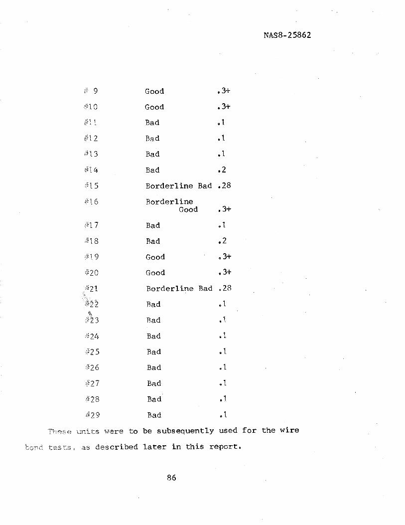
t h e bonds and of t h e Thermal Monitor indica t ionsr
4; 1 Good . 3+
62 Good a 3+
a3 Good .3+
# 4 Good - One corner n o t bonded.
$5 Good a 3+
41 6 Good . 3+
! , 7 Bad .2
/ , 8 Border- l i n e bad. 28
FIGURE 57. Die-Attach Setup with
Monitoring Instrumentation
:-L 9 Good .3+
84. 0 Good
iLTL 1 Bad
#I 2 Bad
-el 3 Bad
//I 4 Bad
$1 5 Borderl ine Bad .28
J'j? 6 Borderl ine Good .3+
i L 1 7 Bad
8 Rad
$?. 9 Good . 3+
4/20 Good . 3+
-'k 2 1 Borderline Bad .28
2 Bad . I 4
523 Bad , I
324 Bad
4 2 5 Bad
$26 Bad .1
dl27 Bad,
$28 Bad
Jj29 Bad . I These units were t o be subsequently used for t h e w i r e
bond tests, as descr ibed la ter i n t h i s repor t .
The o r i g i n a l plan was t o measure s i m u l t a n e ~ u ~ ~ y
the temperature of the c o l l e t t i p and the temperature of
the s i l i c o n chip i n the a rea of the pad t o which the wire
was t o be bonded. For t h i s purpose two Thermal Bond
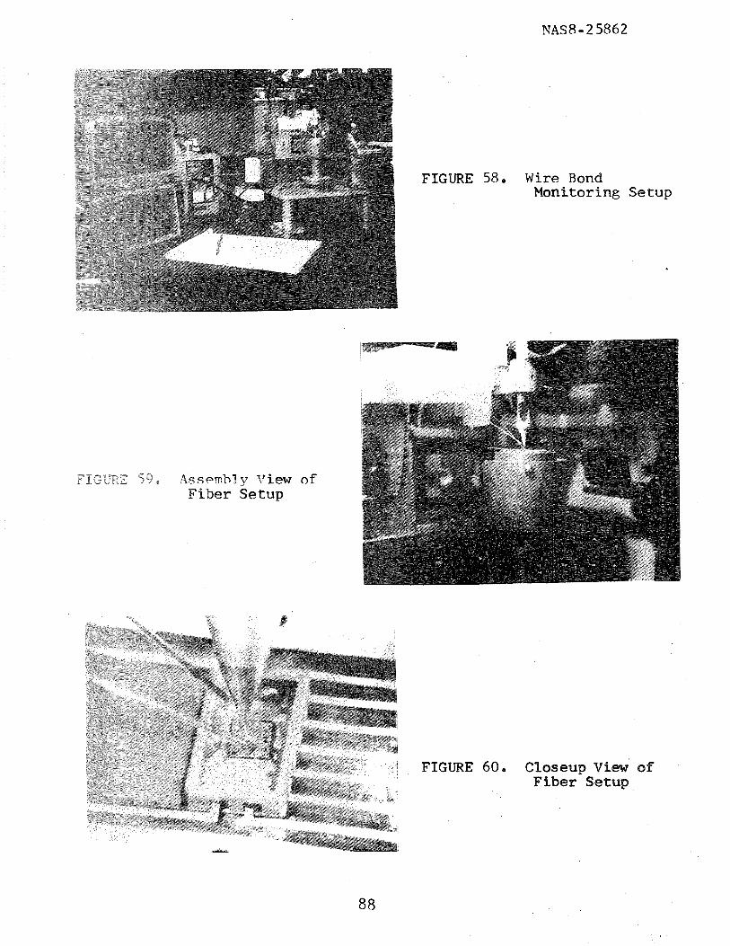
Monitors w e r e needed, and Figure 58 shows t h e i r se tup ,
Figure 59 and Figure 60 show the post t ion of the m o
f i b e r s , of which one points t o the t i p of the bonding
c o l l e t and the o the r points t o t he chip 's pad where the
bond w i l l be located. While the f i r s t one moves up aind
down with the c o l l e t , the second f i b e r t i p is i n a fi.xed
position.
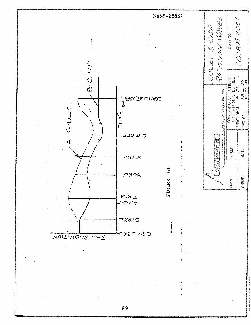
Typical instantaneous rad ia t ion curves of eolle t ( A )
and ehip (B) are shown i n Figure 61. In order to show them
i n t r u e r e l a t i onsh ip , they have been corrected t o compensate
f o r the d i f f e r e n t emiss ivi ty coe f f i c i en t s of the surfaces
being monitored. Our i n t e rp re t a t i on of these curves i s as
follows s
Pr io r t o the beginning of the operat ton, t he semi-
conductor chip ' s temperature is a t a s teady l e v e l ,
somewhat below the e o l l e t " temperature, The eol le t
is a l s o a t s teady temperature.
A s t he c o l l e t moves towards t h e eh ip , i ts highly
r e f l e c t i v e sur face w i l l r e f l e c t more and more of the
c h i p ' s r a d i a t i o n i n t o t h e d e t e c t o r ' s f field of view,
as shown i n t h e ascending por t ion of curve A.
Ar t h e same t i m e , t h e f i e l d of view of f i b e r R is
being cut by t h e c o l l e t ' s t i p , so t h a t r a d i a t i o n
from the ch ip i n t o f i b e r B shows a reduction. This
r e s u l t s i n t h e descending por t ion of t h e beginning
of curve B.
A t the time of contac t between c o l l e t and chip , h e a t
t r a n s f e r hetween those two elements shows up as a
cooling of t h e c o l l e t and a hea t ing of t h e chip.
This is r e f l e c t e d i n t h e r e l a t e d curves,
A s t he contac t is terminated, both the c o l l e t and
the ch ip tend t o resume t h e i r o r i g i n a l temperature,
but the s t i t c h opera t ion brings both curves a t a
lower r a d i a t i o n l e v e l , probably r e l a t e d t o the physical
c h a r a c t e r i s t i c s of t h e l o c a t i o n of the s t i t c h .
F ina l ly , a f t e r c u t o f f , t he curves show an i n i t i a l t r end
totaards t h e i r s teady r a d i a t i o n l e v e l s . These l e v e l s
should bet f o r the c a l l e t , t h e same as before t h e bond;
f o r the chip , a lower l e v e l due t o t h e low emiss iv i ty
f a c t o r of t h e gold bond t h a t now occupies the c e n t e r
of the d e t e c t o r ' s f i e l d of view.
However, repeat ing t h i s procedure r e s u l t e d i n widespread
c h i p radiation measurements because of f i b e r movement, which
changed the r a t i o between meta l l ized and non-metallized a reas
i n the f i e l d of viev~ of the detector . The conclusion
was t h a t it would be necessary t o build a spec i a l f%'ber-
holding f i x t u r e i f w e wanted t o achieve consis tencp re-
peatable measurements. I t w a s decided t h a t , before eqag ing
i n such a complex e f f o r t , w e should t r y t o monitor the
e o l l e t t i p rad ia t ion because,during the cycle , the chip
temperature appears r e f l ec t ed i n the t r a n s i e n t t l p t e m -
perature, s i nce both elements a r e i n int imate physical
contact during the bonding operat inn,
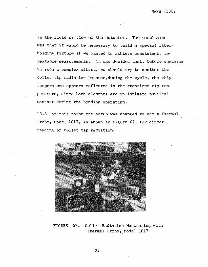
2 0 , 3 A t t h i s point the se tup was changed t o use a %kaermal
Probe, Model 101 7 , as shown i n Figure 6 2 p f o r d i r e c t
reading of c o l l e t t i p radia t ion.
FIGURE 62. Col le t Radiation Monitorfng whth Thermal Probe, Model. 1017
The prel iminary readings taken on t h e Thermal Probe
were not c o n s i s t e n t . Again, it was found t h a t t h e f i b e r
was moving very s l i g h t l y , t he reby occas iona l ly i nc lud ing
some of t h e background i n t h e f i e l d of view, It w a s then
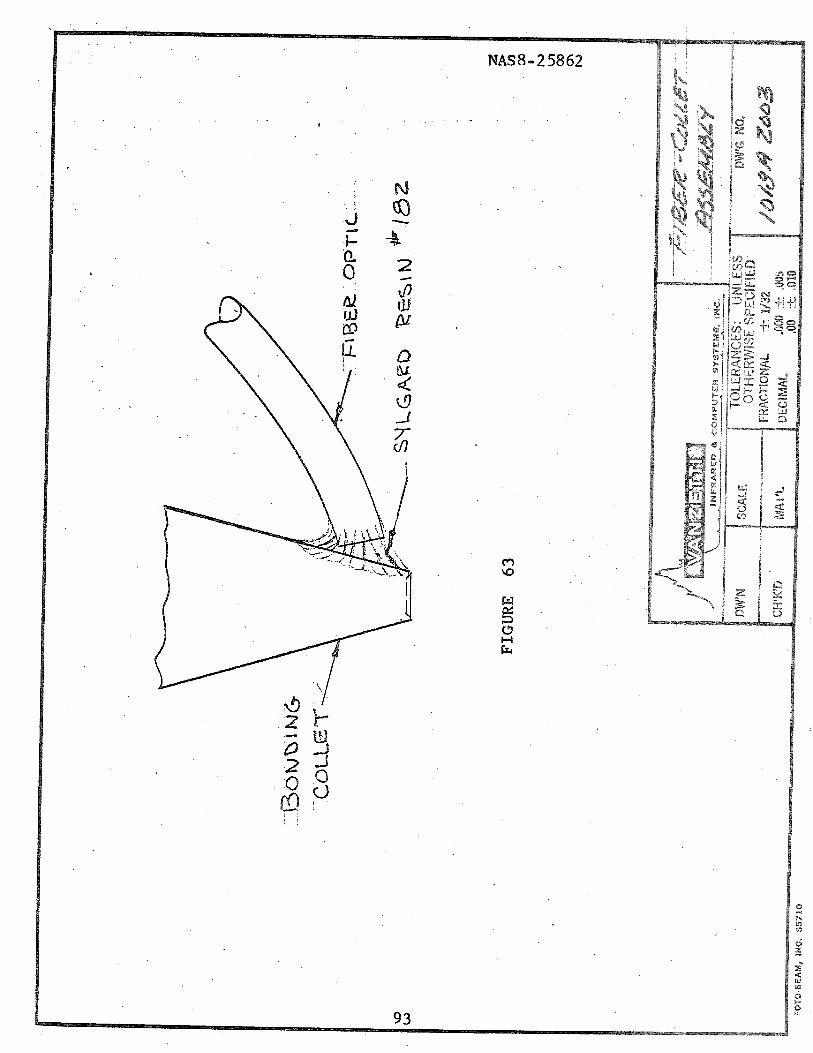
decided t o use Sylgard r e s i n between t h e t i p of t h e
c o l l e t ( s i d e ) and t h e f i b e r (See sketch i n Figure 63) t o
e l iminate background r a d i a t i o n e f f e c t s , The read ings
now were cons is t e n t and r epea t ab l e ,
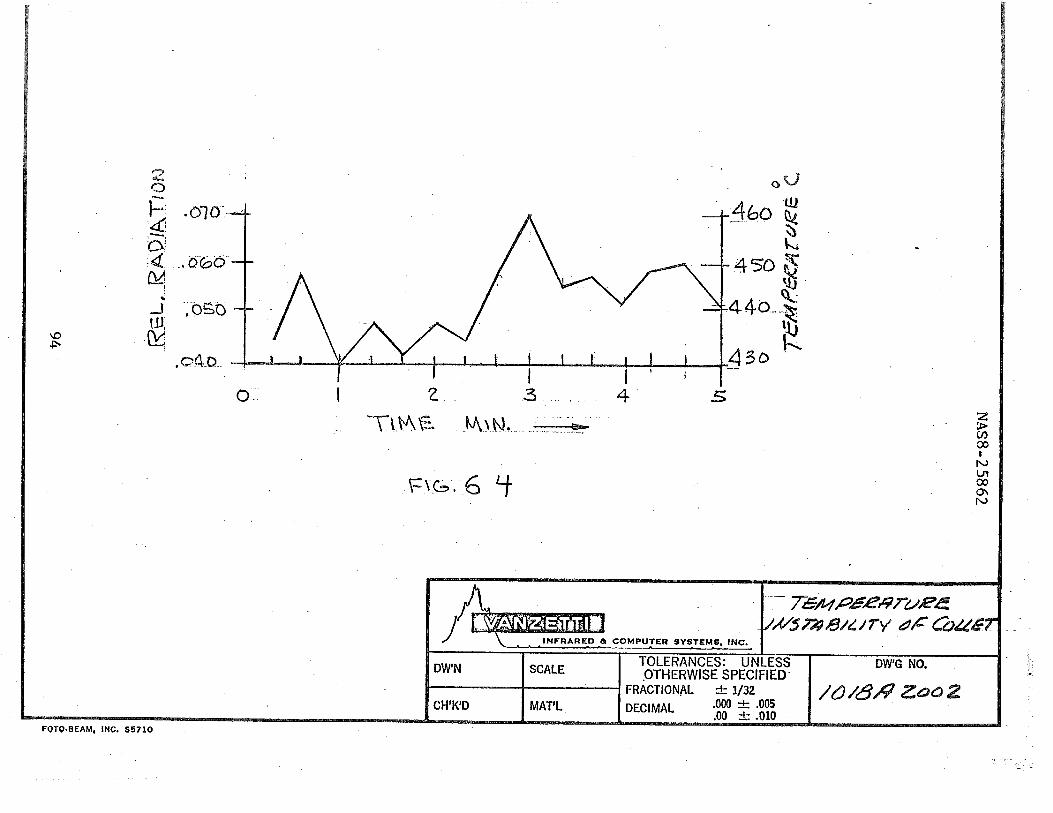
f'leasurements taken t o e v a l u a t e t h e thermal s t a b i l i t y
of the c o l l e t showed wide v a r i a t i o n s , F igure 64 shows
one of t h e many c o r r e l a t i o n curves betb~een r a d i a t i o n ,
temperature , ar,d t i m e d t l r i . ~ g a f l v e minute per iod, A
3 0 " ~ maximum excurs ion i n temperature of t h e t i p of t h e
e o l l e t i s c l e a r l y d e t e c t a b l e . This could be caused by
the cyc l ing of t h e h e a t t a b l e and by convect ion c u r r e n t s
t h a t can coo l t h e t i p d r a s t i c a l l y , I t was no t i ced t h a t
just breathing i n proximity of t h e c o l l e t assembly w a s
causing s e v e r a l degrees of coo l ing i n i t s temperature ,
? 0,3.! T e s t s w e r e run t o determine t h e a p p r o p r i a t e Variac
s e t t i n g s f o r t h e e o f l e t h e a t e r , With t h e Var iac set a t 95%,
tho e o l l e t t i p temperature was 4 3 0 ~ ~ ; w i th t h e Var iac se t 0
a t 70%, t h e co l l . e t t i p temperature w a s 260 C. A t t h e 2 6 0 ' ~
s e t t i n g , w e found w e could th read t h e .0007" gold w i r e
through t h e c o l l e t ho l e . A t t h e h ighe r s e t t i n g of 430°c,
it w a s impossible f o r us t o thread t h e w i r e through the
c o l l e t hole . Even wi th t h e lower s e t t i n g of 2 6 0 ' ~ ~ the
w i r e was c o n s i s t e n t l y pushed back i n t o t h e c o l l e t due
t o t h e bonding pressure on t h e gold b a l l 8 thereby blockin8
t h e hole . The w i r e would then have t o be pul led outo A
tungsten w i r e w a s used t o c l ean t h e h o l e every t i m e it
became plugged. The gold w i r e could then be threaded
through the hole with a g r e a t degree of d i f f i c u l t y , The
w i r e was cont inuously breaking and blocking t h e eo l l e t ,
so t h a t w e w e r e unable t o run a s t a t i s t i c a l l y v a l i d num-
ber of s i g n i f i c a n t tests . Measurements w e r e made of t h e temperature of the
c o l l e t t i p , f i r s t w i th t h e Thermal Probe and immediately
t h e r e a f t e r with a thermocouple appl ied as per t h e instrue-.
t i o n s of t h e Texas Instrument manual, The r e s u l t s were
Thermal Probe - A t a Variac s e t t i n g of 95% 4 3 0 ' ~ $90"~
A t a Variac s e t t i n g of 70% 2 6 0 ' ~ 280"~
These readings mean t h a t t h e thermocouple a c t s as a heat
s i n k and cannot be used t o r e l i a b l y measure t h e t i p
temperature,
2 0 . 3 , 2 On t h e chips #25 through #29, w i r e bonds were
attempted, In every case w e had d i f f i c u l t y wi th the w i r e
breaking and clogging t h e c o l l e t , On u n i t # 2 6 , fourteen
bonds w e r e made, and a l l w e r e acceptable t o a pu l l test
that broke t h e wire before t h e bond f a i l e d . The r a d i a t i o n
measured a t t h e t i p of t h e c o l l e t with the Thermal Probe
f o r each bond was wi th in 5 ' ~ of t h e optimum temperature.
"$&is was accomplished by making a w i r e bond when t h e
mermal Probe indicated t h a t t h e c o l l e t had reached t h e
optimum temperature. The corresponding reading on t h e
mermal Probe was .85 v o l t s , which ind ica tes a c o l l e t
tip temperature of 260°C, due t o the presence of t h e
Sylgard r e s i n , which a c t s not only as a bonding agen t ,
but also as a emiss iv i ty equa l i ze r , s o t h a t the d e t e c t o r
can read blackbody rad ia t ion .
i 0 ,3 ,3 Temperature measurements were made on t h e h o t
galare $0 determine i t s thermal s t a b i l i t y . I t baas found
that i n a s t eady-s ta t e condi t ion the h o t p l a t e cycled
+ 5 " ~ - from t h e set point . The temperature of t h e ho t
plate a t the cen te r measured 5 0 ' ~ higher with the Thermal
Probe, than t h e thermocouple c o n t r o l l e r b u i l t i n t o t h e
h o t plate. Also a g rad ien t of approximately 60°c w a s
found between the cen te r and t h e edge of t h e hot p la te .
% i : 3 again poin ts t o t h e inadequate prec is ion of t h e
thermocouple readings.
10.4 Resul ts of Bonding Tes t s
The r e s u l t s of t h e c h i p bonding tests w e r e t h t
optimum temperature of bond can be adequately determined
with t h e use of a Thermal Bond Monitor Model 101 1 The
r e s u l t s of t h e w i r e bond tests w e r e t h a t t h e c r i t i c a l
parameter, t h e e o l l e t t i p temperature , can be monitored,
s o t h a t it appears poss ib le t o e s t a b l i s h r a d i a t i o n stan-
dards t h a t are i n d i c a t i v e of good q u a l i t y w i r e bonds,
A s i n i t i a l l y planned, work was expended i n t h e following
areas I
Thermal evalua t ion of I C s of t h e type used i n LSI u n i t s ;
R e m a 1 evalua t ion of wafer-subs t r a t e bond qua1 i t y ;
Corre la t ing current flow through semiconductor
junctions with t h e emitted recombination r a d i a t i o n ;
bionitoring t h e a u a l i t y of w i r e bonds during the
bonding opera t ion i t s e l f .
The r e s u l t s , i n syn thes i s , a r e as follows t
" - e F l e e t r i c a l l y opera t ing I C s and LSIs do have t y p i c a l
in f ra red p r o f i l e s . Anomalies t h a t produce va r i a t ions of
the e l e c t r i c a l power d i s s ipa ted by t h e device a r e r e f l e c t e d
i n VaPiations of the in f ra red p r o f i l e . However, d i sp lay i r~g
these var ia t ions i n a way t h a t co~ l ld be eas4ly in te rp re ted
and rou t ine ly processed is the major problem. L a t e r a l
heat t r a n s f e r and emiss iv i ty va r i a t ions add f u r t h e r d i f - f i c u l t y to t h i s techniaue. Any type of in f ra red scanning
microscope can be expected t o po-int out major devia t ions
i n power d i s s i p a t i o n , both i n magnitude and locat ion.
However, pinpointing the cause of the dev ia t ion , a t the
component l e v e l , w i l l be r a t h e r the exception than the ru le .
In t h e p a r t i c u l a r a p p l i c a t i o n t o LSI u n i t s , infrared
f a s t scanning should be expected t o work b e s t a t t h e IC
l e v e l and no t below t h a t s i z e .
11.2 q u a l i t y of t h e bond between wafer and s u b s t r a t e can
success fu l ly be assessed with thermal mapping, Minimum
s i z e of d e t e c t a b l e d e f e c t is dependent on t h e s p a t i a l
r e s o l u t i o n of t h e scanner. The high thermal conduct iv i ty
of s i l i c o n tends t o degrade t h e r e so lu t ion . With an
instantaneous s p o t - s i z e of .02OW, t h e minimum d e t e c t a b l e
de fec t is approximately ,080" i n diameter.
11.3 The e x i s t e n c e of a c o r r e l a t i o n between c u r r e n t flow
through a d i s c r e t e junct ion and t h e recombinat ion radiation
e n i t t e d by it was v e r i f i e d . For LSI u n i t s t h i s means the
c a p a b i l i t y t o monitor, without physical con tac t and i n
r e a l t i m e , t h e flow of e l e c t r i c a l s i g n a l s through the
d i f f e r e n t junct ions of I C s incorporated i n t h e LSI devices,
idhen these s i g n a l s are r e p e t i t i v e pulses , they can be
read n o t on ly i n amplitude, bu t a l s o i n waveshape, by
using t h e Waveform Eduetor t o process t h e ou tpu t of the
Semiconductor Junct ion Analyzer.
1 . 4 Wire bond q u a l i t y appears dependent on t h e tem-
pera tu re condi t ion of t h e t i p of t h e bonding c o l l e t , mis
temperature can be monitored i n real t i m e w i th t h e a"Fsesmal
Probe, A new technique, capable of preventing the fo r -
mation of poor q u a l i t y w i r e bonds, appears now ava i l ab le .
21,5 S t a t i s t i c a l v e r i f i c a t i o n of a l l t h e above- l i s ted
results must be obtained, before s p e c i f i c a t i o n s and pro-
e ed~~res are es tabl i shed . However, w e f e e l t h a t t h e work
expended i n t h i s program has opened the door f o r sub-
stantial enhancement of t h e r e l i a b i l i t y of LSI c i r c u i t s .
RECOMrnND AT IONS
The work performed under t h i s contract has ve r i f i ed the
existence of good po ten t ia l f o r infrared techniques applicable
t o LSI design and manufacturing f o r higher r e l i a b i l i t y i n the
following areas :
a u a l i t y evaluat ion of the waf er-subs t r a t e bond ;
Non-contact measurement of current flow through semi-
conductor junctions ;
In process control of wire bonding.
It is our recommendation t h a t fu r the r e f f o r t be expended
i n the above-mentioned areas i n order t o obta in s t a t i s t i c a l
ve r i f i ca t i ons of the f indings and t o e s t ab l i sh performance and
resolut ion l i m i t s of the in f ra red techniques. To obta in this,
the fo l lo~ r~ i* th ree programs should be planned:
?. 2 , l LSI Wafer-Subs t r a t e Bond Quality Evaluation
Using an in f ra red scanner with a t l e a s t a resolut ion
of ,02OW",can a s t a t i s t i c a l l y va l id number of L S I wafers
which have been bonded t o t h e i r subs t ra tes with the
inclusion of bond f a u l t s of d i f f e r e n t s i z e , shape, and
locat ion, The elements t o be es tabl ished are the following,
a ) type of thermal energizat ion t o be used
b) thermal gradient t o be applied between substrate
and wafer
c ) area resolut ion of the f a u l t s
d) t i m e const ra in ts of the infrared process, s ince
l a t e r a l heat t r ans fe r w i l l tend t o reduce the
area resolut ion a s t i m e goes by.
Tlae infrared scanner bes t sui ted f o r t h i s work is
the INSPECT System, not only because of i t s presently
available fea tures , but a l s o because it was designed . t o
accept a l a s e r f o r instantaneous and local ized thermal
energizaeion of the t a rge t , This approach is explained
in Appendix A and it might embody the optimum solut ion t o
the problem of infrared bond qua l i ty evaluation.
12,2 Current Flow Measurements Throu~h Semiconductor Junctions
Yow t ha t the f e a s i b i l i t y of measuring the current flow
throwh junctions incorporated i n LSI c i r c u i t s has been
demonstrated, a s t a t i s t i c a l l y val id program should be carr ied
o u t $0 es tab l i sh the workable l i m i t s of the process, I n
par t i cu la r , the Semiconductor Junction Analyzer should be
used with d i f f e r en t s i z e f i be r s i n order t o determine f o r
each size junction the area resolut ion t h a t is necessary.
Furthermore, the addit ion of a Waveform Eductor t ha t can
be programmed d i r e c t l y i n to the Semiconductor Junction
k a l y z e r would provide the invest igator with the capa-
bility of observing i n i t s t rue shape the waveform of the
pulses crossing the junction under observation. Elemerhts
t o be invest igated during the recommended program are the
following :
a) minimum s igna l detectable and i t s co r r e l a t i on
t o the size of the junction through which it
flows
b) optimum f i b e r s i z e f o r maximum s igna l resolut ion
c) p o s s i b i l i t y of evaluat ing uniform working
behavior of junctions along the e n t i r e length
and of detect ing points of cur ren t crowding and
cur ren t voids. This should be achieved w i t h the
use of f i b e r s whose diameter is smaller than the
whole area of the junction so t h a t only partf-al
junction areas can be observed one a t a time,
12.3 Wire Bonding Process Control
Ver i f i ca t ion of t he p o s s i b i l i t y of monitoring the
q u a l i t y of the w i r e bonds through c o l l e t thermal measure-
ment should be ca r r ied ou t on a s t a t i s t i c a l l y val id numaber
of w i r e bonds. The plan should cons i s t of recording on
char t the temperature of the c o l l e t t i p a s measured by a
Thermal Bond Monitor instrument; a f t e r t h i s has been done,
pul l tests of the w i r e s should be ca r r i ed out and their
s t rength should be cor re la ted with t he data recorded on
the char t . In t h i s way upper and lower control l i m i t s of
103
the c s lPe t t i p could be es t ab l i shed , so t h a t they could
be applied through a Thermal Bond llonitor instrument f o r
the purpose of process cont ro l of wire bonding.
12,4 The above-mentioned th ree programs, a t t h e i r suc-
cessful eonclusfon, should prove of g r e a t value f o r LSI
rekiahi l i t y enhancement, e s p e c i a l l y i n the following a reas r
a) ::afer to s u b s t r a t e bond q u a l i t y evalua t ion; t h i s
is s t r i c t l y an a f t e r - the - fac t q u a l i t y assessment
operation. I t w i l l be usefu l t o process con t ro l
engineers and t o q u a l i t y cont ro l people. I t w i l l
enhance the r e l i a b i l i t y of LSI u n i t s , due t o the
f a c t t h a t it w i l l enable q u a l i t y cont ro l people
t o e l iminate heat ing of those pa r t s of LSI u n i t s
t h a t a r e loca ted above a bond d e f e c t , where
the necessary hea t s inking is missing.
b) LSI design w i l l he enhanced because the design
engineer w i l l he ab le t o fol lotr , both i n magnitude
and waveform, t h e s i g n a l s a s they t r a v e l through
the 1,SI c i r c u i t r y . g u a l i t y con t ro l engineers
w i l l be a b l e t o make s u r e t h a t production u n i t s
meet t h e performance c h a r a c t e r i s t i c s of t h e
engineering sample. The c a p a b i l i t y of spo t t ing
poin ts of cu r ren t crowding and cur ren t voids
w i l l a l so contr ibute t o reduce the f a i l u r e rate
of LSI un i t s .
c) Real t i m e w i r e bond monitoring w i l l enable
manufacturing people t o keep the process under
con t ro l and avoid making defect ive w i r e bonds,
This again w i l l r e s u l t i n a lower f a i l u r e r a t i o
and higher r e l i a b i l i t y .
12,5 An adequate number of LSI un i t s t h a t have been tested
with the above-mentioned infrared techniques should then
be processed through conventional environmental testing Ln
order t o assess i n r e a l numbers the r e l i a b i l i t y ewancement
so obtained.
Proposal f o r
A FEASIBILITY STUDY
of
A SCANNING HEAT INJECTION SYSTEM
COIJPLED -JITFI A SCAYNING INFRARED DETECTION SYSTEM
PRQPRIETASY IWTICE: This proposal contains p ropr ie t a ry information of Vanzet t i I n f r a r e d & Computer Sys terns, Ine, , and n e i t h e r t h e proposal nor s a i d p ropr ie t a ry information s h a l l be published, reproduced, copied, d i sc losed , or used f o r any purpose o t h e r than cons idera t ion of t h i s proposalB without t h e express , w r i t t e n persmission of a duly author- ized rep resen ta t ive of s a i d Company.
A FEASIBILITY STWY
of
A SCAWZNG 2-:EAT INJECTION SYSTEM
Xnfrared evaluation s f physical ta@;ets f o r material in t eg r i ty , bonding, and other cha rac te r i s t i e s requires thermal ta rge t energization pr ior t o the inf rzlsed masmeem mnt , nree methods a re current ly used t o achieve ~ e r m l . carget energizationr
1, Heat Flood
2, EIeat Soak
3 , Heat "r"rnsfer
In all ehree methods tsfie biggest d i f f i c u l t y is posed by the l a t e ra lmigra t ionof the heat energizing the t a g e t , Tkis eandition grea t ly reduces s p a t i a l resolut ion, often masking indicat ions of anoml ies t h a t coneequsntly remin undetee ted,
NOVEL IC%$PROA@W
A navel approach f o r thermal t a rge t energization has presently becam possible, due t o the a v a i l a b i l i t y of l a se r s of various typesr it could be ca l l ed pulsed point heating, such poSnt being e i t h e r stationaky or moving along a pre-established t r a j ec to ry on the t a r g e t ' s s w f a c e , mis approach eliminates the d i f f i c u l t y dzae t o l a t e r a l heat mfgrat t lo~ by reduein8 t o a small point &e enrea *ere heat i s injected a t every pulse. An infrared r a d i o m t e r focused ow C h i s p s in t w i l l m n i t o r the speed a t whFch the injected heat i s being d l f fused , in to the s u r r o d S n g area. C o m c i n g t h i s information with the "expectedN chaaraeteristle ~ l B allow detect ion of pkBysieal anoml ies of the m t e r i a l a t or n e a $.kae ps in t of beat in jec t ion ,
Use or diselosuge of proposal data i s subject t o the r e s t r i c t i o n on the T i t l e Page of t h i s proposal,
Feas ib i l i ty Study Scanning H e a t
In jec t ion System
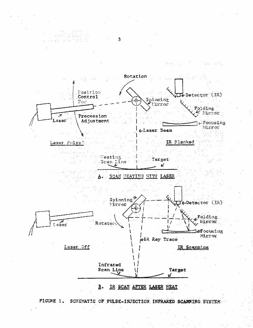
O w company has jus t completed building a scanning Lnnfraaed radionaeter designed i n such a way a s t o allow the addi t ion of a laser fo r instantaneous, localized thermal ensrgization of the target . The l a se r beam is pulsed during the blanking of the detector t o avoid wlwanted s ignal pick up by the l a t t e r , and i s guided by the scanning elements of the optical system, along the same l inear path t h a t w i l l be scarmed by the infrared detector a f rac t ion of a second later, me system w i l l scan the t a rge t e i t h e r ~ t h a single, s t a t i o n e y l i n e , or with a f u l l r a s t e r pattern. The operation i s schelglatieally i l l u s t r a t e d i n Figure 1, I n _A the l a se r is shorn f i r i n g a burst of energy during tha t portion of the opixlning mjirrorb ro t a t i on tha t r e f l e c t s the heating pulse onto a scan l i n e of the t a rge t ; during t h i s period of t i m e the infrared detector i s blanked out , s ince i ts f i e l d of view is physically cu t by the in terposi t ion of the back side of the spinning mirror, After approximately a 90° rotation of the mirror, the detector is shown i n 2 a s scan- ning the same l i n e on the t a rge t while the laser is turned o f f , Variation of the precession in te rva l between heat Lnjection and infrared scanning i s made easy by the posi t ion adjust control t ha t i s p a r t i a l l y shown i n the i l l u s t r a t i on .
The major var iables of t h i s system a re the following, and a e i r optimization should be the goal of the f e a s i b i l i t y study proposed herein:
1, wave length and power of l a se r radia t ion
2 , l a se r pulse duration
3, speed of scan
4, precession of in jec t ion vs. detect ion
5, s i ze of heat ing spot
6 , emissivity of t a rge t surface
Use or disclosure of proposal data is subject t o the resrriction on the Title Tags of this proposal,
Rotation
-, Laser .cdtslse -' I
I
Laser Off
B XR SCAN mEW ..Ie - - -
FIGURE 1, SCNEMATIG OF PaSE-INJECTION IN D SCmmG SYSmiFfZ
Feasibility Study Scanning Heat Injection System
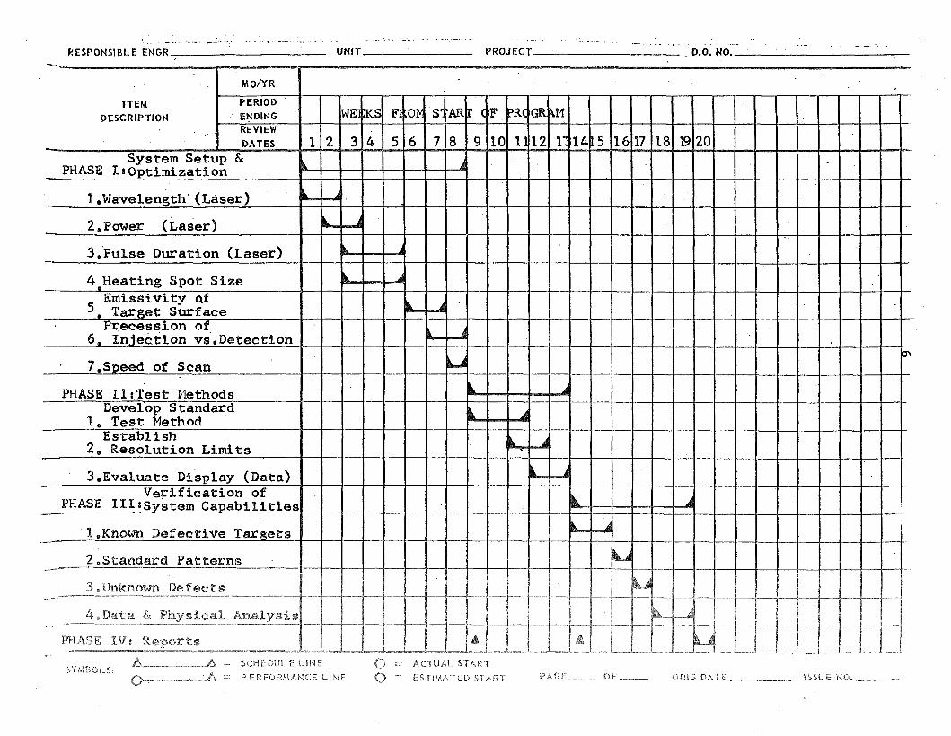
me feasibility study will be carried out in three phases t
Phase I will be devoted to system setup and optimization, ed trade-offs between the six variables listed above
shall be tried in practical operation, using targets con- taining know defects of various size, shape, and location, Cost of system component parts needed for this phase shall not be charged to the program, but cost of targets and of misceXlansous hardware and supplies will be charged to it,
shall be devoted to develop standard target test and evaluation methods that will assure consistency of measurements and repeatability of the infrared profiles, The resolution limits will be established for some of the baed.c defect configurations and dimensions, Comparative evaluation of the different displays available to the system wf ll conclude the effort of this phase of work,
Phase IZI will be the verification of the system capabilities, Targets with defects known only to the customer will be scanned, and the resulting infrared patterns will be corn- pared with the standard patterns of similar units not affected by defects, The deviations will point out Location, size, and shape of the defects, In case of discrepancy, physical analysis shall be carried out in order to find out the reason for it,
Test targets shall include, but not be limited to, panels w % t h bonded sheets, honeycomb assemblies, and multi- layer printed boards,
Use or disclosure of proposal data is subject to the restriction on the Title Page of this proposal,
Feasfbility Study Scanning Heat Injection Sysmem
Interim, informal reports shall be written at the end of each phase. They will sunmarize the work performed, the findings mat-Te, and will doeuroent the rationale for s t a r t i n g work of the next phase.
A Final Report shall be written at the cconclla~fcsm o f the program, Feasibility of the pulsed point heating approech shall be substantiated with the data obtaf ned in the course of the prograln, Specifications for infreed test systens having such a capability will be provided, Test ~ez~sodology will be described in detail and fore- seeable applicatioi?~ of the technique listed along with the predictable limitations.
CFTLOW - After the completion of the program, the customer will
have first priority to purchase the infrared system used to carry out tile feasibility study at a cost that will not exceed rhe price at which the same systems will be sold on the co~imercial market.