Nobel Lecture: Semiconducting and metallic polymers: The fourthgeneration of polymeric materials*
Alan J. Heeger
Department of Physics, Materials Department, Institute for Polymers and Organic Solids,University of California, Santa Barbara, Santa Barbara, California 93106
(Published 20 September 2001)
I. INTRODUCTION
In 1976, Alan MacDiarmid, Hideki Shirakawa, and I,together with a talented group of graduate students andpostdoctoral researchers, discovered conducting poly-mers and the ability to dope these polymers over the fullrange from insulator to metal (Chiang et al., 1977;Shirakawa et al., 1977). This was particularly exciting be-cause it created a new field of research on the boundarybetween chemistry and condensed-matter physics, andbecause it created a number of opportunities:
• Conducting polymers opened the way to progress inunderstanding the fundamental chemistry and physics ofp-bonded macromolecules;
• Conducting polymers provided an opportunity toaddress questions that had been of fundamental interestto quantum chemistry for decades:
Is there bond alternation in long-chain polyenes?What is the relative importance of the electron-
elecron and the electron-lattice interactions in p-bondedmacromolecules?
• Conducting polymers provided an opportunity toaddress fundamental issues of importance to condensed-matter physics as well, including, for example, the metal-insulator transition as envisioned by Neville Mott andPhilip Anderson and the instability of one-dimensionalmetals discovered by Rudolph Peierls (the ‘‘Peierls In-stability’’).
• Finally—and perhaps most important—conductingpolymers offered the promise of achieving a new gen-eration of polymers: Materials which exhibit the electri-cal and optical properties of metals or semiconductorsand which retain the attractive mechanical propertiesand processing advantages of polymers.Thus, when asked to explain the importance of the dis-covery of conducting polymers, I offer two basic an-swers:
(i) They did not (could not?) exist.(ii) They offer a unique combination of properties not
available from any other known materials.
The first expresses an intellectual challenge; the secondexpresses a promise for utiltity in a wide variety of ap-plications.
*The 2000 Nobel Prize in Chemistry was shared by Alan J.Heeger, Alan G. MacDiarmid, and Hideki Shirakawa. This lec-ture is the text of Professor Heeger’s address on the occasionof the award.
0034-6861/2001/73(3)/681(20)/$24.00 681
Conducting polymers are the most recent generationof polymers (Ranby, 1993). Polymeric materials in theform of wood, bone, skin, and fibers have been used byman since prehistoric time. Although organic chemistryas a science dates back to the eighteenth century, poly-mer science on a molecular basis is a development of thetwentieth century. Hermann Staudinger developed theconcept of macromolecules during the 1920s.Staudinger’s proposal was openly opposed by leadingscientists, but the data eventually confirmed the exis-tence of macromolecules. Staudinger was awarded theNobel Prize in Chemistry in 1953 ‘‘for his discoveries inthe field of macromolecular chemistry.’’ While carryingout basic research on polymerization reactions at theDuPont Company, Wallace Carothers invented nylon in1935. Carothers’s research showed the great industrialpotential of synthetic polymers, a potential that becamereality in a remarkably short time. Today, synthetic poly-mers are used in larger quantities than any other class ofmaterials (larger by volume and larger by weight, eventhough such polymers have densities close to unity).Polymer synthesis in the 1950s was dominated by KarlZiegler and Giulio Natta, whose discoveries of polymer-ization catalysts were of great importance for the devel-opment of the modern ‘‘plastics’’ industry. Ziegler andNatta were awarded the Nobel Prize in Chemistry in1963 ‘‘for their discoveries in the field of the chemistryand technology of high polymers.’’ Paul Flory was thenext ‘‘giant’’ of polymer chemistry; he created modernpolymer science through his experimental and theoreti-cal studies of macromolecules. His insights and deep un-derstanding of macromolecular phenomena are summa-rized in his book, Principles of Polymer Chemistry,published in 1953 and still useful (and used) today. Florywas awarded the Nobel Prize in Chemistry in 1974 ‘‘forhis fundamental achievements, both theoretical and ex-perimental, in the physical chemistry of macromol-ecules.’’
Because the saturated polymers studied byStaudinger, Flory, Ziegler, and Natta are insulators, theywere viewed as uninteresting from the point of view ofelectronic materials. Although this is true for saturatedpolymers (in which all of the four valence electrons ofcarbon are used up in covalent bonds), in conjugatedpolymers the electronic configuration is fundamentallydifferent. In conjugated polymers, the chemical bondingleads to one unpaired electron (the p electron) per car-bon atom. Moreover, p bonding, in which the carbonorbitals are in the sp2pz configuration and in which the
682 Alan J. Heeger: Semiconducting and metallic polymers
FIG. 1. Molecular structures of examples ofconjugated polymers. Note the bond-alternated structures.
orbitals of successive carbon atoms along the backboneoverlap, leads to electron delocalization along the back-bone of the polymer. This electronic delocalization pro-vides the ‘‘highway’’ for charge mobility along the back-bone of the polymer chain.
As a result, therefore, the electronic structure in con-ducting polymers is determined by the chain symmetry(i.e., the number and kind of atoms within the repeatunit), with the result that such polymers can exhibitsemiconducting or even metallic properties. In his lec-ture at the Nobel Symposium (NS-81) in 1991, ProfessorBengt Ranby designated electrically conducting poly-mers as the ‘‘fourth generation of polymeric materials’’(Ranby, 1993).
The classic example is polyacetylene, (2CH)n , inwhich each carbon is s bonded to only two neighboringcarbons and one hydrogen atom with one p electron oneach carbon. If the carbon-carbon bond lengths wereequal, the chemical formula, (2CH)n with one unpairedelectron per formula unit, would imply a metallic state.Alternatively, if the electron-electron interactions weretoo strong, (2CH)n would be an antiferromagnetic Mottinsulator. The easy conversion to the metallic state on
Rev. Mod. Phys., Vol. 73, No. 3, July 2001
doping (Chiang et al., 1977; Shirakawa et al., 1977) to-gether with a variety of studies of the neutral polymerhave eliminated the antiferromagnetic Mott insulator asa possibility.
In real polyacetylene, the structure is dimerized as aresult of the Peierls instability with two carbon atoms inthe repeat unit, (2CHvCH)n . Thus the p band is di-vided into p and p* bands. Since each band can holdtwo electrons per atom (spin up and spin down), the pband is filled and the p* band is empty. The energydifference between the highest occupied state in the pband and the lowest unoccupied state in the p* band isthe p-p* energy gap Eg . The bond-alternated structureof polyacetylene is characteristic of conjugated polymers(see Fig. 1). Consequently, since there are no partiallyfilled bands, conjugated polymers are typically semicon-ductors. Because Eg depends upon the molecular struc-ture of the repeat unit, synthetic chemists are providedwith the opportunity and the challenge to control theenergy gap by design at the molecular level.
Although initially built upon the foundations of quan-tum chemistry and condensed-matter physics, it soon be-came clear that entirely new concepts were involved in
683Alan J. Heeger: Semiconducting and metallic polymers
the science of conducting polymers. The discovery ofnonlinear excitations in this class of polymers, solitons insystems in which the ground state is degenerate and con-fined soliton pairs (polarons and bipolarons) in systemsin which the ground-state degeneracy has been lifted bythe molecular structure, opened entirely new directionsfor the study of the interconnection of chemical andelectronic structure. The spin-charge separation charac-teristic of solitons and the reversal of the spin-chargerelationship (relative to that expected for electrons asfermions) in polyacetylene challenged the foundationsof quantum physics. The study of solitons in polyacety-lene (Heeger et al., 1988), stimulated by the Su-Schrieffer-Heeger (SSH) papers (Su et al., 1979, 1980),dominated the first half of the 1980s.
The opportunity to synthesize new conducting poly-mers with improved/desired properties began to attractthe attention of synthetic chemists in the 1980s. Al-though it would be an overstatement to claim that chem-ists can now control the energy gap of semiconductingpolymers through molecular design, we certainly havecome a long way toward that goal.
Reversible ‘‘doping’’ of conducting polymers, with as-sociated control of the electrical conductivity over thefull range from insulator to metal, can be accomplishedeither by chemical doping or by electrochemical doping.Concurrent with the doping, the electrochemical poten-tial (the Fermi level) is moved either by a redox reactionor an acid-base reaction into a region of energy wherethere is a high density of electronic states; charge neu-trality is maintained by the introduction of counterions.Metallic polymers are, therefore, salts. The electricalconductivity results from the existence of charge carriers(through doping) and from the ability of those chargecarriers to move along the p-bonded ‘‘highway.’’ Conse-quently, doped conjugated polymers are good conduc-tors for two reasons:
(i) Doping introduces carriers into the electronicstructure. Since every repeat unit is a potentialredox site, conjugated polymers can be doped ntype (reduced) or p type (oxidized) to a relativelyhigh density of charge carriers (Chiang et al.,1978).
(ii) The attraction of an electron in one repeat unit tothe nuclei in the neighboring units leads to carrierdelocalization along the polymer chain and tocharge-carrier mobility, which is extended intothree dimensions through interchain electrontransfer.
Disorder, however, limits the carrier mobility and, in themetallic state, limits the electrical conductivity. Indeed,research directed toward conjugated polymers with im-proved structural order and hence higher mobility is afocus of current activity in the field.
Figure 2 shows the early results on the conductivity ofpolyacetylene as a function of the doping level; even inthese early studies the conductivity increased by morethan a factor of 107 to a level approaching that of ametal (Chiang et al., 1977).
Rev. Mod. Phys., Vol. 73, No. 3, July 2001
The electrochemical doping of conducting polymerswas discovered by the MacDiarmid-Heeger collabora-tion in 1980 and opened the way to research in yet an-other scientific direction (Nigrey et al., 1979). The elec-trochemistry of conducting polymers has developed intoa field of its own with applications that range from poly-mer batteries and electrochromic windows to light-emitting electrochemical cells (Pei et al., 1995).
Although I have emphasized the processing advan-tages of polymers, even as late as 1990 there were noknown examples of stable metallic polymers which couldbe processed in the metallic form (a requirement forbroad use in industrial products). This major outstand-ing problem was first solved with polyaniline, PANI.PANI has been investigated extensively for over 100years and attracted interest as a conducting material forseveral important reasons: the monomer is inexpensive,the polymerization reaction is straightforward and pro-ceeds with high yield, and PANI has excellent stability.As shown by Alan MacDiarmid and his collaborators inthe mid 1980s, polyaniline can be rendered conductingthrough two independent routes, oxidation (eitherchemically or electrochemically) of the leuco-emeraldine base or protonation of the emeraldine basethrough acid-base chemistry (Salaneck et al., 1986). Be-cause the insertion of counterions is involved in bothroutes, conducting polyaniline is a salt (a polycation withone anion per repeat unit).
Processing high-molecular-weight polyaniline intouseful objects and devices proved to be a difficult prob-
FIG. 2. Electrical conductivity of trans-(CH), as a function of(AsF5) dopant concentration. The trans and cis polymer struc-tures are shown in the inset.
684 Alan J. Heeger: Semiconducting and metallic polymers
lem. Yong Cao, Paul Smith, and I made importantprogress in 1991 by using functionalized protonic acidsto both convert PANI to the metallic form and, simulta-neously, render the resulting PANI complex soluble incommon organic solvents (Cao et al., 1992). The func-tionalized counterion acts like a ‘‘surfactant’’ in that thecharged head group is ionically bound to the oppositelycharged protonated PANI chain, and the ‘‘tail’’ is chosento be compatible with nonpolar or weakly polar organicliquids (in the case of solutions) or the host polymer (inthe case of blends). The processibility of PANI inducedby the ‘‘surfactant’’ counterions has made possible thefabrication of conducting polymer blends with a varietyof host polymers (Cao et al., U.S. patent 5,232,631).Since the blends are melt-processible as well, thecounterion-induced processibility of polyaniline pro-vides a route to conducting polymer blends for use inindustrial products. The ‘‘surfactant’’ counterions offeran unexpected advantage: they lead to the formation ofa self-assembled network morphology in the PANIpolyblends (Yang et al., 1992). Because of these inter-penetrating networks, the threshold for the onset ofelectrical conductivity in blends with traditional insulat-ing host polymers is reduced to volume fractions wellbelow 1% (Reghu et al., 1993). The PANI network issufficiently robust that it remains connected and con-ducting even after the removal of the host polymer, thusopening the way to research in another new direction,the fabrication of novel electrodes for use in electronicdevices. The use of ‘‘surfactant’’ counterions was intro-duced with the goal of making PANI processible in theconducting form. The self-assembly of phase-separatednetworks was an unexpected—but very welcome—bonus.
Conducting polymers were initially attractive becauseof the fundamental interest in the doping and thedoping-induced metal-insulator transition. However, thechemistry and physics of these polymers in their non-doped semiconducting state are of great interest becausethey provide a route to ‘‘plastic electronic’’ devices. Al-though polymer diodes were fabricated and character-ized in the 1980s, (Tomazawa et al., 1987, 1989), the dis-covery of light-emitting diodes (LED’s) by RichardFriend and colleagues at Cambridge in 1990 (Bur-roughes et al., 1990) provided the stimulus for a majorpush in this direction. The polymer light-emitting diodeis, however, only one of a larger class of devices in theemerging class of ‘‘plastic’’ optoelectronic devices, in-cluding lasers, high-sensitivity plastic photodiodes (andphotodiode arrays) and photovoltaic cells, ultrafast im-age processors (optical computers), thin-film transistors,and all-polymer integrated circuits; in each case thesesophisticated electronic components are fabricated fromsemiconducting and metallic polymers. All of these havea common structure: They are thin-film devices in whichthe active layers are fabricated by casting the semicon-ducting and/or metallic polymers from solution (e.g.,spin casting or ink-jet printing).
Rev. Mod. Phys., Vol. 73, No. 3, July 2001
II. DOPING
Charge injection onto conjugated, semiconductingmacromolecular chains, ‘‘doping,’’ leads to the wide va-riety of interesting and important phenomena which de-fine the field. As summarized in Fig. 3, reversible chargeinjection by ‘‘doping’’ can be accomplished in a numberof ways.
A. Chemical doping by change transfer
The initial discovery of the ability to dope conjugatedpolymers involved charge-transfer redox chemistry: oxi-dation (p-type doping) or reduction (n-type doping),(Chiang et al., 1977, 1978; Shirakawa et al., 1977), as il-lustrated with the following examples:
(a) p type
~p-polymer!n1 32 ny~I2!→@~p-polymer!1y~I3
2!y#n ;(1)
(b) n type
~p-polymer!n1@Na1~Napthtalide!* #y
→@~Na1!y~p-polymer!2y#n1~Naphth!0. (2)
When the doping level is sufficiently high, the electronicstructure evolves to that of a metal.
B. Electrochemical doping
Although chemical (charge-transfer) doping is an effi-cient and straightforward process, it is typically difficultto control. Complete doping to the highest concentra-tions yields reasonably high quality materials. However,attempts to obtain intermediate doping levels often re-sult in inhomogeneous doping. Electrochemical dopingwas invented to solve this problem (Nigrey et al., 1979).In electrochemical doping, the electrode supplies the re-dox charge to the conducting polymer, while ions diffuseinto (or out of) the polymer structure from the nearbyelectrolyte to compensate the electronic charge. Thedoping level is determined by the voltage between theconducting polymer and the counterelectrode; at elec-trochemical equilibrium the doping level is precisely de-
FIG. 3. Doping mechanisms and related applications.
685Alan J. Heeger: Semiconducting and metallic polymers
fined by that voltage. Thus doping at any level can beachieved by setting the electrochemical cell at a fixedapplied voltage and simply waiting as long as necessaryfor the system to come to electrochemical equilibrium(as indicated by the current through the cell going tozero). Electrochemical doping is illustrated by the fol-lowing examples:
(a) p type
~p-polymer!n1@Li1~BF42!#sol’n
→@~p-polymer!1y~BF12!y#n1Li~electrode!;
(3)
(b) n type
~p-polymer!n1Li~electrode!
→@~Li1!y~p-polymer!2y#n1@Li1~BF42!#sol’n .
(4)
C. Doping of polyaniline by acid-base chemistry
Polyaniline provides the prototypical example of achemically distinct doping mechanism (Salaneck et al.,1986). Protonation by acid-base chemistry leads to aninternal redox reaction and the conversion from semi-conductor (the emeraldine base) to metal (the emeral-dine salt). The doping mechanism is shown schemati-cally in Fig. 4. The chemical structure of thesemiconducting emeraldine base form of polyaniline isthat of an alternating copolymer. Upon protonation ofthe emeraldine base to the emeraldine salt, the proton-induced spin unpairing mechanism leads to a structuralchange with one unpaired spin per repeat unit, but withno change in the number of electrons (Wudl et al., 1987;
FIG. 4. Protonation-induced spin unpairing in polyaniline;conversion from insulator to metal with no change in the num-ber of electrons.
Rev. Mod. Phys., Vol. 73, No. 3, July 2001
MacDiarmid and Epstein, 1990). The result is a half-filled band and, potentially, a metallic state in whichthere is a positive charge in each repeat unit (from pro-tonation) and an associated counterion (e.g., Cl2,HSO4
2 , DBSA2, etc.: the counterion is not shown inFig. 4). This remarkable conversion from semiconductorto metal has been well described, but it is not well un-derstood from the view of basic theory. There are nocalculations that show that the metallic (emeraldine salt)final state is lower in energy than the semiconductor andno detailed understanding of the rearrangement reac-tions sketched in Fig. 4.
D. Photodoping
The semiconducting polymer is locally oxidized and(nearby) reduced by photoabsorption and charge sepa-ration (electron-hole pair creation and separation into‘‘free’’ carriers):
~p-polymer!n1hn→@$p-polymer%1y
1$p-polymer%2y#n , (5)
where y is the number of electron-hole pairs (dependentupon the pump rate in competition with the recombina-tion rate). The branching ratio between free carriers andbound excitons (and the closely related issue of the mag-nitude of the exciton binding energy) is a subject of con-tinuing discussion (Sariciftci, 1998).
Following photoexcitation from the ground state (1Agin the notation of molecular spectroscopy) to the lowest-energy state with proper symmetry (1Bu), one finds thatrecombination to the ground state can be either radia-tive (luminescence) or nonradiative. Some families ofconjugated polymers exhibit high-luminescence quan-tum efficiencies (for example, PPV and PPP and theirsoluble derivatives); others do not (for example, poly-acetylene and the polythiophenes). A number of mecha-nisms have been identified that lead to low quantumefficiencies for photoluminescence. Rapid bond relax-ation in the excited state and the formation of solitonswith states at midgap prevent radiative recombination inpolyacetylene (Heeger et al., 1988). The existence of anAg state or a triplet excited state below the 1Bu statewill favor nonradiative recombination (in both cases, di-rect radiative transitions to the ground state are forbid-den). Interchain interactions in the excited state (‘‘exci-mers’’) also lead to nonradiative channels for decay(Jenekhe and Osaheni, 1994; Rothberg et al., 1996; Cor-nil et al., 1998).
E. Charge injection at a metal-semiconducting polymer(MS) interface
Electrons and holes can be injected from metallic con-tacts into the p* and p bands, respectively:
(a) Hole injection into an otherwise filled p band
@~p-polymer!n2y~e2!→~p-polymer!1y# ; (6a)
(b) Electron injection into an empty p* band
686 Alan J. Heeger: Semiconducting and metallic polymers
@~p-polymer!n1y~e2!→~p-polymer!2y#n . (6b)
In the case of charge injection at an MS interface, thepolymer is oxidized or reduced (electrons are added tothe p* band or removed from the p band). However, thepolymer is not doped in the sense of chemical or elec-trochemical doping, for there are no counterions. Thisdistinction becomes particularly clear when comparingcharge injection in the polymer light-emitting diode(where there are no ions; Burroughes et al., 1990;Parker, 1994) with that in the polymer light-emittingelectrochemical cell, where electrochemical doping withassociated redistribution of ions provides the mechanismfor charge injection (Nigrey et al., 1979).
As indicated in Fig. 3, each of the methods of charge-injection doping leads to unique and important phenom-ena. In the case of chemical and/or electrochemical dop-ing, the induced electrical conductivity is permanent,until the carriers are chemically compensated or untilthe carriers are purposely removed by ‘‘undoping.’’ Inthe case of photoexcitation, the photoconductivity istransient and lasts only until the excitations are eithertrapped or decay back to the ground state. In the case ofcharge injection at a metal-semiconductor interface,electrons reside in the p* band and/or holes reside in thep band only as long as the biasing voltage is applied.
Because of the self-localization associated with theformation of solitons, polarons, and bipolarons, chargeinjection leads to the formation of localized structuraldistortions and electronic states in the energy gap (Hee-ger et al., 1988). In the case of ‘‘photodoping,’’ the redis-tribution of oscillator strength associated with subgapinfrared absorption and the corresponding bleaching ofthe interband (p-p*) transition provide a route to non-linear optical (NLO) response. Real occupation of low-energy excited states (Heeger et al., 1988; Maniloff et al.,1997) and virtual occupation of higher-energy excitedstates (in the context of perturbation theory; Chianget al., 1992) lead to, respectively, resonant and nonreso-nant NLO response.
By charge-injection doping at an MS interface, onecan use the polymer semiconductor as the active ele-ment in thin-film diodes (Tomozawa et al., 1987, 1989)and field-effect transistors (FET’s) (Burroughes et al.,1988; Garnier et al., 1994; Drury et al., 1998). Tomozawaet al. (1987, 1989) demonstrated the first example of anelectronic device component fabricated by casting theactive polymer directly from solution; even these earlydiodes exhibited excellent current-voltage characteris-tics. Dual carrier injection in metal/polymer/metal struc-tures provides the basis for polymer light-emitting di-odes (Parker, 1994). In polymer LED’s, electrons andholes are injected from the cathode and anode, respec-tively, into the undoped semiconducting polymer; light isemitted when the injected electrons and holes meet inthe bulk of the polymer and recombine with the emis-sion of radiation (Burroughes et al., 1990).
Thus, as summarized in Fig. 3, doping is a commonfeature of conducting polymers; doping leads to a re-markably wide range of electronic phenomena.
Rev. Mod. Phys., Vol. 73, No. 3, July 2001
III. NOVEL PROPERTIES GENERATE NEW TECHNOLOGY
As emphasized in the Introduction, conducting poly-mers exhibit novel properties not typically available inother materials. I focus on a few of these as illustrativeexamples:
(a) Semiconducting and metallic polymers that aresoluble in and processible from common solvents;
(b) Transparent conductors;(c) Semiconductors in which the Fermi energy can be
controlled and shifted over a relatively wide range.
In each case, the property is related to a fundamentalfeature of the chemistry and/or physics of the class ofconducting polymers. These novel properties make pos-sible a number of applications including polymer LED’s,conducting polymers as electrochromic materials, poly-mer photodetectors, and polymer photovoltaic cells.
A. Semiconducting and metallic polymers that are solublein and processible from common solvents
Because the interchain electron transfer interactionsof conjugated polymers are relatively strong comparedwith the van der Waals and hydrogen bonding interchaininteractions typical of saturated polymers, conductingpolymers tend to be insoluble and infusible. Thus therewas serious doubt in the early years following the dis-covery that p-conjugated polymers could be doped tothe metallic state as to whether or not processing meth-ods could be developed. Significant progress has beenmade using four basic approaches:
(1) Side-chain functionalization, principally used forprocessing semiconducting polymers from solutionin organic solvents or from water;
(2) Precursor route chemistry, principally used for pro-cessing polyacetylene and poly(phenylene vinylene)(PPV) into thin films;
(3) Counterion-induced processing, principally used forprocessing polyaniline in the metallic form from or-ganic solvents;
(4) Aqueous colloidal dispersions created by templatesynthesis, principally used for processing polyanilineand poly(ethylenedioxythiophene), PEDOT.
The addition of moderately long side chains onto themonomer units resulted in derivatives of polythiophene,the poly(3-alkylthiophenes), or P3AT’s, see Fig. 1. Sincethe side chains decrease the interchain coupling and in-crease the entropy, these derivatives can be processedeither from solution or from the melt. Similarly, side-chain functionalization of poly(phenylene vinylene),PPV (see Fig. 1), has progressed to the point where avariety of semiconducting polymers and copolymers areavailable with energy gaps that span the visible spectrum(Hide et al., 1996). Water solubility was achieved by in-corporating polar groups such as (CH2)nSO3
2M1 intothe side chains (so-called ‘‘self-doped’’ polymers; Koba-yashi et al., 1985; Heeger and Smith, 1991).
687Alan J. Heeger: Semiconducting and metallic polymers
The ability to fabricate optical-quality thin films byspin casting from solution has proven to be an enablingstep in the development of plastic electronic devicessuch as diodes, photodiodes, LED’s, light-emitting elec-trochemical cells (LEC’s), optocouplers, and thin-filmtransistors (Yu and Heeger, 1996).
The counterion-induced processibility of ‘‘metallic’’polyaniline utilizes bifunctional counterions such asdodecylbenzenesulfonate to render the polymer soluble(Cao, Smith, and Heeger, 1992). The charge on the SO3
2
head group forms an ionic bond with the positive charge(proton) on the PANI chain; the hydrocarbon tail‘‘likes’’ organic solvents. Processing PANI in the con-ducting form resulted in materials with improved homo-geneity and crystallinity, and with correspondingly im-proved electrical conductivities (Menon et al., 1998).The solubility of ‘‘metallic’’ PANI in organic solvents hasalso made possible the fabrication of conducting blendsof PANI with a variety of insulating host polymers (Cao,Smith, and Heeger, 1992, patent). These polymer blendsexhibit a remarkably low percolation threshold as a re-sult of the spontaneous formation of an interpenetratingnetwork morphology (Yang et al., 1992).
Template-guided synthesis of conducting polymerswas first reported by S. C. Yang and colleagues (Hey-wang and Jonas, 1992; Sun and Yang, 1992). The mo-lecular template, in most cases polyacids such as polysty-rene sulfonic acid, binds the monomer, for exampleaniline, to form molecular complexes that are dispersedin water as colloidal particles. Upon polymerization, theaniline monomers form polyaniline and remain attachedto the template to form the template-polyaniline com-plex. By judicious choice of the template molecule andthe polymerization conditions, stable submicron-sizecolloidal particles of polyaniline-template aggregate canbe formed during polymerization. The stabilizationagainst coagulation arises from the Coulomb repulsionbetween particles, which is a result of the surface chargeprovided by the extra sulfonic acid groups in polystyrenesulfonic acid. Very stable dispersions of polyaniline-polystyrene sulfonic acid complexes can be made withparticle sizes less than 1 mm (Heywang and Jonas, 1992;Sun and Yang, 1992). Transparent films with a specificresistivity of 1–10 V cm can be cast from such disper-sions.
Poly(ethylenedioxythiophene)-polystyrene sulfonate(PEDOT-PSS) can be prepared as a stable dispersion inwater (Heywang and Jonas, 1992; Sun and Yang, 1992;Friedrich and Werner, U.S. patent 5,300,575). Films ofPEDOT-PSS are semitransparent and can be spin castwith a surface resistance of approximately 500 V/squareand with 75% transmission.
B. Transparent metallic polymers
Metals reflect light at frequencies below the plasmafrequency vp , defined as
vp254pNe2/m* , (7)
Rev. Mod. Phys., Vol. 73, No. 3, July 2001
where N is the number of electrons per unit volume, e isthe electron charge, and m* is the effective mass (the‘‘optical mass’’) of the electrons in the solid. At frequen-cies above the plasma frequency, metals are transparent(Kittel, 1986). For conventional metals (Na, Cu, Ag,etc.), N is of order 1023 per unit volume. As a result, theplasma frequency is in the ultraviolet; therefore conven-tional metals appear shiny and ‘‘metallic looking’’ in thespectral range over which the human eye is sensitive.
Metallic polymers have a lower density of electrons;both the length of the repeat unit along the chain andthe interchain spacing are relatively large compared tothe interatomic distances in conventional metals. Typi-cally therefore for metallic polymers N is of order 2–531021 cm23. Thus, for metallic polymers, the plasma fre-quency is at approximately 1 eV (Lee, Heeger, and Cao,1993; Lee et al., 1995). The reflectance of high quality,metallic polypyrrole (doped with PF6) is shown in Fig. 5.Metallic polymers exhibit high reflectance (and thuslook ‘‘shiny’’) in the infrared, but they are semitranspar-ent in the visible part of the spectrum. The residual ab-sorption above the plasma frequency arises from inter-band (p-p* ) transitions between the partially filled pband and the lowest-energy p* band.
Optical-quality thin films of metallic polymers are use-ful, therefore, as transparent electrodes (Cao, Treacy,et al., 1992). For example, polyaniline (Gustafsson et al.,1992), polypyrrole (Gao et al., 1996), and PEDOT (Caoet al., 1997) have been used as transparent hole-injectingelectrodes in polymer LED’s (the initial demonstrationof mechanically flexible polymer LED’s utilized PANI asthe anode (Gustafsson et al., 1992). Transparent con-ducting films can be used for a variety of purposes; forexample, as antistatic coatings, as electrodes in liquid-crystal display cells or in polymer LED’s, or for fabricat-ing electrochromic windows.
C. Semiconductors in which the Fermi energy can beshifted across the energy gap
In comparison with traditional inorganic semiconduc-tors, semiconducting polymers cannot be considered ma-
FIG. 5. Reflectance spectra of PPy-PF6 near the metal-insulator transition; the inset shows the low-energy spectrawith expanded scale.
688 Alan J. Heeger: Semiconducting and metallic polymers
terials with ultrahigh purity. As a result, although manydevice concepts have been demonstrated using semicon-ducting polymers as the active materials (Yu and Hee-ger, 1996), there was early skepticism that these novelsemiconductors could be used in commercial applica-tions.
In some ways, however, semiconducting polymers aremore robust than their inorganic counterparts. In par-ticular, whereas pinning of the Fermi energy by surfacestates is a major problem in conventional semiconduc-tors, the Fermi energy can be controlled and shifted allthe way across the energy gap in conjugated polymers.The absence of Fermi-level pinning and the ability toshift the chemical potential all the way across the energygap are fundamentally important; these novel featuresof semiconducting polymers underlie the operation ofpolymer LED’s, polymer LEC’s, and polymer photo-diodes.
One might have expected chemical reactions betweenthe metal electrode and the polymer to lead to interfacestates that pin the Fermi level, as in inorganic semicon-ductors. Experiments have shown, however, that theseinterfacial interactions do not lead to pinning of theFermi level. For example, electroabsorption measure-ments were used to determine the built-in electric fieldin metal-semiconductor-metal (MSM) structures of thekind used for polymer LED’s (Campbell et al., 1996).The results indicated that the maximum internal field isnearly equal to the single-particle energy gap; thebuilt-in field directly tracked the difference in workfunctions of the two metal electrodes, as originally pro-posed by Parker (1994). Thus the Fermi level is notpinned by surface states. The absence of Fermi-levelpinning in semiconducting polymers is a major advan-tage: Conceptually, it greatly simplifies the device phys-ics, and technologically, it greatly simplifies the devicefabrication.
IV. SEMICONDUCTING POLYMERS: ELECTRONICSTRUCTURE AND BOND RELAXATION IN EXCITEDSTATES
A. Band structure, electron-lattice interaction, electron-electron interaction, and disorder
Although the linear and nonlinear optical propertiesof conducting polymers have been investigated for overa decade, there is still controversy over the descriptionof the elementary excitations. Are the lowest-energy el-ementary excitations mobile charge carriers (chargedpolarons) either injected at the contacts or created di-rectly via interband photoexcitation, or are the lowest-energy excitations bound neutral excitons (Sariciftci,1998)? The answer is of obvious importance from theperspective of our basic understanding of the physics ofconducting polymers. The answer is also important forapplications based on these materials.
The central issue relates to the strength of theelectron-electron interactions relative to the bandwidth,relative to the electron-phonon interaction, and relative
Rev. Mod. Phys., Vol. 73, No. 3, July 2001
to the strength of the mean disorder potential. Strongelectron-electron interactions (electron-hole attraction)lead to the creation of localized and strongly correlatednegative and positive polaron pairs: neutral polaron ex-citons. Well-screened electrons and holes with associ-ated lattice distortions (charged polarons), on the otherhand, are more appropriately described using a bandpicture supplemented by the electron-phonon interac-tion. Molecular solids such as anthracene (Pope andSwenberg, 1982) are examples of the former, where theabsorption is dominated by excitonic features, whereasinorganic semiconductors such as Si and GaAs are ex-amples of the latter, where rigid band theory is a goodapproximation.
The electronic structure of conjugated polymers wasdescribed by Su, Schrieffer, and Heeger (1979, 1980) interms of a quasi-one-dimensional tight-binding model inwhich the p electrons are coupled to distortions in thepolymer backbone by the electron-phonon interaction.In the SSH model, photoexcitation across the p-p*band gap creates the self-localized, nonlinear excitationsof conducting polymers: solitons (in degenerate ground-state systems), polarons, and bipolarons (Heeger et al.,1988). Direct photogeneration of solitons and polaronsis made possible by the Franck-Condon overlap betweenthe uniform chain in the ground state and the distortedchain in the excited state (Hagler et al., 1991; Hagler andHeeger, 1992). When the ground state is nondegenerate,as in the PPV’s, charged polaron pairs can either sepa-rate as mobile charged polarons or form bound polaronexcitons, i.e., neutral bipolarons bound by a combinationof their Coulomb attraction and their shared distortion.Photoluminescence can be described in terms of the ra-diative decay of polaron excitons.
Conjugated polymers are p-bonded macromolecules,molecules in which the fundamental monomer unit isrepeated many, many times. Thus N, the Staudinger in-dex as in (CH)N , is large. Since the end points are notimportant when N is large, the p-electron transfer inte-gral [denoted as ‘‘b’’ in molecular orbital theory (Streit-weiser, 1961) and ‘‘t’’ in tight-binding theory] tends todelocalize the electronic wave functions over the entiremacromolecular chain. This tendency toward delocaliza-tion is limited by disorder (which tends to localize thewave functions) and by the Coulomb interaction, whichbinds electrons when transferred to a nearby repeat unitto the positive charge left behind i.e., to the ‘‘hole.’’
In principle, disorder can be controlled. Chain-extended and chain-aligned samples can be prepared.Indeed, by utilizing the method of gel processing ofblends of conjugated polymers in polyethylene (Smithet al., 1981), a high degree of structural order has beenattained (Hagler et al., 1991; Hagler and Heeger, 1992).Thus, as a starting point, it is useful to consider idealizedsamples in which the macromolecular chains are chainextended and chain aligned.
The relative importance of the Coulomb interactionversus the band structure is a classic problem of thefield. In tight-binding theory, the p-electron band struc-ture extends over a bandwidth, W52zt, where z is the
689Alan J. Heeger: Semiconducting and metallic polymers
number of nearest neighbors. Thus, for linear polymerswith z52 and t'2.5 eV, W'10 eV (Heeger et al., 1988).Since the size of the monomer, typically 5–10 Å alongthe chain axis, is the smallest length in the problem, themonomer length is the effective ‘‘Bohr radius.’’ Thus, ongeneral grounds, one expects the electron-hole bindingenergy to be reduced from 13.5 eV (the electron-protonCoulomb binding energy in the H atom, where the Bohrradius is 0.53 Å) by a factor of 10–20 simply because ofthe change in length scale. Dielectric screening providesan additional reduction factor of «, where «'3 (typicalof conjugated polymers) is the dielectric constant for anelectric field along the chain. Thus the binding energy isexpected to be no more than a few tenths of an eV. Sincethe typical bandwidths and band gaps are all in the eVrange, one can start with a one-electron band approachand treat the Coulomb energy as a perturbation. In thisdescription, the electron-hole bound states are Wannierexcitons which are delocalized over a number of repeatunits. There are obvious cases where this argumentbreaks down. For example, one finds that in structurescontaining benzene rings, specific subbands have band-widths near zero (nodes in the wave function reduce theeffective transfer integral to zero). When electrons andholes occupy such narrow bands, the corresponding ex-citons are easily localized by the Coulomb interactiononto a single monomer. Thus, in general, one can expectboth ‘‘Wannier-like’’ excitons and ‘‘Frenkel-like’’ exci-tons for electrons and holes originating from differentbands in the same polymer.
B. Electronic structure of polyacetylene
Trans-polyacetylene, trans-(CH)x , was the first highlyconducting organic polymer (Shivakawa et al., 1977;Chiang et al., 1977). The simple molecular structure,uCHu units repeated [see Fig. 6(a)], implies that eachcarbon contributes a single pz electron to the p band. Asa result, the p band would be half filled. Thus, based
FIG. 6. Polyacetylene: (a) undimerized structure; (b) dimer-ized structure due to the Peierls instability; (c) cis-polyacetylene; (d) degenerate A and B phases in trans-polyacetylene; (e) soliton in trans-polyacetylene; (f) structuralrelaxation in vicinity of domain boundary.
Rev. Mod. Phys., Vol. 73, No. 3, July 2001
upon this structure, an individual chain of neutral poly-acetylene would be a metal; since the electrons in thisidealized metal could move only along the chain, poly-acetylene would be a metal; since the electrons in thisidealized metal could move only along the chain, poly-acetylene would be a one-dimensional (1D) metal. How-ever, experimental studies show clearly that neutralpolyacetylene is a semiconductor with an energy gap ofapproximately 1.5 eV. Rudolf Peierls (1955) showedmany years ago that 1D metals are unstable with respectto a structural distortion which opens an energy gap atthe Fermi level, thus rendering them semiconductors. Inthe Peierls instability, the periodicity (L5p/kF) of thedistortion is determined by the magnitude of the Fermiwave vector (kF). Since kF5p/2a for the half-filled bandof trans-(CH)x , the Peierls distortion doubles the unitcell, converting trans-polyacetylene into trans-(uHCvCHu)x ; see Fig. 6(b) where, schematically,the dimerization is drawn as alternating single bondsand double bonds (in reality, shorter and longer bonds).The p band of (CH)x is split into two subbands, a fullyoccupied p band (the valence band in semiconductorterminology) and an empty p* band (the conductionband), each with a wide bandwidth (;5 eV) and signifi-cant dispersion. The resulting band structure and associ-ated density of states, shown in Fig. 7, results from theopening of the band gap that originates from the dou-bling of the unit cell as a result of the bond alternationcaused by the Peierls instability of the 1D metal.
Shortly after the initial discovery of doping and themetal-insulator transition in polyacetylene, the SSH de-scription of the electronic structure was proposed (Suet al., 1979, 1980). The construction of the remarkablysuccessful SSH Hamiltonian was based on two assump-tions: (a) The p-electronic structure can be treated inthe tight-binding approximation with a transfer integralt'2.5 eV, and (b) the chain of carbon atoms is coupled tothe local electron density through the length of thechemical bonds,
tn ,n115t01a~un112un!, (8)
where tn ,n11 is the bond-length-dependent hopping in-tegral from site n to n11, and un is the displacementfrom equilibrium of the nth carbon atom. The first as-sumption defines the lowest-order hopping integral t0 inthe tight-binding term that forms the basis of the Hamil-
FIG. 7. Electronic structure of semiconducting polyacetylene:left, band structure; right, density of states. The energy opensat k5p/2a as a result of the Peierls distortion.
690 Alan J. Heeger: Semiconducting and metallic polymers
tonian. The second assumption provides the first-ordercorrection to the hopping integral. This term couples theelectronic states to the molecular geometry, giving theelectron-phonon interaction where a is the electron-phonon coupling constant. The bond-length-dependenthopping integral is physically correct, as indicated bybond alternation observed in polyacetylene (Fincheret al., 1982; Yannoni and Clarke, 1983). The precise formof Eq. (8), in which the dependence of the hopping in-tegral on the C-C distance is linearized for small devia-tions about t0 , is the first term in a Taylor expansion.The resulting SSH Hamiltonian is then written as thesum of three terms (Su et al., 1979, 1980):
HSSH5(n ,s
@2t01a~un112un!#~cn11,s1 cn ,s1cn ,s
1 cn11,s!
1(n
F pn2
2m1
12
Kn~un112un!2G , (9)
where pn are the nuclear momenta, un are the displace-ments from equilibrium, m is the carbon mass, and K isan effective spring constant. The cn ,s
1 and cn ,s are thefermion creation and annihilation operators for site nand spin s. The last two terms are, respectively, a har-monic ‘‘spring constant’’ term which represents the in-crease in potential energy that results from displacementfrom the uniform bond lengths in (CH)x and a kinetic-energy term for the nuclear motion.
The spontaneous symmetry breaking that results fromthe Peierls instability implies that for the ground state ofa pristine chain, the total energy is minimized foruunu.0. Thus, to describe the bond alternation in theground state,
un→^un&5~21 !nu0 . (10)
With this mean-field approximation, the value u0 whichminimizes the energy of the system can be calculated asa function of the other parameters in the Hamiltonian(Su et al., 1979, 1980; Heeger et al., 1988). Qualitatively,however, one sees that u0 and 2u0 both minimize theenergy for trans-polyacetylene, since the bonds all makethe same angle with respect to the chain axis. Hence theenergy as a function of u has a double minimum at 6u0 ,as shown in Fig. 8. The corresponding structures of thetwo degenerate ground states are shown in Fig. 6(d).The double minimum of Fig. 8 implies that nonlinearexcitations, solitons, will be important. In polymers witha nondegenerate ground state, the degeneracy indicated
FIG. 8. Total energy of the dimerized polyacetylene chain.Note the double minimum associated with the spontaneoussymmetry breaking and the twofold-degenerate ground.
Rev. Mod. Phys., Vol. 73, No. 3, July 2001
in Fig. 8 is lifted; for a nondegenerate ground-state poly-mer, the absolute minimum energy occurs at a singlevalue of u.
C. The electronic structure of poly(phenylene vinylene)
Poly(phenylene vinylene), PPV, and its soluble deriva-tives have emerged as the prototypical luminescentsemiconducting polymers. Since PPV has a nondegener-ate ground state, structural relaxation in the excitedstate leads to the formation of polarons, bipolarons, andneutral excitons. Prior to treating the structural relax-ation in the excited state, however, one needs to developa satisfactory description of the electronic excited states.
In PPV, with eight carbons in the main-chain repeatunit, the p band is split into eight subbands. Since eachband can hold precisely two electrons per repeat unit,the four p subbands with the lowest energy are filledand the four p* subbands are empty. Thus I begin with adescription at the one-electron level, i.e., from the pointof view of band theory.
Brazovskii, Kirova, and Bishop (Brazovskii et al.,1998; Kirova et al., 1999) treated the band structure ofPPV with a tight-binding Hamiltonian, using standardvalues for the hopping integrals. The electron-phononcoupling, Eq. (8), can be included after defining the ba-sic band structure of the semiconductor. From thissimple ansatz, basis states that reflect the intrinsic sym-metry of the phenyl ring and the dimer were calculatedand used to expand the wave function. The basis stateshybridize as a result of ring-to-dimer hopping, thusyielding the 61258 subbands in the p system of PPV.
The resulting band structure, Fig. 9, has a number ofimportant features. Six of the subbands (three occupiedand three unoccupied), labeled D and D* in Fig. 9, arebroad, and the corresponding wave functions are delo-calized along the chain. The other two bands, labeled Land L* (one occupied and one unoccupied), are narrow,and the corresponding wave functions have amplitudesthat are localized on the ring. The L and L* subbandsderive from the two ring states whose wave functionshave nodes at the para linkage sites; as a result, thesestates do not participate in hopping and the subbands donot acquire the resulting dispersion. On the contrary, the
FIG. 9. Electronic band structure of PPV.
691Alan J. Heeger: Semiconducting and metallic polymers
delocalized D and D* subbands have relatively high dis-persion (;1.7 eV), indicating good delocalization overboth ring and dimer states.
Starting from this simple yet physically robust modelof the band structure, the discussion of the electronicstructure can be extended to include the effect of theCoulomb interaction. The delocalized nature of D1 andD1* implies that, for electron correlation effects involv-ing these subbands, it is appropriate to compute an ef-fective mass from the dispersion curves and then com-pute the corresponding one-dimensional (1D)hydrogenic levels. From the k2 dependence of the dis-persion near the zone center, the effective masses in D1and D1* are m* 50.067me .
Using the well-known result for the binding energy ofa hydrogeniclike state in 1D, the exciton associated withthe lowest-energy electronic transition (D1-D1* ) has abinding energy and effective radii given by
Eb5Eb* ln2~ab /a'! ab5ab* @ ln~ab /a'!#21, (11a)
where
Eb* 5m* e4
«2\2 ab* 5\2«
m* e2 , (11b)
« is the dielectric susceptibility, \ is Planck’s constant,m* is the electron effective mass at the zone center in kspace (for PPV, m* ' 0.067me), e is the electron charge,and a''2 Å (the ‘‘width’’ of the chain). From Eq. (11),Eb'0.1–0.2 eV (depending on the value assumed fora') and a radius of approximately 30 Å.
In addition to this weakly bound Wannier-Mott exci-ton, there are two other excitons in this model. The de-generate D1-L1* and L1-D1* transitions are treatedby assuming an immobile (massive) carrier in the L orL* subband and a mobile carrier in the D or D* sub-band. The resulting bound state has a binding energy of;0.8 eV and is a more tightly bound (but still somewhatdelocalized) exciton. Finally, the L-L* transition formsa very tightly bound Frenkel exciton, localized on thephenyl ring.
With the electronic excitations established, they canbe compared to the data obtained from optical absorp-tion measurements. An unambiguous test of the agree-ment between the proposed electronic structure (Fig. 9)and experiment requires data from chain-extended andchain-oriented samples of macromolecular PPV’s. Withmacromolecular samples, chain-end boundary condi-tions are not important; with oriented polymers, the po-larization of the various absorptions with respect to thechain axis can be determined. Recent polarized absorp-tion studies of highy oriented PPV and polyparaphe-nylene (PPP) indicate that the one-electron model is agood starting point (Miller et al., 1999, 2000).
D. Solitons, polarons, and polaron excitons: Theelementary excitations of conducting polymers
Although bond relaxation in the excited state is im-plicitly allowed through the bond-length-dependenthopping integral in the SSH model, the effect of bond
Rev. Mod. Phys., Vol. 73, No. 3, July 2001
relaxation and the formation of solitons, polarons, andbipolarons have not been treated explicitly in the previ-ous section. These important concepts are summarizedin the following paragraphs. In the related experimentalstudies, trans-polyacetylene and polythiophene wereused as the model systems for the degenerate ground-state polymer and the nondegenerate ground-state poly-mer, respectively (Heeger et al., 1988).
1. Solitons
Charge storage on the polymer chain leads to struc-tural relaxation, which in turn localizes the charge. Thesimplest example of the dramatic effect of this structuralrelaxation is the soliton in trans-polyacetylene. The soli-ton is a domain boundary between the two possible de-generate ground-state configurations of trans-(uCHvCHu)N , the ‘‘A’’ phase and the ‘‘B’’ phase.For simplicity, we often draw the chemical structure ofthe soliton as an abrupt change from A phase to Bphase, as shown in Fig. 6(e). In agreement with the pre-dictions of the SSH model (Heeger et al., 1988), how-ever, the experimental evidence indicates that the struc-tural relaxation in the vicinity of the domain boundaryextends over approximately 14 carbon atoms, as illus-trated in Fig. 6(f). The corresponding spin and chargedistributions are similarly delocalized.
The value of a picture like Fig. 6(e) quickly becomesevident when one tries to understand the quantum num-bers of the soliton and the reversed charge-spin relation-ship that characterizes the solitons of polyacetylene [seeFig. 10(c)]. Since the nonbonding, or midgap, stateformed by the chain relaxation can be mapped to a
FIG. 10. Polarons in semiconducting polymers: (a) schematicpicture of a polaron in PPP; (b) band diagram of an electronpolaron; for a hole polaron, the lower gap state is single occu-pied and the upper gap state is empty; (c) band diagrams forpositive and negative solitons with associated electronic tran-sitions.
692 Alan J. Heeger: Semiconducting and metallic polymers
specific atomic site, the resulting distribution of chargeand spin can be easily addressed; if the state is unoccu-pied (doubly occupied), the carbon atom at the bound-ary is left with a positive (negative) charge, but there areno unpaired spins; the charged soliton is positively(negatively) charged and spinless. Single occupation ofthe soliton state neutralizes the electronic charge of thecarbon nucleus, while introducing an unpaired spin ontothe chain. The localized electronic state associated withthe soliton is a nonbonding state at an energy which liesat the middle of the p-p* gap, between the bonding andantibonding levels of the perfect chain. On the otherhand, the defect is both topological and mobile due tothe translational symmetry of the chain. Such a topologi-cal and mobile defect is historically referred to as a soli-ton (Su et al., 1979, 1980; Heeger et al., 1988). The term‘‘soliton’’ (S) refers simultaneously to all three types ofsolitons; the quantum numbers for spin and charge enteronly when referring to a specific type (for example, neu-tral solitons found as defects from the synthesis of un-doped material or charged solitons created by photoex-citation), and even then, the spin is only implicit.Another feature of the soliton terminology is the naturaldefinition of an ‘‘antisoliton’’ (AS) as a reverse bound-ary from B phase back to A phase in Figs. 6(e) and 6(f).The antisoliton allows for conservation of soliton num-ber upon doping or upon photoexcitation.
2. Polarons and bipolarons
In cases such as poly(thiophene), PPV, PPP, and cis-polyacetylene where the two possible bond alternationpatterns are not energetically degenerate, confinedsoliton-antisoliton pairs, polarons, and bipolarons, arethe stable nonlinear excitation and the stable chargestorage states (Brazovskii and Kirova, 1981; Fesser et al.,1983). A polaron can be thought of as a bound state of acharged soliton and a neutral soliton whose midgap en-ergy states hybridize to form bonding and antibondinglevels. The neutral soliton contributes no charge and asingle spin, as noted above, and the charged soliton car-ries a charge of 6e and no spin; the resulting polaronthen has the usual charge-spin relationship of fermions:q56e and s5 1
2. The polaron is illustrated schematicallyfor PPP in Figs. 10(a) and (b). The positive polaron is aradical cation, the negative polaron a radical anion; bothare quasiparticles consisting of a single electronic chargedressed with a local geometrical relaxation of the bondlengths. Similarly, a bipolaron is a bound state of twocharged solitons of like charge (or two polarons whoseneutral solitons annihilate each other) with two corre-sponding midgap levels, as illustrated in Figs. 11(a) and(b). Since each charged soliton carries a single electroniccharge and no spin, the bipolaron has charge 62e andzero spin. The positive bipolaron is a spinless dication,the negative bipolaron a spinless dianion: both are dou-bly charged bound states of two polarons bound to-gether by the overlap of a common lattice distortion orenhanced geometrical relaxation of the bond lengths.
Rev. Mod. Phys., Vol. 73, No. 3, July 2001
3. Solitons and polarons in conjugated polymers:Experimental Results
The models outlined above for solitons, polarons, andbipolarons make concrete predictions of experimentallyobservable phenomena, and indeed theoretical progresswould not have been possible without concurrent ex-perimental investigation. Optical probes of the midgapelectronic states [see Fig. 10(c)] and magnetic measure-ments of spin concentrations and spin distributions con-tributed greatly to the refinement and verification oftheoretical predictions. For a detailed review of the ex-perimental results, the reader is referred to the Reviewsof Modern Physics article on this subject (Heeger et al.,1988).
V. PHOTOINDUCED ELECTRON TRANSFER
The discovery of photoinduced electron transfer incomposites of conducting polymers (as donors, D) andbuckminsterfullerene, C60, and its derivatives (as accep-tors, A) opened a number of new opportunities for semi-conducting polymers (Morita et al., 1992; Sariciftci et al.,1992). A schematic description of the photoinducedelectron transfer process is displayed in Fig. 12.
FIG. 11. Bipolarons in polymer with nondegenerate groundstate: (a) schematic picture of a negative bipolaron in PPP; (b)band diagram for a negative bipolaron. For a positive bipo-laron, both gap states are unoccupied.
FIG. 12. Photoinduced electron transfer from a conjugatedsemiconducting polymer to C60.
693Alan J. Heeger: Semiconducting and metallic polymers
A broad range of studies has been carried out to fullycharacterize this photoinduced charge transfer, culmi-nating with a study of the dynamics of photoinducedelectron transfer from semiconducting polymers to C60using fs time-resolved measurements (Kraabel et al.,1994, 1996, Lanzani et al., 2000). These studies demon-strated that the charge transfer occurs within 50 fs afterphotoexcitation. Since the charge transfer rate is morethan 1000 times faster than any competing process (theluminescence lifetime is greater than 300 ps), the quan-tum efficiency for charge separation approachesUNITY! Moreover, the charge-transferred state is meta-stable (Smilowitz et al., 1993; Sariciftci and Heeger,1994).
Semiconducting polymers are electron donors uponphotoexcitation (electrons promoted to the antibondingp* band). The idea of using this property in conjunctionwith a molecular electron acceptor to achieve long-livedcharge separation is based on the stability of the photo-induced nonlinear excitations (such as polarons) on theconjugated polymer backbone. Buckminsterfullerene,C60, is an excellent electron acceptor capable of takingon as many as six electrons (Allemand et al., 1991). Itforms charge-transfer salts with a variety of strong do-nors. It is reasonable, therefore, to consider electrontransfer from photoexcited semiconducting polymers toC60. Figure 13 shows a schematic energy-level diagramof the photoinduced electron (or hole) transfer process,which can be described in terms of the following steps:
where the donor (D) and acceptor (A) units are eithercovalently bound (intramolecular) or spatially close, butnot covalently bonded (intermolecular); 1 and 3 denotesinglet or triplet excited states, respectively.
Since the partial charge transfer at step 3 is stronglydependent on the surrounding medium, there is a con-tinuous range for the transfer rate, 0,d,1. At step 4,d51, i.e., a whole electron is transferred. At each step,the D-A system can relax back to the ground state ei-ther by releasing energy to the ‘‘lattice’’ (in the form ofheat) or through light emission (provided the radiativetransition is allowed). The electron-transfer step (Step4) describes the formation of an ion radical pair; thisdoes not occur unless ID* 2AA2UC,0, where ID* is theionization potential of the excited state (D* ) of the do-nor, AA is the electron affinity of the acceptor, and UC isthe Coulomb energy of the separated radicals (includingpolarization effects). Stabilization of the charge separa-tion (Step 5) can be achieved by carrier delocalizationon the D1 (and/or A2) species and by structural relax-ation. The symmetrical process of hole transfer from thephotoexcited acceptor to the donor is described in ananalogous way and can be driven by photoabsorption inspectral regions where the acceptor can be photoexcitedbut not the donor.
Even though the photoinduced electron-transfer reac-tion is energetically favorable, energy must be conservedin the process. In semiconducting polymers, the excessenergy is readily taken up by promoting the hole to ahigher energy state in the p* band. Ultimately, there-fore, the ultrafast nature of the photoinduced electron-transfer process results from the delocalized nature ofthe p electrons. Once the photoexcited electron is trans-ferred to an acceptor unit, the resulting cation radical(positive polaron) species on the conjugated polymerbackbone is relatively stable. Thus photoinduced elec-tron transfer from the conjugated polymer donor ontoan acceptor moiety can be viewed as ‘‘photodoping’’ (seeFig. 3). The forward-to-reverse asymmetry of the photo-induced charge separation in the conducting polymer/C60 system is nevertheless remarkable; the asymmetry isorders of magnitude greater than that observed in thephotosynthesis of green plants.
Definitive evidence of charge transfer and chargeseparation was obtained from light-induced electronspin resonance (LESR) experiments (Sariciftci et al.,1992; Lee et al., 1994; Sariciftci and Heeger, 1994). Uponilluminating the conjugated polymer/C60 compositeswith light with hv.Ep-p* , where Ep-p* is the energygap of the conjugated polymer (donor), two photoin-duced electron spin resonance (ESR) signals can be re-solved, one at g52.00 and the other at g51.99 (Sariciftciet al., 1992; Sariciftci and Heeger, 1994). The higherg-value line is assigned to the conjugated polymer cation
694 Alan J. Heeger: Semiconducting and metallic polymers
(polaron) and the lower g-value line to the C602 anion.
The assignment of the lower g-value line to C602 is un-
ambiguous, for this low g value was measured earlier(Allemand et al., 1991); the higher g value is typical ofconjugated polymers. The LESR signal vanishes above200 K; this rules out permanent photochemical changesas the origin of the ESR signal and demonstrates thereversibility of the photoinduced electron transfer. Theintegrated LESR intensity shows two peaks with equiva-lent intensities. The temperature dependence of theLESR signal intensity shows Arrhenius behavior withactivation energy of approximately 15 meV. This resultsuggests a phonon-assisted back relaxation mechanismof the photoinduced charge-separated state (Sariciftciand Heeger, 1994).
In MEH-PPV/C60 composites, the strong photo-luminescence of MEH-PPV (poly[2-methoxy-5-(28-ethyl)hexyloxy-1,4-phenylene vinylene) is quenchedby a factor in excess of 103, and the luminescence decaytime is reduced from t05550 ps to trad!60 ps (the instru-mental resolution), indicating that charge transfer hascut off the radiative decay (Sariciftci et al., 1992; Smilow-itz et al., 1993; Sariciftci and Heeger, 1994). An estimateof the transfer rate, 1/tct , can be obtained from thequenching of the photoluminescence:
1/tct'~1/trad!I0 /Icomp , (12)
where 1/t0 and 1/trad are the radiative decay rates, andI0 and Icomp are the integrated photoluminescence inten-sities of MEH-PPV and the MEH-PPV/C60 composite,respectively. The data imply therefore that 1/tct. 1012; i.e., electron transfer occurs on the subpicosec-ond time scale. The ultrafast charge-transfer process wassubsequently time resolved (Kraabel et al., 1994, 1996;Lanzani et al., 2000); the data directly confirm thatcharge transfer occurs within a hundred femtoseconds.
The photoinduced electron-transfer process serves tosensitize the photoconductivity of the semiconductingpolymer (Lee, Yu, et al., 1993). Time-resolved transientphotocurrent measurements indicate that the addition ofas little as 1% of C60 into the semiconducting polymerresults in an increase of initial photocurrent by an orderof magnitude. This increase of the photocarrier genera-tion efficiency is accompanied by an increase in lifetimeof the photocarriers upon adding C60. Thus the ultrafastphotoinduced electron transfer from the semiconductingpolymer onto C60 not only enhances the charge-carriergeneration in the host polymer but also serves to pre-vent recombination by separating the charges and stabi-lizing the charge separation.
Conjugated polymers with higher electron affinities(e.g., cyano-substituted PPV) function as the acceptorcomponent, with MEH-PPV as the donor (Halls et al.,1995; Yu and Heeger, 1995). Through control of themorphology of the phase separation into an interpen-etrating bicontinuous network of D and A phases, highinterfacial area was achieved within a bulk material: a‘‘bulk D/A heterojunction’’ that yields efficient photoin-duced charge separation (Halls et al., 1995; Yu and Hee-
Rev. Mod. Phys., Vol. 73, No. 3, July 2001
ger, 1995; Yu et al., 1995; Yang and Heeger, 1996). Theseall-polymer phase-separated blends were successfullyused in fabricating solar cells with efficiencies that ap-proach those fabricated from amorphous silicon (Yuet al., 1995).
VI. METALLIC POLYMERS AND THE METAL-INSULATORTRANSITION
A. Metallic polymers with high-performance electrical andmechanical properties
An early (and continuing) goal of the field of conduct-ing polymers was the creation of materials with highelectrical conductivity and with the excellent mechanicalproperties of polymers. This goal has been achieved;more importantly, the conditions for realizing this com-bination of properties are understood and can be ap-plied to new materials.
Electrical conductivity results from the existence ofcharge carriers and the ability of those carriers to move.In principle, broad p-electron bandwidths (often severaleV) can lead to relatively high carrier mobilities (Hee-ger et al., 1988). As a result of the same intrachain pbonding and the relatively strong interchain electron-transfer interaction, the mechanical properties (Young’smodulus and tensile strength) of conjugated polymer arepotentially superior to those of saturated polymers.Thus metallic polymers offer the promise of truly highperformance: high conductivity plus superior mechanicalproperties.
This combination of high electrical conductivity andoutstanding mechanical properties has been demon-strated for doped polyacetylene (Akagi et al., 1989;Tsukamoto 1990; Cao et al., 1991; Tokito et al., 1991;Yang and Heeger, 1996; Schimmel et al., 1998).
B. Metal-insulator transition in doped conducting polymers
1. The role of disorder
Ioffe and Regel (1960) argued that as the extent ofdisorder increased in a metallic system, there was a limitto metallic behavior; when the mean free path becomesequal to the interatomic spacing, coherent metallictransport would not be possible. Thus the Ioffe-Regelcriterion is defined as
kFl'1, (13)
where kF is the Fermi wave number and l is the meanfree path. The metallic regime corresponds to [email protected] on the Ioffe-Regel criterion, Mott (Mott andDavis, 1979; Mott, 1990) proposed that a metal-insulator(M-I) transition must occur when the disorder is suffi-ciently large that kFl,1. In recognition of Anderson’searly work on disorder-induced localization, Mott calledthis M-I transition the ‘‘Anderson transition’’ (Ander-son, 1958). In the limit where kFl!1 (i.e., where thestrength of the random disorder potential is large com-pared to the bandwidth), all states become localized andthe system is called a Fermi glass (Anderson, 1970). A
695Alan J. Heeger: Semiconducting and metallic polymers
Fermi glass is an insulator with a continuous density oflocalized states occupied according to Fermi statistics.Although there is no energy gap, the behavior is that ofan insulator because the states at the Fermi energy arespatially localized.
The scaling theory of localization demonstrated thatthe disorder-induced M-I transition was a true phasetransition with a well-defined critical point (Abrahamset al., 1979). McMillan (1981) and Larkin and Kh-melnitskii (1982) showed that near the critical regime ofAnderson localization a power-law temperature depen-dence is to be expected for the conductivity.
The M-I transition in conducting polymers is particu-larly interesting; critical behavior has been observedover a relatively wide temperature range in a number ofsystems, including polyacetylene, polypyrrole, poly(p-phenylenevinylene), and polyaniline (Menon et al.,1998). In each case, the metallic, critical, and insulatingregimes near the M-I transition have been identified.The critical regime is tunable in conducting polymers byvarying the extent of disorder (i.e., by studying sampleswith different rr[r(1.4 K)/r(300 K), or by applying ex-ternal pressure and/or magnetic fields. The transitionsfrom metallic to critical behavior and from critical toinsulating behavior have been induced with a magneticfield, and those from insulating to critical and then tometallic behavior with increasing external pressure (Me-non et al., 1998).
In the metallic regime, the zero-temperature conduc-tivity remains finite with magnitude that depends on theextent of the disorder. Metallic behavior has been dem-onstrated for conducting polymers with s(T) remainingconstant as T approaches zero (Menon et al., 1998). Wellinto the metallic regime where the mean free path ex-tends over many repeat units, the residual resistivity willbecome small, as in a typical metal. However, this trulymetallic regime, with kFl@1, has not yet been achieved.
2. Infrared reflectance studies of the metallic state and themetal-insulator transition
Infrared reflectance measurements have played an im-portant role in clarifying the metal physics of conductingpolymers. High-precision reflectance measurementswere carried out over a wide spectral range on a seriesof PPy-PF6 samples in the insulating, critical, and metal-lic regimes near the M-I transition (Lee et al., 1998).Since the reflectance in the infrared (IR) is sensitive tothe charge dynamics of carriers near the Fermi energy(EF), such a systematic reflectance study can provideinformation on the electronic states near EF and howthose states evolve as the system passes through the M-Itransition. The data demonstrate that metallic PPy-PF6is a ‘‘disordered metal’’ and that the M-I transition isdriven by disorder; similar results were obtained forpolyaniline (Lee, Heeger, and Cao, 1993, 1995).
Figure 14 shows s(v) for a series of PPy-PF6 samples(A –F) as obtained from Kramers-Kronig transforma-tion of R(v) at room temperature. For the most-metallic samples, R(v) exhibits metal-like features: a
Rev. Mod. Phys., Vol. 73, No. 3, July 2001
free-carrier plasma resonance as indicated by a mini-mum in R(v) near 1 eV and high R(v) in the far IR. AsPPy-PF6 goes from the metallic to the insulating regimevia the critical regime (samples A through F), s(v) isgradually suppressed in the IR. In the insulating regime(F), s(v) remains well below that of the metallic sample(A) throughout the IR. The s(v) spectra are in excellentcorrespondence with the transport results (this is espe-cially clear at low frequencies in Fig. 14); the better thequality of the sample, as defined by the highersdc(300 K), the higher R(v) in the IR (Lee et al., 1998).
In the far IR (below 100 cm21), the Hagen-Rubensapproximation provides an excellent fit to R(v) (Kittel,1986):
RH-R~v!512~2v/psH-R!1/2, (14)
where sH-R is the v-independent conductivity. The sH-Rvalues obtained from the Hagen-Rubens fits are in re-markably good agreement with the measured values ofsdc(300 K). The excellent fits and the agreement be-tween sH-R and sdc(300 K) imply a weak v dependencein the corresponding optical conductivity, s(v), for v,100 cm21.
The s(v) data are fully consistent with the‘‘localization-modified Drude model’’ (LMD; Mott andKaveh, 1985):
sLD~v!5sDrude$12C@12~3tv!1/2#/~kFl !2%, (15)
where kF is the Fermi wave number and l is the meanfree path. In this model, the zero-frequency limit deter-mines the constant C (precisely at the M-I transition,C51), while a fit to s(v) determines kFl . The sup-pressed s(v) as v approaches zero arises from weak lo-calization induced by disorder (Lee et al., 1998). Thes(v) data from the various regimes were fit with thefunctional dependence predicted by the LMD model;Fig. 14 illustrates the excellent agreement of the fits tothe data with the parameters summarized in the inset.The phonon features around 400–2000 cm21 are, of
FIG. 14. Frequency-dependent conductivity s (v) forPpy-PF6. The inset shows the far-IR data in greater detail.
696 Alan J. Heeger: Semiconducting and metallic polymers
course, not included in the LMD model. There are smalldeviations for v,100 cm21 (more important in the less-metallic samples), below which phonon-assisted hoppingmakes a measurable contribution to s(v) and to the dcconductivity.
The parameters obtained from the fits are reasonable.The screened plasma frequency, Vp5vp /(«`)1/251.53104 cm21, is in good agreement with the frequency ofthe minimum in R(v), and t is typical of disorderedmetals (t;10214–10215 s). The quantity kFl is of par-ticular interest, for it characterizes the extent of disorderand is often considered as an order parameter in local-ization theory (Lee and Ramakrishnan, 1985; Castner,1991). For all four samples represented in Fig. 14,kFl'1, implying that all are close to the M-I transition.As the disorder increases and the system moves fromthe metallic regime (sample A with kFl51.38) to thecritical regime (sample E with kFl51.01), kFl ap-proaches the Ioffe-Regel limit (Ioffe and Regel, 1960),precisely as would be expected. In the insulating regime(sample F), kFl50.94,1, consistent with localization ofthe electronic states at EF .
Thus the IR reflectance data obtained for metallicpolymers indicate that they are disordered metals nearthe disorder-induced M-I transition. There is remark-able consistency between the conclusion obtained fromtransport studies and from IR reflectance measure-ments.
C. Striving toward more perfect materials—chainextension, chain alignment, and interchain order
Experimental studies have established that, for con-ducting polymers, the electrical properties and the me-chanical properties improve together, in a correlatedmanner, as the degree of chain extension and chainalignment is improved. Polyacetylene remains the proto-type example.
Figure 15 shows the correlation between the electricalconductivity (s) and the draw ratio (l) for iodine-dopedpolyacetylene films; the conductivity increases approxi-
FIG. 15. Electrical conductivity of iodine-doped polyacetylene(parallel to the draw axis) vs draw ratio: solid points, thin filmsof thickness 3–5 mm; open circles, films of thickness 25–30 mm.
Rev. Mod. Phys., Vol. 73, No. 3, July 2001
mately linearly with the draw ratio (Cao et al., 1991).The slope of s versus l is approximately a factor of 2larger for the thinner films (evidently the details ofpolymerization and/or doping result in more homoge-neous, higher-quality material for the thinner films).
X-ray-diffraction studies of these drawn films exhib-ited a high degree of structural order that improves withthe draw ratio; the structural coherence length perpen-dicular to the draw direction increases by about a factorof 2 as the films are drawn, from 10 nm at l54 to 20 nmat l515 (Cao et al., 1991). Consistent with the chain ori-entation and the improved structural order, the anisot-ropy (s i /s') in the electrical conductivity increasedwith the draw ratio, approaching 250 as l→15 (althoughs i increased dramatically as a function of l, s' remainsessentially constant). These data set a lower limit on theintrinsic anisotropy and demonstrate that heavily dopedpolyacetylene is a highly anisotropic metal with rela-tively weak interchain coupling.
Does the weak interchain coupling imply poor me-chanical properties? The answer is ‘‘no’’; for films withl515, Young’s modulus reaches 50 GPa and the tensilestrength approaches 1 GPa, mechanical properties thatare characteristic of high-performance materials. Moreimportantly, the data demonstrate a direct correlationbetween the electrical conductivity and the mechanicalproperties. The linear relationship implies that the in-creases in both the conductivity and the modulus (ortensile strength) with draw ratio result from increaseduniaxial orientation, improved lateral packing, and en-hanced interchain interaction. The correlations betweenthe electrical conductivity and the mechanical propertiesobserved for polyacetylene are general. This correlationhas been demonstrated in every case studied (Heegerand Smith, 1991) and can be understood as a generalfeature of conducting polymers.
Although the electrical conductivity is enhanced bythe relatively high mobility associated with intrachaintransport, one must have the possibility of interchaincharge transfer to avoid the localization inherent to sys-tems with a 1D electronic structure (Mott and Davis,1979). The electrical conductivity becomes three dimen-sional (and thereby truly metallic) only if there is highprobability that an electron will have diffused to a neigh-boring chain prior to traveling between defects on asingle chain. For well-ordered crystalline material inwhich the chains have precise phase order, the inter-chain diffusion is a coherent process. In this limit, thecondition for extended anisotropic transport is the fol-lowing (Kivelson and Heeger, 1987):
L/a@~ t0 /t3D!, (16)
where L is the coherence length, a is the length of thechain repeat unit, t0 is the intrachain p-electron-transferintegral, and t3D is the interchain p-electron-transfer in-tegral.
A precisely analogous argument can be constructedfor achieving the highest possible (intrinsic) strength ofa polymer material, i.e., the strength of the main-chaincovalent bonds. If E0 is the energy required to break the
697Alan J. Heeger: Semiconducting and metallic polymers
covalent main-chain bond and E3D is the weaker inter-chain bonding energy (from van der Waals forces andhydrogen bonding), then the requirement is coherenceover a length L such that (Heeger, 1989)
L/a@E0 /E3D . (17)
In this limit, the large number, L/a , of weak interchainbonds add coherently such that the polymer fails bybreaking of the covalent bond. The direct analogy be-tween Eqs. (15) and (16) is evident. When the interchainstructural order is ‘‘nematic’’ (i.e., without precise phaseorder), the conditions become L/a@(t0 /t3D)2 and L/a@(E0 /E3D)2, respectively (Kivelson and Heeger, 1987).Thus the achievement of high-performance materialswith nematic order requires even greater longer-rangeintrachain coherence.
In fact, for conjugated polymers, E0 results from acombination of s and p bonds (the latter being equal tot0) and E3D is dominated by the interchain transfer in-tegral, t3D . Thus the inequalities imply that, quite gen-erally, the conductivity and the mechanical propertieswill improve in a correlated manner as the degree ofchain alignment is increased. This prediction is in excel-lent agreement with data obtained from studies of thepoly(3-alkylthiophenes), the poly(phenylene vinylenes),poly(thienylene vinylene), and polyacetylene (Heegerand Smith, 1991).
Assuming that the linear correlation persists to evenhigher draw ratios, the extrapolated modulus of 300 GPafor polyacetylene would imply that the electrical con-ductivity of perfectly oriented polyacetylene would beapproximately 23105 S/cm (Tokito et al., 1991). How-ever, this extrapolated value might still be limited bystructural defects (e.g., sp3 defects, etc.) rather than byintrinsic phonon scattering.
A theoretical estimate of the intrinsic conductivity,limited by phonon scattering, yields the following ex-pression (Kivelson and Heeger, 1987)
s i5~e2/2ha !na3~2pMv0t02/a2h !exp@hyph /kBT# ,
(18)
where s i is the conductivity parallel to the chain, h isPlanck’s constant, a is the strength of the electron-phonon interaction, M is the mass of the repeat unit oflength a, and t0 is the transfer integral (2–3 eV). Usingparameters obtained for experiment, Eq. (17) predictss i52 3 106 S/cm at room temperature (Kivelson andHeeger, 1987), more than an order of magnitude greaterthan that achieved to date. The exponential dependenceupon T arises from the fact that backscattering must in-volve a high-energy phonon with wave number near thezone boundary. The high conductivity values and the ex-ponential increase in conductivity on lowering the tem-perature predicted by Eq. (17) indicate that the achieve-ment of metallic polymers in which the macromoleculesare chain extended and chain aligned is a major oppor-tunity.
Rev. Mod. Phys., Vol. 73, No. 3, July 2001
D. The possibility of superconductivity in metallicpolymers
Superconductivity has not yet been observed in dopedconjugated polymers. Might one expect superconductiv-ity? If so, what are the materials requirements?
There is every reason to be optimistic that supercon-ductivity will be discovered in doped conjugated poly-mers:
(i) they are metals;(ii) the coupling of the electronic structure to the mo-
lecular structure is well known. Upon doping, thebond lengths change such that charge is stored insolitons, polarons, and bipolarons. Thus theelectron-phonon interaction that is responsiblefor superconductivity in conventional metals leadsto important effects in metallic polymers. In thiscontext, doubly charged bipolarons can bethought of as analogous to real-space Cooperpairs.
As shown above, however, currently available metallicpolymers are barely metallic; their electronic propertiesare dominated by disorder with mean free paths close tothe Ioffe-Regel criterion for disorder-induced localiza-tion.
It is interesting to compare the transport properties ofavailable metallic polymers with those of the under-doped high-Tc superconductors at doping levels wherekFl;1. For example, when YBa2Cu3O72d is underdopedto values of d such that the resistivity increases as thetemperature is lowered with rr[r(1.4 K)/r(300 K)'2(i.e., with temperature dependence similar to that foundin the best metallic polymers), the disorder associatedwith the random occupation of the oxygen sitesquenches the superconductivity.
The phase diagrams of MBa2Cu3O72d (where M5Y,Dy, etc.) have been thoroughly studied. For large d,MBa2Cu3O72d are antiferromagnetic insulators; increas-ing the oxygen concentration introduces carriers into theCuO2 planes and results in a transition from the antifer-romagnetic insulating phase to the metallic and super-conducting phases. The changes in resistivity which oc-cur during this evolution from insulator to metal (andsuperconductor) have been followed in detail in a con-tinuous set of resistivity measurements carried out onultrathin films (Wang et al., 1991; Yu et al., 1992). Thusthe prototypical high-Tc ‘‘superconductors’’ show behav-ior characteristic of the disorder-induced metal-insulatortransition. Near the metal-insulator transition, the r vs Tcurves look remarkably similar to those obtained from‘‘metallic’’ polyaniline, polypyrrole, and PPV. At dopinglevels near the metal-insulator transition there is no signwhatever of the fact that these copper oxide systemsexhibit superconductivity with the highest known transi-tion temperatures.
The point is quite clear. One cannot expect to makeany progress toward superconductivity in metallic poly-mers until there is a major improvement in materialsquality to the point where the mean free path is much
698 Alan J. Heeger: Semiconducting and metallic polymers
longer than the characteristic monomer repeat units.When this has been achieved, kFl@1 and the resistivitywill be truly metal-like, decreasing as the temperaturedecreases. The unresolved question is how to realize therequired improvements in structural order. This remainsas a major challenge to the field.
Although the required structural order is lacking inmaterials that are currently available, there is evidencethat in metallic polyaniline, the electronic states near theFermi energy interact strongly and selectively with aspecific optical phonon mode (Sariciftci et al., 1994). The1598-cm21 Raman-active vibrational mode (Ag symme-try) exhibits a distinct resonance enhancement associ-ated with the mid-IR absorption in metallic polyaniline.Since the mid-IR oscillator strength results from the in-traband free-carrier Drude absorption, the resonant en-hancement suggests that the symmetry of the electronicwave functions near EF matches the vibrational patternof the 1598-cm21 normal mode. Quantum chemical cal-culations of the electronic wave functions and analysis ofthe normal modes verified that this is in fact true (Sar-iciftci et al., 1994). Since the coupling of the electronicstates near EF to lattice vibrations is known to lead tosuperconductivity in metals, the demonstration of reso-nant coupling to a specific vibrational mode providessome optimism; at least this is the kind of feature thatone would like to see.
The story of superconductivity in metallic polymershas not yet begun. If and when superconductivity is dis-covered in this class of materials, that discovery will cre-ate a new research opportunity that will be both excitingand potentially important.
VII. APPLICATIONS
Solid-state photonic devices are a class of devices inwhich the quantum of light, the photon, plays a role.They function by utilizing the electro-optical and/or op-toelectronic effects in solid-state materials. Because theinterband optical transition (absorption and/or emis-sion) is involved in photonic phenomena and becausephoton energies from near infrared (IR) to near ultra-violet (UV) are of interest, the relevant materials aresemiconductors with band gaps in the range from 1 to 3eV. Typical inorganic semiconductors used for photonicdevices are Si, Ge, GaAs, GaP, GaN, and SiC. Photonicdevices are often classified into three categories: lightsources (light-emitting diodes, diode lasers, etc.), photo-detectors (photoconductors, photodiodes, etc.) and en-ergy conversion devices (photovoltaic cells). All threeare important. Because photonic devices are utilized in awide range of applications, they continue to provide afocus for research laboratories all over the world.
Most of the photonic phenomena known in conven-tional inorganic semiconductors have been observed inthese semiconducting polymers (Yu and Heeger, 1996).The dream of using such materials in high-performance‘‘plastic’’ photonic devices is rapidly becoming reality:High-performance photonic devices fabricated fromconjugated polymers have been demonstrated, including
Rev. Mod. Phys., Vol. 73, No. 3, July 2001
light-emitting diodes, light-emitting electrochemicalcells, photovoltaic cells, photodetectors, and optocou-plers; i.e., all the categories which characterize the fieldof photonic devices. These polymer-based devices havereached performance levels comparable to or even bet-ter than their inorganic counterparts.
This Nobel Lecture is, perhaps, not the proper placeto discuss in detail the many current and anticipated ap-plications of semiconducting and metallic polymers;there is simply neither time in the presentation norspace in the written document to do justice to the sub-ject. Suffice it to say here that I am convinced that weare on the verge of a revolution in ‘‘plastic electronics.’’I refer those interested to recent reviews that focus onthese important developments (McGehee and Heeger,2000; McGhee et al., 1999).
The advances in printing technology, for example,high-resolution ink-jet printing, to fabricate semiconduc-tor devices by processing the conducting polymer fromsolution has proven to be an enabling step in the devel-opment of plastic electronic devices such as diodes, pho-todiodes, LED’s, LEC’s, optocouplers, and thin-filmtransistors (Yu and Heeger, 1996).
VIII. CONCLUDING COMMENTS
I am greatly honored to receive the Nobel Prize inChemistry for ‘‘the discovery and development of con-ducting polymers.’’ The science of semiconducting andmetallic polymers is inherently interdisciplinary; it fallsat the intersection of chemistry and physics. In creatingand expanding this ‘‘fourth generation’’ of polymers, weattempted to understand nature with sufficient depththat we could achieve materials with novel and uniqueproperties, properties that are not otherwise available.This was (and is) an elegant and somewhat dangerousexercise; elegant because it required the synthesis ofknowledge from the two disciplines, and dangerous be-cause one is always pushing beyond the knowledge andexperience of his background. I started out as a physi-cist; however, I am what I have become. I have evolved,with the help of many colleagues in the internationalscientific community, into an interdisciplinary scientist.That my work and that of my colleagues Alan Mac-Diarmid and Hideki Shirakawa has had sufficient impacton chemistry to be recognized by the Nobel Prize givesme, therefore, particular satisfaction.
REFERENCES
Abrahams, E., P. W. Anderson, D. C. Licciardello, and T. V.Ramakrishnan, 1979, Phys. Rev. Lett. 42, 695.
Akagi, K., M. Suezaki, H. Shirakawa, H. Kyotani, M. Shima-mura, and Y. Tanabe, 1989, Synth. Met. 28, D1.
Allemand, P. M., G. Srdanov, A. Koch, and F. Wudl, 1991, J.Am. Chem. Soc. 113, 1050.
Anderson, P. W., 1958, Phys. Rev. 109, 1492.Anderson, P. W., 1970, Comments Solid State Phys. 2, 193.Brazovskii, S. A., and N. Kirova, 1981, JETP Lett. 33, 4.
699Alan J. Heeger: Semiconducting and metallic polymers
Brazovskii, S., N. Kirova, and A. R. Bishop, 1998, Opt. Mater.9, 465.
Burroughes, J. H., D. D. C. Bradley, A. R. Brown, R. N.Marks, R. H. Friend, P. L. Burns, and A. B. Holmes, 1990,Nature (London) 347, 539.
Burroughes, J. H., C. A. Jones, and R. H. Friend, 1988, Nature(London) 335, 137.
Campbell, I. H., T. W. Hagler, D. L. Smith, and J. P. Ferraris,1996, Phys. Rev. Lett. 76, 1900.
Cao, Y., P. Smith, and A. J. Heeger, 1991, Polymer 32, 1210.Cao, Y., P. Smith, and A. J. Heeger, 1992, Synth. Met. 48, 91.Cao, Y., P. Smith, and A. J. Heeger, U.S. patent 5,232,631.Cao, Y., G. M. Treacy, P. Smith, and A. J. Heeger, 1992, Appl.
Phys. Lett. 60, 2711.Cao, Y., G. Yu, C. Zhang, R. Menon, and A. J. Heeger, 1997,
Synth. Met. 87, 171.Castner, T. G., 1991, in Hopping Transport in Solids, edited by
M. Pollak and B. I. Shlovskii (Elsevier Science, Amsterdam),p. 1.
Chiang, C. K., C. R. Fincher, Jr., Y. W. Park, A. J. Heeger, H.Shirakawa, and E. J. Louis, 1977, Phys. Rev. Lett. 39, 1098.
Chiang, C. K., S. C. Gau, C. R. Fincher, Jr., Y. W. Park, and A.G. MacDiarmid, 1978, Appl. Phys. Lett. 33, 18.
Chiang L. Y., A. F. Garito, and D. J. Sandman, eds., 1992, inElectrical, Optical, and Magnetic Properties of Organic SolidState Materials, Mater. Res. Soc. Symp. Proc. No. 247 (Mate-rials Research Society, Pittsburgh).
Cornil, J., D. A. do Santos, X. Crispin, R. Silbey, and J. L.Bredas, 1998, J. Am. Chem. Soc. 120, 1289.
Drury, C. J., C. M. J. Mutsaers, C. M. Hart, M. Matters, and D.M. de Leeuw, 1998, Appl. Phys. Lett. 73, 108.
Fesser, K., A. R. Bishop, and D. Campbell, 1983, Phys. Rev. B27, 4804.
Fincher, C. R., C. E. Chen, A. J. Heeger, A. G. MacDiarmid,and J. B. Hastings, 1982, Phys. Rev. Lett. 48, 100.
Friedrich, J., and K. Werner, U.S. patent 5,300,575.Gao, J., A. J. Heeger, J. Y. Lee, and C. Y. Kim, 1996, Synth.
Met. 82, 221.Garnier, F., R. Hajlaoui, A. Yasser, and P. Srivastava, 1994,
Science 265, 1684.Gustafsson, G., Y. Cao, G. M. Treacy, F. Klavetter, N. Colaneri,
and A. J. Heeger, 1992, Nature (London) 357, 477.Hagler, T. W., and A. J. Heeger, 1992, Chem. Phys. Lett. 189,
333.Hagler, T. W., K. Pakbaz, K. Voss, and A. J. Heeger, 1991,
Phys. Rev. B 44, 8652.Halls, J. J. M., C. M. Walsh, N. C. Greenham, E. A. Marseglia,
R. H. Friend, S. C. Moratti, and A. B. Holmes, 1995, Nature(London) 376, 498.
Heeger, A. J., 1989, Faraday Discuss. Chem. Soc. 88, 1.Heeger, A. J., S. Kivelson, J. R. Schrieffer, and W. P. Su, 1988,
Rev. Mod. Phys. 60, 781.Heeger, A. J., and P. Smith, 1991, in Conjugated Polymers,
edited by J. L. Bredas and R. Silbey (Kluwer Academic, Dor-drecht), p. 141.
Heywang, G., and F. Jonas, 1992, Adv. Mater. 4, 116.Hide, F., M. Diaz-Garcia, B. Schwartz, M. Andersson, Q. Pei,
and A. J. Heeger, 1996, Science 73, 1833.Ioffe, A. F., and A. R. Regel, 1960, Prog. Semicond. 4, 237.Jenekhe, S. A., and J. A. Osaheni, 1994, Science 265, 765.Kirova, N., S. Brazovskii, and A. R. Bishop, 1999, Synth. Met.
100, 29.
Rev. Mod. Phys., Vol. 73, No. 3, July 2001
Kittel, C., 1986, Introduction to Solid State Physics (Wiley, NewYork).
Kivelson, S., and A. J. Heeger, 1987, Synth. Met. 22, 371.Kobayashi, M., N. Colaneri, M. Boysel, F. Wudl, and A. J.
Heeger, 1985, J. Chem. Phys. 83, 5717.Kraabel, B. D., J. C. Hummelen, D. Vacar, D. Moses, N. S.
Sariciftci, and A. J. Heeger, 1996, J. Chem. Phys. 104, 4267.Kraabel, B., D. McBranch, N. S. Sariciftci, D. Moses, and A. J.
Heeger, 1994, Mol. Cryst. Liq. Cryst. 256, 733.Lanzani, G., C. Zenz, G. Cerullo, W. Graupner, G. Leising, U.
Scherf, and S. De Silvestri, 2000, Synth. Met. 111–112, 493.Larkin, A. I., and D. E. Khmelnitskii, 1982, Sov. Phys. JETP
56, 647.Lee, C. H., G. Yu, D. Moses, K. Pakbaz, C. Zhang, N. S. Sar-
iciftci, A. J. Heeger, and F. Wudl, 1993, Phys. Rev. B 48,15425.
Lee, K., A. J. Heeger, and Y. Cao, 1993, Phys. Rev. B 48,14884.
Lee, K., A. J. Heeger, and Y. Cao, 1995, Synth. Met. 69, 261.Lee, K., R. Jansson, N. S. Sariciftci, and A. J. Heeger, 1994,
Phys. Rev. B 49, 5781.Lee, K., R. Menon, C. O. Yoon, and A. J. Heeger, 1995, Phys.
Rev. B 52, 4779.Lee, K., E. K. Miller, A. N. Aleshin, R. Menon, A. J. Heeger,
J. H. Kim, C. O. Yoon, and H. Lee, 1998, Adv. Mater. 10, 456.Lee, P. A., and T. V. Ramakrishnan, 1985, Rev. Mod. Phys. 57,
287.MacDiarmid, A. G., and A. J. Epstein, 1990, in Conjugated
Polymeric Materials: Opportunities in Electronics, OpticalElectronics and Molecular Electronics, edited by J. L. Bre-dasand and R. R. Chance (Kluwer Academic, Dordrecht), p.53.
Maniloff, E. S., D. Vacar, D. W. McBranch, H. Wang, B. R.Mattes, J. Gao, and A. J. Heeger, 1997, Opt. Commun. 141,243.
McGehee, M. D., and A. J. Heeger, 2000, Adv. Mater. 22, 1655.McGehee, M. D., E. K. Miller, D. Moses, and A. J. Heeger,
1999, in Advances in Synthetic Metals: Twenty Years ofProgress in Science and Technology, edited by P. Bernier, S.Lefrant, and G. Bidan (Elsevier Science, Lausanne), p. 98.
McMillan, W. L., 1981, Phys. Rev. B 24, 2739.Menon, R., C. O. Yoon, D. Moses, and A. J. Heeger, 1998, in
Handbook of Conducting Polymers, 2nd ed., edited by T. A.Skotheim, R. L. Elsenbaumer, and J. R. Reynolds (MarcelDekker, New York), p. 85.
Miller, E. K., C. Y. Yang, and A. J. Heeger, 2000, Phys. Rev. B62, 6889.
Miller, E. K., D. Yoshida, C. Y. Yang, and A. J. Heeger, 1999,Phys. Rev. B 59, 4661.
Morita, S., A. A. Zakhidov, and Y. Yoshino, 1992, Solid StateCommun. 82, 249.
Mott, N. F., 1990, Metal-Insulator Transition (Taylor & Francis,London).
Mott, N. F., and E. A. Davis, 1979, Electronic Processes inNoncrystalline Materials (Oxford University, Oxford).
Mott, N. F., and M. Kaveh, 1985, Adv. Phys. 34, 329.Nigrey, P. J., A. G. MacDiarmid, and A. J. Heeger, 1979,
Chem. Commun. 96, 594.Parker, I. D., 1994, J. Appl. Phys. 75, 1656.Pei, Q., G. Yu, C. Zhang, Y. Yang, and A. J. Heeger, 1995,
Science 269, 1086.Peierls, R. E., 1955, Quantum Theory of Solids (Clarendon,
Oxford).
700 Alan J. Heeger: Semiconducting and metallic polymers
Pope, M., and C. E. Swenberg, 1982, Electronic Processes inOrganic Crystals (Clarendon, Oxford).
Ranby, B., 1993, in Conjugated Polymers and Related Materi-als: The Interconnection of Chemical and Electronic Struc-tures, edited by W. R. Salaneck, I. Lundstrom, and B. Ranby(Oxford University, Oxford), Chap. 3.
Reghu, M., Y. Cao, D. Moses, and A. J. Heeger, 1993, Phys.Rev. B 497, 1758.
Rothberg, L. J., M. Yan, F. Papadimitrakopoulos, M. E.Galvin, E. W. Kwock, and T. M. Miller, 1996, Synth. Met. 80,41.
Salaneck, W. R., I. Lundstrom, W. S. Haung, and A. G. Mac-Diarmid, 1986, Synth. Met. 13, 291.
Sariciftci, N. S., 1998, Primary Photoexcitations in ConjugatedPolymers (World Scientific, Singapore).
Sariciftci, N. S., and A. J. Heeger, 1994, Int. J. Mod. Phys. B 8,237.
Sariciftci, N. S., A. J. Heeger, V. Krasevec, P. Venturini, D.Mihailovic, Y. Cao, J. Libert, and J. L. Bredas, 1994, Synth.Met. 62, 107.
Sariciftci, N. S., L. Smilowitz, A. J. Heeger, and F. Wudl, 1992,Science 258, 1474.
Schimmel, T., W. Reiss, J. Gmeiner, M. Schworer, H. Naar-mann, and N. Theophilou, 1998, Solid State Commun. 65,1311.
Shirakawa, H., E. J. Louis, A. G. MacDiarmid, C. K. Chiang,and A. J. Heeger, 1977, Chem. Commun. 578.
Smilowitz, L., N. S. Sariciftci, R. Wu, C. Gettinger, A. J. Hee-ger, and F. Wudl, 1993, Phys. Rev. B 47, 13835.
Smith, P., P. J. Lemstra, J. P. L. Pijpers, and A. M. Kile, 1981,Colloid Polym. Sci. 259, 1070.
Streitweiser, A., 1961, Molecular Orbital Theory for OrganicChemists (Wiley, New York).
Su, W. P., J. R. Schrieffer, and A. J. Heeger, 1979, Phys. Rev.Lett. 42, 1698.
Rev. Mod. Phys., Vol. 73, No. 3, July 2001
Su, W. P., J. R. Schrieffer, and A. J. Heeger, 1980, Phys. Rev. B22, 2099.
Sun, L., and S. C. Yang, 1992, Polym. Prepr. (Am. Chem. Soc.Div. Polym. Chem.) 33, 379.
Tokito, S., P. Smith, and A. J. Heeger, 1991, Polymer 32, 464.Tomozawa, H., D. Braun, S. Philips, A. J. Heeger, and H. Kro-
emer, 1987, Synth. Met. 22, 63.Tomozawa, H., D. Braun, S. D. Philips, R. Worland, and A. J.
Heeger, 1989, Synth. Met. 28, C687.Tranquada, J. M., 1990, in Earlier and Recent Aspects of Super-
conductivity, edited by J. G. Bednorz and K. A. Muller(Springer, Berlin), p. 422.
Tsukomoto, J., 1990, Jpn. J. Appl. Phys., Part 1 29, 1.Wang, T., K. M. Beauchamp, D. D. Berkley, B. R. Johnson, J.
X. Liu, J. Zhang, and A. M. Goldman, 1991, Phys. Rev. B 43,8623.
Wudl, F., R. O. Angus, F. L. Lu, P. M. Allemand, D. J. Vachon,M. Nowak, Z. X. Liu, and A. J. Heeger, 1987, J. Am. Chem.Soc. 109, 3677.
Yang, C. Y., Y. Cao, P. Smith, and A. J. Heeger, 1992, Synth.Met. 53, 293.
Yang, C. Y., and A. J. Heeger, 1996, Synth. Met. 83, 85.Yannoni, C. S., and T. C. Clarke, 1983, Phys. Rev. Lett. 52,
1191.Yu, G., J. Gao, J. C. Hummelen, F. Wudl, and A. J. Heeger,
1995, Science 270, 1789.Yu, G., and A. J. Heeger, 1995, J. Appl. Phys. 78, 4510.Yu, G., and A. J. Heeger, 1996, in The Physics of Semiconduc-
tors, edited by M. Schleffer and R. Zimmerman (World Sci-entific, Singapore), Vol. 1, p. 35.
Yu, G., C. H. Lee, A. J. Heeger, N. Herron, E. M. McCarron,L. Cong, G. C. Spalding, C. A. Nordman, and A. M. Gold-man, 1992, Phys. Rev. B 45, 4964.


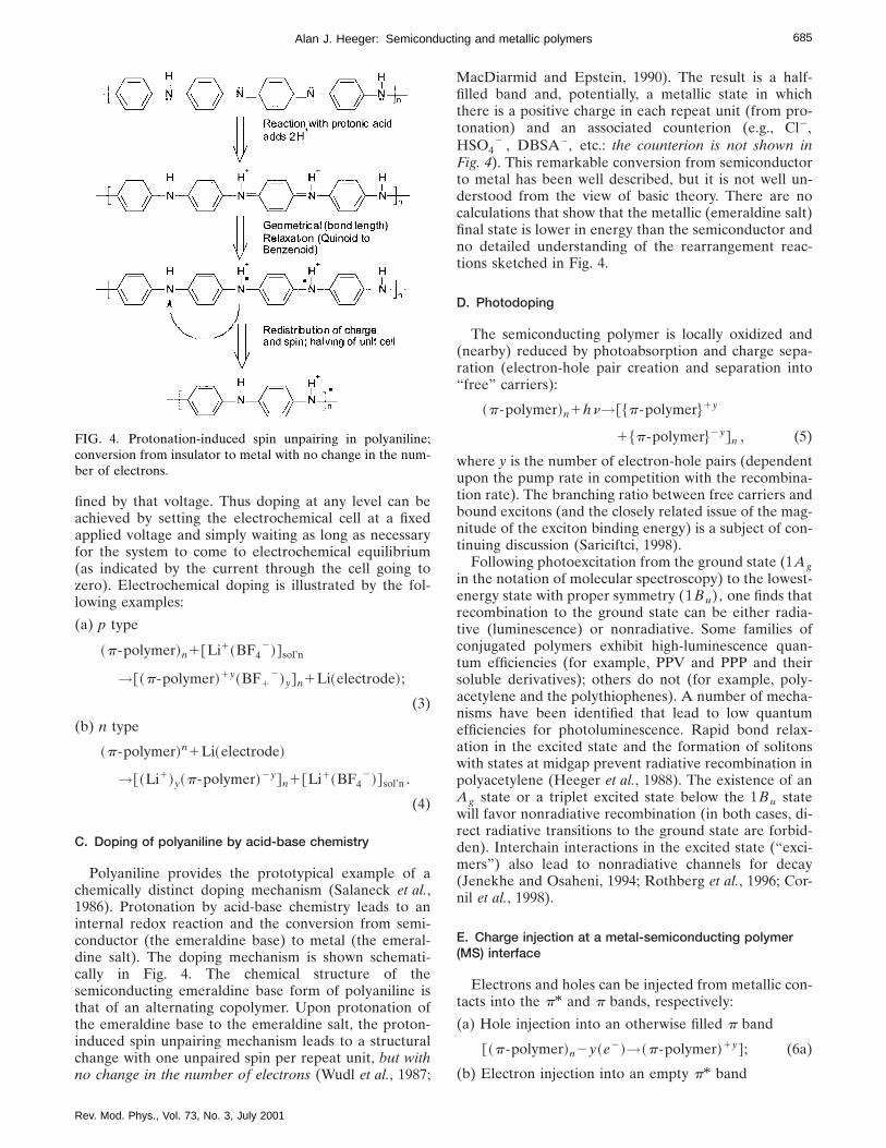
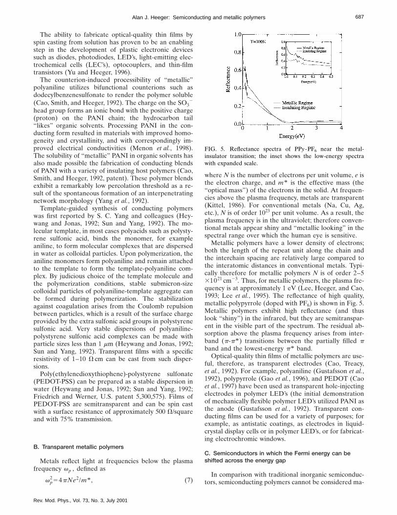


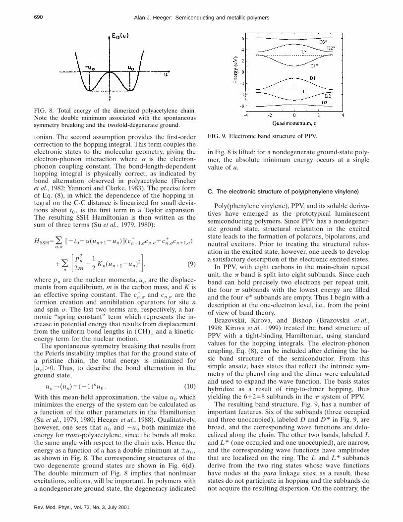
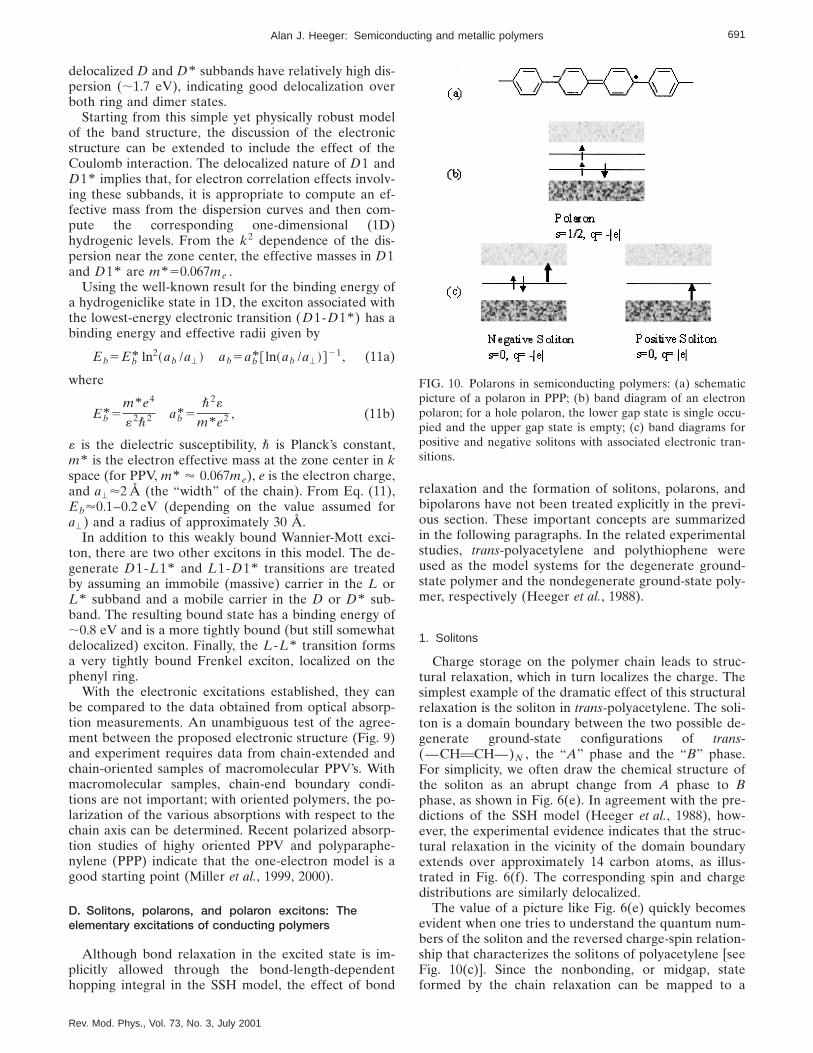


![arXiv:1301.0524v1 [cond-mat.mtrl-sci] 3 Jan 2013The combination of nanoparticles, either metallic [30{32] or semiconducting [33{35], with CNTs nds increas-ing interest due to the anticipation](https://static.documents.pub/doc/80x56/5f0b41877e708231d42f9d8d/arxiv13010524v1-cond-matmtrl-sci-3-jan-2013-the-combination-of-nanoparticles.jpg)


