24
Vol. 15, No.1 – Vol. 16, No. 4 A Bulletin of the Indian Laser Association One more Nobel prize for Lasers Nobel Prize in Physics 2005

Vol. 15, No.1 – Vol. 16, No. 4A Bulletin of the Indian Laser Association
One more Nobel prize for Lasers
Nobel Prize in Physics 2005

ILA Executive Committee
PresidentP.D. Gupta, CAT, Indore
Vice PresidentV.K. Mago,BARC, Mumbai
Gen.Secy. IV.P.N. Nampoori,CUSAT, Kochi
Gen.Secy. IISatya Ram Mishra,CAT, Indore
TreasurerH.S. Vora,CAT, Indore
Regional RepresentativesR. Vijaya,IIT, MumbaiSuranjan Pal,LASTEC, DelhiVasant NatarajanIISc, BangaloreS. Khijwania,IIT,GuwahatiKamal Das,CGCRI,Kolkata
Corporate RepresentativeLaser Spectra Services,Bangalore
Editor
L.M. Kukreja (CAT, Indore)
Editorial Board
K. Dasgupta (BARC, Mumbai)
P.K. Datta (IIT, Kharagpur)
S.P. Gaba (IRDE, Dehradun)
P.K. Gupta (CAT, Indore)
A.K. Nath (CAT, Indore)
P. Radhakrishnan (CUSAT, Kochi)
H. Ramchandran (RRI, Bangalore)
P. Ramamurthy (University of Chennai)
G. Ravindrakumar (TIFR, Mumbai)
BVR Tata (IGCAR, Kalpakkam)
R.K. Thareja (IIT, Kanpur)
K. Thyagrajan (IIT, Delhi)
Editorial Working Committee (CAT, Indore)
Tarun Sharma Rajiv Jain
K.S. Bartwal A. K. Sharma
P. K. Mukhopadhyay J. Jayabalan
S. V. Nakhe C. P. Paul
N. Ghosh P. Mishra
Sendhil Raja
This photograph shows the essential elements of the optical frequency comb synthesizer used by Theodor Hänsch and colleagues at the Max Planck Institute for Quantum Optics in Garching, Germany. An optical frequency comb can measure the frequency of light with extreme precision which is expected to redefine "the second" . Second harmonic of a diode pumped solid state laser (green light) shown on the right side pumps a femtosecond Ti-sapphier laser (middle box). A rainbow of spectral colors is generated by passing the femtosecond pulse into a micro-structured quartz fibre. (Photo courtesy of R. Holzwarth and T. W. Hänsch.)
Cover Photo :
Editorial Team of
Letter from ILA president 1
From the Editor 2
Commentary
World Year of Physics 2005 3
thThe 75 anniversary of Nobel Prize to Sir C.V. Raman 4
Cover Story
Nobel Prize in Physics for 2005 5
From Indian laser laboratories 6
Feature Articles
Crystal Growth of Optical Materials 8
Pyramidal Nanostructures of ZnO 14
Symposium Report
rdDAE-BRNS 3 National Symposium on Pulsed Laser Deposition 16of Thin Films and Nanostructured Materials (PLD-2005)
ILA Membership Form 19
Vol. 15, No.1 – Vol. 16, No.4
Contents
ILA Web pages
We are glad to announce that ILA web pages are now hosted on an independent web server at http://www.ila.org.in. We also have Shri Rajiv Jain, as our new webmaster. He has already introduced some new features in the ILA web pages. One notable feature being “Discussion Group”. All ILA members are invited to join this technical discussion group to exchange professional knowledge related to lasers. Our endeavor will be to make ILA web pages highly interactive and informative. We look forward to your cooperation in achieving this goal.
Prasad A. Naik, CAT Indore Chairman, ILA Web Page Committee

Dear Colleagues,
It is a pleasure to share a few words with you through “Kiran”: Bulletin of the Indian Laser Association (ILA). Sometime ago, Shri T.P.S. Nathan, who was elected as President of the Association for the April 2005 to March 2007 term decided to relinquish this post. Thereupon, earlier this month, the Executive Committee nominated me for the post of President, which I have humbly accepted.
The Indian Laser Association was established in December 1987 and it gained strength year after year. Its present membership exceeds 750. What the Association is today is due to the selfless contributions of many distinguished scientists in the earlier executive committees. They guided the growth of the Association and evolved the spectrum of its activities. It will be our endeavour to enrich it further.
As per the established tradition, the ILA co-organizes the annual DAE-BRNS National Laser Symposium. This year the symposium will be held at Vellore Institute of Technology, Vellore from December 7- 10, 2005. The Annual General Body Meeting of the Association will be held during this symposium. This will give us an opportunity to share our perception and views on the state of progress in the area of lasers and allied fields, and to discuss in what way the Association can further enhance its role in increasing the interaction among the laser fraternity.
The instrument through which the Association reaches its members is its bulletin Kiran. Dr L M Kukreja has now taken over as the Editor of Kiran. There is also a change of guard in the Editorial Board and in the Editorial Working Committee. I am happy that the new team has responded very enthusiastically by resuming the publication of Kiran and bringing out the present issue in a very short time so that it reaches the members prior to the General Body Meeting. I believe that publication of Kiran will continue regularly. Further, keeping up with the times, a web-site for the ILA has also been created on a commercial server. Your suggestions on the possible contents of the web-pages and on the role it can play will be helpful in making it effective and purposeful.
For the benefit of students and young researchers, the Association organizes some courses. This year three short tutorial courses are being organized preceding the National Laser Symposium. Next, the Association will also award prizes for the best thesis and poster presentations made at the Symposium. It will also organize an exhibition of various laser related equipments manufactured/supplied by Indian companies.
The real strength of any association lies in the active involvement of its members in its affairs. I look forward to your enthusiastic participation and continued support to the Association for it to usher in a future which is brighter than the successful past.
With best wishes and warm regards,
P. D. GuptaNov. 19, 2005
LETTER FROM ILA PRESIDENT
1

It is indeed a pleasure to bring out this issue of ‘Kiran’ after a gap of nearly two years. We will strive to publish it regularly every four months. ‘Kiran’ is not only a news bulletin of the Indian Laser Association; it provides a forum for professional interactions amongst the members and generates awareness of the ongoing developments in the country. Since this bulletin is of, for and by the Indian scientific community, we will widen the coverage of quality Indian accomplishments in the arena of laser science and technology in our column on ‘News watch’. At the same time, extraordinary international developments pertinent to the field of lasers and allied areas will also find place in the pages of ‘Kiran’ from time to time. We intend also to present a broader national scenario of the field in the future issues of this bulletin. The members and their colleagues are therefore requested and encouraged to keep us informed about the scientific developments at their end and contribute articles of interest to the community on a regular basis. To broaden the scope of features covered by this bulletin we shall welcome articles not only of general interest but also book reviews, tutorial articles, views about any specific area of research and development, correspondence etc. To be prudent about our scarce financial resources we will like to give ‘Kiran’ a rather simple look without sacrificing its contents.
As we know, Physics Nobel Prizes for the year 2005 have been conferred on Roy J. Glauber ‘for his contribution to the quantum theory of optical coherence’ jointly with John L. Hall and Theodor W. Hänsch ‘for their contributions to the development of laser-based precision spectroscopy, including the optical frequency comb technique’. Since this event is of prime interest to the laser community globally, this has been selected as the cover story for this issue of ‘Kiran’. Besides this we have included a few articles and the regular features of this bulletin and a short report on recently concluded DAE-BRNS meeting on Pulsed Laser Deposition of Thin Films and Nanostructured Materials (PLD-2005).
This issue was brought out in a short span of less than a month. I wish to put on record my appreciation of the untiring efforts of the editorial working committee members, which made this possible. I also wish to thank Dr. S. C. Mehendale and Mr. Tapas Ganguly for their help during preparation of this issue.
‘Kiran’ is the bulletin that belongs to all of us. Its value, growth and sustenance are our collective responsibility. I therefore look forward to your valuable suggestions and active participation.
Lalit M. Kukreja November 20, 2005
FROM THE EDITOR....
2

Commentary
World Year of Physics 2005
The World Year of Physics is being celebrated throughout the year 2005, round the globe to commemorate one hundred years of seminal papers of Albert Einstein in 1905 on Relativity, Photoelectric effect and the Brownian motion. The effort is led by the United Nations, through a General Assembly Resolution on June 10, 2004. The International Union of Pure and Applied Physics declared the year 2005 as the World Year of Physics. With this declaration, people all over the world are joining in this celebration. This year provides the opportunity to celebrate Einstein, his great ideas, and his influence on life in the 21st century. The World Year of Physics (WYP 2005) is a worldwide celebration of physics and its importance in our everyday lives. Physics not only plays an important role in the development of science and technology but also has a tremendous impact on our society. World Year of Physics aims to raise the worldwide awareness of physics and physical science.
In 1905, Albert Einstein wrote three fundamental papers, all in a few months time. The first paper claimed that light must sometimes behave like a stream of particles with discrete energies, “quanta” - Photoelectric Effect.. The second paper offered an experimental test for the theory of heat- Brownian Motion. The third paper addressed a central puzzle for physicists of the day – the connection between electromagnetic theory and ordinary motion – Special Theory of Relativity.
Einstein was much ahead of his time. It is impossible to overstate the importance of what Einstein did in 1905. His work on Brownian motion provided the theoretical framework for experiments to prove that atoms were real. Hard as it might be to believe now, at the time the majority of physicists did not believe in atoms. The
2special theory of relativity completely changed our notions of space and time, while E=mc led to the remarkable conclusion that mass and energy are one and the same. And his work on the photoelectric effect was the start of a love–hate relationship with quantum mechanics that still fascinates physicists today. And 1905 was just the beginning. The general theory of relativity – his truly outstanding achievement – followed 10 years later, with its predictions for the bending of light by mass being confirmed a few years after that during the solar eclipse of 1919. But even then Einstein did not abandon his interest in atoms, photons and quantum mechanics. The Einstein A and B coefficients for spontaneous and stimulated emission – without which we would not have lasers – made their debut in 1916, and the prediction of Bose–Einstein condensation – one of the hottest topics in experimental physics for the past decade – followed in the 1920s.
The Indian Physics Association (IPA) has been organising several events since January 2005 to celebrate the occasion and joining hands with several like-minded societies. Dr. R. Chidambaram, Principal Scientific Advisor to the Government of India & DAE Homi Bhabha Professor is the Chairman of the National Co-ordinating Committee. The World Year of Physics 2005 plans to bring the excitement of physics to the public and inspire a new generation of scientists. Timed to coincide with the centennial celebration of Albert Einstein’s “miraculous year,” the World Year of Physics will be coming to YOU before you know it.
At the end one quote from Einstein about science: “One thing I have learned in a long life: that all our science, measured against reality, is primitive and childlike—and yet it is the most precious thing we have”.
K.S. Bartwal, CAT Indore.
3

Commentary
thThe 75 anniversary of Nobel Prize to Sir C.V. Raman
The 75th anniversary of Nobel Prize of Sir C.V. Raman, first and only Indian citizen to win a Nobel in science, is being celebrated this year. The first ‘Indian Nobel’ for science is thus 75 years old. Raman remains the only Indian to receive a Nobel Prize in science. Two Indian-born scientists, Har Gobind Khorana and Subrahmanyan Chandrasekhar, won Nobel Prizes, but they had become U.S. citizens. February 28, the date on which Raman’s discovery was reported, is observed as National Science Day in India. He was a genius right from his childhood. Chandrasekhar Venkata Raman, popularly known as C.V. Raman, was born in Tiruchirapalli, Tamil Nadu, on November 7, 1888. At 15 years of age, he finished his B.A., winning the first place and gold medal for physics. He was barely 17 when he received his M.A. degree in 1907.
In 1917 Raman was offered Sir Taraknath Palit Professorship in Physics at Calcutta University. He became a fellow of the Royal Society of London in 1924. He was made a knight of the British Empire in 1929. The following year the Royal Society honoured him with the prestigious Hughes Medal.
In the summer of 1921, Raman’s voyage to Europe sailed through Meditarrean Sea. During this voyage, he observed with wonder brilliant blue colour of the Mediterranean, and later the blue colour of glaciers. This
thobservation gave birth to an idea, which became basis for the historic experiment of 28 Feb. 1928. Raman and his students, especially K.S. Krishnan, began studying the phenomena. Krishnan attempted to record the effect of scattering of light in various mediums throughout February in 1928. On February 27, he observed a definite, faint greenish glow in glycerine and reported it. Raman set out to study the “mysterious” greenish glow on the morning of February 28. That experiment resulted in a discovery: “ Change of Wavelength in Scattering”. This is the famous “Raman Effect”. For this discovery he was awarded Nobel Prize in 1930. The genius won the Nobel Prize for Physics, with simple equipment barely worth Rs. 300. He was a man of boundless curiosity, his spirit of inquiry and devotion to science laid the foundations for scientific research in India.
In 1934, Raman became the director of the newly established Tata Institute for Science (currently the Indian Institute of Science) in Bangalore, where two years later he continued as a Professor of physics. In 1947 he was appointed the first National Professor by the new government of independent India. He retired from the IISc in 1948, and a year later he established the Raman Research Institute in Bangalore. He served as its director and remained active until his death on November 21, 1970, at the age of 82. For all of us, it is appropriate that Raman is remembered in this year not only for the 75th anniversary of his Nobel Prize but also for his contribution to physics.
K.S. Bartwal, CAT, Indore
4

Light exhibits a dual nature – it can be considered both as waves and as a stream of particles. Roy Glauber has established the basis of Quantum Optics, in which quantum theory encompasses the field of optics. He could explain the fundamental differences between hot sources of light such as light bulbs, with a mixture of frequencies and phases, and lasers which give a specific frequency and phase. It would not be an exaggeration to say that this work laid the foundation of modern day Quantum optics. His work on Quantum coherence and coherent states of radiation field lead to the discovery of several new Quantum optical effects like anti-bunching of photons and squeezed states of light.
After the discovery of masers, it was realized that photon correlation experiments with this light and for Hanbury Brown and Twiss (HBT) type photon correlation experiments, the classical theory of optical coherence is inadequate and a quantum theory of optical coherence is necessary for the description these experiments. In three papers, first in Physical Review Letters followed by two detail papers in Physical Review, Glauber formulated the theory of quantum coherence and coherent state of quantized electromagnetic field. For this purpose he first analyzed the quantum theory of the photo-detection process. Using these results for the quantum photon detection rate he introduced hierarchy of quantum field coherence functions. Using this hierarchy of coherence functions he also formulated the criterion for the coherence of quantum states of radiation field. He could explain the results of HBT experiment by studying the second-order coherence function. The next question, which was answered in these papers, was which quantum mechanical field state can be considered analogous to the classical stable wave or coherent wave. For such stable waves the
The Royal Swedish Academy of Sciences has decided to award the Nobel Prize in Physics for 2005 with one half to Roy J. Glauber Harvard University, Cambridge, MA, USA “for his contribution to the quantum theory of optical coherence” and the other half jointly to John L. Hall, JILA, University of Colorado and National Institute of Standards and Technology, Boulder, CO, USA and Theodor W. Hänsch Max-Planck-Institut für Quantenoptik, Garching and Ludwig-Maximilians-Universität, Munich, Germany “for their contributions to the development of laser-based precision spectroscopy, including the optical frequency comb technique”.
classical theory of coherence says that coherence functions to all orders yield unit values. Glauber introduced the eigenstate of the photon annihialtion operator and showed that field in these states yield unit values of coherence functions to all orders. He termed these eigen states of photon annihialtion operator as “Coherent states” of radiation field. These coherent states played an important role in the development of Quantum optics. Using coherent state representation he introduced the P-function or the Glauber-Sudershan representation which renders a diagonal representation for the density matrix of the optical field. The P-function serves the purpose of a probability function , which can be employed to calculate the averages of the normally ordered field observables. The non-existence of P-function for a state of radiation field signifies that the state does not have any classical analogue and it is purely quantum mechanical in nature. The anti-bunched and squeezed lights belong to the category of quantum or non-classical light. In the later development Quantum optics these non-classical lights have been generated in several laboratories.
The important contributions by John Hall and Theodor Hänsch have made it possible to measure frequencies with an accuracy of fifteen digits. Lasers with extremely sharp colours can now be constructed and with the frequency comb technique precise readings can be made of light of all colours. This technique makes it possible to carry out studies of, for example, the stability of the constants of nature over time and to develop extremely accurate clocks and improved GPS technology.
Communicated by: Arup Banerjee, J. Jayabalan and Sendhil Raja, CAT, Indore
Nobel Prize in Physics 2005
5
Cover Story

From Indian Laser Laboratories
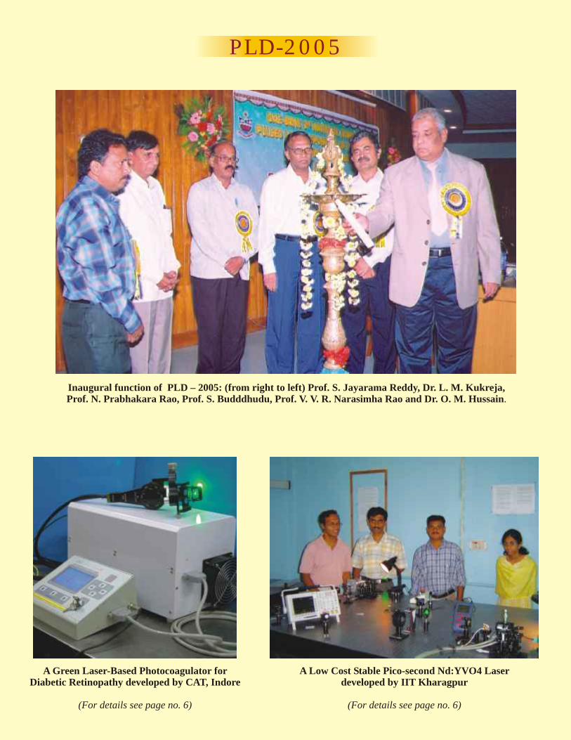
Green Laser based Photocoagulator for Diabetic Retinopathy
CAT, Indore has developed laser-based photocoagulator, which would be used to treat patients diagnosed with diabetic retinal disorder- a medical condition where one losses vision after bleeding in the retinal veins. The laser beam which is green in colour can reach to the retina without much absorption at the intermediate ocular media and gets absorbed at the retina enabling controlled cutting and blocking of the excess blood vessels resulting from this disease.
The unit ( see photograph) is a unique combination of laser physics and engineering. It has main three parts: (i) laser, (ii) driver and control and (ii)beam delivery system. The Nd:YVO crystal based laser is pumped axially by 4
a fiber coupled laser diode to generate beam at
1.06mm. The wavelength was then halved by placing a nonlinear crystal (KTP) inside the cavity to generate green laser light at 532 nm. The laser
cavity was highly compact and its temperature was precisely controlled for reliable operation. It was driven by a microprocessor based unit to control the output power and width of the rectangular green pulse as per the requirement for the treatment. The beam is coupled to the beam delivery system which contains an optical fiber and optics to vary the spotsize at the retina. A low power visible diode laser is also incorporated to aim at the location where the green laser beam would be launched.
In September of this year CAT handed over this unit to M/s AuroLab, a part of Arvind Eye-Care Hospital, Madurai, as per the MOU signed between them.
(See the photograph of unit at inside of back cover page)
Communicated by P. K. Mukhopadhyay, SSLD, CAT, Indore
A Low Cost Stable Pico-second Nd:YVO Laser4
Indian Institute of Technology, Kharagpur has developed a simple, efficient and low cost cw mode-locked pico-second Nd:YVO laser. The 4
mode-locking which relies on the nonlinear mirror technique, is stable, self-starting, self-sustained and power scalable. The group headed by Dr. P K Datta had started their programme of developing the laser at the Department of Physics & Meteorology in 2002 under a small funding form DST and DRDO. According to Dr. Datta ‘the nonlinear mirror is realized by an assembly of a second harmonic generation crystal and a dichroic mirror. It produces the saturable loss in the laser cavity. The mode-locked pulse we achieved is of width 9ps. We could also achieve a peak power of 280kW for the pump power of 10W, by running the laser in actively Q-switched and nonlinear mirror mode-locked regime. [Appl. Opt., 43, (2004) 2347; Opt. Commun., 230, (2004) 411; Opt. Exp., 12, (2004) 4041].’ Mr S.
Mukhopadhyay, a senior research fellow of the group says ‘the major break through came out when we incorporated a third harmonic generating crystal to realize inverse loss saturation. Now our laser gives very stable cw mode-locked pulse train and never affected by passive Q-switching instability.[ Appl. Phys. Lett., 86, ( 2005) 151105]’ Prof. A Agnesi, the Italian collaborator of Dr. Datta, says ‘ the inverse saturable nonlinear mirror as demonstrated by the group of Dr. Datta is, in my view, the simplest technique to generate stable mode-locked pulse train.’ A part of the work was presented in the session ‘Novel Techniques for solid state lasers’ at CLEO (USA), 2005.
(See the photograph of unit at inside of back cover page)
Communicated by P. K. Datta, IIT Kharagpur
6

High Quality ZnO/MgZnO Quantum Wells Grown by Pulsed Laser Deposition at CAT, Indore
Third harmonic of Q-switched Nd:YAG laser based Pulsed Laser Deposition (PLD) technique has been applied to grow high quality quantum wells of ZnO [1]. ZnO, which is a wide and direct bandgap (~ 3.3 eV) II-VI oxide semiconductor with remarkably high excitonic binding energy (~ 60 mV) and possibility of bandgap engineering through metastable alloying for the realization of nanostructures, is currently of immense interest for the development of Light Emitting Diodes, Diode Lasers, solar blind photo-detectors and spin photonic devices operating in the UV-blue spectral region. The putative optical quantum confinement effects have been observed in the CAT ZnO multiple quantum wells (MQW). A novel in-house developed buffer assisted growth methodology [2] was used to achieve high crystalline and optical qualities of these nano-structures at comparatively low growth temperatures which also helped in maintaining chemically sharp interfaces as the inter diffusive processes at the interface were highly subdued at low temperatures. A 10 layer MQW structure was
grown with 8 nm thick ternary alloy Mg Zn O 0.16 0.84
layer with a band gap of ~ 4.1 eV as a barrier and the active layer of ZnO had variable thickness in the range of 5 – 1 nm. The room temperature optical absorption spectra of these samples showed a clear blue shift in the ZnO absorption edge with decreasing well layer thickness up to 1 nm due to the size dependent quantum confinement effects. The PL at 10K due to excitonic recombination in ZnO QW was observed in all the samples as shown in figure 1. PL spectra of these samples showed a clear blue shift in the ZnO band edge from ~ 3.4 to ~ 3.7 eV with decreasing well layer thickness. Room temperature PL in the UV spectral range was also observed for the MQW samples up to 2 nm of well thickness bellow which the PL signals was too weak to be detected. Perhaps these are some of the thinnest ZnO Quantum Wells grown on sapphire using PLD, which showed quantum confinement effects and room temperature photoluminescence.
References :1. P.Misra, S. Porwal, T. K. Sharma and L. M. Kukreja, Growth of ZnO/MgZnO Multiple Quantum Wells by
rdPulsed Laser Deposition, Proc. 3 Intl. Workshop on ZnO and Related Materials, Oct. 5 – 8, Sendai, Japan 95 (2004)
2. P.Misra and L. M. Kukreja, Buffer Assisted Low Temperature Growth of High Crystalline Quality ZnO Films using Pulsed Laser Deposition, Thin Solid Films, 485 (1-2), 42-46, (2005).
Communicated by: P. Misra, Tarun Sharma and L. M. Kukreja, CAT, Indore
7

Crystal Growth of Optical Materials
This article reviews important methods of preparing single crystals of optical materials for variety of
applications in laser technology. In order to demonstrate as to how the phase and crystalline purity necessary
for best device performance can be achieved by optimizing the growth parameters, some results on the
preparation and characterization of borates are presented.
1. Introduction
The performance characteristics of different crystal ingots of a given material prepared under more or less identical conditions are often found to show large variations. This fact can be attributed to a number of factors such as, (i) the technique and the preparatory conditions employed, (ii) purity of the starting materials used, (iii) stoichiometric deviations, (iv) the presence of other phases in the phase diagram, etc. The formation of lattice defects which act as quenchers is mainly governed by the method of preparation and the preparatory conditions employed. While, a particular material may be prepared in number of ways, the selection of the one that produces an end product of better crystalline purity is important. The lattice defects of concern here are the dislocations, precipitates, point defects, cracks etc. The presence of impurities in the lattice is invariably of serious concern. Very often the impurity levels do not have to be very large to give rise to frequently observed crystal coloration. The crystal coloration has a detrimental effect on the luminescent properties of the crystals. In the case of mixed oxide crystals, the constituent oxides may have quite different vapor pressures at the processing temperatures and consequently the composition of the grown crystal deviates from stoichiometry. The stoichiomtric deviations may influence the optical and the luminescent properties [1]. The situation gets further complicated if more than one phases are present in the phase diagram of the material.
For several important applications like solid state lasers, non-linear optical elements, transmitting windows, pyroelectric detectors etc., the materials are required in the form of high quality single crystals. In Table 1 some important crystals and their applications have been listed.
Table 1: Applications and crystals
Transmitting WindowsAlkali halides, alkaline earth fluorides,Ge, ZnS, ZnSe, GaAs, GaP, Al O2 3
Nonlinear OpticsBaB O , LiB O , KTiOPO ,2 3 3 5 4
LiNbO , KH PO3 2 4
Solid State Laser Materials Y Al O (Nd),Gd Ga Sc O (Cr,Nd),3 5 12 3 3 2 12
YVO (Nd), LiYF (RE), LiCaAlF (Cr), A O (Ti)4 4 6 l2 3
PyroelectricsPb Ge O , LiTaO ,5 3 11 3
In this article, we first survey the techniques conventionally used for the preparation of single crystals. A brief evaluation of the techniques from a personal perspective will be given. We will also show as to how the processing conditions can influence the formation of impurity phases, particularly in the case of some borate materials.
2. Material Preparation Techniques
The process of crystal growth essentially involves a change of phase where the molecules of the material undergoing the change of phase are gradually, uniformly and continuously losing their random character achieve the long range order. A number of techniques for the preparation of crystalline materials have been developed essentially to suit the requirements of different materials and to achieve the required crystalline perfection for their intended applications. The important techniques available have been summarized in Table 2. The Bridgman or different variants of this technique are particularly suitable for the single crystal growth of fluorides and other halide crystals. The predominant use of Czochralski pulling technique is for oxide and
8
Feature Articles

similar materials. The solution growth, both from aqueous medium and the molten salt solutions, as well as the hydrothermal growth technique are suitable for special cases. The second column in Table 1 shows the utility factor for various techniques listed. In the following we shall briefly discuss these techniques.
Table 2: Methods of crystal growth
2.1. Bridgman Technique
The crystal growth is effected in a suitable container by lowering the melt through the melting point isotherm along a gradient in the furnace. Suitable temperature profile can be obtained (i) by constructing a two zone furnace in which the temperatures of both the zones are controlled with the help of two thermocouples placed at suitable locations [2] and (ii) employing a single zone with graded winding [3]. The choice of materials as the heating element, thermal insulation, thermocouple etc. depends upon whether the growth is to be effected under normal ambient, static or dynamic vacuum. Commonly used heating elements for application under normal ambient include nichrome or kanthal. For growth under dynamic vacuum conditions, the hot zone is developed using the heating element fabricated from high density graphite or molybdenum. In order to obtain the desired thermal gradient and also for the purpose of thermal shields, molybdenum and stainless steel cylinders surrounding the heater are usually employed.
In absence of a seed crystal, the supercooled melt does not solidify until degree of super-cooling is sufficiently large to give rise to the appearance of solid phase in the melt. Once the melt nucleates, the remaining mass is capable of undergoing a phase change in a continuous
manner. In order to grow a single crystal, it is imperative that a single nucleus propagates throughout the melt. This can be achieved by controlling the direction and amount of heat flow in such a way that no further nucleation occurs on the growing solidmelt interface. This requires stable thermal conditions in the furnace during the growth. Apart from growth rate, macroscopic solid-melt interface shape is an important factor determining the generation and propagation of defects during crystal growth. The macroscopic shape of the interface achieved in practice depends upon the thermal conditions that exist in the furnace, physical properties of the material in both molten and solid state and the growth velocity. In fact, a plane interface is desired as it helps in minimizing the generation of thermal stresses during growth. However, in practice, a slightly convex shape interface is preferred for better grain selection and to avoid secondary nucleation at the crucible walls. This can be achieved by properly positioning the freezing plane in the furnace. In order to standardize the growth parameters and select thermal characteristics of the furnace conducive for good growth, several thermal models have been developed. They enable to compute the axial and radial temperature profiles, the effect of crucible material, thermal conductivities in crystalline and molten states.
For the growth of alkali halide or alkaline earth fluoride crystals up to 50 mm diameter, an
-1axial thermal gradient of 20 deg cm and the
-1lowering rate of 1 mm h are quite suitable. The temperature stability of the furnace should be
close to ± 1 degree. For alkali halides, cooling -1
rates of ~ 20 deg h are found suitable. Whereas, alkaline earth fluorides require cooling rates of 15
-1deg h or lower. The presence of oxide impurity in fluoride crystals gives rise to cracking. It is therefore very important to control the presence of this impurity in the crystal [4].
2.2. Czochralski Techniqe
The crucible containing material is heated by a suitable means (RF, Joules effect etc.) so that a clear melt is obtained. A seed crystal of the same material is slowly brought in-contact with the melt. The melt temperature is so adjusted
Bridgman type
Czochralski pulling
Solution growth (aqueous
medium, molten salt,hydrothermal)
20
70
10
Method Utilityfactor (%)
9

that thermodynamical equilibrium between the seed and the melt is established. Subsequently, the seed is slowly pulled upwards to effect crystal growth. The crystal is kept continuously rotated to achieve thermal symmetry at the growing interface. The design of growth station assumes special significance for crystal growth by this method, as it controls the heat loss. The generation and propagation of defects is governed by the shape of the solid-melt interface which is a function of the heat loss. Hence, the heat transfer paths and their control are important to realize the growth of defect free crystals. Other sources of temperature fluctuations of inherent nature present in Czochralski configuration are (i) random turbulence, (ii) non-coincidence of rotational and thermal axes and (iii) mechanical vibrations. Because of the presence of these intrinsic instabilities different schemes have been developed to control the growth rate. They are based on crystal or crucible weighing and the use of optical reflection from meniscus. The basic philosophy behind these controls is to sense the variations in the growth rate arising due to the cumulative effect of various factors and accordingly modify the heat input to the crucible. In addition to the heat transfer paths, crystal rotation rate, pull rate and macro/micro-segregation effects are the important growth parameters. For a crystal pull rate of P, the growth rate (R) achieved in practice is given by Eq. 1. The growth rate is a function of the crystal (D ) and s
crucible (D ) diameters and the densities in the c
molten (r ) and solid (r ) states. m s
2R = P / [1- (r / r ) (D / D ) ] …..(1) s m s m
The upper limit for the pull rate is determined by (i) thermoelastic properties of the crystal, (ii) segregation of dopant / impurity ions at the growth interface and their diffusion to the bulk and (iii) ease with which defects can be generated during growth. The materials having high thermal conductivity and Burger vector like Y Al O (YAG) or Al O can be pulled at 3 5 12 2 3
relatively faster rates, provided segregation effects are not the limiting factor. The upper limit for the pull rate in this case is decided by the temperature gradient that can be maintained above the solid–melt interface. The maximum
acceptable axial temperature gradient can be computed using Eq. 2.
3/2 0.5[dT/dZ] = [4 e /a r ] [h] [1–0.5 h r ] …..(2)max b
where, e is the breaking strain, a is the expansion b
coefficient, h is the cooling constant (ratio of the rate of heat loss per unit area per degree excess temperature above the ambient to the thermal conductivity) and r is the crystal radius. Besides other factors, the value for maximum axial temperature gradient depends on the crystal radius. When the crystals are doped with desired ions then the growth parameters are governed by the mass transport taking place at the solidmelt interface. The maximum growth rate in this case is a function of the distribution coefficient of the dopant in the crystal lattice. For example, undoped YAG crystals can be grown at high rates of 2 to 4 mm/h whereas very low growth rates (0.5 mm/h) must be employed for YAG(Nd) crystal [5]. This is because of the low segregation coefficient of Nd (0.18) in YAG lattice. The crystal cracking is a common problem faced with the growth of most insulating crystals. The stresses arising due to the temperature gradient built into the crystal during growth and cooling are primarily responsible for this defect. The problem is particularly serious if the crystal has anisotropic contraction and the presence of a cleavage plane. In this case the crystal must not be cooled at a rate greater than that given by Eq. 3.
2[dT/dt]max = k e / a r …….(3) b
where, k is the ratio of the thermal conductivity to specific heat per unit volume. The growth in all such cases should be effected under low axial thermal gradient and along the axis that has smaller expansion coefficient [6]. The Pb Ge O 5 3 11
(LGO) crystals which possess good pyroelectric properties and hence find application in the fabrication of pulsed laser energy / power meters is known for its low thermal shock resistance. Figure 1 shows a typical crystal ingot of LGO grown along a specific direction to avoid the problem of cracking.
10

The crystal growth of several other technologically important laser materials namely Gd Ga Sc O (Cr, Nd) (GSGG), LiYF (RE), 3 3 2 12 4
LiCaAlF (Cr), YVO (Nd) is also carried out by 6 4
this technique. The growth of fluoride crystals must be carried out either under CF or H 4 2
atmospheres to ensure complete removal of oxygen from the growth chamber. The presence of even minute amount of water or oxygen is highly detrimental to crystal quality. The GSGG shows strong tendency to grow in the form of spiral as shown in Fig.2. The problem can be overcome by selecting proper temperature gradients and the growth parameters [7].
2.3. Top Seeded Solution Growth Techniques
This method is usually preferred when growth from melt is not possible for some reasons and also the material does not have a suitable solvent for low temperature solution growth but the growth can be effected from a molten salt solution. The material mixed with flux in the desired ratio is placed in a crucible and heated to obtain a clear solution. The temperature profile established is such that just above the solution surface a proper temperature gradient exists. Like in Czochralski configuration, a seed crystal is brought from top and touched to the solution. The growth is achieved by slowly pulling the seed (1
-1mm d ) and simultaneously cooling the solution
-1at very slow rate (1 to 2 deg d ). The furnace configuration, solution composition, crystal pull and temperature lowering rates are the important growth parameters. The growth of well known
non-linear optical crystals like b-BaB O (BBO), 2 4
incongruently melting LiB O (LBO) and 3 5
KTiOPO (KTP) crystals are the typical examples 4
of growth by this technique. BBO melts ocongruently at 1099 C and crystallizes into a-
phase. There is another phase of BBO namely b-o
phase which is stable only below 925 C. The
kinetics of transformation from a - b is quite slow
and hence the bphase cannot be easily grown from melt. The growth in this case can be carried out by TSSG technique using Na O as a flux [8]. The 2
single crystals of LBO are grown using a boron oxide composition [9] and those of KTP using K W O as a flux [10].2 2 7
3. Crystal Growth and Characterization of Borates
3.1. BaB O2 4
Beta-BaB O (b-BBO) crystal is one of 2 4
the most prominent materials currently in use for the generation of second and higher harmonics of
1.064 mm emission from Nd:YAG lasers. Recently, the generation of tunable deep UV radiation down to 187.9 nm in this crystal has also been demonstrated. BBO melts congruently at
o~1100 C and from melt, normally the growth of a-
Fig.1: LGO crystal grown along <001>
Fig.2: A photograph of GSGG showing spiral and parallel growth.
11

phase crystals can only be effected. This is
because the rate of transformation from a to b-phase is quite slow and also the structural re-
oordering around 925 C results in crystal cracking.
Consequently, the crystal growth is carried out by TSSG technique using Na O as a 2
flux. This must be done under minimum value for -1
the vertical thermal gradient (~20 deg. cm ) to avoid the entrapment of flux as tiny scattering centers distributed throughout the volume. The solution compositions consisting of BBO and Na O in the ratio of 81:19 are found to be most 2
favorable for good growth. For a solution of about 70 cc volume, the optimum crystal pull and
-solution cooling rates are of the order 0.016 mm h1 -1 and 0.1 deg. h , respectively. The crystals grown
under these conditions are generally found to have sodium contamination in the range 100-200 ppm. The sodium contamination gives rise to the presence of chargetrapping sites close to the band edge whereby it gives rise to optical absorption and the effect is most significant in the UV region. The ESCA analysis shows that the binding energies of oxygen, barium and boron core levels are influenced by the presence of sodium, implying its substitution into the crystal lattice [11]. The crystal hardness for optical damage is also affected by the presence of this impurity. Consequently, efforts have been made to grow the crystals by Czochralski technique [12,13].
3.2. LiB O3 5
LiB O (LBO) phase decomposes into 3 5
Li B O (247) and Li B O (2813) at the melting 2 4 7 2 8 13
temperature and hence crystal growth is carried out by TSSG technique using boron rich charges. The presence of small amount of 247 phase in the solution promotes polycrystalline growth of the LBO phase by providing uncontrolled sites for crystallization. On the other hand, large concentrations of the impurity lead to the formation of glassy phase. It is therefore important that the crystallizing medium should be free from the presence of this contamination. This could be achieved by (i) using a well synthesized starting charge for growth, (ii) purification of the LBO phase through recrystallization i.e. using clear crystal chunks obtained from the previously
grown polycrystalline ingots as the starting LBO material for growth and (iii) restricting the highest
osolution temperature to 860 C during the growth. The requirement of restricting the solution
otemperature to 860 C arises for the following reason. When LBO is raised to just a few degrees above the melting point, the melt essentially contains the basic growth units of LBO which are
-1(B O ) groups. Consequently, on cooling the 3 5
crystallization takes place as revealed by the presence of exotherms in Fig. 3. On the other hand, when the melt is heated to temperatures
ohigher than 860 C, the growth units of LBO in the melt get transformed to those corresponding to the phases formed on decomposition of the LBO phase viz. 247 and 2813. The result of Fig. 4 suggests that under the conditions the decomposed phases must be cooling down to RT without any nucleation. The crystal growth under
Fig.3: DTA plot of LBO recorded during cooling o
cycle with melt temperature restricted to 860 C.
Fig 4: DTA plots of LBO obtained over the range 0
100-900 C during (a) heating and (b) cooling cycles.
12

this condition gets inhibited. The detailed investigations carried out show that this is due to the formation of 247 phase. The presence of this impurity phase must therefore be avoided to produce LBO crystals of high crystalline quality.
References
1 S.C. Sabharwal and Sangeeta, J. Crystal Growth 200 (1999) 191.
2. S.C. Sabharwal, T. Mirza, S.C. Karandikar and B. Ghosh, Cryst. Res. Technol., 20 (1985) 837.
3. S.C. Sabharwal, T. Mirza, S.C.Karandikar and B. Ghosh, J.Crystal Growth 80 (1987) 33.
4. S.C. Sabharwal, Sangeeta and A.K.Chauhan, J. Crystal Growth 240 (2002) 473.
5. Sangeeta, S.C. Sabharwal and M.K. Gupta, Proc. Indian Natn Sci. Acad., 57A (1991) 2.
6. S.C. Sabharwal and Sangeeta, J. Crystal Growth, 216 (2000) 535.
1 2S.C. Sabharwal and Sangeeta1 Spectroscopy Division
2 Crystal Technology Section, TPPED
Bhabha Atomic Research Center, Trombay, Mumbai – 400 085
7. Sangeeta and S.C. Sabharwal,XXXII National Seminar onCryatsllography (Jammu Uni., 2002).
8. S.C. Sabharwal and Sangeeta, J. Crystal Growth 187 (1998) 253.
9. S.C. Sabharwal, Babita Tiwari and Sangeeta, J. Crystal Growth 249 (2003) 502.
10. I.Bhaumik, S. Ganesamoorthy, R.Bhatt, R. Sunder, A.K. Karnal and V.K. Wadhawan, J. Crystal Growth 243 (2002) 522.
11. S.C. Sabharwal, Sangeeta, M. Goswami, S.K. Kulkarni and B.D. Padalia, J. Materials Science : Materials in Electronics 11 (2000) 325.
12. Sangeeta and S.C. Sabharwal, J.Crystal Growth 222 (2001) 427.
13. S.C. Sabharwal and Sangeeta, J.Crystal Growth 236 (2002) 667.
13

Pyramidal Nanostructures of ZnO
A frequency tripled pulsed Nd:YAG laser (Quanta-Ray GCR-170, Spectra-Physics, USA) with a pulse width of ~ 5 ns and repetition rate of 10 Hz was used for the ablation of ZnO target. A convex lens of 50 cm focal length was used to focus the laser beam on to the target, through a quartz window fastened to the deposition
-6chamber, held at 10 Torr. The substrate, Si(100) was placed directly opposite to the target at ~5 cm, fastened to a molybdenum boat whose temperature could be varied up to 1500 ºC. Prior
to mounting, the silicon substrate was cleaned using the piranha solution (1:2 H O :H SO ) 2 2 2 4
(Caution: this mixture reacts violently with organic matter) and etched in HF (1:10 HF:H O). 2
The energy of the laser was optimized at 200 mJ per pulse to enable the desired growth of the nanostructures. The deposition was made at different substrate temperatures (600 ºC and 900 ºC) and for different deposition times (15, 30 and 45 minutes) under a pressure of 10 mTorr of oxygen.
Figure 1: AFM images of ZnO deposited for 45 minutes on a Si(100) surface held at 600ºC: (a) height image (b) friction image. (c) Profile analysis of the image in (a), (d) SEM image of the nanostructures collected with the substrate oriented at ~ 5º to the beam.
Atomic force microscope (AFM) and scanning electron microscope (SEM) images of the ZnO nanostructures obtained after 45 minutes of deposition on the Si(100) surface held at 600 ºC, are shown in Figure 1. The topography and friction images shown in Figures 1 a and b respectively reveal complimentary details of the nanostructures. While the presence of micron-sized structures is apparent from the topography image (Fig. 1a), their pyramidal morphology is revealed by the friction image in Figure 1b. The facets and the associated fine structures with sharp edges are clearly seen in the friction image. The line-profiles of two of the nanostructures in
Figure 1c provide a base width of ~ 2 mm and a
height of ~ 1 mm. The SEM image shown in
Figure 1d, contains several such pyramidal structures. Imaging in larger areas has shown that the pyramidal structures vary in a narrow size
range of 1.5 to 2 mm. AFM images show a few small features after 15 minutes of deposition and a longer deposition for 30 minutes clearly produces larger and more number of structures of pyramidal morphology. Though pyramid-like
4surface roughness has been reported, the pyramids observed in this work are unique in that they exhibit well defined ordered growth of pyramidal nanostructures. By employing a higher substrate temperature of 900 ºC, we could obtain a higher density of ZnO structures in the form of hexagonal islands.
1,2Nanostructures of Zinc oxide have received considerable attention. Pulsed laser deposition (PLD) is a
3versatile technique which has been used to obtain nanowires and nanorod arrays of ZnO. We have sought to prepare ZnO nanostructures on silicon substrates using PLD under different deposition conditions and find their hardness and gas sensing characteristics. We report here an unusual growth of ZnO in the form of well-defined pyramidal nanostructures grown on a thin film of the same material.
14

Figure 2: (a) AFM image of a single pyramid (b) Growth habit of ZnO.
Figure 3: Nanoindentation on (a) ZnO pyramid and (b) surface of the ZnO film on Si(100). Inset of (a) shows the phase image of the indented region. The corresponding force-distance
curves are shown in (c) and (d). Hysteresis in F-D response is an indication of deformation.
The pyramidal morphology of ZnO nanostructures can be explained based on the
growth habit of ZnO, as illustrated in Figure 2. The growth rates of different faces of ZnO bear the fol lowing rela t ion:
5 It may be
noted that a crystal face whose growth is relatively fast would eventually disappear giving space to a face that grows at a slower rate. Thus, the {0111}and {0111}faces having higher growth rates have almost disappeared resulting in a four faced pyramid structure (see Fig. 2). Such a structure perhaps belongs to an intermediate state in the growth of hexagonal nanorods reported by
3others. X-ray diffraction from the sample containing pyramidal nanostructures showed a prominent peak corresponding to the (002) plane, thereby implying a highly oriented nature of the nanostructures. As can be seen from Figure 1, the edges along the base of the pyramids are oriented along the axes of Si. The oriented pyramids of ZnO could be due to matching of domains of 5 unit cells of ZnO (a, b = 3.25 Å) with 3 unit cells of Si (a = 5.43 Å).
V >V >V >V >V<0001> <0111> <0110> <0111> <0001>
15

The force-distance response following nanoindentation on a ZnO pyramid is shown in Figure 3 along with that from the film surface. The projected area of the indent was calculated from the AFM images. The projected area of the indent on the
2pyramid (770 nm ) is much less than that on the plane 2surface (4330 nm ). The hardness value comes out to
be 70 ± 10 GPa for the pyramid, in contrast to 6 ± 0.5 6GPa for ZnO film. The increased hardness for ZnO
nanorods could be due to the increased surface energy relative to bulk.
7Using conducting AFM measurements, the gas sensing properties of the pyramidal structures were studied while controlling the flow of oxygen. In an oxygen atmosphere, the current decreases for positive bias voltages, due to depletion of electrons from the conduction band due to adsorbed oxygen ions. By holding the AFM tip engaged while leaking oxygen into the environmental hood, upto 70% variation in the resistance was obtained from a pyramid.
References
1. Z.L. Wang, Materials Today 7, 26 (2004).
2. C. N. R. Rao, F. L. Deepak, G. Gundiah and A. Govindaraj, Progr. Solid State Chem. 31, 5 (2003).
3. Y. Sun, G. M. Fuge and M. N. R. Ashfold, Chem. Phys. Lett. 396, 21 (2004) and references therein.
4. E. Vasco, C. Zaldo and L. Vázquez, J. Phys.: Condens. Matter 13, L663(2001).
5. W. –J. Li, E. –W. Shi, W. –Z. Zhong and Z. –W. Yin, J. Crystal Growth 203, 186 (1999).
6. V. A. Coleman, J. E. Bradby, C. Jagadish, P. Munroe, Y. W. Heo, S. J. Pearton, D. P. Norton, M. Inoue and M. Yano, Appl. Phys. Lett. 86, 203105 (2005).
7. N. S. John and G. U. Kulkarni, J. Nanosci. Nanotech. 5, 587 (2005).
S. Angappane,* Neena Susan John and G. U. Kulkarni
Chemistry and Physics of Materials Unit,
Jawaharlal Nehru Centre for Advanced Scientific Research,
Jakkur P.O., Bangalore - 560 064, INDIA.
* E-mail: [email protected]
16
rdDAE-BRNS 3 National Symposium on Pulsed Laser Deposition of Thin Films and Nanostructured Materials (PLD-2005) was held during November 7-8, 2005 at Department of Physics, S. V. University, Tirupati. This meet was inaugurated by Prof. S. Jayarama Reddy, Vice-chancellor, S. V. University at the Senate Hall by lighting the traditional lamp. In his inaugural speech Prof. Reddy highlighted the importance of Pulsed Laser Deposition in the current materials research and technology development. The inaugural function was presided over by Prof. N. Prabhakara Rao, Rector, S. V. University. Dr. L. M. Kukreja, convener, PLD-2005 gave a retrospective view of the PLD meets and talked about challenges involved in the applicability of PLD in the growth and control of materials characteristics at nanoscale in his address at the inaugural function. Prof. S. Buddhudu, Head, Department of physics and Prof. V. V. R. Narasimha Rao, Head, Thin Film Group, both of S. V. university, welcomed the participants and presented the vote of thanks respectively.
There were 11 invited review talks from the experts from their respective fields. Prof. R. Pinto from IIT Bombay, Mumbai presented a review of the PLD technique and the fundamental processes involved. He also discussed the current status and challenges of the field. Prof. S. B. Krupanidhi from IISc, Banglore discussed the characteristics of PLD grown artificial perovskite superlattices. Dr. L. M. Kukreja reviewed the area of photonic and spin-photonic semiconductor nanostructures grown by PLD and also talked about the on-going PLD activities of Thin Film Lab., CAT, Indore. Dr. Nandita DasGupta, IIT Madras, discussed the applicability of PLD for the controlled growth of ultra thin SiO layer using laser induced oxidation 2
of Si substrates for MOS devices and characteristics of PLD grown high k-dielectric material TiO and ZrO for the development of 2 2
MTOS devices. Dr. P. Rayachoudhary from TIFR, Mumbai and Dr. D. G. Kukberkar form Saurastra
University presented an overview of the current status of PLD grown Manganite structures. Dr. K. P. Adhi of Department of Physics, Pune University discussed the upcoming field of Nitride semiconductors grown by PLD, Prof. M. S. Ramachandra Rao of IIT Madras gave a review of PLD grown Diluted Magnetic Semiconductors, Dr. M. K. Jayaraj, Department of Physics, CUSAT talked about PLD of oxides on polymer substrates and Dr. Ravi Bathe of ARCI, Hyderabad gave a talk on epitaxial AlN films grown by PLD.
There were 11 Invited talks presented by young researchers and scientists. Dr. P. Kuppusami, IGCAR, Kalapakkam, presented the results of his studies on Nanocrystalline Films of Gadolinia doped Ceria prepared by pulsed laser ablation. Mr. P. Misra from CAT, Indore talked about the recent findings of room temperature Optical Quantum Confinement effects in ZnO/MgZnO multiple quantum wells grown by PLD. Mr. R. Ranjith, IISc, Banglore presented the characteristics of PLD grown relaxor based bilayers, multilayer and hetero-structures for multiferroic applications. Mr. Burkhard Fechner, Lamda Physik, Germany, talked about high pulse energy excimer lasers available for precise material ablation, Dr. D. M. Phase, IUCSR discussed the pulsed laser ablation at the liquid solid interface and Dr. S. Angappane, JNCASR, Banglore presented PLD grown pyramidal nanostructures of ZnO. Dr. V. Narayanan of IIT Kanpur discussed his results on Si nanoparticles, Mr. Suhas Jejurikar of Pune University and Ms. Neelam Kumari of IISc, Bangalore talked about PLD grown GaN and Bi VO respectively. Dr. O. 2 5.5
M. Hussain of S.V.University described a novel application of PLD for the development of micro-batteries. There was also a thesis presentation by Mr. Mandar Sahasrabudhe of Pune University.
There were 28 posters presentations by the research scholars from various universities and institutes. All the posters were presented and intensively discussed on both the days of the meet
rdA report on DAE-BRNS 3 National Symposium on Pulsed Laser
Deposition of Thin Films and Nanostructured Materials (PLD-2005)
November 7-8, 2005, S. V. University, Tirupati
17
Symposium Report

during poster and tea sessions. The posters presented during the conference covered the recent trends in the field of semiconductors, ferroelectrics, manganites, diluted magnetic semiconductors thin films and nanostructures using PLD methodology. Abstracts of all the talks and posters presented at PLD-2005 can be seen on the website : ht tp: / /www.cat .ernet . in/ symposiums/conf/pld2k5/pld2005.htm
The PLD meet closed with a short concluding session wherein participants presented their views and suggestions for the forthcoming symposia. The national organizing and advisory committee decided that the next PLD symposium would be held tentatively at Materials Research Centre, IISc Banglore during Nov 2007.
Contributed by P. Misra and L. M. Kukreja, Thin Film Lab. CAT, Indore
DO YOU DEAL WITH LASERS AND LASER RELATED PRODUCTS?
DO YOU WANT NEWS ABOUT YOUR PRODUCTS TO HAVE THE WIDEST
REACH AMONGST PROFESSIONALS IN THE FIELD?
ILA CAN HELP YOU !!
Dr. L. M. Kukreja
R & D Block-A,
Centre for Advanced Technology,
Indore-452013 (M.P) India
Email: [email protected]
Fax: +91-731-248 8300
Tel: +91-731-248 8374
Please Contact
Editor,
18

Full Name :
Address for correspondence :
PIN Code
Tel. No. Fax No.
E-mail Address :
Other Address (Res./Office) :
PIN Code
Tel. No. Fax No.
Date of Birth :
Academic Qualifications :and Award / Honours received
Present Position :
Fields of Specialization :
Type of membership requested : Life (Fee : Rs. 1000/-) / Corporate (Fee : Rs. 10000/-) / Student (Fee : Rs. 250/-)
Any particular field in which : Writing articles / Giving popular talks / Local organization / Othersyou would like to contribute (Please Specify)to ILA activities
Membership Payment : Cheque# / Bank Draft No.
DATE SIGNATURE
Send completed application form along with payment to : General Secretary II, ILA,Laser R&D Block A,Centre for Advanced Technology,PO : CAT, INDORE 452 013 (M.P.)E-mail : [email protected]
# Make Cheque / Draft payable to Indian Laser Association. Drafts should be payable at Indore.# For outstation cheque please add Rs. 35 upto 1000/- rupees and additional Rs. 4.5 per extra thousand rupees for bank charges. Combined payment is acceptable.
FOR ILA OFFICE
Membership type and No. :
Membership Receipt No. :
Any other remarks : (General Secretary II)
MEMBERSHIP FORM
INDIAN LASER ASSOCIATION
19
PLD-2005
Inaugural function of PLD – 2005: (from right to left) Prof. S. Jayarama Reddy, Dr. L. M. Kukreja, Prof. N. Prabhakara Rao, Prof. S. Budddhudu, Prof. V. V. R. Narasimha Rao and Dr. O. M. Hussain.
A Green Laser-Based Photocoagulator for Diabetic Retinopathy developed by CAT, Indore
(For details see page no. 6)
A Low Cost Stable Pico-second Nd:YVO4 Laser developed by IIT Kharagpur
(For details see page no. 6)

Nobel Prize 2005 - Physics
Roy J. Glauber for his contribution to the quantum theory of optical coherence
John L. Hall Theodor W. Hänsch
for their contributions to the development of
laser-based precision spectroscopy, including
the optical frequency comb technique
"As I'm ... rewarded hugely by the chance to be employed and keep building nice tools, that somehow fit together with the ones that I made last week or a month ago; and one is getting the possibility to see ... better and better ways to make super-precise measurements. That's the driver for me; and to be paid to do that as a salary is a great benefit; and to win a prize for it is ... I mean, beyond astonishing."
Source:http://nobelprize.org/physics/laureates/2005/hall-telephone.html
"Well, for me, the field of light, of lasers, of atoms, molecules, has been an unending series of surprises, and I can't think of a better field. But I think we will, hopefully, find new things, in the future."
Source:http://nobelprize.org/physics/laureates/2005/hansch-telephone.html
is a publication of Indian Laser Association (ILA)
(For Circulation among ILA members only)(Not for sale )
Printed by : Rohit Offset Pvt. Ltd. Indore. 2422201-02
"The subject (Quantum Optics), in a sense, did not exist before the early 1960s; and yet, in another sense, it had already existed for sixty-odd years. It was very well understood that light has a granular structure, even though nearly everything one observed was explained by continuous waves. But there were various things about this granular structure which were not taken fully seriously, because it didn't appear that they were necessary. In the context of the older optics which dealt only with the intensity of light, the average intensity, and not with the statistical properties of light, you could get away with using the older form of the theory; and so people were rather lazy about it. I had the impression in the early '60s that a couple of developments that had taken place were beginning to call for a much more vigorous version of the quantum theory, the full quantum theory that goes by the name, the frightening name: Quantum Electro-Dynamics."
Source: http://nobelprize.org/physics/laureates/2005/glauber-telephone.html


