- 1 - Non-Destructive Testing Based on Eddy Currents Luís S. Rosado Instituto Superior Técnico, UTL, Lisbon, Portugal, [email protected]Abstract - This work studies a new concept of eddy currents probe and presents the development of a complete custom Non- Destructive Testing System (NDT). The new IOnic probe was studied by analytical and finite element models together with their experimental validation. The probe and a preliminary version of a NDT system were used to inspect friction stir welds on industrial conditions detecting superficial defects about 60 μm deep, which significantly increases the actual NDT state of the art for this application. To extract the maximum advantage from the IOnic probe concept, a custom NDT system was developed. This new system has a Field Programmable Gate Array based processing core enabling the digital generation and analysis of the probe signals through multiple digital signal processing algorithms. Communication with personal computers is ensured by Ethernet 10/100 and USB 2.0 High Speed interfaces. Two different peripheral cards have been developed to interface the IOnic probes. Signal acquisition is guaranteed by a programmable gain amplifier and an analog to digital converter while the signal generation is made through a digital to analog converter and a high output current transconductance amplifier. Together, the two peripherals cards are able to operate the probe within the frequency range from 10 kHz up to 10 MHz. Keywords - Non-Destructive Testing; Eddy Currents; Planar Probe; Field Programmable Gate Array; Digital Signal Processing. I - INTRODUCTION Non-Destructive Testing (NDT) plays a crucial role in ensuring cost effective operation, safety of use and reliability of a wide range of industrial components especially on aerospace, power generation, automotive, railway and petrochemical applications. Although NDT was originally intended to be applied only for human safety reasons, nowadays, it is widely accepted as a cost saving technique in the quality assurance process performed by almost all manufacturing companies. There is a broad range of NDT methods based on different physical principles but the most commonly used are ultra-sonic and eddy currents evaluation, X-radiography, magnetic particles inspection and dye penetrant application [1]. The choice between these methods should take in account safety, economic and efficiency issues. Eddy currents evaluation is the preferred NDT method for superficial and internal flaws detection on conducting materials especially on metal welding applications. Eddy currents evaluation is based on electromagnetic induction and analysis of electrical currents on conductive materials. The localization and micro structural characterization of some material imperfections leads to large difficulties when using conventional or even advanced NDT techniques [2]. An industrial example are the superficial micro-defects of less than 100 μm, common on the Friction Stir Welding (FSW) joining process [3]. These defects, when located on the root of FSW joints (root defects) are the most critical and can seriously compromise the integrity of the welded construction. From the several NDT techniques that can be applied to the quality control of FSW joints, X-radiography, ultra-sonic and eddy currents evaluation seem to present the best results. In fact, eddy currents evaluation is the most adequate technique for the inspection of FSW root defects as eddy currents appear concentrated on the test material surface, increasing the detection sensibility on this zone. In [4] a ultra-sonic phased array technique was applied in the inspection of FSW root defects and in [5] the simultaneous use of several NDT through a data fusion algorithm was introduced. However, the results presented in [4] and [5] are limited to the detection of defects larger than 1 mm. In [6], the use of pulsed eddy currents to evaluate its potential on the inspection of FSW failed to detect root defects. Even with the Meandering Winding Magnetometer (MWM ® ) eddy current probes, there are no results than can prove the detection of FSW root defects less than 200 μm [7], [8]. In order to increase the defects detection on such application, a new type of eddy currents probe was designed and patented [9]. The new IOnic probe is based on an entirely new concept and allows enhanced probe lift-off immunity and improved sensitivity for micro size defects. To extract the maximum advantage from this new technology it is essential the study of its operation theory together with the development of a tailor-made electronic system featuring the digital generation and processing of the probe signals. II - FRICTION STIR WELDING: A CHALLENGE ON NDT FSW is a solid-state joining process patented by The Welding Institute UK in 1991 [3]. There is a huge potential on using this technology and it is considered the main advance on joining technology during the last decade [10]. FSW is performed without any filler material or gas protection and at lower temperatures than the fusion temperature of the involved materials, leading to a low level of joint distortion and residual tensions. In FSW, a non-consumable cylindrical tool is rotated at a constant speed through a joint line involving the work pieces to be joined which are overlapped or butted together, Figure 1. The pieces to be joined should be rigidly fixed to avoid their separation during the welding process.
Transcript
- 1 -
Non-Destructive Testing Based on Eddy Currents Luís S. Rosado
Instituto Superior Técnico, UTL, Lisbon, Portugal, [email protected]
Abstract - This work studies a new concept of eddy currents probe and presents the development of a complete custom Non-Destructive Testing System (NDT). The new IOnic probe was studied by analytical and finite element models together with their experimental validation. The probe and a preliminary version of a NDT system were used to inspect friction stir welds on industrial conditions detecting superficial defects about 60 µm deep, which significantly increases the actual NDT state of the art for this application. To extract the maximum advantage from the IOnic probe concept, a custom NDT system was developed. This new system has a Field Programmable Gate Array based processing core enabling the digital generation and analysis of the probe signals through multiple digital signal processing algorithms. Communication with personal computers is ensured by Ethernet 10/100 and USB 2.0 High Speed interfaces. Two different peripheral cards have been developed to interface the IOnic probes. Signal acquisition is guaranteed by a programmable gain amplifier and an analog to digital converter while the signal generation is made through a digital to analog converter and a high output current transconductance amplifier. Together, the two peripherals cards are able to operate the probe within the frequency range from 10 kHz up to 10 MHz. Keywords - Non-Destructive Testing; Eddy Currents; Planar Probe; Field Programmable Gate Array; Digital Signal Processing.
I - INTRODUCTION Non-Destructive Testing (NDT) plays a crucial role in
ensuring cost effective operation, safety of use and reliability of a wide range of industrial components especially on aerospace, power generation, automotive, railway and petrochemical applications. Although NDT was originally intended to be applied only for human safety reasons, nowadays, it is widely accepted as a cost saving technique in the quality assurance process performed by almost all manufacturing companies. There is a broad range of NDT methods based on different physical principles but the most commonly used are ultra-sonic and eddy currents evaluation, X-radiography, magnetic particles inspection and dye penetrant application [1]. The choice between these methods should take in account safety, economic and efficiency issues. Eddy currents evaluation is the preferred NDT method for superficial and internal flaws detection on conducting materials especially on metal welding applications. Eddy currents evaluation is based on electromagnetic induction and analysis of electrical currents on conductive materials.
The localization and micro structural characterization of some material imperfections leads to large difficulties when using conventional or even advanced NDT techniques [2]. An
industrial example are the superficial micro-defects of less than 100 µm, common on the Friction Stir Welding (FSW) joining process [3]. These defects, when located on the root of FSW joints (root defects) are the most critical and can seriously compromise the integrity of the welded construction.
From the several NDT techniques that can be applied to the quality control of FSW joints, X-radiography, ultra-sonic and eddy currents evaluation seem to present the best results. In fact, eddy currents evaluation is the most adequate technique for the inspection of FSW root defects as eddy currents appear concentrated on the test material surface, increasing the detection sensibility on this zone. In [4] a ultra-sonic phased array technique was applied in the inspection of FSW root defects and in [5] the simultaneous use of several NDT through a data fusion algorithm was introduced. However, the results presented in [4] and [5] are limited to the detection of defects larger than 1 mm. In [6], the use of pulsed eddy currents to evaluate its potential on the inspection of FSW failed to detect root defects. Even with the Meandering Winding Magnetometer (MWM®) eddy current probes, there are no results than can prove the detection of FSW root defects less than 200 µm [7], [8].
In order to increase the defects detection on such application, a new type of eddy currents probe was designed and patented [9]. The new IOnic probe is based on an entirely new concept and allows enhanced probe lift-off immunity and improved sensitivity for micro size defects. To extract the maximum advantage from this new technology it is essential the study of its operation theory together with the development of a tailor-made electronic system featuring the digital generation and processing of the probe signals.
II - FRICTION STIR WELDING: A CHALLENGE ON NDT FSW is a solid-state joining process patented by The
Welding Institute UK in 1991 [3]. There is a huge potential on using this technology and it is considered the main advance on joining technology during the last decade [10]. FSW is performed without any filler material or gas protection and at lower temperatures than the fusion temperature of the involved materials, leading to a low level of joint distortion and residual tensions. In FSW, a non-consumable cylindrical tool is rotated at a constant speed through a joint line involving the work pieces to be joined which are overlapped or butted together, Figure 1. The pieces to be joined should be rigidly fixed to avoid their separation during the welding process.
- 2 -
Figure 1 - FSW process [11].
The tool pin length should be slightly less than the weld
depth required and the tool shoulder should be in intimate contact with the work surface. Frictional heat is generated both internally by viscous dissipation and at the interfaces between the tool and the material of the work pieces. This heat causes the materials to soften without reaching the melting point, entering the plastic domain. As the tool is moved in the welding direction, its leading face forces plasticized material to flow back, mainly around the retreating side, while applying a substantial force to consolidate the weld. Through the FSW process it is possible to obtain joints with low mechanical distortion and excellent mechanical properties as proven by fatigue, tensile and bend tests. Also, it is an energy efficient joining process and its excellent reproducibility and processing speed (up to 26 mm/s) makes it suitable for mass production industry.
The right choice and application of welding parameters will result in good welds. Nevertheless, under industrial production some defects may arise. Defects on FSW are very different from fusion weld typical defects and can have different origins, morphologies and sizes. In addition, there are electrical conductivity changes that result from FSW process itself, even in a non-defective weld bead.
FSW has been applied in a broad range of applications like shipbuilding, aerospace, railway and others. However, FSW consolidation and application requires NDT procedures which the current development state does not allow to detect defects with influence over the structural performance of the weld beads [12].
II - IONIC PROBE This technology was patented in 2008 by a researchers
group of IST [9] and their name is inspired on the likeness between the probe appearance and a Greek Ionic order column. This concept introduces a new approach to induce and sense the eddy currents in the material.
A. Probe morphology and operation theory
The IOnic probe morphology exhibits a driver/pickup arrangement and at the same time, a differential based operation. The driver element is a copper trace placed in the middle of two pickup planar coils wired on opposite directions as shown in Figure 2.
Figure 2 - IOnic probe tri-dimensional view.
When an alternate current is made to flow in the driver
trace, the lines of the generated magnetic field are orthogonal and concentric around it. This magnetic field induces eddy currents on the material and at the same time is sensed on the pickup coils as electromotive force. Due to their symmetrical configuration and because they share a common terminal, the pickup coils form a differential magnetic field sensor. In the presence of any perturbation that could modify the symmetry of the magnetic field among the axis on Figure 2, a signal is created between the pickup coils output terminals.
A good approach to understand how the magnetic stimuli are created and their response is sensed, is to study an infinite, straight and current carrying wire. Figure 3 represent the infinite length wire in where an electric current is flowing. In a cross section , the magnetic field is tangent and uniform along their boundary circle .
Figure 3 - Electromagnetic relations on an infinite, straight and
current carrying wire.
Assuming a quasi-stationary condition, the magnetic field intensity for the successive radius, , is
(1)
where is the magnetic permeability of the medium around the wire. Considering the surface orthogonal to the circle and their area element, the magnetic flux through is
(2)
If the boundary circle is a one loop coil, the electric field is tangent and has the same magnitude on any point of the coil.
Welding Direction
Tool shoulder
Tool pin
Joint
Tool
Sufficient vertical force to maintain contact
Driver Trace
Pickup coil
Driver Trace
Substrate
Symmetry Axis
Pickup Coils common terminal
Joint root
- 3 -
Then, the electromotive force sensed by is
(3)
If this wire is near to a metallic material, eddy currents appear as a reaction to oppose the magnetic field. Furthermore, these eddy currents modify the magnetic field disposition and intensity from the original to
(4)
where refers to the magnetic field generated by the eddy currents. The interaction between eddy currents and defects shows up as the magnetic field perturbation and can be sensed by a coil as seen before. Figure 4 shows the infinite length wire 100 µm away from a piece of aluminum being driven by a sine wave current with 1 A amplitude and frequency of 500 kHz. Both plots are drawn when the current is at its maximum amplitude. As can be seen, the magnetic
field around the wire is changed by the presence of the eddy currents which take the inverse direction of the electrical current on the wire.
Figure 4 - Current carrying wire over an aluminum piece.
A - Magnetic field, B - Eddy currents.
B. Finite Element Modelling A probe model was created using the finite element
analysis software CST EM Studio which has provided baseline information about the magnitude of the generated signals and the expected behavior in the presence of defects. The probe model can be seen in Figure 5, where the driver trace is modeled by an array of parallel wires and the pickup coils by windings. As seen in the current carrying wire example, eddy currents take the opposite direction of the current in the driver trace, occupying all the area underneath
it. Because of the driver trace limited length, the generated eddy currents will describe loops passing underneath the driver trace and circular paths defined through the material.
Figure 5 - probe model and superficial eddy currents.
Regarding the described model, the electromotive force on
each pickup coil ( and ) can be computed as
(5)
where is the transversal area defined by each coil winding. Because of the common terminal and the fact that they are
wired in opposite directions, the electromotive force induced between the two pickup coils output terminals is
(6)
In order to evaluate how many mesh elements were needed for a good analysis, a convergence study was done. A hexahedral mesh with local refinement and 1.22 millions of elements was chosen as it provides a good approximation and yet a tolerable computation time of about 20 minutes. At this point, a defect with 10 mm depth and 300 µm width was defined on the aluminum piece. Then, a positional sweep was performed with 500 µm steps in the conditions shown on Figure 6. During the sweep, the values for the ratio were registered and will be discussed ahead together with the probe experimental validation.
Figure 6 - Defect characterization sweep.
C. Preliminary NDT System
To perform the experimental validation of the probe concept, a preliminary version of the NDT system was developed in collaboration with the IST Solid-State Welding Group. The system provided a test bench to quickly bring the
A
B -10
Aluminum
Air
Defect
10 0 X [mm]
- 4 -
probe into operation and is composed by the following components: • XY table to move the probe along the test material; • IOnic eddy currents probe prototype; • Signal generator; • Dedicated analog electronics system; • National Instruments USB-6251 DAQ for data acquisition
and to control the XY table; • Analysis software developed on LabVIEW.
The system architecture is shown in Figure 7. From all the
represented components, this dissertation contributes mainly with the development of the dedicated analog electronics system.
DAQ
Signal Generator
Analysis Software
DedicatedAnalog
Electronics System
XY Table
ProbeUout
I
Motion Control
Amplitude and Phase
Waveform
Figure 7 - Preliminary NDT system overview.
The analog electronics system is responsible for the generation of the driver trace current, and for recovering the amplitude and phase information of the probe output signal. In this first approach, this is achieved using general purpose analog integrated circuits which generate DC signals proportional to the probe output signal amplitude and the phase difference between this signal and the driver trace current. These DC signals are then acquired by the DAQ and received by a personal computer were the processing is done in a LabVIEW application. The driver trace current is generated by a current buffer controlled by the signal generator. The system was manufactured in the IST Taguspark rapid prototyping facilities and was able to operate the probe along a frequency range from 10 kHz to 10 MHz. After producing and testing the circuits, they were placed together in the same metallic enclosure box shown in Figure 8.
Figure 8 - Analog electronics system prototype.
A - Probe drivers, B - Amplitude detectors, C - Phase difference detectors, D - Power supply.
An IOnic probe was manufactured on 1.6 mm dual layer
PCB substrate with an external dimension of 12 mm, Figure 9. The two pickup coils are formed by 9 winding tracks of
100 µm width separated by same dimension gaps, the same characteristics on the FEM model.
Figure 9 - Manufactured IOnic Probe.
D. Probe experimental validation
The defect used on the FEM was reproduced by electro-erosion on a piece of aluminum and an identical sweep was performed. Once again the driver trace current is a sine wave with 500 kHz frequency and 1 A amplitude. The plots for the experimental validation and the FEM are included in Figure 10. Note that there is a very good similarity between the two results mainly on the imaginary part of which is about one order of magnitude greater than the real one.
Figure 10 - Experimental and FEM results for the standard defect.
As expected, when the probe is away from the defect and
the magnetic field symmetry condition is ensured, the induced voltage is roughly zero. Although, when the sensitive coils start to overlap the defect, the signal output increases returning to zero when the defect is perfectly centered with the probe. However, the defect contribution is mainly observed on the imaginary part of as the pickup coils voltage results from electromagnetic induction.
After the probe concept validation, a set of friction stir welds have been realized on the aluminum alloy AA2024-T531 of 3.8 mm thickness. The welding parameters were chosen in order to produce three distinct types of defects as is shown in Figure 11. The defects were inspected along a sweep on the perpendicular direction of the weld, with the driver trace parallel to it. The starting point of the test is set to 25 mm before the weld bead and 50 mm long segments are characterized with 250 µm space steps. In all the acquisitions, the real and imaginary part of are measured at 50, 100 and 250 kHz. The imaginary part of for the three types of defects and for the three selected frequencies is shown in Figure 12.
C
B
A
D
12 mm
- 5 -
Figure 11 - Transversal macrographs of three different FSW defective weld beads.
Defect Type 0 - Oxides alignment, Defect Type I - ≈60 µm, Defect Type II - ≈200 µm.
Figure 12 - Results for the FSW weld beads with defect types 0, I and II for 50, 100 and 250 kHz.
As FSW process causes material conductivity changes,
even without a defect, the weld bead is responsible for the large curve on the processed imaginary part. The presence of defects creates a small perturbation observed in the middle of the sweep, highlighted in red on Figure 12. The different types of defects can be detected and there is a very good proportionality between the defect dimension and the observed perturbation on the imaginary part of .
E. IOnic Probe advantages
The IOnic probe has some advantages when compared to the conventional eddy currents probes: • Differential based operation resulting on high sensibility
and superior lift-off immunity. The probe is almost completely immune to lift-off if the probe remains parallel with the material;
• Improved contact with test material. The planar design allows the probe to be in close contact with the material (100-300 µm) enhancing the sensibility for very small defects;
• The intense eddy currents induced in the material near the driver trace can be taken as advantage to evaluate materials where the defects tend to follow a specific orientation. Making use of the probe on such conditions may substantially increase those defects detection probability;
• Allow the inspection of the material borders as long as the symmetry axis remains perpendicular to it. It can be also used on non-planar and complex geometry surfaces since the probe can be manufactured on flexible substrates;
• By using a trace instead of a coil as the driver element, the IOnic probe can operate in a wide frequency range with constant magnetic field intensity. Also, it is possible to implement very different driver trace current patterns such as chirps, pulses, ramps and others.
E. IOnic Plus concept variation This concept variant was designed to overcome some of
the limitations found in the original probe. By modifying the original probe morphology, new features and operation modes have been found. The IOnic Plus probe exhibits four driver traces outlining a cross and four pickup coils, one in each quadrant of the driver traces cross, Figure 13.
Figure 13 - IOnic Plus prototype.
- 6 -
This morphology enables multiple operation modes according to the currents flowing in the driver traces and the configuration selected for the pickup coils wiring. In addition, there is the possibility to introduce variations between the currents flowing in the driver traces. This dynamic operation mode enables to control the induced eddy currents profile by commanding the relative amplitude and phase difference between the currents in the driver traces. The control of the eddy currents can then be made electronically while inspecting the material. The use of this new variant allows an improved defect characterization and accurate localization by introducing some advantages: • The defects localization and morphology can be
reconstructed by using the correlation between the four pickup coils output signals;
• The electronic control of eddy currents disposition inside the test material, allows the detection of defects whose morphology follow any direction;
• Less complex motion and positioning systems and increased inspection speed by removing the need to rotate the probe.
III - ECSCAN SYSTEM HARDWARE To extract the maximum advantage from the new probes, a
tailor made electronic system to perform non-destructive testing tasks was developed. This second approach was designed to fully replace the electronic devices employed in the preliminary version by a single solution.
The proposed system is an integrated solution for eddy currents signal generation, processing and analysis composed by a Digital Signal Processing (DSP) electronic system and dedicated NDT software. This solution was made reconfigurable through the use of a Field Programmable Gate Array (FPGA) based processing core and the possibility to configure the number and type of peripherals used to generate or acquire the probe stimulus. Also, several communication interfaces have been added providing easy connectivity with personal computers and networks. These communication interfaces can be used to set acquisition parameters, and exchange pre-processed data. Already in the computer, this data can be presented and subject to post-processing features. The overall architecture of the proposed system is presented in Figure 14.
ECscan Analysis Software
Perip
hera
ls
Probe Uout
Probe I
USB / Ethernet / R
S232
XY Table
Probe
Motion Control Signals
Figure 14 - ECscan system overview.
The FPGA processing core, the communication interfaces
and seven socket connectors for peripheral cards are included on the main board of the system. Beyond this base hardware, the main board has non-volatile FLASH memory to store software and internal settings, several clock sources and configuration interfaces. Three different types of peripherals have been designed for signal generation, signal acquisition and controlling the stepper motors of the probe positioning
system. The functional diagram of the ECscan system with the peripheral cards needed to operate an IOnic Plus probe is illustrated in Figure 15.
RS232
Ethernet U
SB
Configuration Control
FPGA XC3SD3400
Digital Signal Processing
+Communications
Motion Control
ADC
ADC
ADC
ADC
DAC
DAC
PGA
14
14
14
PGA
PGA
PGA
DRIVER
DRIVER
Configurable PeripheralsMain Board
FLASH Memory
XYZ
Clock Sources
4
14
4
14
4
14
4
29
16
2
Power ManagementATX
Figure 15 - ECscan system functional diagram.
All the peripherals cards were designed to fit the socket
connectors in the main board. To ensure the compatibility between the main board connector and the three different card types, a common pinout structure to be shared between the cards was defined. The peripheral card responsible for the probe input current generation is composed by a 14 bits, 175 Mega Samples Per Second (MSPS) Digital to Analog Converter (DAC) followed by probe driver circuit featuring high output current and an extended frequency operation range. Signal acquisition is achieved with a 14 bits, 125 MSPS high speed Analog to Digital Converter (ADC) connected to a Programmable Gain Amplifier (PGA) where the input signal amplification is controlled by a four bits gain digital code. An additional peripheral was designed to simultaneous control up to three axis on a XY Table for sensor positioning.
A. FPGA Based Processing Core
FPGAs have some advantages for digital signal processing when compared to DSP processors. The performance of FPGAs results from the ability to build highly parallel processing structures. Unlike DSP processors, where performance is tied to the clock frequency and the Arithmetic Logic Unit efficiency, FPGA performance is related with the amount of parallelism that can be achieved in a certain algorithm. The increasing speed, high flexibility and performance make FPGAs ideal for high data rate digital signal processing. The main device of the proposed system is a XC3SD3400A FPGA specially tailored for memory-intensive, digital signal processing cost-sensitive applications. To meet this objective, this device has about 2 Mbits of integrated Random Access Memory (RAM) and 126 DSP48A slices. DSP48A slices perform high speed multiply and accumulate operations for 18x18 two’s complement operands at 250 MHz, being particularly useful on building digital signal processing
- 7 -
structures. The main features of XC3SD3400A device are listed in Table 1.
Table 1 - XC3SD3400A-4CSG484C Features.
Array (RowxCol)
System Gates
Spartan-3®
Slices DSP48A
Slices BRAM (Kbit) User IO
104x58 3400 K 23872 126 2268 309
The DSP48 slices on the XC3SD3400A enables more than
60 Giga Operations Per Second (GOPS) which is sufficient to control the six high speed signal converters used to operate the IOnic Plus probe. As an example, assuming that to process the signals on the four ADCs on the Figure 15, a 32 taps digital filter is necessary, 16 GOPS are needed, setting aside the possibility to employ a general purpose DSP processor. Also, with this processing core and developing a dedicated DSP processor, it will be possible to handle the high data rate generated while the probe is performing FSW online inspections attached to a welding machine.
Universal Serial Bus (USB) communications are ensured by a CY7C68013A integrated controller. This chip makes use of Cypress FX2 technology and is a highly integrated, low power USB 2.0 High Speed microcontroller. CY7C68013A contains on the same package a transceiver, a serial-parallel conversion mechanism, several programmable interfaces and an enhanced 8051 microcontroller. All the configuration tasks are done by firmware and executed by the 8051 microcontroller while the high speed data processing is handled in hardware. The various interfaces and an architecture that enables multiple operation modes configurable by firmware make the FX2 a quite versatile solution. The internal Smart USB Engine controls almost all the USB protocol tasks in hardware reducing the development time needed to achieve full compatibility. The FPGA communicates with the USB controller through eight 512 byte memory blocks that are configured as a first in first out queue to send and receive data from the USB.
The Ethernet interface is based on the National Semiconductor DP83865 Physical Layer Transceiver. The upper layers of the communication protocol are implemented inside the FPGA using both dedicated hardware and software. National Semiconductor DP83848TSQ communicates with the logic inside the FPGA through a Media Independent Interface (MII). The MII transfers data using 4-bit words in each direction, clocked at 25 MHz to achieve a maximum of 100 Mbit/s speed.
B. IOnic Driver Card
This card is composed by a DAC and a probe driver circuit. The DAC performs the conversion of the digital stimulus processed in the FPGA to a voltage signal that is converted to the probe current in the probe driver circuit.
AD9707 performs digital to analog conversion at rates up to 175 MSPS. This converter has excellent dynamic linearity and relatively low power consumption when powered with 3.3 V. Furthermore, their internal temperature compensated reference is used to set the full scale output current minimizing external components. The sampling clock is transmitted in Low Voltage Differential Signaling (LVDS)
and the input 14 bits digital word is expressed in offset binary format.
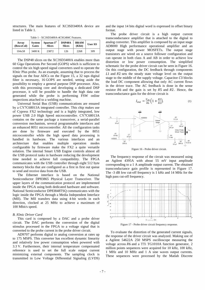
The probe driver circuit is a high output current transconductance amplifier that is attached to the digital to analog converter. This amplifier is composed by an input stage AD8000 High performance operational amplifier and an output stage with power MOSFETs. The output stage transistors are wired on a source follower configuration and can operate in both class A and AB in order to achieve low distortion or low power consumption. The simplified schematic for the probe driver circuit can be seen in Figure 16. On this configuration, the DC feedback through components
and sets the steady state voltage level on the output stage to the middle of the supply voltage. Capacitor blocks the load DC component allowing that only AC current flows in the driver trace. The AC feedback is done in the sense resistor and the gain is set by and . Hence, the transconductance gain for the driver circuit is
. (1)
R30.1 Ω
C3100 µF
R60.22 Ω
+VDD
R2100 Ω
R5300 Ω
C410 µF
R110 kΩ
+VDD/2
C110 µF
Vin +
-
AD8000
C210 µF
Output Stage
IOnic Probe Driver Trace
+VDD
L110 µH
R41 kΩ
Iout
Figure 16 - Probe driver circuit.
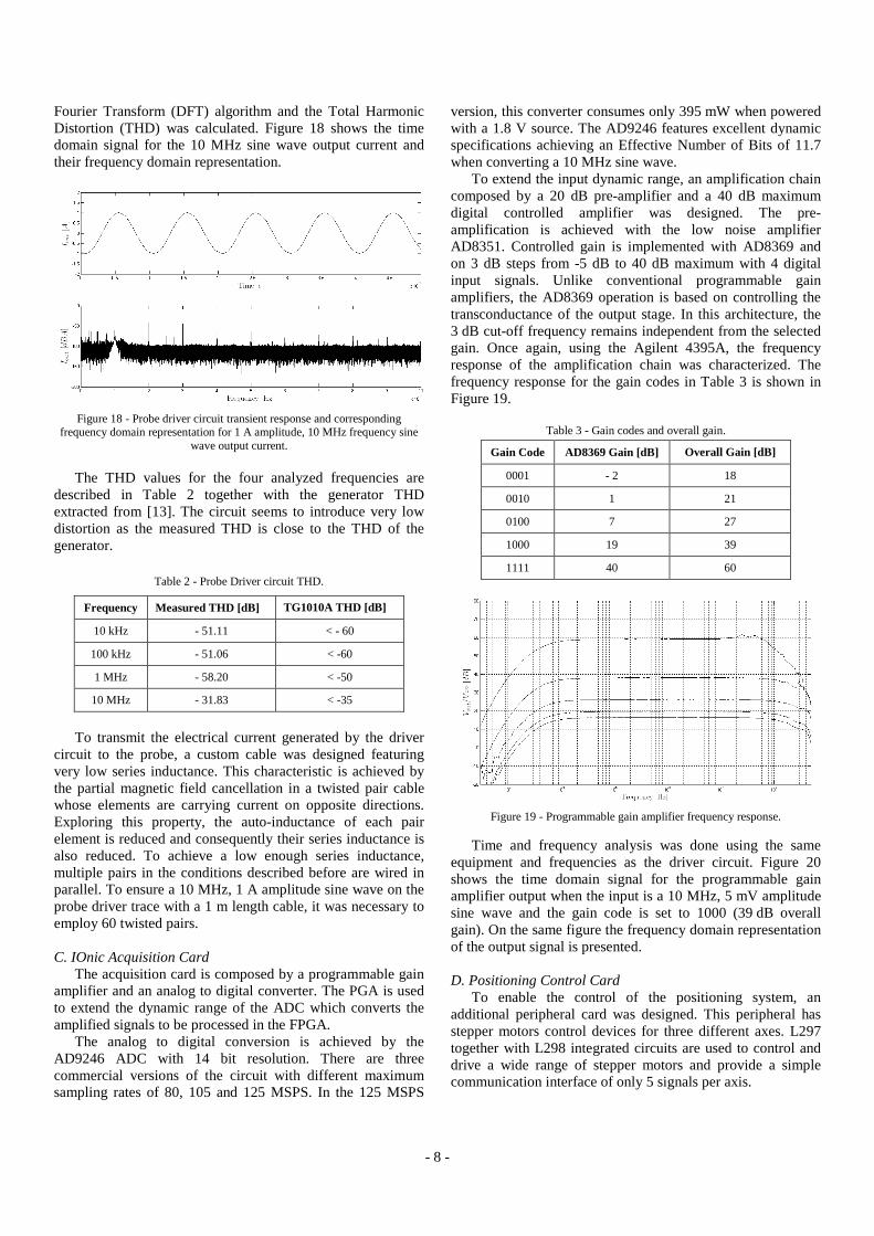
The frequency response of the circuit was measured using
an Agilent 4395A with about 55 mV input amplitude corresponding to a 1 A amplitude output current. The obtained transconductance gain profile is represented in Figure 17. The -3 dB low cut-off frequency is 1 kHz and 14 MHz for the high pass cut-off frequency.
Figure 17 - Probe driver circuit frequency response.
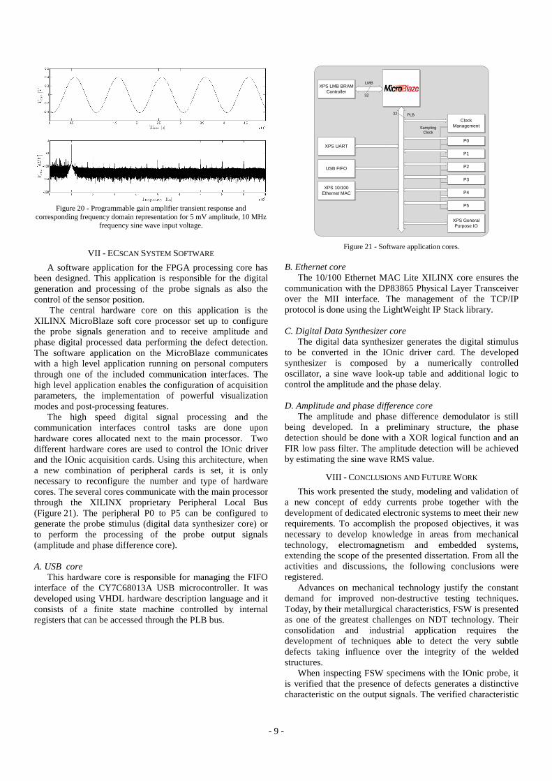
To evaluate the distortion of the generated current signals,
the response of the driver circuit was analyzed. Making use of a Agilent 54622A 250 MSPS oscilloscope measuring the voltage across and a TTi TG1010A function generator, 2 million points sequences were acquired for 10 kHz, 100 kHz, 1 MHz and 10 MHz and 1 A sine waves output currents. These sequences were processed by the Matlab Discrete
- 8 -
Fourier Transform (DFT) algorithm and the Total Harmonic Distortion (THD) was calculated. Figure 18 shows the time domain signal for the 10 MHz sine wave output current and their frequency domain representation.
Figure 18 - Probe driver circuit transient response and corresponding
frequency domain representation for 1 A amplitude, 10 MHz frequency sine wave output current.
The THD values for the four analyzed frequencies are
described in Table 2 together with the generator THD extracted from [13]. The circuit seems to introduce very low distortion as the measured THD is close to the THD of the generator.
Table 2 - Probe Driver circuit THD.
Frequency Measured THD [dB] TG1010A THD [dB]
10 kHz - 51.11 < - 60
100 kHz - 51.06 < -60
1 MHz - 58.20 < -50
10 MHz - 31.83 < -35
To transmit the electrical current generated by the driver
circuit to the probe, a custom cable was designed featuring very low series inductance. This characteristic is achieved by the partial magnetic field cancellation in a twisted pair cable whose elements are carrying current on opposite directions. Exploring this property, the auto-inductance of each pair element is reduced and consequently their series inductance is also reduced. To achieve a low enough series inductance, multiple pairs in the conditions described before are wired in parallel. To ensure a 10 MHz, 1 A amplitude sine wave on the probe driver trace with a 1 m length cable, it was necessary to employ 60 twisted pairs.
C. IOnic Acquisition Card
The acquisition card is composed by a programmable gain amplifier and an analog to digital converter. The PGA is used to extend the dynamic range of the ADC which converts the amplified signals to be processed in the FPGA.
The analog to digital conversion is achieved by the AD9246 ADC with 14 bit resolution. There are three commercial versions of the circuit with different maximum sampling rates of 80, 105 and 125 MSPS. In the 125 MSPS
version, this converter consumes only 395 mW when powered with a 1.8 V source. The AD9246 features excellent dynamic specifications achieving an Effective Number of Bits of 11.7 when converting a 10 MHz sine wave.
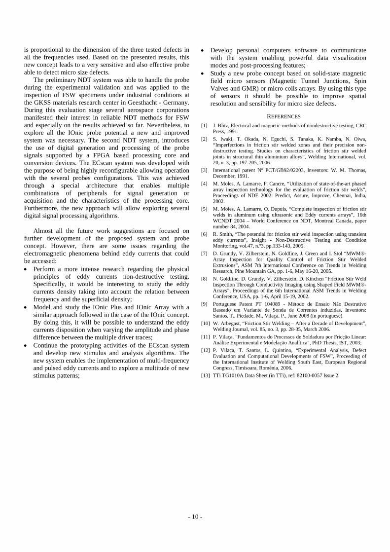
To extend the input dynamic range, an amplification chain composed by a 20 dB pre-amplifier and a 40 dB maximum digital controlled amplifier was designed. The pre-amplification is achieved with the low noise amplifier AD8351. Controlled gain is implemented with AD8369 and on 3 dB steps from -5 dB to 40 dB maximum with 4 digital input signals. Unlike conventional programmable gain amplifiers, the AD8369 operation is based on controlling the transconductance of the output stage. In this architecture, the 3 dB cut-off frequency remains independent from the selected gain. Once again, using the Agilent 4395A, the frequency response of the amplification chain was characterized. The frequency response for the gain codes in Table 3 is shown in Figure 19.
Table 3 - Gain codes and overall gain.
Gain Code AD8369 Gain [dB] Overall Gain [dB]
0001 - 2 18
0010 1 21
0100 7 27
1000 19 39
1111 40 60
Figure 19 - Programmable gain amplifier frequency response.
Time and frequency analysis was done using the same
equipment and frequencies as the driver circuit. Figure 20 shows the time domain signal for the programmable gain amplifier output when the input is a 10 MHz, 5 mV amplitude sine wave and the gain code is set to 1000 (39 dB overall gain). On the same figure the frequency domain representation of the output signal is presented.
D. Positioning Control Card
To enable the control of the positioning system, an additional peripheral card was designed. This peripheral has stepper motors control devices for three different axes. L297 together with L298 integrated circuits are used to control and drive a wide range of stepper motors and provide a simple communication interface of only 5 signals per axis.
- 9 -
Figure 20 - Programmable gain amplifier transient response and
corresponding frequency domain representation for 5 mV amplitude, 10 MHz frequency sine wave input voltage.
VII - ECSCAN SYSTEM SOFTWARE A software application for the FPGA processing core has
been designed. This application is responsible for the digital generation and processing of the probe signals as also the control of the sensor position.
The central hardware core on this application is the XILINX MicroBlaze soft core processor set up to configure the probe signals generation and to receive amplitude and phase digital processed data performing the defect detection. The software application on the MicroBlaze communicates with a high level application running on personal computers through one of the included communication interfaces. The high level application enables the configuration of acquisition parameters, the implementation of powerful visualization modes and post-processing features.
The high speed digital signal processing and the communication interfaces control tasks are done upon hardware cores allocated next to the main processor. Two different hardware cores are used to control the IOnic driver and the IOnic acquisition cards. Using this architecture, when a new combination of peripheral cards is set, it is only necessary to reconfigure the number and type of hardware cores. The several cores communicate with the main processor through the XILINX proprietary Peripheral Local Bus (Figure 21). The peripheral P0 to P5 can be configured to generate the probe stimulus (digital data synthesizer core) or to perform the processing of the probe output signals (amplitude and phase difference core).
A. USB core
This hardware core is responsible for managing the FIFO interface of the CY7C68013A USB microcontroller. It was developed using VHDL hardware description language and it consists of a finite state machine controlled by internal registers that can be accessed through the PLB bus.
XPS 10/100 Ethernet MAC
XPS UART
XPS LMB BRAM Controller
P0
P1
P2
P3
P4
P5
USB FIFO
PLB32
LMB
32
Sampling Clock
XPS General Purpose IO
Clock Management
Figure 21 - Software application cores.
B. Ethernet core
The 10/100 Ethernet MAC Lite XILINX core ensures the communication with the DP83865 Physical Layer Transceiver over the MII interface. The management of the TCP/IP protocol is done using the LightWeight IP Stack library.
C. Digital Data Synthesizer core
The digital data synthesizer generates the digital stimulus to be converted in the IOnic driver card. The developed synthesizer is composed by a numerically controlled oscillator, a sine wave look-up table and additional logic to control the amplitude and the phase delay.
D. Amplitude and phase difference core
The amplitude and phase difference demodulator is still being developed. In a preliminary structure, the phase detection should be done with a XOR logical function and an FIR low pass filter. The amplitude detection will be achieved by estimating the sine wave RMS value.
VIII - CONCLUSIONS AND FUTURE WORK This work presented the study, modeling and validation of
a new concept of eddy currents probe together with the development of dedicated electronic systems to meet their new requirements. To accomplish the proposed objectives, it was necessary to develop knowledge in areas from mechanical technology, electromagnetism and embedded systems, extending the scope of the presented dissertation. From all the activities and discussions, the following conclusions were registered.
Advances on mechanical technology justify the constant demand for improved non-destructive testing techniques. Today, by their metallurgical characteristics, FSW is presented as one of the greatest challenges on NDT technology. Their consolidation and industrial application requires the development of techniques able to detect the very subtle defects taking influence over the integrity of the welded structures.
When inspecting FSW specimens with the IOnic probe, it is verified that the presence of defects generates a distinctive characteristic on the output signals. The verified characteristic
- 10 -
is proportional to the dimension of the three tested defects in all the frequencies used. Based on the presented results, this new concept leads to a very sensitive and also effective probe able to detect micro size defects.
The preliminary NDT system was able to handle the probe during the experimental validation and was applied to the inspection of FSW specimens under industrial conditions at the GKSS materials research center in Geesthacht - Germany. During this evaluation stage several aerospace corporations manifested their interest in reliable NDT methods for FSW and especially on the results achieved so far. Nevertheless, to explore all the IOnic probe potential a new and improved system was necessary. The second NDT system, introduces the use of digital generation and processing of the probe signals supported by a FPGA based processing core and conversion devices. The ECscan system was developed with the purpose of being highly reconfigurable allowing operation with the several probes configurations. This was achieved through a special architecture that enables multiple combinations of peripherals for signal generation or acquisition and the characteristics of the processing core. Furthermore, the new approach will allow exploring several digital signal processing algorithms.
Almost all the future work suggestions are focused on
further development of the proposed system and probe concept. However, there are some issues regarding the electromagnetic phenomena behind eddy currents that could be accessed: • Perform a more intense research regarding the physical
principles of eddy currents non-destructive testing. Specifically, it would be interesting to study the eddy currents density taking into account the relation between frequency and the superficial density;
• Model and study the IOnic Plus and IOnic Array with a similar approach followed in the case of the IOnic concept. By doing this, it will be possible to understand the eddy currents disposition when varying the amplitude and phase difference between the multiple driver traces;
• Continue the prototyping activities of the ECscan system and develop new stimulus and analysis algorithms. The new system enables the implementation of multi-frequency and pulsed eddy currents and to explore a multitude of new stimulus patterns;
• Develop personal computers software to communicate with the system enabling powerful data visualization modes and post-processing features;
• Study a new probe concept based on solid-state magnetic field micro sensors (Magnetic Tunnel Junctions, Spin Valves and GMR) or micro coils arrays. By using this type of sensors it should be possible to improve spatial resolution and sensibility for micro size defects.
REFERENCES [1] J. Blitz, Electrical and magnetic methods of nondestructive testing, CRC
Press, 1991. [2] S. Iwaki, T. Okada, N. Eguchi, S. Tanaka, K. Namba, N. Oiwa,
“Imperfections in friction stir welded zones and their precision non-destructive testing. Studies on characteristics of friction stir welded joints in structural thin aluminium alloys”, Welding International, vol. 20, n. 3, pp. 197-205, 2006.
[3] International patent Nº PCT/GB92/02203, Inventors: W. M. Thomas, December, 1991.
[4] M. Moles, A. Lamarre, F. Cancre, “Utilization of state-of-the-art phased array inspection technology for the evaluation of friction stir welds”, Proceedings of NDE 2002: Predict, Assure, Improve, Chennai, India, 2002.
[5] M. Moles, A. Lamarre, O. Dupuis, “Complete inspection of friction stir welds in aluminum using ultrasonic and Eddy currents arrays”, 16th WCNDT 2004 – World Conference on NDT, Montreal Canada, paper number 84, 2004.
[6] R. Smith, “The potential for friction stir weld inspection using transient eddy currents”, Insight - Non-Destructive Testing and Condition Monitoring, vol.47, n.º3, pp.133-143, 2005.
[7] D. Grundy, V. Zilberstein, N. Goldfine, J. Green and I. Stol “MWM®-Array Inspection for Quality Control of Friction Stir Welded Extrusions”, ASM 7th International Conference on Trends in Welding Research, Pine Mountain GA, pp. 1-6, May 16-20, 2005.
[8] N. Goldfine, D. Grundy, V. Zilberstein, D. Kinchen “Friction Stir Weld Inspection Through Conductivity Imaging using Shaped Field MWM®-Arrays”, Proceedings of the 6th International ASM Trends in Welding Conference, USA, pp. 1-6, April 15-19, 2002.
[9] Portuguese Patent PT 104089 - Método de Ensaio Não Destrutivo Baseado em Variante de Sonda de Correntes induzidas, Inventors: Santos, T., Piedade, M., Vilaça, P., June 2008 (in portuguese).
[10] W. Arbegast, “Friction Stir Welding – After a Decade of Development”, Welding Journal, vol. 85, no. 3, pp. 28-35, March 2006.
[11] P. Vilaça, "Fundamentos do Processos de Soldadura por Fricção Linear: Análise Experimental e Modelação Analítica", PhD Thesis, IST, 2003;
[12] P. Vilaça, T. Santos, L. Quintino, “Experimental Analysis, Defect Evaluation and Computational Developments of FSW”, Proceeding of the International Institute of Welding South East, European Regional Congress, Timisoara, Roménia, 2006.
[13] TTi TG1010A Data Sheet (in TTi), ref: 82100-0057 Issue 2.