Nonlinear DC equivalent circuits for ferroelectric memristor and Its FSM application P. Michael Preetam Raj a , Amlan Ranjan Kalita a , Mantu K. Hudait b , Shashank Priya c , and Souvik Kundu a a Department of Electrical and Electronics Engineering, Birla Institute of Technology & Science (BITS) Pilani, Hyderabad Campus, Hyderabad, India; b Department of Electrical Engineering and Computer Science, Virginia Tech, Blacksburg, Virginia, USA; c Department of Mechanical Engineering, CEHMS, Virginia Tech, Blacksburg, Virginia, USA ABSTRACT Pt/BaTiO 3 -BiFeO 3 /Nb:SrTiO 3 based memristors were fabricated and their current–voltage (I–V) characteristics were studied in order to facilitate integration with analog/digital computations. Piecewise non-linear I–V characteristic equations of the ferroelectric memristor were obtained using non-linear regression techniques. An equivalent circuit for the fabricated memristors was obtained comprising of internal current, film resistance, and voltage dependent resistance. Utilizing the equivalent circuit model, a three bit general purpose Finite State Machine was developed and simulated results were found to match with the fabricated FSM device results. ARTICLE HISTORY Received 1 April 2018 Accepted 30 August 2018 KEYWORDS Band alignment; finite state machine; polarization inversion; resist- ive switching 1. Introduction Memristor was theoretically predicted to be fundamental component correlating flux-linkage and charge [1]. Later, it was identified that both solid-state electronic and ionic transport were responsible for observance of memristance. Memristive behaviour has been modeled by hyperbolic and exponential functions to provide representation for current–voltage (I–V) relation [2]. However, these functions are complex and require simplification for facilitating the circuit design. Several efforts have been made in order to construct an accurate mathematical model of a memristor. A cubic polyno- mial expression was predicted to represent relationship between the flux-linkage and charge [2–5]. Single approximate mathematical model of the prototype memristor has also been proposed using SPICE model [6]. Lehtonen et al. have studied the memristor based cellular non-linear networks (CNN) and described that the state variable of mem- ristance is related to applied voltage through a polynomial function [7]. However, a comprehensive model that can directly correlate memristive I-V behaviour through sim- plified mathematical function is needed. Recently, a memristor crossbar circuit was designed based upon quantum mechanical tunnelling phenomenon [8]. This structure requires several computations in solving state equations. Memristive functions were identified to be nonlinear and different methods were proposed for their compensation CONTACT Souvik Kundu [email protected]Color versions of one or more of the figures in the article can be found online at www.tandfonline.com/ginf. ß 2018 Taylor & Francis Group, LLC INTEGRATED FERROELECTRICS 2018, VOL. 192, 16–27 https://doi.org/10.1080/10584587.2018.1521667
Transcript
Nonlinear DC equivalent circuits for ferroelectric memristorand Its FSM application
P. Michael Preetam Raja, Amlan Ranjan Kalitaa, Mantu K. Hudaitb, Shashank Priyac,and Souvik Kundua
aDepartment of Electrical and Electronics Engineering, Birla Institute of Technology & Science (BITS)Pilani, Hyderabad Campus, Hyderabad, India; bDepartment of Electrical Engineering and ComputerScience, Virginia Tech, Blacksburg, Virginia, USA; cDepartment of Mechanical Engineering, CEHMS,Virginia Tech, Blacksburg, Virginia, USA
ABSTRACTPt/BaTiO3-BiFeO3/Nb:SrTiO3 based memristors were fabricated andtheir current–voltage (I–V) characteristics were studied in order tofacilitate integration with analog/digital computations. Piecewisenon-linear I–V characteristic equations of the ferroelectric memristorwere obtained using non-linear regression techniques. An equivalentcircuit for the fabricated memristors was obtained comprising ofinternal current, film resistance, and voltage dependent resistance.Utilizing the equivalent circuit model, a three bit general purposeFinite State Machine was developed and simulated results werefound to match with the fabricated FSM device results.
ARTICLE HISTORYReceived 1 April 2018Accepted 30 August 2018
Memristor was theoretically predicted to be fundamental component correlatingflux-linkage and charge [1]. Later, it was identified that both solid-state electronic andionic transport were responsible for observance of memristance. Memristive behaviourhas been modeled by hyperbolic and exponential functions to provide representationfor current–voltage (I–V) relation [2]. However, these functions are complex andrequire simplification for facilitating the circuit design. Several efforts have been madein order to construct an accurate mathematical model of a memristor. A cubic polyno-mial expression was predicted to represent relationship between the flux-linkage andcharge [2–5]. Single approximate mathematical model of the prototype memristor hasalso been proposed using SPICE model [6]. Lehtonen et al. have studied the memristorbased cellular non-linear networks (CNN) and described that the state variable of mem-ristance is related to applied voltage through a polynomial function [7]. However, acomprehensive model that can directly correlate memristive I-V behaviour through sim-plified mathematical function is needed. Recently, a memristor crossbar circuit wasdesigned based upon quantum mechanical tunnelling phenomenon [8]. This structurerequires several computations in solving state equations. Memristive functions wereidentified to be nonlinear and different methods were proposed for their compensation
CONTACT Souvik Kundu [email protected] versions of one or more of the figures in the article can be found online at www.tandfonline.com/ginf.� 2018 Taylor & Francis Group, LLC
[9]. Knag et al. first utilized methods such as voltage predistortion, parallel single-pulsewrite, and downscaled write and up scaled read, and then invoked linear models [9].Being a two-step process, this adds up to the computational complexity. A single non-linear model based upon I-V characteristics is preferred.In our prior work, we have demonstrated lead-free ferroelectric based Pt/BaTiO3-
BiFeO3 (BT-BFO)/Nb:SrTiO3 memristor and our investigations have shown excellentwrite-read memory properties by invoking polarization inversion [10]. This break-through was possible due to the development of a new class of ferroelectric materialexhiting poalrization switching in nanoscale thin films and its successful integrationwith Nb-doped SrTiO3 substrate. We have also demonstrated that the fabricated deviceshad excellent retention and switching capabilities. Building upon this prior work, wehave fabricated Pt/BT-BFO/Nb:STO memristor devices and analysed piecewise non-linear I–V characteristic equations to develop its equivalent circuit model. Two-levelmemristive logic has been shown to provide better noise margin since the operationalfrequency of memristor based logic has inconsistency in switching between SET andRESET states [11]. Hence, the goal in this study is on developing a two-level BT-BFOmemristive logic model with higher accuracy and low computational complexities andvalidating the correspondence between the real BT-BFO memristor and its proposedequivalent circuit.For facilitating the application in analog or digital computation, we have developed
alternative Finite State Machines (FSMs). FSMs were usually built using different logicgates and flip-flops, which require a large number of transistors [12–14]. However, con-ventional transistor based FSMs are not suitable for low-power, high-speed and minia-turized systems [15]. Moreover, transistor based FSMs require additional circuitry astransistors are not natural state programmable devices. On the other hand, memristorsare natural resistive state changing elements and could be used to develop such FSMswhile providing other advantages such as low-power consumption, non-volatility, lowercomplex architecture, high packing density (46% of area reduction as compared toSRAM) and most importantly easy fabrication steps [16–20]. Therefore, in this work,we have focused our efforts to demonstrate BT-BFO memristor based FSMs to over-come the above mentioned problems associated with conventional transistor devices.
2. Experimental work
BT-BFO based memristor devices were fabricated on Nb:STO (Nb 0.7wt%) substrates,where Nb:STO was used as bottom electrode and Pt served as top electrode. All the fab-rication steps are described elsewhere [10]. Keithley 4200-SCS was used to measure theI�V characteristics of fabricated memristors. Multisim 13.0 (National Instrument) wasused to simulate the equivalent circuits based on memristor.
3. Results and discussion
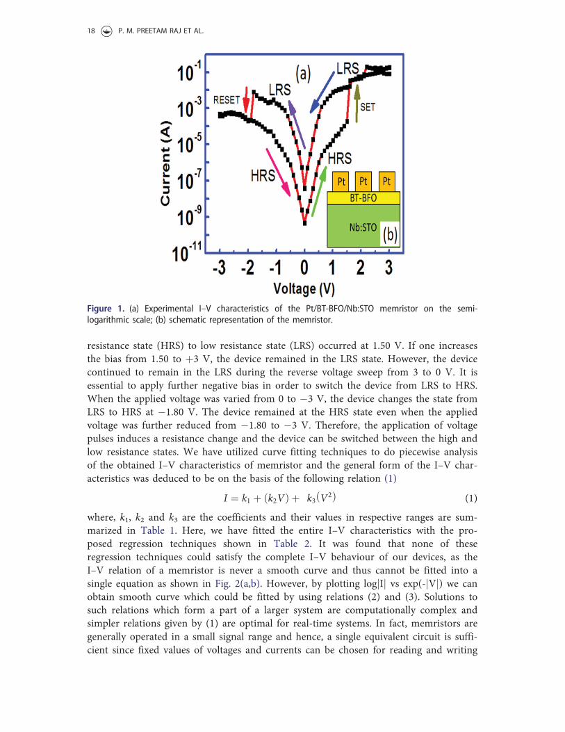
The I-V characteristics of fabricated Pt/BT-BFO/Nb:STO memristors were measured bysweeping the voltage from 0 to þ3 V,þ 3 to 0 V, 0 to �3 V and �3 to 0 V, as shownin Fig. 1(a). From the I–V characteristics, it was found that the transition from high
INTEGRATED FERROELECTRICS 17
resistance state (HRS) to low resistance state (LRS) occurred at 1.50 V. If one increasesthe bias from 1.50 to þ3 V, the device remained in the LRS state. However, the devicecontinued to remain in the LRS during the reverse voltage sweep from 3 to 0 V. It isessential to apply further negative bias in order to switch the device from LRS to HRS.When the applied voltage was varied from 0 to �3 V, the device changes the state fromLRS to HRS at �1.80 V. The device remained at the HRS state even when the appliedvoltage was further reduced from �1.80 to �3 V. Therefore, the application of voltagepulses induces a resistance change and the device can be switched between the high andlow resistance states. We have utilized curve fitting techniques to do piecewise analysisof the obtained I–V characteristics of memristor and the general form of the I–V char-acteristics was deduced to be on the basis of the following relation (1)
I ¼ k1 þ k2Vð Þ þ k3 V2ð Þ� �(1)
where, k1, k2 and k3 are the coefficients and their values in respective ranges are sum-marized in Table 1. Here, we have fitted the entire I–V characteristics with the pro-posed regression techniques shown in Table 2. It was found that none of theseregression techniques could satisfy the complete I–V behaviour of our devices, as theI–V relation of a memristor is never a smooth curve and thus cannot be fitted into asingle equation as shown in Fig. 2(a,b). However, by plotting logjIj vs exp(-jVj) we canobtain smooth curve which could be fitted by using relations (2) and (3). Solutions tosuch relations which form a part of a larger system are computationally complex andsimpler relations given by (1) are optimal for real-time systems. In fact, memristors aregenerally operated in a small signal range and hence, a single equivalent circuit is suffi-cient since fixed values of voltages and currents can be chosen for reading and writing
Figure 1. (a) Experimental I–V characteristics of the Pt/BT-BFO/Nb:STO memristor on the semi-logarithmic scale; (b) schematic representation of the memristor.
18 P. M. PREETAM RAJ ET AL.
Table 1. Obtained parameters for memristor through curve fitting.
Applied voltage range Resistive state k1 k2 k3�3V to �1.9V High �0.004237025 �0.003652722 �6.9847E� 4�1.79987V to (4.92E� 05)V Low 1.826305E� 4 0.0012584036 0.0026185849(4.92E� 05)V to 1.59995 V Low �5.6196624E� 4 �2.12205E� 5 0.00738861261.70012V to 2.70027V Low �0.0422095 0.031246 0.008689382.80039V to 3.00397V Low 4.48 �2.98 0.5043V to 2.2V Low 1.23349 �0.8071 0.1523462.1V to 1.6V Low 0.28833 �0.34185 0.1144621.5V to 1.2V High 0.0019042 �0.0031996 0.001273361.1V to 0.8V High 1.96492E� 4 �4.6351E� 4 2.84678E� 40.7V to 0V High 3.2186662E� 7 �7.0693112E� 6 1.844603E� 5(4.92E� 05) V to �2.6V High �2.8911612E� 5 1.5686767E� 4 1.4022803E� 4�2.7V to �3V High �0.007231 �0.006067 �0.001175
Table 2. Different regression techniques used.
Technique Equation
Linear I ¼ k1 þ ðk2VÞe-Exponential I ¼ k1eðk2VÞab-Exponential I ¼ k1ðk2VÞPower I ¼ k1ðVk2 ÞInverse I ¼ k1 þ ðk2=VÞQuadratic I ¼ k1 þ ðk2VÞ þ ðk3ðV2ÞÞLogarithmic I ¼ k1 þ ðk2 lnðVÞÞ
Figure 2. (a) Fitting of I–V curve high resistive hysteresis values; (b) for low resistive hysteresis values;(c) logjIj versus exp(-jVj) during high to low switching; and (d) during low to high switching.
INTEGRATED FERROELECTRICS 19
data to a memristor. Piecewise curve fitting was invoked, where a range of continuousappearing I–V characteristic readings were fitted with the relations shown in Table 2.Interestingly, it was found that the best fit, in all the cases was possible only with thequadratic regression technique as shown in Fig. 3 to Fig. 5. The analysis based uponthese figures demonstrates that relation (1) has a good match in all the cases, where thesolid curve represents the plot of the relation while experimental results are representedby red dotted points. Moreover, when fitting was done for logjIj vs V (Fig. 6) plot,smooth curves (R2 values ranging from 0.98 to 0.99, which is close to ideal value 1)were obtained as compared to the earlier cases, which shows that relation (4) providesbetter representation. The obtained curves of exp(-jVj) vs logjIj (shown in Fig. 2) and Vvs log(I) (shown in Fig. 6) represent the resistive switching instance from low to highand vice versa, with better accuracy (with high R2 values ranging from 0.98 to 0.99).The curve fitting resulted in perplexed relations, thus, the piecewise second order poly-nomial relation (1) is found to be optimal in terms of both accuracy and computationalcomplexities. One could also choose hyperbolic and exponential relations with higherorder polynomials though it will reduce computational ease. As seen from relation (1),a second order polynomial directly relating I and V is much simpler to use as comparedto other relations; therefore, the DC equivalent circuit model was developed utilizing
Figure 3. Piecewise curve fitting of the I–V relation for the range of (a)� 3V to �1.9V; (b)� 1.80 Vto (4.92E� 05)V; (c) (4.92E� 05)V to 1.60 V; and (d) 1.70 V to 2.70 V.
20 P. M. PREETAM RAJ ET AL.
relation (1) as shown in Fig. 7. Our analysis showed that the equivalent circuit consistsof a voltage dependent resistor (1/Vk3). In addition, the equivalent circuit also com-prises of voltage independent current source (k1) and film resistances (1/k2) whichcould further be modelled using programmed circuit elements. In our analysis, the cur-rent source is due to the polarization effects in memristor. In order to verify the pro-posed model, a voltage source ‘V’ is connected at the input of the proposed circuitshown in Fig. 7, where k1, k2 and k3 are dependent on the range of applied voltages asshown in Table 1. This arrangement was made to identify the current through thememristor equivalent circuit for an applied input voltage. During LRS, when 1 V wasapplied at the input, the obtained simulated LRS current was found to be 6.86mA,which changed to 55.08mA when the applied voltage was 2 V. These values are wellmatched with the experimental results where the LRS current was found to be 7.87mAand 58.62mA for an applied voltage of 1 V and 2 V, respectively. Similar study wasmade during HRS, though the currents were found to be very low, as the device is inthe off state. These results validate the equivalent circuit proposed for ferroelectric oxidebased memristor. It is important to mention that the parameters such as polarizationdependent current source, film resistance, and voltage dependent resistance will bechanged for different dimensions or architectures of memristors. In our case, the devicehas 50 nm thin BT-BFO film on Nb:STO substrate and 80 nm top Pt electrodes of
Figure 4. Piecewise curve fitting of the I–V relation for the range of (a) 2.80V to 3.00 V; (b)(4.92E� 05) V to �2.6; (c)� 2.70 V to �3.00 V; and (d) 3.00 V to 2.20 V.
INTEGRATED FERROELECTRICS 21
dimension 600 lm� 600lm separated by 200lm. The change in parametric values withdifferent dimensions are mainly due to the variation of the resistive switching voltageand current values that are dependent on polarization, film resistances and memristiveproperties, which in turn are dependent upon the materials used and their dimensions.During the resistive switching HRS to LRS from 0 to 3V, the best single fit to representthe I–V behaviour of our memristor can be given by the relation (2).
e �jVjð Þ ¼ �4:00505�17:3958289= log jIj� �(2)
For resistive switching LRS to HRS from 0 to �3 V the best single fit relation to rep-resent the I–V behaviour of memristor can be given by the relation (3).
The best single fit relation for resistive switching HRS to LRS from 0 to 3V relatinglogjIj and V can be given by the relation (4).
log jIj� � ¼ �6:1221þ 4:70876V�1:05786V2 (4)
Memristor with changeable resistive states can be a potential candidate for FSMs.Traditionally, transistors have been used for designing FSMs which is becoming
Figure 5. Piecewise curve fitting of the I–V relation for the range of (a) 2.10 V to 1.60 V; (b) 1.50 Vto 1.20 V; (c) 1.10 V to 0.80 V; and (d) 0.70 V to 0V.
22 P. M. PREETAM RAJ ET AL.
challenging [21–23]. The state of the transistors never gets changed, therefore, severalcombinations of circuit elements are necessary for designing transistor coupled FSMs.Here, we provide demonstration of a novel three bit FSM with 8 discrete voltage levelsusing memristors and develop the corresponding equivalent circuits, as shown in Fig.8(a) (for (000) state) and Fig. 8(b) (for (111) state). We have considered all the resist-ance/voltage values up to two digits after decimal, otherwise it is practically impossibleto precisely obtain more digits after decimal using common oscilloscope or multimeters. For the (000) state, the circuit shown in Fig. 8(a) was simulated and the corre-sponding output voltage magnitude was found to be 3.03 V. On the other side, themagnitude of output voltage for the (111) state was found to be 4.92 V. For the otherstates in between (000) to (111), the voltage levels will lie in the range of 3.03 V to 4.92V. In comparison, for the transistor coupled FSMs, the circuit consists of several tran-sistors for implementing the same 3 bit FSM [12–14]. It is essential to mention herethat higher number of transistors is required when the number of state transitions aswell as the number of bits of an FSM is increased. Interestingly, only n numbers ofmemristors are required for an n-bit FSM, irrespective of the number of statetransitions.
Figure 6. Piecewise curve fitting of log (current) versus voltage relation for the range of (a) 0 to 3.00V; (b) 0 to �3.00 V; (c) 1.50 to 0 V; and (d)� 1.50 V to 0 V.
INTEGRATED FERROELECTRICS 23
Thus, the proposed FSM model is far superior as the state changes between any ofthe 8 states is possible with minimum number of circuit elements as discussed. In orderto validate the equivalent circuits and simulated FSM results, similar experiments were
Figure 7. Schematic of (a) sample LRS equivalent circuit at 1 V and (b) equivalent circuit at 2V.
Figure 8. Memristive 3 bit general purpose FSM for (a) (000) state and (b) (111) state.
24 P. M. PREETAM RAJ ET AL.
performed using the fabricated BT-BFO based memristors. For the equivalent circuit, ageneral form of the circuit was developed (shown in Fig. 9(a)) from Fig. 7, where k1, k2and k3 values depend on the range of applied voltages as tabulated in Table 1. ForFSMs, the general form of Fig. 8(a,b) can be seen in Fig. 9(b). In order to prevent thedamage of BT-BFO based memristors, a series resistance of 100 X was connectedbetween the source and memristors (IC 741 was used as operational amplifier). For the(000) state, the output voltage was recorded to be 3.05 V; whereas for (111) state, it was4.90 V. These results matched well with the simulated case and corraborate the effect-iveness of our proposed circuits in order to provide alternative for conventional transis-tors coupled FSMs. Also, in order to change or program the memristive states, a pulsevoltage of height þ1.50 V and �1.80 V can be applied for LRS and HRS, respectively.It is extremely important to mention that the applied voltages 0.30 V (LSB), 0.60 V and1.20 V (MSB) are in the ratio 1:2:4 (as shown in Figs.8 and9). These voltages are usedas the necessary multiplying factors to generate the decimal equivalent voltages corre-sponding to the 3-bit binary logic states. The Op-amp and variable resistor R are usedfor isolation and adjusting the output voltage levels. The values of k1, k2 and k3 can bechosen from Table 1.
4. Summary
I–V relations were developed for Pt/BT-BFO/Nb:STO memristor using curve-fittingtechniques. Piece-wise DC equivalent circuits were constructed from these relations. It
Figure 9. General structure of (a) proposed equivalent circuit of memristor and (b) memristive3 bit FSM.
INTEGRATED FERROELECTRICS 25
is found that piece-wise memristive I–V relations are optimally represented by secondorder polynomial relations and thus a single DC equivalent circuit for a memristor, forall cases, is constructed using programmable current source, film resistance and voltagevarying resistances. Also it is found that during the resistive switching, the I–V behav-iour follows logarithmic and exponential relations, respectively. These results are usefulto construct application oriented optimal software models for memristors. A novel 3 bitgeneral purpose FSM using the proposed memristive equivalent circuits was modelledand the results were compared with the fabricated one. Both the results were wellmatched and the proposed design offers its potential use in futuristic FSM, an alterna-tive choice to the use of transistor which ultimately reduces the circuit complexity.
References
1. L. O. Chua, Memristor - the missing circuit element, IEEE Trans. Circuit Theory. CT-18(5), 507–519 (1971).
2. D. B. Strukov et al., The missing memristor found, Nat. Lett. 453(7191), 80–83 (2008).3. L. O. Chua, Resistance switching memories are memristors, Appl. Phys. A. 102(4), 765–783
(2011).4. F. Corinto and A. Ascoli, A boundary condition-based approach to the modeling of mem-
ristor nanostructures, IEEE Trans. Circuits Syst. 59(11), 2713–2726 (2012).5. O. Kavehei et al., The fourth element: characteristics, modelling and electromagnetic theory
of the Memristor, Proc. Math. Phys. Eng. Sci. 466(2120), 2175–2202 (2010).6. Z. Biolek, D. Biolek, and V. Biolkov�a, Spice model of memristor with nonlinear dopant
drift, Radioengineering. 18(2), 210–214 (2009).7. E. Lehtonen and M. Laiho, CNN Using Memristors for Neighborhood Connections, IEEE
CNNA, 12th International Workshop, 2010, doi:10.1109/CNNA.2010.5430304.8. I. Vourkas and G. C. Sirakoulis. A novel design and modeling paradigm for memristor-
based crossbar circuits, IEEE Trans. Nanotechnol. 11(6), 1151–1159 (2012).9. P. Knag, W. Lu, and Z. Zhang, A native stochastic computing architecture enabled by
memristors, IEEE Trans. Nanotechnol. 13(2), 283–293 (2014).10. S. Kundu et al., Lead-free epitaxial ferroelectric material integration on semiconducting
(100) Nb-doped SrTiO3 for low-power non-volatile memory and efficient ultraviolet raydetection, Sci. Rep. 5, 12415 (2015).
11. K. M. Lee et al., The c-Fe2O3 nanoparticle assembly-based memristor ratioed logic and itsoptical tuning, IEEE Electron Device Lett. 37(8), 986–989 (2016).
12. G. De Micheli, R.K. Brayton, and A. Sangiovanni-Vincentelli, Optimal state assignment forfinite state machines, IEEE Trans. Comput. Aided Design Integr. Circuits Syst. 4(3), 269–285(1985).
13. S. Devadas et al., MUSTANG: state assignment of finite state machines targeting multilevellogic implementations, IEEE Trans. Comput.-Aided Design Integr. Circuits Syst. 7(12),1290–1300 (1988).
14. K. Roy and S. Prasad, SYCLOP: synthesis of CMOS logic for low power applications,Computer Design: VLSI in Computers and Processors, ICCD 92, Oct. 1992, doi:10.1109/ICCD.1992.276316.
15. R.S. Williams, How we found the missing memristor, in Memristors Memristive Systems,(Springer, New York, 2014), pp. 3–16.
16. B. Muthuswamy and P. Kokate, Memristor-based chaotic circuits, IETE Tech. Rev. 26(6),417 (2009).
17. K.-H. Jo et al., Self-adaptive write circuit for low-power and variation-tolerant memristors,IEEE Trans. Nanotechnol. 9(6), 675–678 (2010).
26 P. M. PREETAM RAJ ET AL.
18. P.F. Chiu et al., Low store energy, low VDDmin, 8T2R nonvolatile latch and SRAM withvertical-stacked resistive memory (memristor) devices for low power mobile applications,IEEE J. Solid-State Circuits 47(6), 1483–1496 (2012).
19. M. A. Zidan et al., Memristor-based memory: the sneak paths problem and solutions,Microelectronics J. 44(2), 176–183 (2013).
20. K. Eshraghian et al., Memristor MOS content addressable memory (MCAM): hybrid archi-tecture for future high performance search engines, IEEE Trans. Very Large Scale Integr.Syst. 19(8), 1407–1417 (2011).
21. D. Drusinsky and D. Harel, Using statecharts for hardware description and synthesis, IEEETrans. Comput. Des. Integr. Circuits Syst. 8(7), 798–807 (1989).
22. M. A. Pasha, S. Derrien, and O. Sentieys, Ultra low-power FSM for control oriented appli-cations, IEEE International Symposium on Circuits and Systems, pp. 1577–1580 (2009).
23. J. Yao et al., Nanowire nanocomputer as a finite-state machine, Proc. Natl. Acad. Sci. USA.111(7), 2431–2435 (2014).


![FERROELECTRIC RAM [FRAM]](https://static.documents.pub/doc/80x56/56816799550346895ddcd567/ferroelectric-ram-fram.jpg)

![Sangeetha [Ferroelectric Memory]](https://static.documents.pub/doc/80x56/55cf8f91550346703b9d9665/sangeetha-ferroelectric-memory.jpg)


