NOR FLASH MEMORY K8D3x16UTC / K8D3x16UBC Revision 1.7 September, 2006 1 Document Title 32M Bit (4M x8/2M x16) Dual Bank NOR Flash Memory Revision History Revision No. 0.0 1.0 1.1 1.2 1.3 1.4 1.5 1.6 1.7 Remark Preliminary Final History Initial Draft Final Specification Not support 48TSOP1 Package Not support 16M/16M BANK partition Support 48TSOP1 Package Support 48TSOP1 Lead Free Package Support 48FBGA Leaded/Lead Free Package Complement status flag check algorithm tCS timing is modified "Asynchronous mode may not support read following four sequential invalid read condition within 200ns." is added Draft Date June 18, 2002 November 13, 2002 November 18, 2003 July 16, 2004 September 16, 2004 March 16, 2005 June 2, 2005 August 25,2006 September 7, 2006
Transcript
NOR FLASH MEMORYK8D3x16UTC / K8D3x16UBC
Revision 1.7September, 2006
1
Document Title32M Bit (4M x8/2M x16) Dual Bank NOR Flash Memory
Revision HistoryRevision No.
0.0
1.0
1.1
1.2
1.3
1.4
1.5
1.6
1.7
Remark
Preliminary
Final
History
Initial Draft
Final Specification
Not support 48TSOP1 PackageNot support 16M/16M BANK partition
Support 48TSOP1 Package
Support 48TSOP1 Lead Free Package
Support 48FBGA Leaded/Lead Free Package
Complement status flag check algorithm
tCS timing is modified
"Asynchronous mode may not support read following four sequential invalid read condition within 200ns." is added
Draft Date
June 18, 2002
November 13, 2002
November 18, 2003
July 16, 2004
September 16, 2004March 16, 2005
June 2, 2005
August 25,2006
September 7, 2006
NOR FLASH MEMORYK8D3x16UTC / K8D3x16UBC
Revision 1.7September, 2006
2
32M Bit (4M x8/2M x16) Dual Bank NOR Flash Memory
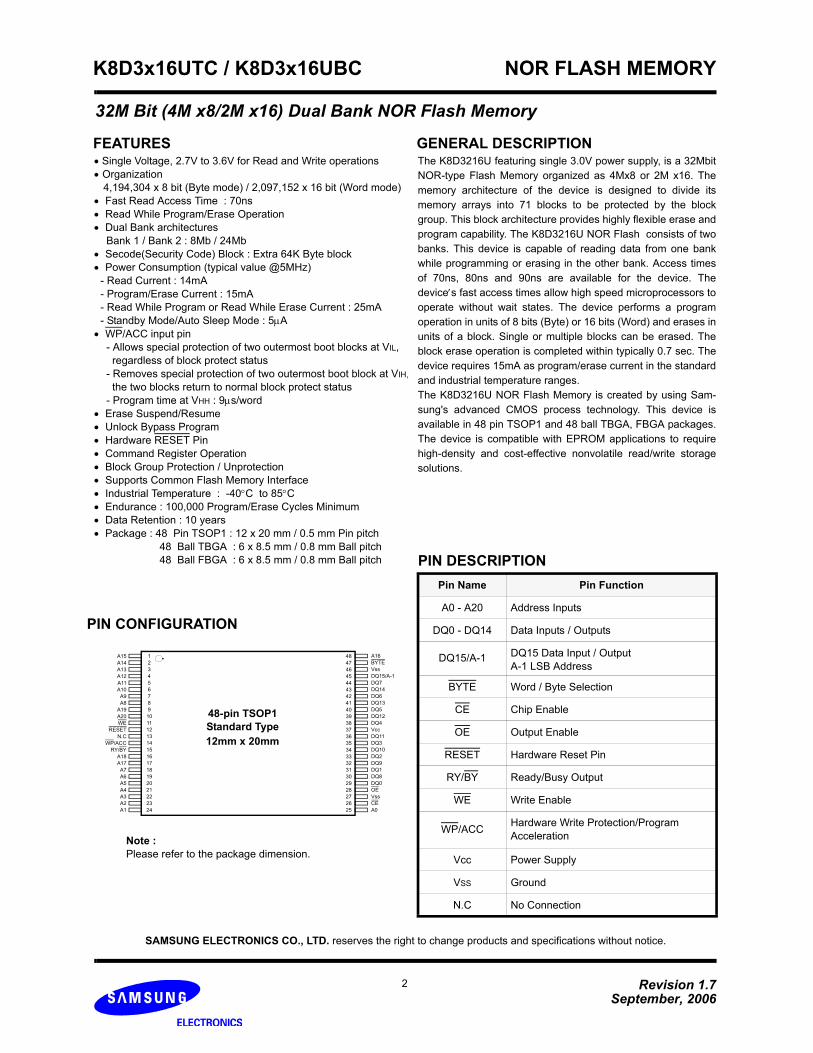
The K8D3216U featuring single 3.0V power supply, is a 32MbitNOR-type Flash Memory organized as 4Mx8 or 2M x16. Thememory architecture of the device is designed to divide itsmemory arrays into 71 blocks to be protected by the blockgroup. This block architecture provides highly flexible erase andprogram capability. The K8D3216U NOR Flash consists of twobanks. This device is capable of reading data from one bankwhile programming or erasing in the other bank. Access timesof 70ns, 80ns and 90ns are available for the device. Thedevice′s fast access times allow high speed microprocessors tooperate without wait states. The device performs a programoperation in units of 8 bits (Byte) or 16 bits (Word) and erases inunits of a block. Single or multiple blocks can be erased. Theblock erase operation is completed within typically 0.7 sec. Thedevice requires 15mA as program/erase current in the standardand industrial temperature ranges. The K8D3216U NOR Flash Memory is created by using Sam-sung's advanced CMOS process technology. This device isavailable in 48 pin TSOP1 and 48 ball TBGA, FBGA packages.The device is compatible with EPROM applications to requirehigh-density and cost-effective nonvolatile read/write storagesolutions.
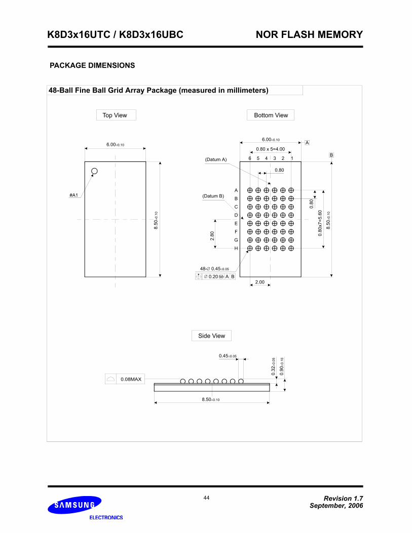
FEATURES• Single Voltage, 2.7V to 3.6V for Read and Write operations• Organization 4,194,304 x 8 bit (Byte mode) / 2,097,152 x 16 bit (Word mode)• Fast Read Access Time : 70ns• Read While Program/Erase Operation• Dual Bank architectures Bank 1 / Bank 2 : 8Mb / 24Mb• Secode(Security Code) Block : Extra 64K Byte block • Power Consumption (typical value @5MHz) - Read Current : 14mA - Program/Erase Current : 15mA - Read While Program or Read While Erase Current : 25mA - Standby Mode/Auto Sleep Mode : 5µA • WP/ACC input pin - Allows special protection of two outermost boot blocks at VIL, regardless of block protect status - Removes special protection of two outermost boot block at VIH, the two blocks return to normal block protect status - Program time at VHH : 9µs/word• Erase Suspend/Resume • Unlock Bypass Program • Hardware RESET Pin• Command Register Operation• Block Group Protection / Unprotection• Supports Common Flash Memory Interface• Industrial Temperature : -40°C to 85°C• Endurance : 100,000 Program/Erase Cycles Minimum• Data Retention : 10 years• Package : 48 Pin TSOP1 : 12 x 20 mm / 0.5 mm Pin pitch 48 Ball TBGA : 6 x 8.5 mm / 0.8 mm Ball pitch 48 Ball FBGA : 6 x 8.5 mm / 0.8 mm Ball pitch
GENERAL DESCRIPTION
SAMSUNG ELECTRONICS CO., LTD. reserves the right to change products and specifications without notice.
BA62 1 1 1 1 1 0 X X X 64/32 3E0000H-3EFFFFH 1F0000H-1F7FFFH
BA61 1 1 1 1 0 1 X X X 64/32 3D0000H-3DFFFFH 1E8000H-1EFFFFH
BA60 1 1 1 1 0 0 X X X 64/32 3C0000H-3CFFFFH 1E0000H-1E7FFFH
BA59 1 1 1 0 1 1 X X X 64/32 3B0000H-3BFFFFH 1D8000H-1DFFFFH
BA58 1 1 1 0 1 0 X X X 64/32 3A0000H-3AFFFFH 1D0000H-1D7FFFH
BA57 1 1 1 0 0 1 X X X 64/32 390000H-39FFFFH 1C8000H-1CFFFFH
BA56 1 1 1 0 0 0 X X X 64/32 380000H-38FFFFH 1C0000H-1C7FFFH
BA55 1 1 0 1 1 1 X X X 64/32 370000H-37FFFFH 1B8000H-1BFFFFH
BA54 1 1 0 1 1 0 X X X 64/32 360000H-36FFFFH 1B0000H-1B7FFFH
BA53 1 1 0 1 0 1 X X X 64/32 350000H-35FFFFH 1A8000H-1AFFFFH
BA52 1 1 0 1 0 0 X X X 64/32 340000H-34FFFFH 1A0000H-1A7FFFH
BA51 1 1 0 0 1 1 X X X 64/32 330000H-33FFFFH 198000H-19FFFFH
BA50 1 1 0 0 1 0 X X X 64/32 320000H-32FFFFH 190000H-197FFFH
BA49 1 1 0 0 0 1 X X X 64/32 310000H-31FFFFH 188000H-18FFFFH
BA48 1 1 0 0 0 0 X X X 64/32 300000H-30FFFFH 180000H-187FFFH
Bank2
BA47 1 0 1 1 1 1 X X X 64/32 2F0000H-2FFFFFH 178000H-17FFFFH
BA46 1 0 1 1 1 0 X X X 64/32 2E0000H-2EFFFFH 170000H-177FFFH
BA45 1 0 1 1 0 1 X X X 64/32 2D0000H-2DFFFFH 168000H-16FFFFH
BA44 1 0 1 1 0 0 X X X 64/32 2C0000H-2CFFFFH 160000H-167FFFH
BA43 1 0 1 0 1 1 X X X 64/32 2B0000H-2BFFFFH 158000H-15FFFFH
BA42 1 0 1 0 1 0 X X X 64/32 2A0000H-2AFFFFH 150000H-157FFFH
BA41 1 0 1 0 0 1 X X X 64/32 290000H-29FFFFH 148000H-14FFFFH
BA40 1 0 1 0 0 0 X X X 64/32 280000H-28FFFFH 140000H-147FFFH
BA39 1 0 0 1 1 1 X X X 64/32 270000H-27FFFFH 138000H-13FFFFH
BA38 1 0 0 1 1 0 X X X 64/32 260000H-26FFFFH 130000H-137FFFH
BA37 1 0 0 1 0 1 X X X 64/32 250000H-25FFFFH 128000H-12FFFFH
BA36 1 0 0 1 0 0 X X X 64/32 240000H-24FFFFH 120000H-127FFFH
BA35 1 0 0 0 1 1 X X X 64/32 230000H-23FFFFH 118000H-11FFFFH
NOR FLASH MEMORYK8D3x16UTC / K8D3x16UBC
Revision 1.7September, 2006
6
Table 3. Top Boot Block Address (K8D3216UT)
Note : The address range is A20 ∼ A-1 in the byte mode ( BYTE = VIL ) or A20 ∼ A0 in the word mode ( BYTE = VIH ). The bank address bits is A20 ∼ A19 for K8D3216UT.
BA70 1 1 1 1 1 1 X X X 64/32 3F0000H-3FFFFFH 1F8000H-1FFFFFH
BA69 1 1 1 1 1 0 X X X 64/32 3E0000H-3EFFFFH 1F0000H-1F7FFFH
BA68 1 1 1 1 0 1 X X X 64/32 3D0000H-3DFFFFH 1E8000H-1EFFFFH
BA67 1 1 1 1 0 0 X X X 64/32 3C0000H-3CFFFFH 1E0000H-1E7FFFH
BA66 1 1 1 0 1 1 X X X 64/32 3B0000H-3BFFFFH 1D8000H-1DFFFFH
BA65 1 1 1 0 1 0 X X X 64/32 3A0000H-3AFFFFH 1D0000H-1D7FFFH
BA64 1 1 1 0 0 1 X X X 64/32 390000H-39FFFFH 1C8000H-1CFFFFH
BA63 1 1 1 0 0 0 X X X 64/32 380000H-38FFFFH 1C0000H-1C7FFFH
BA62 1 1 0 1 1 1 X X X 64/32 370000H-37FFFFH 1B8000H-1BFFFFH
BA61 1 1 0 1 1 0 X X X 64/32 360000H-36FFFFH 1B0000H-1B7FFFH
BA60 1 1 0 1 0 1 X X X 64/32 350000H-35FFFFH 1A8000H-1AFFFFH
BA59 1 1 0 1 0 0 X X X 64/32 340000H-34FFFFH 1A0000H-1A7FFFH
BA58 1 1 0 0 1 1 X X X 64/32 330000H-33FFFFH 198000H-19FFFFH
BA57 1 1 0 0 1 0 X X X 64/32 320000H-32FFFFH 190000H-197FFFH
BA56 1 1 0 0 0 1 X X X 64/32 310000H-31FFFFH 188000H-18FFFFH
BA55 1 1 0 0 0 0 X X X 64/32 300000H-30FFFFH 180000H-187FFFH
BA54 1 0 1 1 1 1 X X X 64/32 2F0000H-2F1FFFH 178000H-17FFFFH
BA53 1 0 1 1 1 0 X X X 64/32 2E0000H-2EFFFFH 170000H-177FFFH
BA52 1 0 1 1 0 1 X X X 64/32 2D0000H-2DFFFFH 168000H-16FFFFH
BA51 1 0 1 1 0 0 X X X 64/32 2C0000H-2CFFFFH 160000H-167FFFH
BA50 1 0 1 0 1 1 X X X 64/32 2B0000H-2BFFFFH 158000H-15FFFFH
BA49 1 0 1 0 1 0 X X X 64/32 2A0000H-2AFFFFH 150000H-157FFFH
BA48 1 0 1 0 0 1 X X X 64/32 290000H-29FFFFH 148000H-14FFFFH
BA47 1 0 1 0 0 0 X X X 64/32 280000H-28FFFFH 140000H-147FFFH
BA46 1 0 0 1 1 1 X X X 64/32 270000H-27FFFFH 138000H-13FFFFH
BA45 1 0 0 1 1 0 X X X 64/32 260000H-26FFFFH 130000H-137FFFH
BA44 1 0 0 1 0 1 X X X 64/32 250000H-25FFFFH 128000H-12FFFFH
BA43 1 0 0 1 0 0 X X X 64/32 240000H-24FFFFH 120000H-127FFFH
BA42 1 0 0 0 1 1 X X X 64/32 230000H-23FFFFH 118000H-11FFFFH
BA41 1 0 0 0 1 0 X X X 64/32 220000H-22FFFFH 110000H-117FFFH
BA40 1 0 0 0 0 1 X X X 64/32 210000H-21FFFFH 108000H-10FFFFH
BA39 1 0 0 0 0 0 X X X 64/32 200000H-20FFFFH 100000H-107FFFH
BA38 0 1 1 1 1 1 X X X 64/32 1F0000H-1FFFFFH 0F8000H-0FFFFFH
BA37 0 1 1 1 1 0 X X X 64/32 1E0000H-1EFFFFH 0F0000H-0F7FFFH
BA36 0 1 1 1 0 1 X X X 64/32 1D0000H-1DFFFFH 0E8000H-0EFFFFH
BA35 0 1 1 1 0 0 X X X 64/32 1C0000H-1CFFFFH 0E0000H-0E7FFFH
NOR FLASH MEMORYK8D3x16UTC / K8D3x16UBC
Revision 1.7September, 2006
8
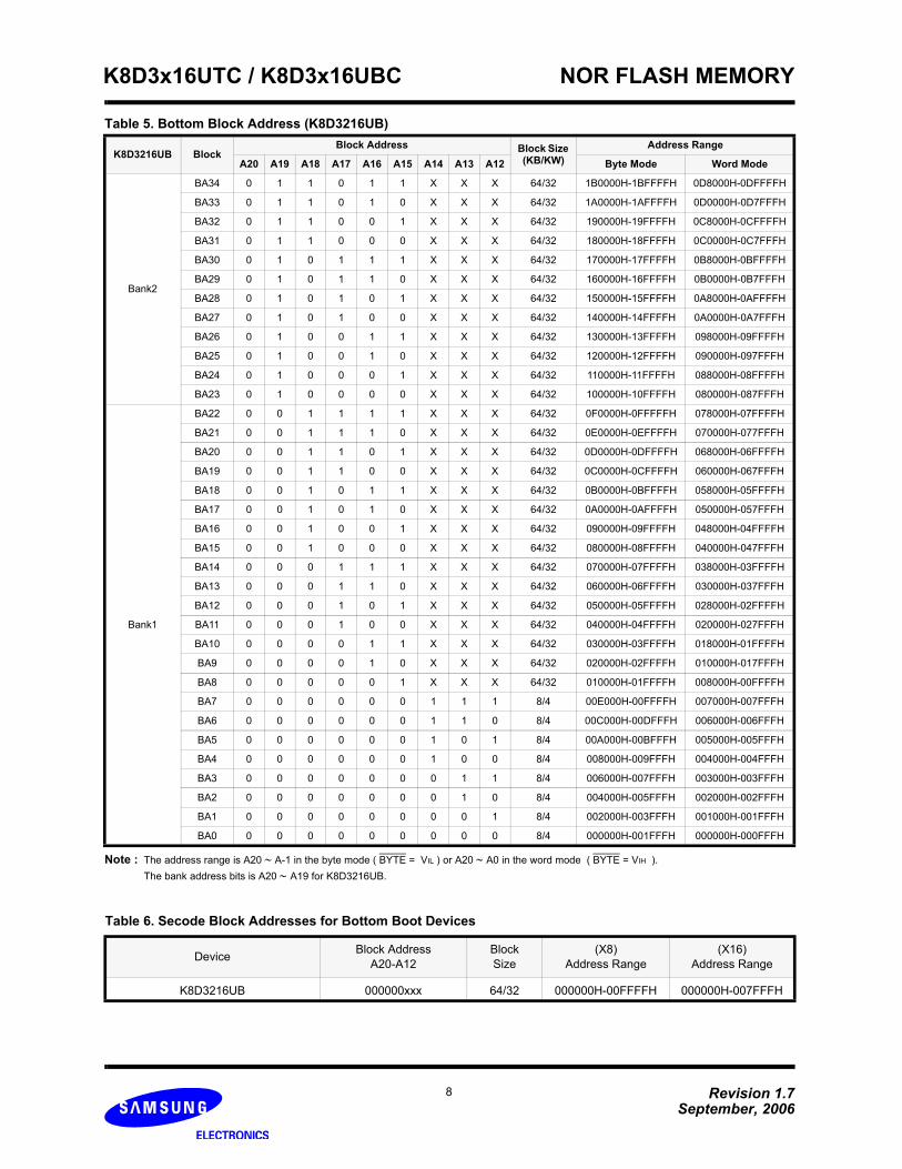
Table 5. Bottom Block Address (K8D3216UB)
Note : The address range is A20 ∼ A-1 in the byte mode ( BYTE = VIL ) or A20 ∼ A0 in the word mode ( BYTE = VIH ). The bank address bits is A20 ∼ A19 for K8D3216UB.
Table 6. Secode Block Addresses for Bottom Boot Devices
NOR FLASH MEMORYK8D3x16UTC / K8D3x16UBC
Revision 1.7September, 2006
9
PRODUCT INTRODUCTION
Table 7. Operations Table
Operation CE OE WE BYTE WP/ACC A9 A6 A1 A0 DQ15/
A-1DQ8/DQ14
DQ0/DQ7 RESET
Read word L L H H
L/HA9 A6 A1 A0 DQ15 DOUT DOUT H
byte L L H L A9 A6 A1 A0 A-1 High-Z DOUT H
Stand-by Vcc ±0.3V X X X (2) X X X X High-Z High-Z High-Z (2)
Output Disable L H H X L/H X X X X High-Z High-Z High-Z H
Reset X X X X L/H X X X X High-Z High-Z High-Z L
Writeword L H L H
(4)A9 A6 A1 A0 DIN DIN DIN H
byte L H L L A9 A6 A1 A0 A-1 High-Z DIN H
Enable Block Group Protect (3) L H L X L/H X L H L X X DIN VID
Enable Block GroupUnprotect (3) L H L X (4) X H H L X X DIN VID
Temporary Block Group X X X X (4) X X X X X X X VID
Auto Select Manufacturer ID (5) L L H X L/H VID L L L X X Code(See
Table 9) H
Auto SelectDevice Code (5) L L H X L/H VID L L H X X Code(See
Table 9) H
Notes :1. L = VIL (Low), H = VIH (High), VID = 8.5V~12.5V, DIN = Data in, DOUT = Data out, X = Don't care. 2. WP/ACC and RESET pin are asserted at Vcc±0.3 V or Vss±0.3 V in the Stand-by mode.3. Addresses must be composed of the Block address (A12 - A20). The Block Protect and Unprotect operations may be implemented via programming equipment too. Refer to the "Block Group Protection and Unprotection". 4. If WP/ACC=VIL, the two outermost boot blocks is protected. If WP/ACC=VIH, the two outermost boot block protection depends on whether those blocks were last protected or unprotected using the method described in "Block Group Protection and Unprotection". If WP/ACC=VHH, all blocks will be temporarily unprotected.5. Manufacturer and device codes may also be accessed via a command register write sequence. Refer to Table 9.
The K8D3216U is a 32Mbit (33,554,432 bits) NOR-type Flash memory. The device features single voltage power supply operatingwithin the range of 2.7V to 3.6V. The device is programmed by using the Channel Hot Electron (CHE) injection mechanism which isused to program EPROMs. The device is erased electrically by using Fowler-Nordheim tunneling mechanism. To provide highly flex-ible erase and program capability, the device adapts a block memory architecture that divides its memory array into 71 blocks (64-Kbyte x 63 , 8-Kbyte x 8). Programming is done in units of 8 bits (Byte) or 16 bits (Word). All bits of data in one or multiple blocks canbe erased simultaneously when the device executes the erase operation. To prevent the device from accidental erasing or over-writ-ing the programmed data, 71 memory blocks can be hardware protected by the block group. Byte/Word modes are available for readoperation. These modes can be selected via BYTE pin. The device provides read access times of 70ns, 80ns and 90ns supportinghigh speed microprocessors to operate without any wait states.The command set of K8D3216U is fully compatible with standard Flash devices. The device is controlled by chip enable (CE), outputenable (OE) and write enable (WE). Device operations are executed by selective command codes. The command codes to be com-bined wih addresses and data are sequentially written to the command registers using microprocessor write timing. The commandcodes serve as inputs to an internal state machine which controls the program/erase circuitry. Register contents also internally latchaddresses and data necessary to execute the program and erase operations. The K8D3216U is implemented with Internal Program/Erase Algorithms to execute the program/erase operations. The Internal Program/Erase Algorithms are invoked by program/erasecommand sequences. The Internal Program Algorithm automatically programs and verifies data at specified addresses. The InternalErase Algorithm automatically pre-programs the memory cell which is not programmed and then executes the erase operation. TheK8D3216U has means to indicate the status of completion of program/erase operations. The status can be indicated via the RY/BYpin, Data polling of DQ7, or the Toggle bit (DQ6). Once the operations have been completed, the device automatically resets itself tothe read mode. The device requires only 14 mA as active read current and 15 mA for program/erase operations.
NOR FLASH MEMORYK8D3x16UTC / K8D3x16UBC
Revision 1.7September, 2006
10
COMMAND DEFINITIONSThe K8D3216U operates by selecting and executing its operational modes. Each operational mode has its own command set. Inorder to select a certain mode, a proper command with specific address and data sequences must be written into the command reg-ister. Writing incorrect information which include address and data or writing an improper command will reset the device to the readmode. The defined valid register command sequences are stated in Table 8. Note that Erase Suspend (B0H) and Erase Resume(30H) commands are valid only while the Block Erase Operation is in progress.
Notes : 1. RA : Read Address, PA : Program Address, RD : Read Data, PD : Program Data DA : Dual Bank Address (A19 - A20), BA : Block Address (A12 - A20), X = Don’t care . 2. To terminate the Autoselect Mode, it is necessary to write Reset command to the register. 3. The 4th cycle data of Autoselect mode is output data. The 3rd and 4th cycle bank addresses of Autoselect mode must be same. 4. The Read / Program operations at non-erasing blocks and the autoselect mode are allowed in the Erase Suspend mode. 5. The Erase Suspend command is applicable only to the Block Erase operation. 6. Command is valid when the device is in read mode or Autoselect mode. 7. DQ8 - DQ15 are don’t care in command sequence, but RD and PD is excluded. 8. A11 - A20 are also don’t care, except for the case of special notice.
Description CE OE WEA20to
A12
A11to
A10A9
A8toA7
A6A5toA2
A1 A0
DQ8 to DQ15 DQ7to
DQ0BYTE=VIH
BYTE=VIL
Manufacturer ID L L H DA X VID X L X L L X X ECH
Device Code K8D3216UT (Top Boot Block) L L H DA X VID X L X L H 22H X A0H
Device Code K8D3216UB (Bottom Boot Block) L L H DA X VID X L X L H 22H X A2H
Block ProtectionVerification L L H BA X VID X L X H L X X 01H (Protected),
00H (Unprotected)
Secode Block (2)Indicator Bit (DQ7) L L H DA X VID X L X H H X X 80H (Factory locked),
00H (Not factory locked)
Table 9. K8D3216U Autoselect Codes, (High Voltage Method)
Byte/Word ModeIf the BYTE pin is set at logical "1" , the device is in word mode, DQ0-DQ15 are active. Otherwise the BYTE pin is set at logical "0" ,the device is in byte mode, DQ0-DQ7 are active. DQ8-DQ14 are in the High-Z state and DQ15 pin is used as an input for the LSB(A-1) address pin.
Read ModeThe K8D3216U is controlled by Chip Enable (CE), Output Enable (OE) and Write Enable (WE). When CE and OE are low and WEis high, the data stored at the specified address location,will be the output of the device. The outputs are in high impedance statewhenever CE or OE is high.
Standby ModeThe K8D3216U features Stand-by Mode to reduce power consumption. This mode puts the device on hold when the device is dese-lected by making CE high (CE = VIH). Refer to the DC characteristics for more details on stand-by modes.
Output DisableThe device outputs are disabled when OE is High (OE = VIH). The output pins are in high impedance state.
Automatic Sleep ModeK8D3216U features Automatic Sleep Mode to minimize the device power consumption. Since the device typically draws 5µA of thecurrent in Automatic Sleep Mode, this feature plays an extremely important role in battery-powered applications. When addressesremain steady for tAA+50ns, the device automatically activates the Automatic Sleep Mode. In the sleep mode, output data is latchedand always available to the system. When addresses are changed, the device provides new data without wait time.
DataOutputs
tAA + 50ns
Data
Auto Sleep Mode
Address
Data Data Data Data
Figure 1. Auto Sleep Mode Operation
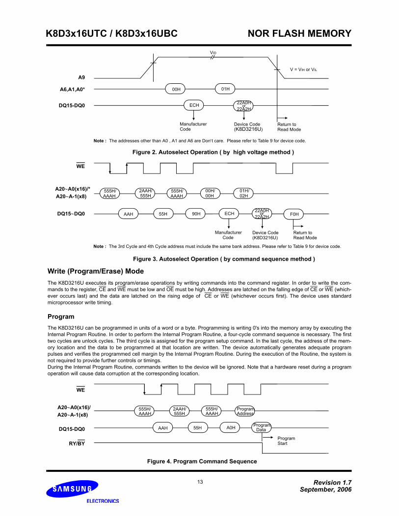
Autoselect ModeThe K8D3216U offers the Autoselect Mode to identify manufacturer and device type by reading a binary code. The Autoselect Modeallows programming equipment to automatically match the device to be programmed with its corresponding programming algorithm.In addition, this mode allows the verification of the status of write protected blocks. This mode is used by two method. The one is highvoltage method to be required VID (8.5V~12.5V) on address pin A9. When A9 is held at VID and the bank address or block address isasserted, the device outputs the valid data via DQ pins(see Table 9 and Figure 2). The rest of addresses except A0, A1 and A6 areDon′t Care. The other is autoselect command method that the autoselect code is accessible by the commamd sequence without VID.
The manufacturer and device code may also be read via the command register. The Command Sequence is shown in Table 8 andFigure 3. The autoselect operation of block protect verification is initiated by first writing two unlock cycle. The third cycle must con-tain the bank address and autoselect command (90H). If Block address while (A6, A1, A0) = (0,1,0) is finally asserted on the addresspin, it will produce a logical "1" at the device output DQ0 to indicate a write protected block or a logical "0" at the device output DQ0to indicate a write unprotected block. To terminate the autoselect operation, write Reset command (F0H) into the command register.
NOR FLASH MEMORYK8D3x16UTC / K8D3x16UBC
Revision 1.7September, 2006
13
Figure 3. Autoselect Operation ( by command sequence method )
WE
555H/AAAH
2AAH/555H
555H/AAAH
AAH 55H 90H
00H/ 01H/
ECH
ManufacturerCode
Device Code
A20∼A0(x16)/*
DQ15∼DQ0 F0H
Return toRead Mode
Write (Program/Erase) Mode The K8D3216U executes its program/erase operations by writing commands into the command register. In order to write the com-mands to the register, CE and WE must be low and OE must be high. Addresses are latched on the falling edge of CE or WE (which-ever occurs last) and the data are latched on the rising edge of CE or WE (whichever occurs first). The device uses standardmicroprocessor write timing.
ProgramThe K8D3216U can be programmed in units of a word or a byte. Programming is writing 0's into the memory array by executing theInternal Program Routine. In order to perform the Internal Program Routine, a four-cycle command sequence is necessary. The firsttwo cycles are unlock cycles. The third cycle is assigned for the program setup command. In the last cycle, the address of the mem-ory location and the data to be programmed at that location are written. The device automatically generates adequate programpulses and verifies the programmed cell margin by the Internal Program Routine. During the execution of the Routine, the system isnot required to provide further controls or timings. During the Internal Program Routine, commands written to the device will be ignored. Note that a hardware reset during a programoperation will cause data corruption at the corresponding location.
Figure 4. Program Command Sequence
WE
555H/AAAH
2AAH/555H
555H/AAAH
AAH 55H A0H
Program
Program
ProgramStart
DQ15-DQ0
Address
Data
RY/BY
A9
VID
00H 01H
ECH 22A0Hor
22A2H
ManufacturerCode
Device Code
A6,A1,A0*
DQ15-DQ0
Figure 2. Autoselect Operation ( by high voltage method )
Return toRead Mode
V = VIH or VIL
22A0Hor22A2H
Note : The addresses other than A0 , A1 and A6 are Don′t care. Please refer to Table 9 for device code.
Note : The 3rd Cycle and 4th Cycle address must include the same bank address. Please refer to Table 9 for device code.
(K8D3216U)
(K8D3216U)
A20∼A-1(x8)
A20∼A0(x16)/A20∼A-1(x8)
00H 02H
NOR FLASH MEMORYK8D3x16UTC / K8D3x16UBC
Revision 1.7September, 2006
14
Unlock BypassThe K8D3216U provides the unlock bypass mode to save its program time for program operation. The mode is invoked by the unlockbypass command sequence. Then, the unlock bypass program command sequence is required to program the device. Unlike the standard program command sequence that contains four bus cycles, the unlock bypass program command sequencecomprises only two bus cycles. The unlock bypass mode is engaged by issuing the unlock bypass command sequence which is comprised of three bus cycles. Writ-ing first two unlock cycles is followed by a third cycle containing the unlock bypass command (20H). Once the device is in the unlockbypass mode, the unlock bypass program command sequence is necessary to program in this mode. The unlock bypass programcommand sequence is comprised of only two bus cycles; writing the unlock bypass program command (A0H) is followed by the pro-gram address and data. This command sequence is the only valid one for programming the device in the unlock bypass mode.The unlock bypass reset command sequence is the only valid command sequence to exit the unlock bypass mode. The unlockbypass reset command sequence consists of two bus cycles. The first cycle must contain the data (90H). The second cycle containsonly the data (00H). Then, the device returns to the read mode.
Chip EraseTo erase a chip is to write 1′s into the entire memory array by executing the Internal Erase Routine. The Chip Erase requires six buscycles to write the command sequence. The erase set-up command is written after first two "unlock" cycles. Then, there are twomore write cycles prior to writing the chip erase command. The Internal Erase Routine automatically pre-programs and verifies theentire memory for an all zero data pattern prior to erasing. The automatic erase begins on the rising edge of the last WE or CE pulsein the command sequence and terminates when DQ7 is "1". After that the device returns to the read mode.
Figure 5. Chip Erase Command Sequence
WE
555H/AAAH
2AAH/555H
555H/AAAH
AAH 55H 80H
555H
Chip EraseStart
DQ15-DQ0
AAAH2AAH/555H
AAH 55H 10H
RY/BY
555H/AAAH
A20∼A0(x16)/A20∼A-1(x8)
Block Erase
To erase a block is to write 1′s into the desired memory block by executing the Internal Erase Routine. The Block Erase requires sixbus cycles to write the command sequence shown in Table 8. After the first two "unlock" cycles, the erase setup command (80H) iswritten at the third cycle. Then there are two more "unlock" cycles followed by the Block Erase command. The Internal Erase Routineautomatically pre-programs and verifies the entire memory prior to erasing it. The block address is latched on the falling edge of WEor CE, while the Block Erase command is latched on the rising edge of WE or CE.Multiple blocks can be erased sequentially by writing the six bus-cycle operation in Figure 6. Upon completion of the last cycle for theBlock Erase, additional block address and the Block Erase command (30H) can be written to perform the Multi-Block Erase. An 50µs(typical) "time window" is required between the Block Erase command writes. The Block Erase command must be written within the50µs "time window", otherwise the Block Erase command will be ignored. The 50µs "time window" is reset when the falling edge ofthe WE occurs within the 50µs of "time window" to latch the Block Erase command. During the 50µs of "time window", any commandother than the Block Erase or the Erase Suspend command written to the device will reset the device to read mode. After the 50µs of"time window", the Block Erase command will initiate the Internal Erase Routine to erase the selected blocks. Any Block Eraseaddress and command following the exceeded "time window" may or may not be accepted. No other commands will be recognizedexcept the Erase Suspend command during Block Erase operation.
NOR FLASH MEMORYK8D3x16UTC / K8D3x16UBC
Revision 1.7September, 2006
15
WE
555H/AAAH
2AAH/555H
555H/AAAH
AAH 55H 80H
555H/
Block EraseStart
DQ15-DQ0
AAAH2AAH/555H
BlockAddress
AAH 55H 30H
RY/BY
WE
DQ15-DQ0
Figure 7. Erase Suspend/Resume Command Sequence
Erase Suspend / ResumeThe Erase Suspend command interrupts the Block Erase to read or program data in a block that is not being erased. The Erase Sus-pend command is only valid during the Block Erase operation including the time window of 50µs. The Erase Suspend command isnot valid while the Chip Erase or the Internal Program Routine sequence is running. When the Erase Suspend command is written during a Block Erase operation, the device requires a maximum of 20µs to suspendthe erase operation. But, when the Erase Suspend command is written during the block erase time window (50µs) , the device imme-diately terminates the block erase time window and suspends the erase operation. After the erase operation has been suspended, the device is availble for reading or programming data in a block that is not beingerased. The system may also write the autoselect command sequence when the device is in the Erase Suspend mode.When the Erase Resume command is executed, the Block Erase operation will resume. When the Erase Suspend or Erase Resumecommand is executed, the addresses are in Don't Care state.
Figure 6. Block Erase Command Sequence
A20∼A0(x16)/A20∼A-1(x8)
A20∼A0(x16)/A20∼A-1(x8)
555H/AAAH
BlockAddress
AAH 30H
XXXH
EraseResume
XXXH
B0H 30H
EraseSuspend
Block EraseStart
Block EraseCommand Sequence
NOR FLASH MEMORYK8D3x16UTC / K8D3x16UBC
Revision 1.7September, 2006
16
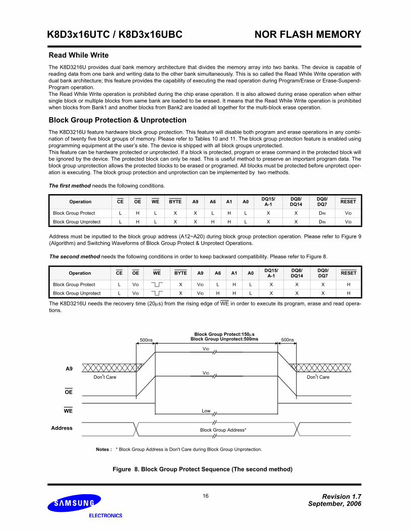
Read While WriteThe K8D3216U provides dual bank memory architecture that divides the memory array into two banks. The device is capable ofreading data from one bank and writing data to the other bank simultaneously. This is so called the Read While Write operation withdual bank architecture; this feature provides the capability of executing the read operation during Program/Erase or Erase-Suspend-Program operation.The Read While Write operation is prohibited during the chip erase operation. It is also allowed during erase operation when eithersingle block or multiple blocks from same bank are loaded to be erased. It means that the Read While Write operation is prohibitedwhen blocks from Bank1 and another blocks from Bank2 are loaded all together for the multi-block erase operation.
Block Group Protection & UnprotectionThe K8D3216U feature hardware block group protection. This feature will disable both program and erase operations in any combi-nation of twenty five block groups of memory. Please refer to Tables 10 and 11. The block group protection feature is enabled usingprogramming equipment at the user’s site. The device is shipped with all block groups unprotected.This feature can be hardware protected or unprotected. If a block is protected, program or erase command in the protected block willbe ignored by the device. The protected block can only be read. This is useful method to preserve an important program data. Theblock group unprotection allows the protected blocks to be erased or programed. All blocks must be protected before unprotect oper-ation is executing. The block group protection and unprotection can be implemented by two methods.
The first method needs the following conditions.
Operation CE OE WE BYTE A9 A6 A1 A0 DQ15/A-1
DQ8/DQ14
DQ0/DQ7 RESET
Block Group Protect L H L X X L H L X X DIN VID
Block Group Unprotect L H L X X H H L X X DIN VID
The K8D3216U needs the recovery time (20µs) from the rising edge of WE in order to execute its program, erase and read opera-tions.
Operation CE OE WE BYTE A9 A6 A1 A0 DQ15/A-1
DQ8/DQ14
DQ0/DQ7 RESET
Block Group Protect L VID X VID L H L X X X H
Block Group Unprotect L VID X VID H H L X X X H
A9
OE
Don't Care
WE
Address
Don't Care
500ns500ns
Block Group Address*
Figure 8. Block Group Protect Sequence (The second method)
Block Group Protect:150µsBlock Group Unprotect:500ms
Notes : * Block Group Address is Don't Care during Block Group Unprotection.
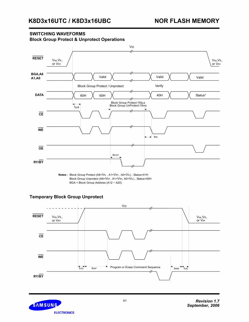
Address must be inputted to the block group address (A12~A20) during block group protection operation. Please refer to Figure 9(Algorithm) and Switching Waveforms of Block Group Protect & Unprotect Operations.
The second method needs the following conditions in order to keep backward compatibility. Please refer to Figure 8.
Low
VID
VID
NOR FLASH MEMORYK8D3x16UTC / K8D3x16UBC
Revision 1.7September, 2006
17
Figure 9. Block Group Protection & Unprotection Algorithms
Block ProtectAlgorithm
Set up Block Groupaddress
Block Group Protect:Write 60H to BlockGroup address with
A6=0,A1=1A0=0
Wait 150µs
Verify Block GroupProtect:Write 40H to Block Group address
with A6=0,A1=1,A0=0
Read fromBlock Group address
with A6=0,A1=1,A0=0
Data=01h?
Protect anotherBlock Group?
Remove VIDfrom RESET
Write RESETcommand
END
Wait 1µs
First WriteCycle=60h?
Temporary Block GroupUnprotect Mode
Block Group UnprotectWrite 60H
with A6=1,A1=1
A0=0
Wait 15ms
Verify Block GroupUnprotect:Write 40H to Block Group address
with A6=1,A1=1,A0=0
Read fromBlock Group address
with A6=1,A1=1,A0=0
Data=00h?
Last Block Group
Remove VIDfrom RESET
Write RESETcommand
END
No
IncrementCOUNT
COUNT=1000?
Device failed
No
YesYes
No
No
Yes
Algorithm
IncrementCOUNT
COUNT=25?
Device failed
No
Yes
No
All Block GroupsProtected ?
NoBlock Group <i>, i= 0
START
COUNT = 1
RESET=VID
Yes
Yes
Yes
No
Note : All blocks must be protected before unprotect operation is executing.
verified ?
Block Group Protection ?
Yes
No
Yes
Set up next Block
ResetCOUNT=1
Block Unprotect
Group address
NOR FLASH MEMORYK8D3x16UTC / K8D3x16UBC
Revision 1.7September, 2006
18
Table 10. Flash Memory Block Group Address (Top Boot Block)
Block Group Block Address
BlockA20 A19 A18 A17 A16 A15 A14 A13 A12
BGA0 0 0 0 0 0 0 X X X BA0
BGA1 0 0 0 0
0 1
X X X BA1 to BA31 0
1 1
BGA2 0 0 0 1 X X X X X BA4 to BA7
BGA3 0 0 1 0 X X X X X BA8 to BA11
BGA4 0 0 1 1 X X X X X BA12 to BA15
BGA5 0 1 0 0 X X X X X BA16 to BA19
BGA6 0 1 0 1 X X X X X BA20 to BA23
BGA7 0 1 1 0 X X X X X BA24 to BA27
BGA8 0 1 1 1 X X X X X BA28 to BA31
BGA9 1 0 0 0 X X X X X BA32 to BA35
BGA10 1 0 0 1 X X X X X BA36 to BA39
BGA11 1 0 1 0 X X X X X BA40 to BA43
BGA12 1 0 1 1 X X X X X BA44 to BA47
BGA13 1 1 0 0 X X X X X BA48 to BA51
BGA14 1 1 0 1 X X X X X BA52 to BA55
BGA15 1 1 1 0 X X X X X BA56 to BA59
BGA16 1 1 1 1
0 0
X X X BA60 to BA620 1
1 0
BGA17 1 1 1 1 1 1 0 0 0 BA63
BGA18 1 1 1 1 1 1 0 0 1 BA64
BGA19 1 1 1 1 1 1 0 1 0 BA65
BGA20 1 1 1 1 1 1 0 1 1 BA66
BGA21 1 1 1 1 1 1 1 0 0 BA67
BGA22 1 1 1 1 1 1 1 0 1 BA68
BGA23 1 1 1 1 1 1 1 1 0 BA69
BGA24 1 1 1 1 1 1 1 1 1 BA70
NOR FLASH MEMORYK8D3x16UTC / K8D3x16UBC
Revision 1.7September, 2006
19
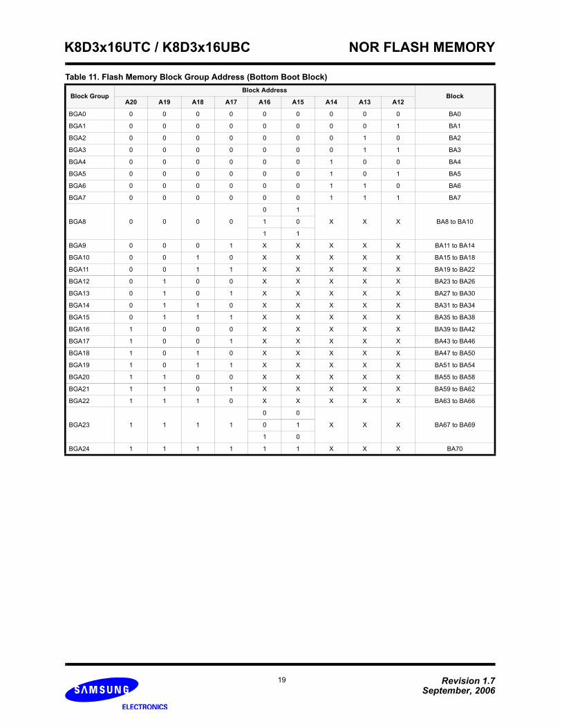
Table 11. Flash Memory Block Group Address (Bottom Boot Block)
Block Group Block Address
BlockA20 A19 A18 A17 A16 A15 A14 A13 A12
BGA0 0 0 0 0 0 0 0 0 0 BA0
BGA1 0 0 0 0 0 0 0 0 1 BA1
BGA2 0 0 0 0 0 0 0 1 0 BA2
BGA3 0 0 0 0 0 0 0 1 1 BA3
BGA4 0 0 0 0 0 0 1 0 0 BA4
BGA5 0 0 0 0 0 0 1 0 1 BA5
BGA6 0 0 0 0 0 0 1 1 0 BA6
BGA7 0 0 0 0 0 0 1 1 1 BA7
BGA8 0 0 0 0
0 1
X X X BA8 to BA101 0
1 1
BGA9 0 0 0 1 X X X X X BA11 to BA14
BGA10 0 0 1 0 X X X X X BA15 to BA18
BGA11 0 0 1 1 X X X X X BA19 to BA22
BGA12 0 1 0 0 X X X X X BA23 to BA26
BGA13 0 1 0 1 X X X X X BA27 to BA30
BGA14 0 1 1 0 X X X X X BA31 to BA34
BGA15 0 1 1 1 X X X X X BA35 to BA38
BGA16 1 0 0 0 X X X X X BA39 to BA42
BGA17 1 0 0 1 X X X X X BA43 to BA46
BGA18 1 0 1 0 X X X X X BA47 to BA50
BGA19 1 0 1 1 X X X X X BA51 to BA54
BGA20 1 1 0 0 X X X X X BA55 to BA58
BGA21 1 1 0 1 X X X X X BA59 to BA62
BGA22 1 1 1 0 X X X X X BA63 to BA66
BGA23 1 1 1 1
0 0
X X X BA67 to BA690 1
1 0
BGA24 1 1 1 1 1 1 X X X BA70
NOR FLASH MEMORYK8D3x16UTC / K8D3x16UBC
Revision 1.7September, 2006
20
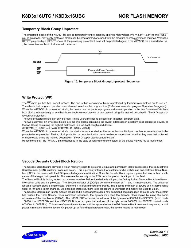
Temporary Block Group UnprotectThe protected blocks of the K8D3216U can be temporarily unprotected by applying high voltage (VID = 8.5V~12.5V) to the RESETpin. In this mode, previously protected blocks can be programmed or erased with the program or erase command routines. When theRESET pin goes high (RESET = VIH), all the previously protected blocks will be protected again. If the WP/ACC pin is asserted at VIL
, the two outermost boot blocks remain protected.
RESET
Program & Erase Operation
VID
V = VIH or VIL
at Protected BlockCEWE
Figure 10. Temporary Block Group Unprotect Sequence
Secode(Security Code) Block RegionThe Secode Block feature provides a Flash memory region to be stored unique and permanent identification code, that is, ElectronicSerial Number (ESN), customer code and so on. This is primarily intended for customers who wish to use an Electronic Serial Num-ber (ESN) in the device with the ESN protected against modification. Once the Secode Block region is protected, any further modifi-cation of that region is impossible. This ensures the security of the ESN once the product is shipped to the field.The Secode Block is factory locked or customer lockable. Before the device is shipped, the factory locked Secode Block is written onthe special code and it is protected. The Secode Indicator bit (DQ7) is permanently fixed at "1" and it is not changed. The customerlockable Secode Block is unprotected, therefore it is programmed and erased. The Secode Indicator bit (DQ7) of it is permanentlyfixed at "0" and it is not changed. But once it is protected, there is no procedure to unprotect and modify the Secode Block. The Secode Block region is 64K bytes in length and is accessed through a new command sequence (see Table 8). After the systemhas written the Enter Secode Block command sequence, the system may read the Secode Block region by using the sameaddresses of the boot blocks (8KBx8). The K8D3216UT occupies the address of the byte mode 3F0000H to 3FFFFFH (word mode1F8000H to 1FFFFFH) and the K8D3216UB type occupies the address of the byte mode 000000H to 00FFFFH (word mode000000H to 007FFFH). This mode of operation continues until the system issues the Exit Secode Block command sequence, or untilpower is removed from the device. On power-up, or following a hardware reset, the device reverts to read mode.
Write Protect (WP)The WP/ACC pin has two useful functions. The one is that certain boot block is protected by the hardware method not to use VID.The other is that program operation is accelerated to reduce the program time (Refer to Accelerated program Operation Paragraph). When the WP/ACC pin is asserted at VIL, the device can not perform program and erase operation in the two "outermost" 8K byteboot blocks independently of whether those blocks were protected or unprotected using the method described in "Block Group pro-tection/Unprotection".The write protected blocks can only be read. This is useful method to preserve an important program data.The two outermost 8K byte boot blocks are the two blocks containing the lowest addresses in a bottom-boot-configured device, orthe two blocks containing the highest addresses in a top-boot-congfigured device.(K8D3216UT : BA69 and BA70, K8D3216UB : BA0 and BA1)When the WP/ACC pin is asserted at VIH, the device reverts to whether the two outermost 8K byte boot blocks were last set to beprotected or unprotected. That is, block protection or unprotection for these two blocks depends on whether they were last protectedor unprotected using the method described in "Block Group protection/unprotection". Recommend that the WP/ACC pin must not be in the state of floating or unconnected, or the device may be led to malfunction.
NOR FLASH MEMORYK8D3x16UTC / K8D3x16UBC
Revision 1.7September, 2006
21
Accelerated Program OperationAccelerated program operation reduces the program time. This is one of two functions provided by the WP/ACC pin. When the WP/ACC pin is asserted as VHH, the device automatically enters the aforementioned Unlock Bypass mode, temporarily unprotecting anyprotected blocks, and reduces the program operation time. The system would use a two-cycle program command sequence asrequired by the Unlock Bypass mode. Removing VHH from the WP/ACC pin returns the device to normal operation. Recommendthat the WP/ACC pin must not be asserted at VHH except accelerated program operation, or the device may be damaged. Inaddition, the WP/ACC pin must not be in the state of floating or unconnected, otherwise the device may be led to malfunc-tion.
Software Reset
The reset command provides that the bank is reseted to read mode or erase-suspend-read mode. The addresses are in Don't Carestate. The reset command is vaild between the sequence cycles in an erase command sequence before erasing begins, or in a pro-gram command sequence before programming begins. This resets the bank in which was operating to read mode. if the device is beerasing or programming, the reset command is invalid until the operation is completed. Also, the reset command is valid between thesequence cycles in an autoselect command sequence. In the autoselect mode, the reset command returns the bank to read mode.If a bank entered the autoselect mode in the Erase Suspend mode, the reset command returns the bank to erase-suspend-readmode. If DQ5 is high on erase or program operation, the reset command return the bank to read mode or erase-suspend-read modeif the bank was in the Erase Suspend state.
Hardware Reset
The K8D3216U offers a reset feature by driving the RESET pin to VIL. The RESET pin must be kept low (VIL) for at least 500ns.When the RESET pin is driven low, any operation in progress will be terminated and the internal state machine will be reset to thestandby mode after 20µs. If a hardware reset occurs during a program operation, the data at that particular location will be lost.Once the RESET pin is taken high, the device requires 200ns of wake-up time until outputs are valid for read access. Also, note thatall the data output pins are tri-stated for the duration of the RESET pulse. The RESET pin may be tied to the system reset pin. If a system reset occurs during the Internal Program and Erase Routine, thedevice will be automatically reset to the read mode ; this will enable the systems microprocessor to read the boot-up firmware fromthe Flash memory.
Power-up ProtectionTo avoid initiation of a write cycle during Vcc Power-up, RESET low must be asserted during power-up. After RESET goes high, thedevice is reset to the read mode.
Low Vcc Write InhibitTo avoid initiation of a write cycle during Vcc power-up and power-down, a write cycle is locked out for Vcc less than 1.8V. If Vcc <VLKO (Lock-Out Voltage), the command register and all internal program/erase circuits are disabled. Under this condition the devicewill reset itself to the read mode. Subsequent writes will be ignored until the Vcc level is greater than VLKO. It is the user′s responsi-bility to ensure that the control pins are logically correct to prevent unintentional writes when Vcc is above 1.8V.
Write Pulse Glitch ProtectionNoise pulses of less than 5ns(typical) on CE, OE, or WE will not initiate a write cycle.
Logical Inhibit
Writing is inhibited under any one of the following conditions : OE = VIL, CE = VIH or WE = VIH. To initiate a write, CE and WE mustbe "0", while OE is "1".
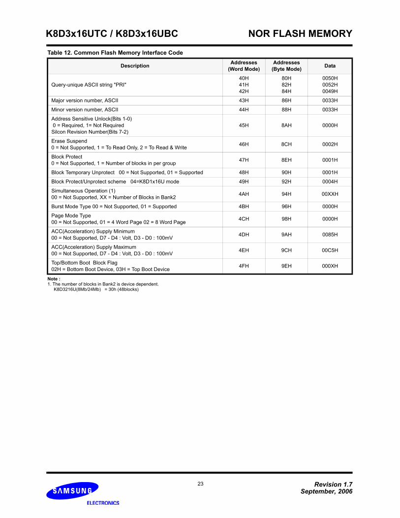
Commom Flash Memory InterfaceCommon Flash Momory Interface is contrived to increase the compatibility of host system software. It provides the specific informa-tion of the device, such as memory size, byte/word configuration, and electrical features. Once this information has been obtained,the system software will know which command sets to use to enable flash writes, block erases, and control the flash component. When the system writes the CFI command(98H) to address 55H in word mode(or address AAH in byte mode), the device enters theCFI mode. And then if the system writes the address shown in Table 12, the system can read the CFI data. Query data are alwayspresented on the lowest-order data outputs(DQ0-7) only. In word(x16) mode, the upper data outputs(DQ8-15) is 00h. To terminatethis operation, the system must write the reset command.
NOR FLASH MEMORYK8D3x16UTC / K8D3x16UBC
Revision 1.7September, 2006
22
Table 12. Common Flash Memory Interface Code
Description Addresses(Word Mode)
Addresses(Byte Mode) Data
Query Unique ASCII string "QRY"10H11H12H
20H22H24H
0051H0052H0059H
Primary OEM Command Set 13H14H
26H28H
0002H0000H
Address for Primary Extended Table 15H16H
2AH2CH
0040H0000H
Alternate OEM Command Set (00h = none exists) 17H18H
DEVICE STATUS FLAGSThe K8D3216U has means to indicate its status of operation in the bank where a program or erase operation is in processes.Address must include bank address being excuted internal routine operation. The status is indicated by raising the device status flagvia corresponding DQ pins or the RY/ BY pin. The corresponding DQ pins are DQ7, DQ6, DQ5, DQ3 and DQ2. The statuses are asfollows :
Table 13. Hardware Sequence Flags
Notes : 1. DQ2 will toggle when the device performs successive read operations from the erase suspended block. 2. If DQ5 is High (exceeded timing limits), successive reads from a problem block will cause DQ2 to toggle.
Erase Suspend Read Non-Erase Sus-pended Block Data Data Data Data Data 1
Erase SuspendProgram
Non-Erase Sus-pended Block DQ7 Toggle 0 0 1 0
ExceededTime Limits
Programming DQ7 Toggle 1 0 No Toggle 0
Block Erase or Chip Erase 0 Toggle 1 1 (Note 2) 0
Erase Suspend Program DQ7 Toggle 1 0 No Toggle 0
DQ7 : Data PollingWhen an attempt to read the device is made while executing the Internal Program, the complement of the data is written to DQ7 asan indication of the Routine in progress. When the Routine is completed an attempt to access to the device will produce the true datawritten to DQ7. When a user attempts to read the device during the Erase operation, DQ7 will be low. If the device is placed in theErase Suspend Mode, the status can be detected via the DQ7 pin. If the system tries to read an address which belongs to a blockthat is being erased, DQ7 will be high. If a non-erased block address is read, the device will produce the true data to DQ7. If anattempt is made to program a protected block, DQ7 outputs complements the data for approximately 1µs and the device then returnsto the Read Mode without changing data in the block. If an attempt is made to erase a protected block, DQ7 outputs complementdata in approximately 100us and the device then returns to the Read Mode without erasing the data in the block.
DQ6 : Toggle Bit Toggle bit is another option to detect whether an Internal Routine is in progress or completed. Once the device is at a busy state,DQ6 will toggle. Toggling DQ6 will stop after the device completes its Internal Routine. If the device is in the Erase Suspend Mode,an attempt to read an address that belongs to a block that is being erased will produce a high output of DQ6. If an address belongsto a block that is not being erased, toggling is halted and valid data is produced at DQ6.If an attempt is made to program a protected block, DQ6 toggles for approximately 1us and the device then returns to the ReadMode without changing the data in the block. If an attempt is made to erase a protected block, DQ6 toggles for approximately 100µsand the device then returns to the Read Mode without erasing the data in the block.
DQ5 : Exceed Timing LimitsIf the Internal Program/Erase Routine extends beyond the timing limits, DQ5 will go High, indicating program/erase failure.
NOR FLASH MEMORYK8D3x16UTC / K8D3x16UBC
Revision 1.7September, 2006
25
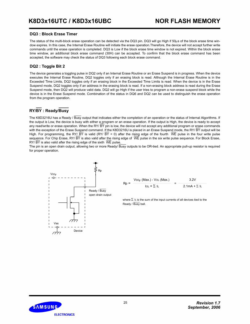
RY/BY : Ready/BusyThe K8D3216U has a Ready / Busy output that indicates either the completion of an operation or the status of Internal Algorithms. Ifthe output is Low, the device is busy with either a program or an erase operation. If the output is High, the device is ready to acceptany read/write or erase operation. When the RY/ BY pin is low, the device will not accept any additional program or erase commandswith the exception of the Erase Suspend command. If the K8D3216U is placed in an Erase Suspend mode, the RY/ BY output will beHigh. For programming, the RY/ BY is valid (RY/ BY = 0) after the rising edge of the fourth WE pulse in the four write pulsesequence. For Chip Erase, RY/ BY is also valid after the rising edge of WE pulse in the six write pulse sequence. For Block Erase,RY/ BY is also valid after the rising edge of the sixth WE pulse.The pin is an open drain output, allowing two or more Ready/ Busy outputs to be OR-tied. An appropriate pull-up resistor is requiredfor proper operation.
DQ3 : Block Erase TimerThe status of the multi-block erase operation can be detected via the DQ3 pin. DQ3 will go High if 50µs of the block erase time win-dow expires. In this case, the Internal Erase Routine will initiate the erase operation.Therefore, the device will not accept further writecommands until the erase operation is completed. DQ3 is Low if the block erase time window is not expired. Within the block erasetime window, an additional block erase command (30H) can be accepted. To confirm that the block erase command has beenaccepted, the software may check the status of DQ3 following each block erase command.
DQ2 : Toggle Bit 2The device generates a toggling pulse in DQ2 only if an Internal Erase Routine or an Erase Suspend is in progress. When the deviceexecutes the Internal Erase Routine, DQ2 toggles only if an erasing block is read. Although the Internal Erase Routine is in theExceeded Time Limits, DQ2 toggles only if an erasing block in the Exceeded Time Limits is read. When the device is in the EraseSuspend mode, DQ2 toggles only if an address in the erasing block is read. If a non-erasing block address is read during the EraseSuspend mode, then DQ2 will produce valid data. DQ2 will go High if the user tries to program a non-erase suspend block while thedevice is in the Erase Suspend mode. Combination of the status in DQ6 and DQ2 can be used to distinguish the erase operationfrom the program operation.
VccF
Ready / Busyopen drain output
Device
Vss
where Σ IL is the sum of the input currents of all devices tied to the Ready / Busy ball.
Rp
Rp =VccF (Max.) - VOL (Max.)
IOL + Σ IL =
3.2V
2.1mA + Σ IL
NOR FLASH MEMORYK8D3x16UTC / K8D3x16UBC
Revision 1.7September, 2006
26
Figure 13. Temporary Block Group Unprotect Routine
Start
RESET=VID
Notes : 1. All protected block groups are unprotected. ( If WP/ACC = VIL , the two outermost boot blocks remain protected ) 2. All previously protected block groups are protected once again.
(Note 1)
Perform Erase orProgram Operations
Temporary BlockUnprotect Completed
(Note 2)
RESET=VIH
Start
DQ7 = Data ?
No
DQ5 = 1 ?
Fail Pass
Yes
Figure 11. Data Polling Algorithms Figure 12. Toggle Bit Algorithms
DQ7 = Data ?
No
No
Yes
Read(DQ0~DQ7)Valid Address
Read(DQ0~DQ7)Valid Address
Start
DQ6 = Toggle ?
No
DQ5 = 1 ?
Fail Pass
No
DQ6 = Toggle ?
Yes
Yes
No
Read twice(DQ0~DQ7)Valid Address
Read(DQ0~DQ7)Valid Address
Yes Yes
Read(DQ0~DQ7)Valid Address
NOR FLASH MEMORYK8D3x16UTC / K8D3x16UBC
Revision 1.7September, 2006
27
DC CHARACTERISTICS
RECOMMENDED OPERATING CONDITIONS ( Voltage reference to Vss )
Parameter Symbol Min Typ. Max Unit
Supply Voltage VCC 2.7 3.0 3.6 V
Supply Voltage VSS 0 0 0 V
ABSOLUTE MAXIMUM RATINGS
Notes : 1. Minimum DC voltage is -0.5V on Input/ Output pins. During transitions, this level may fall to -2.0V for periods <20ns. Maximum DC voltage on input / output pins is Vcc+0.5V which, during transitions, may overshoot to Vcc+2.0V for periods <20ns.2. Minimum DC voltage is -0.5V on A9, OE, RESET and WP/ACC pins. During transitions, this level may fall to -2.0V for periods <20ns. Maximum DC voltage on A9, OE, RESET pins is 12.5V which, during transitions, may overshoot to 14.0V for periods <20ns. 3. Permanent device damage may occur if ABSOLUTE MAXIMUM RATINGS are exceeded. Functional operation should be restricted to the conditions detailed in the operational sections of this data sheet. Exposure to absolute maximum rating conditions for extended periods may affect reliability.
Parameter Symbol Rating Unit
Voltage on any pin relative to VSS
Vcc Vcc -0.5 to +4.0
VA9, OE , RESET
VIN
-0.5 to +12.5
WP/ACC -0.5 to +12.5
All Other Pins -0.5 to +4.0
Temperature Under BiasCommercial
Tbias-10 to +125
°CIndustrial -40 to +125
Storage Temperature Tstg -65 to +150 °C
Short Circuit Output Current IOS 5 mA
Operating TemperatureTA (Commercial Temp.) 0 to +70 °C
TA (Industrial Temp.) -40 to + 85 °C
Parameter Symbol Test Conditions Min Typ Max Unit
Input Leakage Current ILI VIN=VSS to VCC, VCC=VCCmax − 1.0 - + 1.0 µA
Voltage for WP/ACC Block Tempo-rarily Unprotect and Program Accel-eration (4)
VHH VCC = 3.0V ± 0.3V 8.5 - 12.5 V
NOR FLASH MEMORYK8D3x16UTC / K8D3x16UBC
Revision 1.7September, 2006
28
AC CHARACTERISTICS
AC TEST CONDITIONParameter Value
Input Pulse Levels 0V to Vcc
Input Rise and Fall Times 5ns
Input and Output Timing Levels Vcc/2
Output Load CL = 30pF
Read Operations
Note : 1. Not 100% tested.
Parameter Symbol
VCC=2.7V~3.6V
Unit-7 -8 -9
Min Max Min Max Min Max
Read Cycle Time (1) tRC 70 - 80 - 90 - ns
Address Access Time tAA - 70 - 80 - 90 ns
Chip Enable Access Time tCE - 70 - 80 - 90 ns
Output Enable Time tOE - 25 - 25 - 35 ns
CE & OE Disable Time (1) tDF - 16 - 16 - 16 ns
Output Hold Time from Address, CE or OE (1) tOH 0 - 0 - 0 - ns
Notes :1. The ICC current listed includes both the DC operating current and the frequency dependent component(at 5 MHz). The read current is typically 14 mA (@ VCC=3.0V , OE at VIH.)2. ICC active during Internal Routine(program or erase) is in progress.3. ICC active during Read while Write is in progress.4. The high voltage ( VHH or VID ) must be used in the range of Vcc = 3.0V ± 0.3V 5. Not 100% tested.6. Typical value are measured at Vcc = 3.0V,TA=25°C , Not 100% tested.
CAPACITANCE(TA = 25 °C, VCC = 3.3V, f = 1.0MHz)
Note : Capacitance is periodically sampled and not 100% tested.
Item Symbol Test Condition Min Max Unit
Input Capacitance CIN VIN=0V - 10 pF
Output Capacitance COUT VOUT=0V - 10 pF
Control Pin Capacitance CIN2 VIN=0V - 10 pF
Parameter Symbol Test Conditions Min Typ Max UnitVoltage for Autoselect and Block Protect (4) VID VCC = 3.0V ± 0.3V 8.5 - 12.5 V
Output Low Level VOL IOL=100µA, VCC=VCCmin - - 0.4 V
Output High Level VOH IOH=-100µA, Vcc = VCCmin VCC-0.4 - - V
Low Vcc Lock-out Voltage (5) VLKO 1.8 - 2.5 V
0V
Vcc
Vcc/2 Vcc/2
Input Pulse and Test Point
Input & OutputTest Point
Output Load
* CL= 30pF including ScopeCL
Device
and Jig Capacitance
NOR FLASH MEMORYK8D3x16UTC / K8D3x16UBC
Revision 1.7September, 2006
29
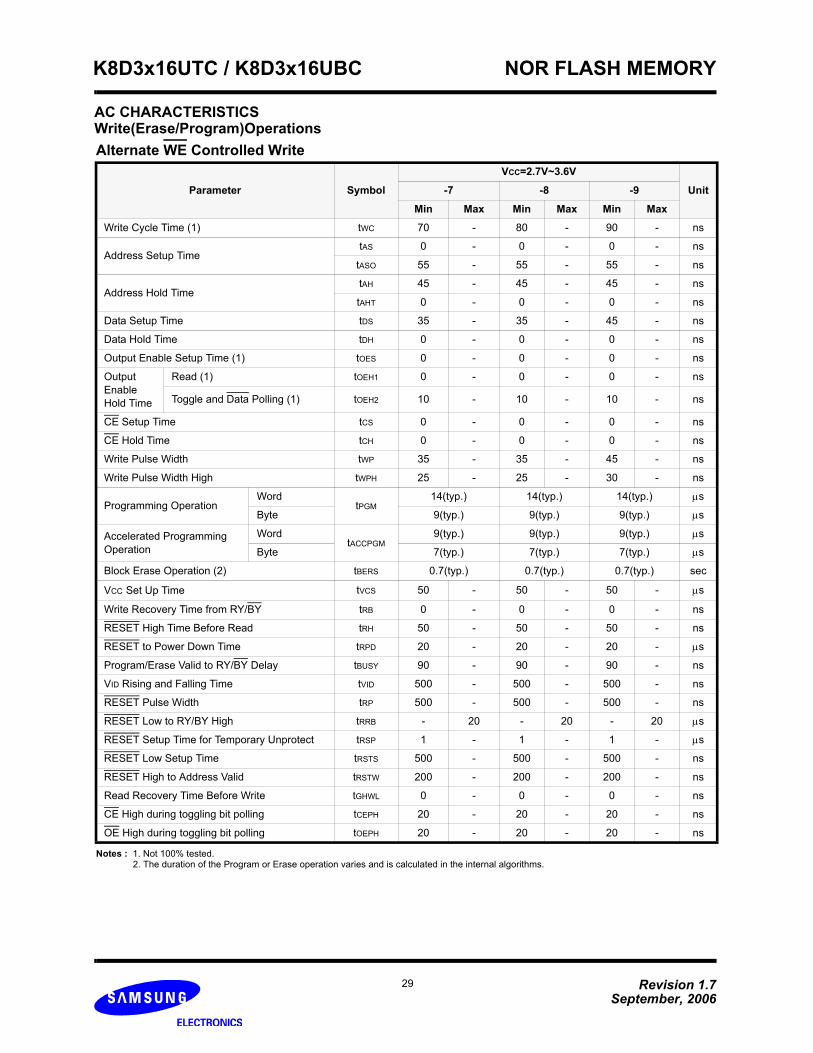
Alternate WE Controlled Write
Notes : 1. Not 100% tested.2. The duration of the Program or Erase operation varies and is calculated in the internal algorithms.
Parameter Symbol
VCC=2.7V~3.6V
Unit-7 -8 -9
Min Max Min Max Min Max
Write Cycle Time (1) tWC 70 - 80 - 90 - ns
Address Setup TimetAS 0 - 0 - 0 - ns
tASO 55 - 55 - 55 - ns
Address Hold TimetAH 45 - 45 - 45 - ns
tAHT 0 - 0 - 0 - ns
Data Setup Time tDS 35 - 35 - 45 - ns
Data Hold Time tDH 0 - 0 - 0 - ns
Output Enable Setup Time (1) tOES 0 - 0 - 0 - ns
Output Enable Hold Time
Read (1) tOEH1 0 - 0 - 0 - ns
Toggle and Data Polling (1) tOEH2 10 - 10 - 10 - ns
Notes : 1. 25 °C, VCC = 3.0V 100,000 cycles, typical pattern. 2. System-level overhead is defined as the time required to execute the four bus cycle command necessary to program each byte. In the preprogramming step of the Internal Erase Routine, all bytes are programmed to 00H before erasure.
ParameterLimits
Unit CommentsMin Typ Max
Block Erase Time - 0.7 15 sec Excludes 00H programmingprior to erasure
Chip Erase Time - 49 - sec
Word Programming Time - 14 330 µs Excludes system-level overhead
Byte Programming Time - 9 210 µs Excludes system-level overhead
Accelerated Byte/Word Program Time
Word Mode - 9 210 µs Excludes system-level overhead
Output Hold Time from Address, CE or OE tOH 0 - 0 - 0 - ns
OE Hold Time tOEH1 0 - 0 - 0 - ns
NOTEAsynchronous mode may not support read following four sequential invalid read condition within 200ns.
NOR FLASH MEMORYK8D3x16UTC / K8D3x16UBC
Revision 1.7September, 2006
32
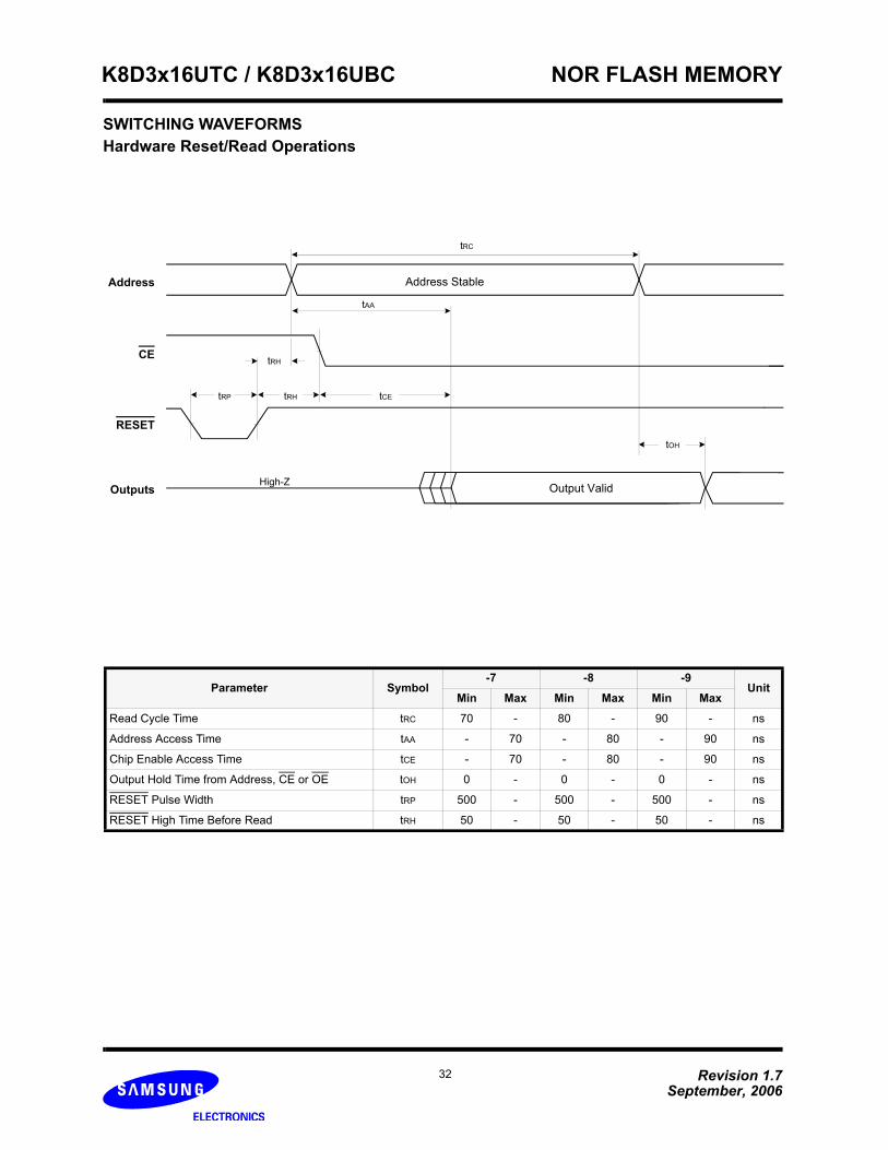
Hardware Reset/Read OperationsSWITCHING WAVEFORMS
Parameter Symbol-7 -8 -9
UnitMin Max Min Max Min Max
Read Cycle Time tRC 70 - 80 - 90 - ns
Address Access Time tAA - 70 - 80 - 90 ns
Chip Enable Access Time tCE - 70 - 80 - 90 ns
Output Hold Time from Address, CE or OE tOH 0 - 0 - 0 - ns
RESET Pulse Width tRP 500 - 500 - 500 - ns
RESET High Time Before Read tRH 50 - 50 - 50 - ns
RESET
Address
CE
OutputsHigh-Z
tRC
Address Stable
tAA
tCE
tOH
tRH
tRHtRP
Output Valid
NOR FLASH MEMORYK8D3x16UTC / K8D3x16UBC
Revision 1.7September, 2006
33
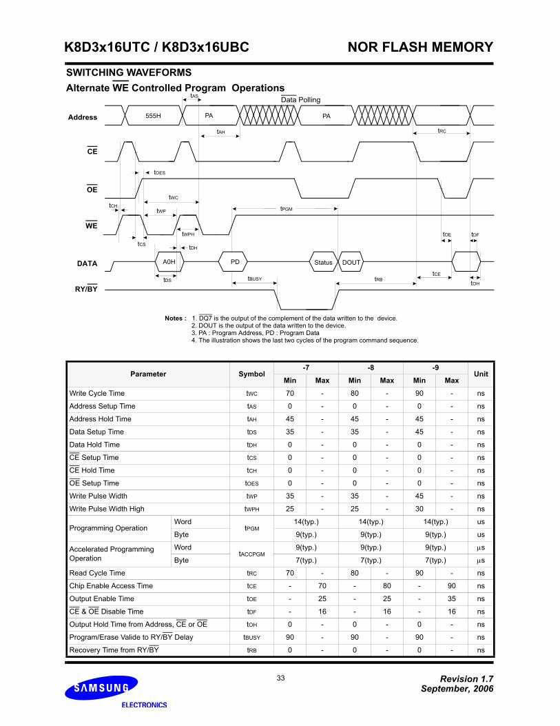
Alternate WE Controlled Program OperationsSWITCHING WAVEFORMS
Notes : 1. DQ7 is the output of the complement of the data written to the device. 2. DOUT is the output of the data written to the device. 3. PA : Program Address, PD : Program Data 4. The illustration shows the last two cycles of the program command sequence.
OE
Address
tCS
CE
DATA
WE
tAH
tOH
tDF
tAS
tRC
tOE
tCEtDS
tDH
tWP
tOES
tPGM
Status DOUT
555H PA PA
A0H
Data Polling
tCH
PD
tWPH
RY/BYtBUSY tRB
tWC
Parameter Symbol-7 -8 -9
UnitMin Max Min Max Min Max
Write Cycle Time tWC 70 - 80 - 90 - ns
Address Setup Time tAS 0 - 0 - 0 - ns
Address Hold Time tAH 45 - 45 - 45 - ns
Data Setup Time tDS 35 - 35 - 45 - ns
Data Hold Time tDH 0 - 0 - 0 - ns
CE Setup Time tCS 0 - 0 - 0 - ns
CE Hold Time tCH 0 - 0 - 0 - ns
OE Setup Time tOES 0 - 0 - 0 - ns
Write Pulse Width tWP 35 - 35 - 45 - ns
Write Pulse Width High tWPH 25 - 25 - 30 - ns
Programming OperationWord
tPGM14(typ.) 14(typ.) 14(typ.) us
Byte 9(typ.) 9(typ.) 9(typ.) us
Accelerated Programming Operation
WordtACCPGM
9(typ.) 9(typ.) 9(typ.) µs
Byte 7(typ.) 7(typ.) 7(typ.) µs
Read Cycle Time tRC 70 - 80 - 90 - ns
Chip Enable Access Time tCE - 70 - 80 - 90 ns
Output Enable Time tOE - 25 - 25 - 35 ns
CE & OE Disable Time tDF - 16 - 16 - 16 ns
Output Hold Time from Address, CE or OE tOH 0 - 0 - 0 - ns
Alternate CE Controlled Program OperationsSWITCHING WAVEFORMS
Notes : 1. DQ7 is the output of the complement of the data written to the device.2. DOUT is the output of the data written to the device. 3. PA : Program Address, PD : Program Data4. The illustration shows the last two cycles of the program command sequence.
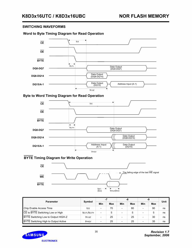
BYTE Switching High to Output Active tFHQV - 25 - 25 - 35 ns
OE
tFLQZ
CE
DQ0-DQ7
BYTE
WE
BYTE Timing Diagram for Write Operation
The falling edge of the last WE signal
CE
BYTE
tHOLD(tAH)
DQ15/A-1
tELFL
Address Input (A-1)
tSET(tAS)
Word to Byte Timing Diagram for Read Operation
Byte to Word Timing Diagram for Read Operation
Data Output(DQ0-DQ7)
DQ8-DQ14 Data Output(DQ8-DQ14)
Data Output(DQ15)
OE
tFHQV
CE
DQ0-DQ7
BYTE
DQ15/A-1
tELFH
Data Output
DQ8-DQ14
Address Input(A-1)
Data Output(DQ8-DQ14)
(DQ15)
tCE
tCE
Data Output(DQ0-DQ7)
NOR FLASH MEMORYK8D3x16UTC / K8D3x16UBC
Revision 1.7September, 2006
36
SWITCHING WAVEFORMSChip/Block Erase Operations
Parameter Symbol-7 -8 -9
UnitMin Max Min Max Min Max
Write Cycle Time tWC 70 - 80 - 90 - ns
Address Setup Time tAS 0 - 0 - 0 - ns
Address Hold Time tAH 45 - 45 - 45 - ns
Data Setup Time tDS 35 - 35 - 45 - ns
Data Hold Time tDH 0 - 0 - 0 - ns
OE Setup Time tOES 0 - 0 - 0 - ns
CE Setup Time tCS 0 - 0 - 0 - ns
Write Pulse Width tWP 35 - 35 - 45 - ns
Write Pulse Width High tWPH 25 - 25 - 30 - ns
Read Cycle Time tRC 70 - 80 - 90 - ns
VCC Set Up Time tVCS 50 - 50 - 50 - µs
OE
Address
tCS
CE
DATA
WE
tAH
tAS
tRC
tDS
tDH
80H AAHAAH 55H 30H
10H for Chip Erase
555H 2AAH 555H 555H 2AAH BA
555H for Chip Erase
tWPH
tWP
tOES
55H
RY/BY
tWC
tVCSVcc
Note : BA : Block Address
NOR FLASH MEMORYK8D3x16UTC / K8D3x16UBC
Revision 1.7September, 2006
37
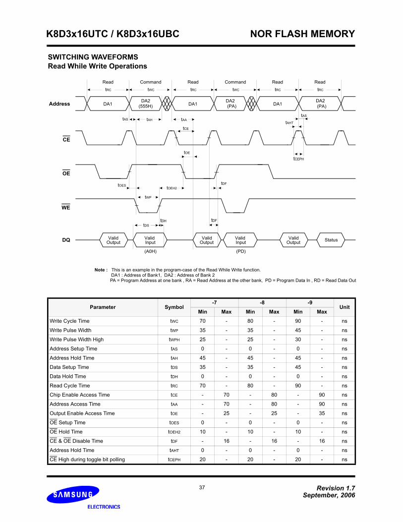
Read While Write OperationsSWITCHING WAVEFORMS
Parameter Symbol-7 -8 -9
UnitMin Max Min Max Min Max
Write Cycle Time tWC 70 - 80 - 90 - ns
Write Pulse Width tWP 35 - 35 - 45 - ns
Write Pulse Width High tWPH 25 - 25 - 30 - ns
Address Setup Time tAS 0 - 0 - 0 - ns
Address Hold Time tAH 45 - 45 - 45 - ns
Data Setup Time tDS 35 - 35 - 45 - ns
Data Hold Time tDH 0 - 0 - 0 - ns
Read Cycle Time tRC 70 - 80 - 90 - ns
Chip Enable Access Time tCE - 70 - 80 - 90 ns
Address Access Time tAA - 70 - 80 - 90 ns
Output Enable Access Time tOE - 25 - 25 - 35 ns
OE Setup Time tOES 0 - 0 - 0 - ns
OE Hold Time tOEH2 10 - 10 - 10 - ns
CE & OE Disable Time tDF - 16 - 16 - 16 ns
Address Hold Time tAHT 0 - 0 - 0 - ns
CE High during toggle bit polling tCEPH 20 - 20 - 20 - ns
Note : This is an example in the program-case of the Read While Write function. DA1 : Address of Bank1, DA2 : Address of Bank 2 PA = Program Address at one bank , RA = Read Address at the other bank, PD = Program Data In , RD = Read Data Out
OE
CE
DQ
WE
tRC
Read Command CommandRead Read Read
tAH tAA
tCE
tAS
tAHTtAS
tCEPH
tOE
tOES
tWP
tOEH2tDF
tDStDH tDF
DA1DA2
DA1 DA1DA2 DA2
(555H) (PA) (PA)
ValidOutput
ValidOutput
ValidInput
ValidOutput
ValidInput Status
Address
(A0H) (PD)
tRCtRC tRCtWC tWC
NOR FLASH MEMORYK8D3x16UTC / K8D3x16UBC
Revision 1.7September, 2006
38
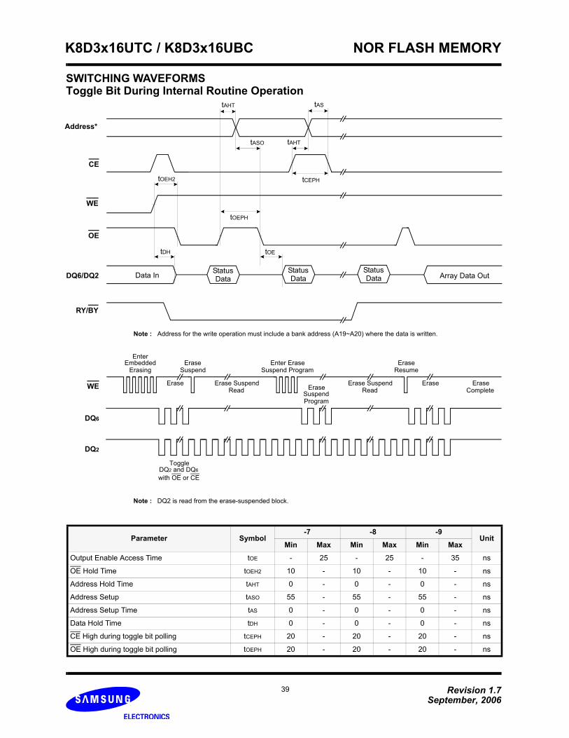
Data Polling During Internal Routine OperationSWITCHING WAVEFORMS