• 16-, 20-, 24-, and 32-Bit Word Sizes• 8 channel Programmable Audio Digital SignalProcessor (DSP) • 64-fS, 128-fS, 192-fS, and 256-fS SCLK to
Support Discrete 4 channel TDM, 6 channel• 135-MHz Maximum Speed, >2800 ProcessingTDM, and 8 channel TDM Data-TransferCycles Per Sample at 48 kHzFormats• Sample Rates of 32 kHz to 192 kHz
• Two I2C Ports for Slave or Master Download• 48-Bit Data Path and 28-Bit Coefficients• Soft Volume Controller• Single-Cycle, 76-Bit Multiply Accumulate• Dither Generator• Five Simultaneous Operations Per Clock Cycle• Efficient log2/2x Estimator• 1022 Words of 48-Bit Data Memory• Single 3.3-V Power Supply• 1022 Words of 28-Bit Coefficient Memory• 38-Pin Thin Shrink Small-Outline Package• 3K Words of 54-Bit Program RAM
(TSSOP) (DCP)• 5.88K Words of 24-Bit Delay Memory• AEC-Q100 (Grade 2: –40°C to 105°C)(122.5 ms at 48 kHz)
Compliant for Automotive Applications• 15 Stereo/TDM Data Formats(TAS3108IA)
• Independent Input/Output Data Formats
• Automotive Sound Systems• Digital Televisions• Home Theater Systems• Mini-Component Audio
Please be aware that an important notice concerning availability, standard warranty, and use in critical applications of TexasInstruments semiconductor products and disclaimers thereto appears at the end of this document.
TAS3108, TAS3108IAAUDIO DIGITAL SIGNAL PROCESSORSSLES152B–OCTOBER 2005–REVISED NOVEMBER 2007
1 Introduction ............................................... 1 7 I2C Register Map........................................ 371.1 Features .............................................. 1 7.1 Clock Control Register (0x00) ...................... 381.2 Applications........................................... 1 7.2 Status Register (0x02) .............................. 41
7.3 I2C Memory Load Control and Data Registers (0x042 Functional Description ................................. 3and 0x05)............................................ 422.1 Device Description.................................... 3
7.4 Memory Access Registers (0x06 and 0x07) ........ 432.2 Power Supply ......................................... 48 Electrical Specifications .............................. 442.3 Clock Control ......................................... 4
8.1 Absolute Maximum Ratings Over Operating2.4 Serial Audio Ports (SAPs) ............................ 4Temperature Range (unless otherwise noted) ...... 44
(TAS3108/TAS3108IA) .............................. 473.5 Power Down (PDN)................................... 88.5.3 Serial Audio Port Master Mode Signals
3.6 I2C Bus Control (CS0) ................................ 8 (TAS3108/TAS3108IA) .............................. 483.7 Programmable General Purpose I/O (GPIO) ......... 8 8.5.4 Pin-Related Characteristics of the SDA and SCL3.8 Input and Output Serial Audio Ports.................. 9 I/O Stages for F/S-Mode I2C-Bus Devices.......... 49
4 Algorithm and Software Development Tools for 8.5.6 Reset Timing (TAS3108/TAS3108IA) .............. 51TAS3108/TAS3108IA ................................... 18 9 Application Information ............................... 53
The TAS3108 and TAS3108IA are fully programmable high-performance audio processors. The devicesuse an efficient, custom, multi-instruction programming environment optimized for digital audio processingalgorithms. The TAS3108/TAS3108IA architecture provides high-quality audio processing by using a 48-bitdata path, 28-bit filter coefficients, and a single-cycle 28 × 48-bit multiplier with a 76-bit accumulator. Anembedded 8051 microprocessor provides algorithm and data control for the TAS3108/TAS3108IA. TheTAS3108 is the commercial version intended for home audio and other commercial applications. TheTAS3108IA is the automotive version that is qualified for use in automotive applications.
TAS3108, TAS3108IAAUDIO DIGITAL SIGNAL PROCESSORSSLES152B–OCTOBER 2005–REVISED NOVEMBER 2007
The power supply contains supply regulators that provide analog and digital regulated power for varioussections of the TAS3108/TAS3108IA. Only one external 3.3-V supply is required. All other voltages aregenerated on-chip from the external 3.3-V supply.
The TAS3108/TAS3108IA can be an audio data clock-master or clock-slave device. In clock-master mode,it generates MCLK, SCLK, and LRCLK. In clock-slave mode, it accepts MCLK, SCLK, and LRCLK. It cangenerate or accept master clocks from 6 MHz to 24.576 MHz. Master or slave operation is set via I2Cregister 0x00. The TAS3108/TAS3108IA can use a 6-MHz to 20-MHz crystal or a 6-MHz to 24.576-MHz,3.3-V MCLKI digital input as the master clock in either clock-master or clock-slave mode. In clock-slavemode, the master clock frequency does not need to be an integer multiple of the sample rate.
The TAS3108/TAS3108IA does not support clock error detection. If a clock error occurs, theTAS3108/TAS3108IA does not prevent invalid data or clocks from being output. This means that theapplication system must be designed to handle clock errors.
Serial audio data is input via pins SDIN1, SDIN2, SDIN3, and SDIN4. Serial audio data is output on pinsSDOUT1, SDOUT2, SDOUT3, and SDOUT4. The TAS3108/TAS3108IA accepts 32-, 44.1-, 48-, 88.2-,96-, 176.4-, or 192-kHz serial data as 16-, 20-, 24-, or 32-bit data in left justified, right justified, or I2S serialdata formats. All four ports accommodate these three 2 channel data formats.
In addition to supporting the 2 channel formats, SDIN1 and SDOUT1 also provide support for time-divisionmultiplex (TDM) data formats of 4, 6, or 8 channels. The data formats are selectable via I2C register 0x00.All input channels must use the same data format. All output channels must use the same data format.However, the input and output formats can be different.
The M8051Warp (8051) microprocessor controls I2C reads and writes and participates in some audioprocessing tasks requiring multiframe (fS period) processing cycles. The 8051 processor performs somecontrol calculations and exchanges data between the audio DSP core and the I2C interface. It alsoprovides mode control for the SAP interface and clock control. The microcode can program the GPIO pinfor post-boot-up operation to be an input or an output. For more information, see the TAS3108/TAS3108IAFirmware Programmer's Guide (SLEU067).
The TAS3108/TAS3108IA has an I2C slave-only interface (SDA1 and SCL1) for receiving commands andproviding status to the system controller, and a separate master I2C interface (SDA2 and SCL2) todownload programs and data from external memory such as an EEPROM. See Section 6 for moreinformation.
The audio DSP core arithmetic unit is a fixed-point computational engine consisting of an arithmetic unitand data and coefficient memory blocks. The primary features of the audio DSP core are:• 48-bit data path with 76-bit accumulator• Hardware multiplier (28 bit × 48bit)• Read/write single-cycle memory access• Input is 48-bit 2s-complement data multiplexed in from the SAP immediately following an LRCLK pulse.• Output is 32-bit 2s-complement data on four buses.• Separate control for writing to delay memory• Separate coefficient memory (28 bit) and data memory (48 bit)• Linear feedback shift register (LFSR) is a random-number generator that can be used to dither the
audio.• Coefficient RAM, data RAM, LFSR seed, program counter, and memory pointers are all mapped into
the same 5.88K memory space for convenient addressing by the microprocessor.• Memory interface block contains four pointers – two for data memory and two for coefficient memory.
The audio DSP core is used to implement all audio processing functions.
TERMINAL PULLUP/INPUT/ DESCRIPTIONPULLDOWN (2)OUTPUT (1)NAME NO.AVDD 38 I Analog power supply (3.3 V)AVSS 1 Analog groundCS0 7 I Pulldown Chip select
DVDD 9, 30 I Digital power supply input (3.3 V)DVSS 10, 29 Digital groundGPIO 8 I/O Pullup GPIO control (user programmable)
LRCLK 19 I/O Pulldown Sample rate clock (fS)MCLKIN 5 I Master clock input (connect to ground when not in use)MCLKO 21 O Master clock output
MICROCLK_DIV 6 I Pulldown Internal microprocessor clock divide controlPower down. Powers down all logic and stops all clocks, active low.PDN 31 I Pullup Coefficient memory remains stable through the power-down cycle.
PLL0 34 I Pullup PLL control 0PLL1 35 I Pulldown PLL control 1PLL2 36 I Pullup PLL control 2
RESERVED 33, 37 Reserved. Connect to groundRESET 32 I Pullup Reset, active lowSCL1 16 I/O I2C port 1 clock (always a slave)SCL2 18 I/O I2C port 2 clock (always a master)
SCLKIN 20 I Pulldown Bit clock inputSCLKOUT1 22 O Bit clock 1 out. Used to receive input serial data.SCLKOUT2 23 O Bit clock 2 out. Used to clock output serial data.
SDA1 15 I/O I2C port 1 data (always a slave)SDA2 17 I/O I2C port 2 data (always a master)SDIN1 11 I Pulldown Serial data input 1SDIN2 12 I Pulldown Serial data input 2SDIN3 13 I Pulldown Serial data input 3SDIN4 14 I Pulldown Serial data input 4
SDOUT1 27 O Serial data output 1SDOUT2 26 O Serial data output 2SDOUT3 25 O Serial data output 3SDOUT4 24 O Serial data output 4VR_PLL 2 Internal regulator. This pin must not be used to power external devices.XTALI 3 O Oscillator input (connect to ground when not in use)XTALO 4 O Oscillator outputVR_DIG 28 Internal regulator. This pin must not be used to power external devices.
(1) I = input, O = output(2) All pullups are 20-µA weak pullups, and all pulldowns are 20-µA weak pulldowns. The pullups and pulldowns are included to ensure
proper input logic levels if the terminals are left unconnected (pullups → logic 1 input; pulldowns → logic 0 input). Devices that driveinputs with pullups must be able to sink 20 µA while maintaining a logic-0 drive level. Devices that drive inputs with pulldowns must beable to source 20 µA while maintaining a logic-1 drive level.
The RESET pin is an asynchronous control signal that restores all TAS3108/TAS3108IA components tothe default configuration. When a reset occurs, the audio DSP core is put into an idle state and the 8051starts initialization. A valid MCLKI or XTLI must be present when clearing the RESET pin to initiate adevice reset. A reset can be initiated by applying a logic 0 on RESET. A reset can also be issued at powerturnon by the three internal power supplies.
3.7.1 No EEPROM is Present or a Memory Error Occurs
TAS3108, TAS3108IAAUDIO DIGITAL SIGNAL PROCESSORSSLES152B–OCTOBER 2005–REVISED NOVEMBER 2007
As long as RESET is held LOW, the device is in the reset state. During reset, all I2C and serial data busoperations are ignored. The I2C interface SCL and SDA lines go into a high-impedance state and remainin that state until device initialization has completed.
The rising edge of the reset pulse begins the initialization housekeeping functions of clearing memory andsetting the default register values. Once these are complete, the TAS3108/TAS3108IA enables its masterI2C interface and disables its slave I2C interface.
Then the TAS3108/TAS3108IA looks for an EEPROM as described in Section 2.6, I2C Control Interface.
On power up, it is recommended that the TAS3108/TAS3108IA RESET be held LOW until DVDD hasreached 3.3 V. This can be done by programming the system controller or by using an external RC delaycircuit. The 1-kΩ and 1-µF values provide a delay of approximately 200 µs. The values of R and C can beadjusted to provide other delay values as necessary.
PDN is a user-firmware-definable pin that is programmed in the default TAS3108 and TAS3108IAconfiguration to stop all clocks in the TAS3108/TAS3108IA, while preserving the state of the device. Formore information, see TAS3108/TAS3108IA Firmware Programmer's Guide (SLEU067).
The TAS3108/TAS3108IA has a control to specify the slave and master I2C address. This control permitsup to two TAS3108/TAS3108IA devices to be placed in a system without external logic.
See Section 6.2 for a complete description of this pin.
The TAS3108/TAS3108IA has one GPIO pin that is 8051 firmware programmable.
On power up or following a reset, the GPIO pin becomes an input. Afterwards, the microprocessor canprogram the GPIO as an input or an output.
For more information, see TAS3108/TAS3108IA Firmware Programmer's Guide (SLEU067).
Following reset or power-up initialization with the EEPROM not present or if a memory error occurs, theTAS3108/TAS3108IA is in one of two modes, depending on the setting of the GPIO pin.• GPIO pin is logic HIGH (through a 20-kΩ resistor)
With the GPIO pin held HIGH during initialization, the TAS3108/TAS3108IA comes up in the defaultconfiguration with the serial data outputs not active. Once the TAS3108/TAS3108IA has completedthe default initialization procedure and after the status register is updated and the I2C slaveinterface is enabled, the GPIO pin is an output and is driven LOW. Following the HIGH-to-LOWtransition of the GPIO pin, the system controller can access the TAS3108/TAS3108IA through theI2C interface and read the status register to determine the load status.If a memory-read error occurs, the TAS3108/TAS3108IA reports the error in the status register (I2Csubaddress 0x02).
• GPIO pin is logic LOW (through a 20-kΩ resistor)With GPIO pin held LOW during initialization, the TAS3108/TAS3108IA comes up in an I/O testconfiguration. In this case, once the TAS3108/TAS3108IA completes its default test initializationprocedure, the status register is updated, the I2C slave interface is enabled, and theTAS3108/TAS3108IA streams audio unaltered from input to output as SDIN1 to SDOUT1, SDIN2 toSDOUT2, etc.In this configuration, the GPIO pin is an output signal that is driven LOW. If the external logic is no
3.7.2 GPIO Pin Function After Device Is Programmed
3.8 Input and Output Serial Audio Ports
TAS3108, TAS3108IAAUDIO DIGITAL SIGNAL PROCESSORS
SLES152B–OCTOBER 2005–REVISED NOVEMBER 2007
longer driving the GPIO pin low after the load has completed (~100 ms following a reset if no EEPROMis present), the state of the GPIO pin can be observed.Then the system controller can access the TAS3108/TAS3108IA through the I2C interface and read thestatus register to determine the load status.
If the GPIO pin state is not observed, the only indication that the device has completed its initializationprocedure is that the TAS3108/TAS3108IA streams audio and the I2C slave interface has been enabled.
Once the TAS3108/TAS3108IA has been programmed, either through a successful boot load or via slaveI2C download, the operation of GPIO can be programmed to be an input and/or output.
The TAS3108/TAS3108IA supports system architectures that require data format conversions betweenTDM and non-TDM of the same format type without the need for additional glue logic. In addition, theTAS3108/TAS3108IA supports data format conversions between right justified and I2S and between leftjustified and I2S. All the supported conversions are listed in Table 3-1. If the input port is configured for aTDM format, only SDIN1 is active. If a TDM format is selected for the output port, only SDOUT1 is active.
Table 3-1. Supported ConversionsINPUT SAP OUTPUT SAP
(SDIN1, SDIN2, SDIN3, SDIN4) (SDOUT1, SDOUT2, SDOUT3, SDOUT4)2 channel left justified TDM left justified2 channel left justified 2 channel I2S
TDM left justified 2 channel left justified2 channel I2S TDM I2S
TAS3108, TAS3108IAAUDIO DIGITAL SIGNAL PROCESSORSSLES152B–OCTOBER 2005–REVISED NOVEMBER 2007
Table 3-2. Serial Data Input and Output FormatsINPUT OUTPUT WORD DATA RATES MAXMODE CONTROL CONTROL SERIAL FORMAT LENGTHS (kHz) SCLKIM[3:0] OM[3:0]0000 0000 Left justified 16, 20, 24, 32
2-Channel I 2S (Philips Format) Stereo Input/Output
T0034-04
TAS3108, TAS3108IAAUDIO DIGITAL SIGNAL PROCESSORS
SLES152B–OCTOBER 2005–REVISED NOVEMBER 2007
Following a reset, ensure that the clock register (0x00) is written before performing volume, treble, or bassupdates.
Commands to reconfigure the SAP can be accompanied by mute and unmute commands for quietoperation. However, care must be taken to ensure that the mute command has completed before the SAPis commanded to reconfigure. Similarly, the TAS3108/TAS3108IA should not be commanded to unmuteuntil after the SAP has completed a reconfiguration. The reason for this is that an SAP configurationchange while a volume or bass or treble update is taking place can cause the update not to be completedproperly.
When the TAS3108/TAS3108IA is transmitting serial data, it uses the negative edge of SCLK to output anew data bit. The TAS3108/TAS3108IA samples incoming serial data on the rising edge of SCLK. TheTAS3108/TAS3108IA only supports TDM, left justified, right justified, and I2S formats.
In 2 channel I2S timing, LRCLK is LOW when left channel data is transmitted and HIGH when rightchannel data is transmitted. SCLK is a bit clock running at 64 × fS, which clocks in each bit of the data.There is a delay of one bit clock from the time the LRCLK signal changes state to the first bit of data onthe data lines. The data is written MSB first and is valid on the rising edge of the bit clock. TheTAS3108/TAS3108IA masks unused trailing data-bit positions.
TAS3108, TAS3108IAAUDIO DIGITAL SIGNAL PROCESSORSSLES152B–OCTOBER 2005–REVISED NOVEMBER 2007
In 2 channel left justified timing, LRCLK is HIGH when left channel data is transmitted and LOW whenright channel data is transmitted. SCLK is a bit clock running at 64 × fS which clocks in each bit of thedata. The first bit of data appears on the data lines at the same time LRCLK toggles. The data is writtenMSB first and is valid on the rising edge of the bit clock. The TAS3108/TAS3108IA masks unused trailingdata-bit positions.
In 2-channel right-justified timing, LRCLK is HIGH when left channel data is transmitted and LOW whenright channel data is transmitted. SCLK is a bit clock running at 64 × fS, which clocks in each bit of thedata. The first bit of data appears on the data lines 8 bit-clock periods (for 24-bit data) after LRCLKtoggles. In the right-justified mode, the last bit clock before LRCLK transitions always clocks the LSB ofdata. The data is written MSB first and is valid on the rising edge of the bit clock. TheTAS3108/TAS3108IA masks unused leading data-bit positions.
Figure 3-4. Right justified 64-fS Format
The TDM modes on the TAS3108/TAS3108IA provide left justified and I2S formats. Each word in the TDMdata stream adheres to the bit placement shown in Figure 3-5 and Figure 3-6. Two cases areillustrated—an I2S data format and a left-justified data format.
32-Bit Word (DAC1) 32-Bit Word (DAC3) 32-Bit Word (DAC5) 32-Bit Word (DAC7) 32-Bit Word (DAC2) 32-Bit Word (DAC4) 32-Bit Word (DAC6) 32-Bit Word (DAC8)
96 Clks
LRCLK
Left Channels
32-Bit Word (DAC1) 32-Bit Word (DAC3) 32-Bit Word (DAC5)
96 Clks
32-Bit Word (DAC2) 32-Bit Word (DAC4) 32-Bit Word (DAC6)
TAS3108, TAS3108IAAUDIO DIGITAL SIGNAL PROCESSORSSLES152B–OCTOBER 2005–REVISED NOVEMBER 2007
All SAP data format options other than I2S result in a two-sample delay from input to output, as shown inFigure 3-7. If I2S formatting is used for both the input SAP and the output SAP, the polarity of LRCLK inFigure 3-7 must be inverted. However, if I2S format conversions are performed between input and output,the delay becomes either 1.5 samples or 2.5 samples, depending on the processing clock frequencyselected for the audio DSP core relative to the sample rate of the incoming data.
The I2S format uses the falling edge of LRCLK to begin a sample period, whereas all other formats usethe rising edge of LRCLK to begin a sample period. This means that the input SAP and audio DSP coreoperate on sample windows that are 180° out of phase, with respect to the sample window used by theoutput SAP. This phase difference results in the output SAP outputting a new data sample at the midpointof the sample period used by the audio DSP core to process the data. If the processing cycle completesall processing tasks before the midpoint of the processing sample period, the output SAP outputs thisprocessed data. However, if the processing time extends past the midpoint of the processing sampleperiod, the output SAP outputs the data processed during the previous processing sample period. In theformer case, the delay from input to output is 1.5 samples. In the latter case, the delay from input to outputis 2.5 samples.
Therefore, delay from input to output can be either 1.5 or 2.5 sample times when data format conversionsare performed that involve the I2S format. However, which delay time is obtained for a particularapplication is determinable and fixed for that application, providing care is taken in the selection ofMCLKI/XTALI with respect to the incoming sample clock, LRCLK.
4 Algorithm and Software Development Tools for TAS3108/TAS3108IA
TAS3108, TAS3108IAAUDIO DIGITAL SIGNAL PROCESSORSSLES152B–OCTOBER 2005–REVISED NOVEMBER 2007
The TAS3108/TAS3108IA algorithm and software development tool set is a combination of classicaldevelopment tools and graphical development tools. The tool set is used to build, debug, and executeprograms in both the audio DSP and 8051 sections of the TAS3108/TAS3108IA.
Classical development tooling includes text editors, compilers, assemblers, simulators, and source-leveldebuggers. The 8051 can be programmed exclusively in ANSI C.
The 8051 tool set is an off-the-shelf tool set, with modifications as specified in this document. The 8051tool set is a complete environment with an IDE, editor, compiler, debugger, and simulator.
The audio DSP core is programmed exclusively in assembly. The audio DSP tool set is a completeenvironment with an IDE, context-sensitive editor, assembler, and simulator/debugger.
Graphical development tooling provides a means of programming the audio DSP core and 8051 through agraphical drag-and-drop interface using modular audio software components from a component library.The graphical tooling produces audio DSP assembly and 8051 ANSI C code, as well as coefficients anddata. The classical tools can also be used to produce the executable code.
In addition to building applications, the tool set supports the debug and execution of audio DSP and 8051code on both simulators and EVM hardware.
18 Algorithm and Software Development Tools for TAS3108/TAS3108IA Submit Documentation Feedback
Clock management for the TAS3108/TAS3108IA consists of two control structures:• Master clock management
– Oversees the selection of the clock frequencies for the 8051 microprocessor, the I2C controller, andthe audio DSP core
– The master clock (MCLKI or XTALI) is the source for these clocks.– In most applications, the master clock drives an on-chip digital phase-locked loop (DPLL), and the
DPLL output drives the microprocessor and audio DSP clocks.– Also available is the DPLL bypass mode, in which the high-speed master clock directly drives the
microprocessor and audio DSP clocks.• Serial audio port (SAP) clock management
– Oversees SAP master/slave mode– Controls output of SCLKOUT1, SCLKOUT2, and LRCLK in the SAP master mode
Figure 5-2 shows the clock circuitry in the TAS3108/TAS3108IA. Input pin MCLKI or XTALI provides themaster clock for the TAS3108/TAS3108IA. Within the TAS3108/TAS3108IA, these two inputs arecombined by an OR gate and, thus, only one of these two sources can be active at any one time. Thesource that is not active must be logic 0.
In normal operation, 1, 2, or 4 (as determined by the logic levels set at input pins PLL0 and PLL1) dividesthe master clock. The DPLL then multiplies this signal by 11 in frequency (PLL2 = LOW). The multiplierratio is always 11 (pin PLL2 = LOW). The DPLL output is the processing clock used by the audio DSPcore.
Audio DSP clock or audio DSP clock/4 is used to clock the on-chip microprocessor. The input pinMICROCLK_DIV makes this clock choice. A logic-1 input level on this pin selects the audio DSP clock forthe microprocessor clock; a logic-0 input level on this pin selects the audio DSP clock/4 for themicroprocessor clock. The microprocessor clock must be ≤ 34 MHz.
NOTEThe state of PLL0, PLL1, PLL2, and MICROCLK_DIV can only be changed while theTAS3108 or TAS3108IA RESET pin is held low.
The TAS3108/TAS3108IA only supports dynamic sample-rate changes between any of the supportedsample frequencies when a fixed-frequency master clock is provided. During dynamic sample-ratechanges, the TAS3108/TAS3108IA remains in normal operation and the register contents are preserved.To avoid producing audio artifacts during the sample-rate changes, a volume or mute control can beincluded in the application firmware that mutes the output signal during the sample-rate change. Thefixed-frequency clock can be provided by a crystal, attached to XTLI and XTLO, or an external 3.3-Vfixed-frequency TTL source attached to MCLKI.
When the TAS3108/TAS3108IA is used in a system in which the master clock frequency (fMCLK) canchange, the TAS3108/TAS3108IA must be reset during the frequency change. In these cases, theprocedure shown in Figure 5-1 should be used.
TAS3108, TAS3108IAAUDIO DIGITAL SIGNAL PROCESSORSSLES152B–OCTOBER 2005–REVISED NOVEMBER 2007
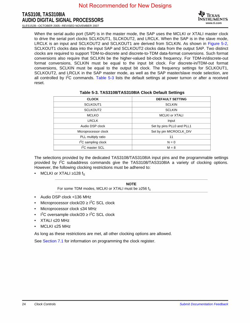
When the serial audio port (SAP) is in the master mode, the SAP uses the MCLKI or XTALI master clockto drive the serial port clocks SCLKOUT1, SLCKOUT2, and LRCLK. When the SAP is in the slave mode,LRCLK is an input and SCLKOUT2 and SCLKOUT1 are derived from SCLKIN. As shown in Figure 5-2,SCLKOUT1 clocks data into the input SAP and SCLKOUT2 clocks data from the output SAP. Two distinctclocks are required to support TDM-to-discrete and discrete-to-TDM data-format conversions. Such formatconversions also require that SCLKIN be the higher-valued bit-clock frequency. For TDM-in/discrete-outformat conversions, SCLKIN must be equal to the input bit clock. For discrete-in/TDM-out formatconversions, SCLKIN must be equal to the output bit clock. The frequency settings for SCLKOUT1,SCLKOUT2, and LRCLK in the SAP master mode, as well as the SAP master/slave mode selection, areall controlled by I2C commands. Table 5-3 lists the default settings at power turnon or after a receivedreset.
Audio DSP clock Set by pins PLL0 and PLL1Microprocessor clock Set by pin MICROCLK_DIV
PLL multiply ratio 11I2C sampling clock N = 0
I2C master SCL M = 8
The selections provided by the dedicated TAS3108/TAS3108IA input pins and the programmable settingsprovided by I2C subaddress commands give the TAS3108/TAS3108IA a variety of clocking options.However, the following clocking restrictions must be adhered to:• MCLKI or XTALI ≥128 fS
NOTEFor some TDM modes, MCLKI or XTALI must be ≥256 fS
The 8051 microprocessor receives and distributes I2C write data, retrieves and outputs to the I2C buscontrollers the required I2C read data, and participates in most processing tasks requiring multiframeprocessing cycles. The microprocessor has its own data RAM for storing intermediate values and queuingI2C commands, a fixed boot-program ROM, and a program RAM. The microprocessor boot programcannot be altered. The microprocessor controller has specialized hardware for master and slave interfaceoperation, volume updates, and a programmable interval timer interrupt. For more information, see theTAS3108/TAS3108IA Firmware Programmer's Guide (SLEU067).
The TAS3108/TAS3108IA has a slave-only I2C interface that is compatible with the inter-IC (I2C) busprotocol and supports both 100-kbps and 400-kbps data-transfer rates for multiple 4-byte write and readoperations (maximum is 20 bytes). The slave I2C control interface is used to program the registers of thedevice and to read device status.
The TAS3108/TAS3108IA also has a master-only I2C interface that is compatible with the I2C bus protocoland supports 375-kbps data transfer rates for multiple 4-byte write and read operations (maximum is 20bytes). The master I2C interface is used to load program and data from an external I2C EEPROM.
On power up of the TAS3108/TAS3108IA, the slave interface is disabled and the master interface isenabled. Following a reset, the TAS3108/TAS3108IA disables the slave interface and enables the masterinterface. Using the master interface, the TAS3108/TAS3108IA automatically tests to see if an I2CEEPROM is at address 1010xxx. The value xxx can be chip select, other information, or don’t cares,depending on the EEPROM selected. If a memory is present and it contains the correct headerinformation and one or more blocks of program/memory data, the TAS3108/TAS3108IA loads theprogram, coefficient, and/or data memories from the EEPROM. If a memory is present, the download iscomplete when a header is read that has a zero-length data segment. At this point, theTAS3108/TAS3108IA disables the master I2C interface, enables the slave I2C interface, and starts normaloperation.
If no memory is present or if an error occurred during the EEPROM read, TAS3108/TAS3108IA disablesthe master I2C interface, enables the slave I2C interface, and loads the unprogrammed defaultconfiguration. In this default configuration, the TAS3108/TAS3108IA streams eight channels of audio frominput to output if the GPIO pin is LOW. The master and slave interfaces do not operate simultaneously.
In the slave mode, the I2C bus is used to:• Load the program and coefficient data
– Microprocessor program memory– Microprocessor extended memory– Audio DSP core program memory– Audio DSP core coefficient memory– Audio DSP core data memory
• Update coefficient and other control values• Read status flags
Once the microprocessor program memory has been loaded, it cannot be updated until theTAS3108/TAS3108IA has been reset.
The master and slave modes do not operate simultaneously.
When acting as an I2C master, the data transfer rate is fixed at 375 kHz, assuming MCLKI orXTALI = 12.288 MHz, PLL0 = PLL1 = 0, and MICROCLK_DIV = 0.
When acting as an I2C slave, the data transfer rate is determined by the master device on the bus. TheI2C communication protocol for the I2C slave mode is shown in Figure 6-1.
TAS3108, TAS3108IAAUDIO DIGITAL SIGNAL PROCESSORSSLES152B–OCTOBER 2005–REVISED NOVEMBER 2007
Figure 6-1. I2C Slave-Mode Communication Protocol
As shown in Figure 6-2, an I2C read transaction requires that the master device first issue a writetransaction to give the TAS3108/TAS3108IA the subaddress to be used in the read transaction thatfollows. This subaddress assignment write transaction is then followed by the read transaction. For writetransactions, the subaddress is supplied in the first byte of data written, and this byte is followed by thedata to be written. For I2C write transactions, the subaddress must always be included in the data written.There cannot be a separate write transaction to supply the subaddress, as was required for readtransactions. If a subaddress assignment-only write transaction is followed by a second write transactionsupplying the data, erroneous behavior results. The first byte in the second write transaction is interpretedby the TAS3108/TAS3108IA as another subaddress replacing the one previously written.
The I2C slave mode is the mode that is used to change configuration parameters during operation and toperform program and coefficient downloads from a master device. The latter can be used to replace theI2C master-mode EEPROM download. The TAS3108/TAS3108IA supports both random and sequentialI2C transactions. The TAS3108/TAS3108IA I2C slave address is 011010xy, where the first six bits are theTAS3108/TAS3108IA device address and bit x is CS0, which is set by the TAS3108/TAS3108IA internalmicroprocessor at power up. Bit y is the R/W bit. The pulldown resistance of CS0 creates a default 00address when no connection is made to the pin. Table 6-1 and Table 6-2 show all the legal addresses forI2C slave and master modes.
The TAS3108/TAS3108IA I2C block does respond to the broadcast address (00h).
The following is an example use of the I2C master address to access an external EEPROM. TheTAS3108/TAS3108IA can address up to two EEPROMs depending on the state of CS0. Initially, theTAS3108/TAS3108IA comes up in I2C master mode. If it finds a memory such as the 24C512 EEPROM, itreads the headers and data as previously described. In this I2C master mode, the TAS3108/TAS3108IAaddresses the EEPROMs as shown in Table 6-3 and Table 6-4.
Supplying a subaddress for each subaddress transaction is referred to as random I2C addressing. Forrandom I2C read commands, the TAS3108/TAS3108IA responds with data, a byte at a time, starting at thesubaddress assigned, as long as the master device continues to respond with acknowledges. If a givensubaddress does not use all 32 bits, the unused bits are read as logic 0. I2C write commands, however,are treated in accordance with the data assignment for that address space. If a write command is receivedfor a biquad subaddress, for example, the TAS3108/TAS3108IA expects to see five 32-bit words. If fewerthan five data words have been received when a stop command (or another start command) is received,the data received is discarded.
Sequential I2C Transactions
The TAS3108/TAS3108IA also supports sequential I2C addressing. For write transactions, if a subaddressis issued followed by data for that subaddress and the 15 subaddresses that follow, a sequential I2C writetransaction has taken place, and the data for all 16 subaddresses is successfully received by theTAS3108/TAS3108IA. For I2C sequential write transactions, the subaddress then serves as the startaddress, and the amount of data subsequently transmitted before a stop or start is transmitted determineshow many subaddresses are written to. As was true for random addressing, sequential addressingrequires that a complete set of data be transmitted. If only a partial set of data is written to the lastsubaddress, the data for the last subaddress is discarded. However, all other data written is accepted; justthe incomplete data is discarded.
Sequential read transactions do not have restrictions on outputting only complete subaddress data sets.
If the master does not issue enough data-received acknowledges to receive all the data for a givensubaddress, the master device does not receive all the data.
If the master device issues more data-received acknowledges than required to receive the data for a givensubaddress, the master device simply receives complete or partial sets of data, depending on how manydata-received acknowledges are issued from the subaddress(es) that follow. I2C read transactions, bothsequential and random, can impose wait states.
For the standard I2C mode (SCL = 100 kHz), worst-case wait state time for an 8-MHz microprocessorclock is on the order of 2 µs. Nominal wait-state time for the same 8-MHz microprocessor clock is on theorder of 1 µs. For the fast I2C mode (SCL = 400 kHz) and the same 8-MHz microprocessor clock,worst-case wait-state time can extend up to 10.5 µs in duration. Nominal wait-state time for this samecase lies in a range from 2 µs to 4.6 µs. Increasing the microprocessor clock frequency lowers thewait-state time and for the standard I2C mode, a faster microprocessor clock can totally eliminate thepresence of wait states.
For example, increasing the microprocessor clock to 16 MHz results in no wait states. For the fast I2Cmode, faster microprocessor clocks shorten the wait-state time encountered, but do not totally eliminatewait states.
Multiple data bytes are transmitted by the master device to slave as shown in Figure 6-3. After receivingeach data byte, the TAS3108/TAS3108IA responds with an acknowledge bit.
Figure 6-3. Multiple-Byte Write Transfer
Multiple data bytes are transmitted by the TAS3108/TAS3108IA to the master device as shown inFigure 6-4. Except for the last data byte, the master device responds with an acknowledge bit afterreceiving each data byte.
Figure 6-4. Multiple-Byte Read Transfer
I2C master-mode operation is enabled following a reset or power-on reset. Master-mode I2C transactionsdo not start until the I2C bus is idle.
The TAS3108/TAS3108IA uses the master mode to download from EEPROM the memory contents for themicroprocessor program memory, microprocessor extended memory, audio DSP core program memory,audio DSP core coefficient memory, and audio DSP core data memory.
The TAS3108/TAS3108IA, when operating as an I2C master, can execute a complete download of anyinternal memory or any section of any internal memory without requiring any wait states.
TAS3108, TAS3108IAAUDIO DIGITAL SIGNAL PROCESSORSSLES152B–OCTOBER 2005–REVISED NOVEMBER 2007
When the TAS3108/TAS3108IA operates as an I2C master, the TAS3108/TAS3108IA generates arepeated start without an intervening stop command while downloading program and memory data fromEEPROM. When a repeated start is sent to the EEPROM in read mode, the EEPROM enters a sequentialread mode to transfer large blocks of data quickly.
The TAS3108/TAS3108IA queries the bus for an I2C EEPROM at address 1010xxx. The value xxx can bechip select, other information, or don’t cares, depending on the EEPROM selected.
The first action of the TAS3108/TAS3108IA as master is to transmit a start condition along with the deviceaddress of the I2C EEPROM with the read/write bit cleared (0) to indicate a write. The EEPROMacknowledges the address byte, and the TAS3108/TAS3108IA sends a subaddress byte, which theEEPROM acknowledges. Most EEPROMs have at least 2-byte addresses and acknowledge as many asare appropriate. At this point, the EEPROM sends a last acknowledge and becomes a slave transmitter.The TAS3108/TAS3108IA acknowledges each byte repeatedly to continue reading each data byte that isstored in memory.
The memory load information starts with reading the header and data information that starts atsubaddress 0 of the EEPROM. This information must then be stored in sequential memory addresses withno intervening gaps. The data blocks are contiguous blocks of data that immediately follow the headerlocations.
The TAS3108/TAS3108IA memory data can be stored and loaded in (almost) any order. Additionally, thisaddressing scheme permits portions of the TAS3108/TAS3108IA internal memories to be loaded.
Figure 6-5. EEPROM Address Map
The TAS3108/TAS3108IA sequentially reads EEPROM memory and loads its internal memory unless itdoes not find a valid memory header block, is not able to read the next memory location because the endof memory was reached, detects a checksum error, or reads an end-of-program header block. When itencounters an invalid header or read error, the TAS3108/TAS3108IA attempts to read the header ormemory location three times before it determines that it has an error. If the TAS3108/TAS3108IAencounters a checksum error it attempts to reread the entire block of memory two more times before itdetermines that it has an error.
Once the microprocessor program memory has been loaded, it cannot be reloaded until theTAS3108/TAS3108IA has been reset.
If an error is encountered, TAS3108/TAS3108IA terminates its memory-load operation, loads the defaultconfiguration, and disables further master I2C bus operations.
If an end-of-program data block is read, the TAS3108/TAS3108IA has completed the initial program load.
The I2C master mode uses the starting and ending I2C checksums to verify a proper EEPROM download.The first 16-bit data word received from the EEPROM, the I2C checksum at subaddress 0x00, is storedand compared against the 16-bit data word received for the last subaddress, the ending I2C checksum,and the checksum that is computed during the download. These three values must be equal. If the readand computed values do not match, the TAS3108/TAS3108IA sets the memory read error bits in thestatus register and repeats the download from the EEPROM two more times. If the comparison check failsthe third time, the TAS3108/TAS3108IA sets the microprocessor program to the default value.
Table 6-5 shows the format of the EEPROM or other external memory load file. Each line of the file is abyte (in ASCII format). The checksum is the summation of all the bytes (with beginning and endingchecksum fields = 00). The final checksum inserted into the checksum field is the lowest significant fourbytes of the checksum.
Example:
Given the following example 8051 data or program block (must be a multiple of 4 bytes for these blocks):
TAS3108, TAS3108IAAUDIO DIGITAL SIGNAL PROCESSORSSLES152B–OCTOBER 2005–REVISED NOVEMBER 2007
Table 6-5. TAS3108/TAS3108IA Memory Block StructuresSTARTING DATA BLOCK FORMAT SIZE NOTESBYTE
12-Byte Header Block0 Checksum code MS byte 2 bytes Checksum of bytes 2 through N + 12
Checksum code LS byte2 Header ID byte 1 = 0x00 2 bytes Must be 0x001F for the TAS3108/TAS3108IA to load
Header ID byte 2 = 0x1F4 Memory to be loaded 1 byte 0x00 Microprocessor program memory or termination
header0x01 Microprocessor external data memory0x02 Audio DSP core program memory0x03 Audio DSP core coefficient memory0x04 Audio DSP core data memory0x05–0x0F Reserved for future expansion
5 0x00 1 byte Unused6 Start TAS3108/TAS3108IA memory address MS 2 bytes If this is a termination header, this value is 0000.
byteStart TAS3108/TAS3108IA memory address LS byte
8 Total number of bytes transferred MS byte 2 bytes 12 + data bytes + last checksum bytes. If this is atermination header, this value is 0000.Total number of bytes transferred LS byte
10 0x00 1 bytes Unused11 0x00 1 bytes Unused
Data Block for Microprocessor Program or Data Memory (Following 12-Byte Header)12 Data byte 1 (LS byte) 4 bytes 1–4 microprocessor bytes
Data byte 2Data byte 3
Data byte 4 (MS byte)16 Data byte 5 4 bytes 5–8 microprocessor bytes
Data byte 4*(Z – 1) + 4 = NN + 12 0x00 4 bytes Repeated checksum bytes 2 through N + 11
0x00Checksum code MS byteChecksum code LS byte
Data Block for Audio DSP Core Coefficient Memory (Following 12-Byte Header)12 Data byte 1 (LS byte) 4 bytes Coefficient word 1 (valid data in D27–D0) D7–D0
TAS3108, TAS3108IAAUDIO DIGITAL SIGNAL PROCESSORSSLES152B–OCTOBER 2005–REVISED NOVEMBER 2007
Register 0x00 provides the user with control over MCLK, LRCLK, SCLKOUT1, SCLKOUT2, data-wordsize, and serial audio port modes. Register 0x00 default = 0x0100 1B22.
IMS SAP master/slave mux select (1 = master mode, 0 = slave mode)X2 X1 X0 SCLKIN and SCLKOUT clock divide
Z2 Z1 Z0 MCLK, SCLK ratio (master mode only)
D15 D14 D13 D12 D11 D10 D9 D8 DESCRIPTIONX X Don't care
X Don't careIW1 IW0 Input audio data word size
X Don't careOW1 OW0 Output audio data word size
D7 D6 D5 D4 D3 D2 D1 D0 DESCRIPTIONIM3 IM2 IM1 IM0 Input data format
OM3 OM2 OM1 OM0 Output data format
Bits 28–27 (W1 and W0) define the ratio between MCLKI (or the crystal frequency) and MCLKO. Thisallows the accommodation of devices that require an MCLK = 128 LRCLK and devices that require anMCLK = 256 LRCLK, without having to use glue logic to divide that clock down. This bit has meaningwhether in clock-master or clock-slave mode.
Bits 26–24 (Y2, Y1, and Y0) define the ratio between SCLK and LRCLK, but only have meaning in theclock-master mode where LRCLK is an output. In the clock-slave mode, LRCLK is an input.
Y2 Y1 Y0 DESCRIPTION0 0 0 LRCLK out = SCLK/320 0 1 LRCLK out = SCLK/640 1 0 LRCLK out = SCLK/1280 1 1 LRCLK out = SCLK/1921 0 0 LRCLK out = SCLK/2561 0 1 LRCLK out = SCLK/3841 1 0 LRCLK out = SCLK/5121 1 1 LRCLK out = SCLK/32
Bits 21–19 (X2, X1, and X0) define the ratio between SCLKIN and SCLKOUT. These control bits are onlyused when the input and output rates are different, which can happen if TDM and discrete modes are bothused (for example, input is TDM and output is discrete). Normally, these bits are set to 000, so thatSCLKOUT1 (input SCLK) and SLCKOUT2 (output SCLK) are the same. (Note that SCLKIN is not theinput SCLK, but is used in clock-slave mode to derive SCLKOUT1.)
X2 X1 X0 DESCRIPTION0 0 0 X MUX out = IMS_MUX (master/slave SCLK)0 0 1 X MUX out = IMS_MUX/20 1 0 X MUX out = IMS_MUX/30 1 1 X MUX out = IMS_MUX/41 0 0 X MUX out = IMS_MUX/61 0 1 X MUX out = IMS_MUX/81 1 0 X MUX out = IMS_MUX/161 1 1 X MUX out = IMS_MUX/32
Bits 18–16 (Z2, Z1, and Z0) define the ratio between MCLK and SCLK when the TAS3108/TAS3108IA isthe clock master. In clock-slave mode, these bits are don't care.
Z2 Z1 Z0 DESCRIPTION0 0 0 Z MUX out = MCLK (MCLKI or crystal oscillator)0 0 1 Z MUX out = MCLK/20 1 0 Z MUX out = MCLK/30 1 1 Z MUX out = MCLK/41 0 0 Z MUX out = MCLK/61 0 1 Z MUX out = MCLK/81 1 0 Z MUX out = MCLK/161 1 1 Z MUX out = MCLK/32
Bits 7–4 (IM3, IM2, IM1, and IM0) define the input data format. Bits 3–0 (OM3, OM2, OM1, and OM0)define the output data format. The two formats need not be the same, only compatible.
During I2C download, the write operation to indicate that a particular memory is to be written causes theTAS3108/TAS3108IA to set an error bit to indicate a load for that memory type. This error bit is clearedwhen the operation completes successfully.
7.3 I2C Memory Load Control and Data Registers (0x04 and 0x05)
TAS3108, TAS3108IAAUDIO DIGITAL SIGNAL PROCESSORSSLES152B–OCTOBER 2005–REVISED NOVEMBER 2007
Registers 0x04 (Table 7-3) and 0x05 (Table 7-4) allow the user to download TAS3108/TAS3108IAprogram code and data directly from the system I2C controller. This mode is called the I2C slave mode(from the TAS3108/TAS3108IA point-of-view). See the TAS3108/TAS3108IA Firmware Programmer'sGuide (SLEU067) for more details.
Table 7-3. TAS3108/TAS3108IA Memory Load Control Register (0x04)BYTE DATA BLOCK FORMAT SIZE NOTES1–2 Checksum code 2 bytes Checksum of bytes 2 through N + 8. If this is a termination header,
this value is 0000.3–4 Memory to be loaded 2 bytes 0 Microprocessor program memory
1 Microprocessor external data memory2 Audio DSP core program memory3 Audio DSP core coefficient memory4 Audio DSP core data memory5–15 Reserved for future expansion
5 Unused 1 byte Reserved for future expansion6–7 Starting TAS3108/TAS3108IA memory 2 bytes If this is a termination header – this value is 0000.
address7–8 Number of data bytes to be transferred 2 bytes If this is a termination header – this value is 0000.
Table 7-4. TAS3108/TAS3108IA Memory Load Data Register (0x05)BYTE 8-BIT DATA 28-BIT DATA 48-BIT DATA 54-BIT DATA
1 Datum 1 D7–D0 0000 D27–D24 0000 0000 0000 00002 Datum 2 D7–D0 D7–D0 0000 0000 00 D53–D483 Datum 3 D7–D0 D15–D8 D47–D40 D47–D404 Datum 4 D7–D0 D7–D0 D39–D32 D39–D325 Datum 5 D7–D0 0000 D27–D24 D31–D24 D31–D246 Datum 6 D7–D0 D23–D16 D23–D16 D23–D167 Datum 7 D7–D0 D15–D8 D15–D8 D15–D88 Datum 8 D7–D0 D7–D0 D7–D0 D7–D0
Registers 0x06 (Table 7-5) and 0x07 (Table 7-6) allow the user to access the internal resources of theTAS3108/TAS3108IA. See TAS3108/TAS3108IA Firmware Programmer's Guide (SLEU067) for moredetails.
TAS3108, TAS3108IAAUDIO DIGITAL SIGNAL PROCESSORSSLES152B–OCTOBER 2005–REVISED NOVEMBER 2007
Supply voltage range, DVDD –0.5 V to 3.8 VSupply voltage, AVDD –0.5 V to 3.8 V
3.3-V TTL –0.5 V to DVDD + 0.5 VInput voltageVI range 1.8 V LVCMOS (XTLI) –0.5 V to 2.3 V3.3 V TTL –0.5 V to DVDD + 0.5 VOutput voltageVO range 1.8 V LVCMOS (XTLO) –0.5 V to 2.3V (2)
IIK Input clamp current (VI < 0 or VI > DVDD ±20 µAIOK Output clamp current (VO < 0 or VO > DVDD) ±20 µA
TAS3108 operating free-air temperature 0°C to 70°CTA TAS3108IA operating free-air temperature –40°C to 105°CTstg Storage temperature range –65°C to 150°C
(1) Stresses beyond those listed under "absolute maximum ratings" may cause permanent damage to the device. These are stress ratingsonly, and functional operation of the device at these or any other conditions beyond those indicated under "recommended operatingconditions" is not implied. Exposure to absolute-maximum-rated conditions for extended periods may affect device reliability.
(2) Pin XTALO is the only TAS3108/TAS3108IA output that is derived from the internal 1.8-V logic supply. The absolute maximum ratinglisted is for reference; only a crystal should be connected to XTALO.
TAS3108, TAS3108IAAUDIO DIGITAL SIGNAL PROCESSORSSLES152B–OCTOBER 2005–REVISED NOVEMBER 2007
The following sections describe the timing characteristics of the TAS3108/TAS3108IA.
over recommended operating conditions (unless otherwise noted)
TESTPARAMETER MIN TYP MAX UNITCONDITIONSf(XTALI) Frequency, XTALI (1/ tc(1)) See (1) 6 (2) 20 (2) MHztc(1) Cycle time, XTALI 50 (2) 166 (2) nsf(MCLKI) Frequency, MCLKI (1/ tc(2)) 6 (2) 25 MHztw(MCLKI) Pulse duration, MCLKI high See (3) 0.4 tc(2) 0.5 tc(2) 0.6 tc(2) ns
MCLKI jitter ±5 (2) nsf(MCLKO) Frequency, MCLKO (1/ tc(3)) 6 (2) 25 (2) MHztr(MCLKO) Rise time, MCLKO CL = 30 pF 15 (2) nstf(MCLKO) Fall time, MCLKO CL = 30 pF 15 (2) nstw(MCLKO) Pulse duration, MCLKO high See (4) HMCLKO ns
XTALI master clock source 80MCLKO jitter ps
MCLKI master clock source See (5)
Delay time, MCLKI rising MCLKO = MCLKI See (6) 20 (2)
td(MI-MO) edge to MCLKO rising nsMCLKO < MCLKI See (6) (7) 20 (2)
edge
(1) Duty cycle is 50/50.(2) This measurement is specified by design.(3) Period of MCLKI = TMCLKI = 1 / fMCLKI(4) HMCLKO = 1/(2 × MCLKO). MCLKO has the same duty cycle as MCLKI when MCLKO = MCLKI. When MCLKO = 0.5 MCLKI or 0.25
MCLKI, the duty cycle of MCLKO is typically 50%.(5) When MCLKO is derived from MCLKI, MCLKO jitter = MCLKI jitter(6) Only applies when MCLKI is selected as master source clock(7) Also applies to MCLKO falling edge when MCLKO = MCLKI/2 or MCLKI/4.
8.5.4 Pin-Related Characteristics of the SDA and SCL I/O Stages for F/S-Mode I2C-Bus Devices
TAS3108, TAS3108IAAUDIO DIGITAL SIGNAL PROCESSORS
SLES152B–OCTOBER 2005–REVISED NOVEMBER 2007
STANDARD MODE FAST MODEPARAMETER TEST CONDITIONS UNIT
MIN MAX MIN MAXVIL LOW-level input voltage –0.5 (1) 0.8 –0.5 (1) 0.8 VVIH HIGH-level input voltage 2 2 VVhys Hysteresis of inputs N/A N/A 0.05 VDD
(1) VLOW-level output voltage (open drain orVOL1 3-mA sink current 0 0.4 (1) Vopen collector)
Bus capacitance from 10 pF 7 + 0.1 Cbtof Output fall time from VIHmin to VILmax 250 (1) 250 (1) nsto 400 pF (2) (1)
II Input current, each I/O pin –10 10 –10 (3) 10 (3) µASCL pulse duration of spikes that musttSP(SCL) N/A N/A 14 (4) (1) nsbe suppressed by the input filterSDA pulse duration of spikes that musttSP(SDA) N/A N/A 22 (4) (1) nsbe suppressed by the input filter
CI Capacitance, each I/O pin 10 (1) 10 (1) pF
(1) This measurement in specified by design.(2) Cb = capacitance of one bus line in pF. The output fall time is faster than the standard I2C specification.(3) The I/O pins of fast-mode devices must not obstruct the SDA and SDL lines if VDD is switched off.(4) These values are valid at the 135-MHz DSP clock rate. If DSP clock is reduced by one half, the tSP doubles.
NOTESDA does not have the standard I2C specification 300-ns internal hold time. SDA must bevalid by the rising and falling edges of SCL.
8.5.5 Bus-Related Characteristics of the SDA and SCL I/O Stages for F/S-Mode I2C-Bus
SDA
SCL
tf tSU-DAT tHD-STA tr
tBUF
tSU-STO
P S
tSP
tSU-STA
Sr
tHIGH
tHD-DAT
tLOW
tr
tHD-STA
S
tf
T0114-01
TAS3108, TAS3108IAAUDIO DIGITAL SIGNAL PROCESSORSSLES152B–OCTOBER 2005–REVISED NOVEMBER 2007
DevicesAll values are referred to VIHmin and VILmax (see Section 8.5.4).
A
STANDARD MODE FAST MODETESTPARAMETER UNITCONDITIONS MIN MAX MIN MAXfSCL SCL clock frequency (1) 0 (1) 100 0 (1) 400 (2) kHz
Hold time (repeated) START condition.tHD-STA After this period, the first clock pulse is 4 (1) 0.6 (1) µs
generated.tLOW LOW period of the SCL clock 4.7 (1) 1.3 (1) µstHIGH HIGH period of the SCL clock 4 (1) 0.6 (1) µstSU-STA Setup time for repeated START 4.7 (1) 0.6 (1) µstSU-DAT Data setup time 250 (1) 100 (1) nstHD-DAT Data hold time (3) (4) 0 (1) 3.45 (1) 0 (1) 0.9 (1) µs
20 + 0.1tr Rise time of both SDA and SCL signals 1000 (1) 300 (1) nsCb(5) (1)
20 + 0.1tf Fall time of both SDA and SCL 300 (1) 300 (1) nsCb(5) (1)
tSU-STO Setup time for STOP condition 4 (1) 0.6 (1) µsBus free time between a STOP andtBUF 4.7 (1) 1.3 (1) µsSTART condition
Cb Capacitive load for each bus line 400 (1) 400 (1) pFNoise margin at the LOW level for eachVnL 0.1 VDVDD
Noise margin at the HIGH level for eachVnH 0.2 VDVDD(1) 0.2 VDVDD
(1) Vconnected device (including hysteresis)
(1) This measurement is specified by design.(2) In master mode, the maximum speed is 375 kHz.(3) Note that SDA does not have the standard I2C specification 300-ns internal hold time. SDA must be valid by the rising and falling edges
of SCL. TI recommends that a 2-kΩ pullup resistor be used to avoid potential timing issues.(4) A fast-mode I2C-bus device can be used in a standard-mode I2C-bus system, but the requirement tSU-DAT ≥ 250 ns must then be met.
This is automatically the case if the device does not stretch the LOW period of the SCL signal. If such a device does stretch the LOWperiod of the SCL signal, it must output the next data bit to the SDA line tr-max + tSU-DAT = 1000 + 250 = 1250 ns (according to thestandard-mode I2C bus specification) before the SCL line is released.
(5) Cb = total capacitance of one bus line in pF.
Figure 8-4. Start and Stop Conditions Timing Waveforms
It is recommended that the I2C pullup resistors RP be 4.7 kΩ (see Figure 8-5). If a series resistor is in thecircuit (see Figure 8-6), then the series resistor RS should be less than or equal to 300 Ω.
Figure 8-5. I2C Pullup Circuit (With No Series Resistor)
(1) VS = DVDD × RS/S = RP). When driven low, VS << VIL requirements.(2) RS ≤ 300 Ω
Figure 8-6. I2C Pullup Circuit (With Series Resistor)
control signal parameters over recommended operating conditions; these measurements are specified by design (unlessotherwise noted)
PARAMETER TEST CONDITIONS MIN MAX UNITtw(RESET) Pulse duration, RESET active 10 (1) nstr(run) Time to enable I2C PLL0 = PLL1 = MICROCLK_DIV = 0 10 (1) ms
Figure 9-1 shows a typical TAS3108/TAS3108IA application. In this application, the following conditionsapply:
• TAS3108/TAS3108IA is in clock-slave mode. The audio (SDIN1, SDIN2, SDIN3, SDIN4) and clocksource (MCLKI) are external.
• MCLKI = 12.288 MHz• Because MCLKI is sourced externally, the TAS3108/TAS3108IA crystal interface is not used. MCLKI
and XTLI are logically ORed together, meaning that when the MCLKI pin is used, the XTALI pin mustbe grounded.
• I2C register 0x00 contains the default settings which means:– Audio data word size is 24-bit input and 24-bit output.– Serial data format is 2 channel, I2S for input and output.– I2C data transfer is approximately 400 kbps for both master and slave I2C interfaces.– PLL0 = PLL1 = PLL2 = 0 means that fDSPCLK is 11 × MCLKI = 135.2 MHz and that
fI2CSCL = 375 kHz.– Sample frequency (fS) is 48 kHz, which requires that fLRCLK = 48 kHz and fSCLKIN = 3.072 MHz.
• Application code and data are loaded from an external EEPROM using the master I2C interface.• Application commands come from the system microprocessor to the TAS3108/TAS3108IA using the
slave I2C interface.
Good design practice requires isolation between the digital and analog power as shown. Power-supplycapacitors of 10 µF and 0.1 µF should be placed near the power-supply pins AVDD (AVSS) and DVDD(DVSS).
The TAS3108/TAS3108IA reset needs external glitch protection. Also, reset going HIGH should bedelayed until TAS3108/TAS3108IA internal power is good (~200 µs). This is provided by the 1-kΩ resistor,1-µF capacitor, and diode placed near the RESET pin.
It is recommended that a 4.7-µF capacitor (fast ceramic type) be placed near pin 28 (VR_DIG). This pinmust not be used to source external components.
Submit Documentation Feedback Application Information 53
9.3 Recommended PCB Design for TAS3108IA Applications
TAS3108, TAS3108IAAUDIO DIGITAL SIGNAL PROCESSORS
SLES152B–OCTOBER 2005–REVISED NOVEMBER 2007
• MCLKI and XTLI are logically ORed together, meaning that when the XTALI pin is used, the MCLKI pinmust be grounded.
• Crystal type = Parallel-mode, fundamental-mode crystal• rd = Drive-level control resistor – vendor specified• CL = Crystal load capacitance (capacitance of circuitry between the two terminals of the crystal)• CL = (C1 × C2)/C1 + C2) + CS (where CS = board stray capacitance, ~2 pF)
Automotive applications require that the TAS3108IA operates properly while in an ambient temperaturerange of –40° C to 105°C. Under the high-temperature condition of 105°C ambient, the TAS3108IAthermal pad must be soldered to a copper area on the PCB designed for thermal relief.
High-temperature applications also require that the application be built on a high-K dielectric PCB.
High-K dielectric PCB requirements for using TAS3108IA with soldered thermal pad:• 0.062 in thick• Minimum 3-in × 3-in PCB• 2-oz copper traces located on top of the board (0,071 mm thick)• Copper area located on the top and bottom of the PCB for soldering• Power and ground planes, 1-oz. copper (0,036 mm thick)• Thermal vias, 0.3-mm diameter, 1.5-mm pitch• Thermal isolation of power plane
If the target application limits the ambient temperature to 0°C to 70°C (standard commercialtemperature range), the thermal pad does not need to be soldered to the PCB.
For more information, see PowerPAD™ Thermally Enhanced Package (SLMA002) and PowerPADTM
Made Easy (SLMA004).
Submit Documentation Feedback Application Information 55
TAS3108DCP ACTIVE HTSSOP DCP 38 50 Green (RoHS& no Sb/Br)
CU NIPDAU Level-3-260C-168 HR 0 to 70 TAS3108
TAS3108DCPG4 ACTIVE HTSSOP DCP 38 50 Green (RoHS& no Sb/Br)
CU NIPDAU Level-3-260C-168 HR 0 to 70 TAS3108
TAS3108DCPR ACTIVE HTSSOP DCP 38 2000 Green (RoHS& no Sb/Br)
CU NIPDAU Level-3-260C-168 HR 0 to 70 TAS3108
TAS3108IADCP NRND HTSSOP DCP 38 50 Green (RoHS& no Sb/Br)
CU NIPDAU Level-3-260C-168 HR -40 to 105 TAS3108IA
TAS3108IADCPG4 NRND HTSSOP DCP 38 50 Green (RoHS& no Sb/Br)
CU NIPDAU Level-3-260C-168 HR -40 to 105 TAS3108IA
TAS3108IADCPR ACTIVE HTSSOP DCP 38 2000 Green (RoHS& no Sb/Br)
CU NIPDAU Level-3-260C-168 HR 0 to 0 TAS3108IA
TAS3108IADCPRG4 ACTIVE HTSSOP DCP 38 2000 Green (RoHS& no Sb/Br)
CU NIPDAU Level-3-260C-168 HR 0 to 0 TAS3108IA
(1) The marketing status values are defined as follows:ACTIVE: Product device recommended for new designs.LIFEBUY: TI has announced that the device will be discontinued, and a lifetime-buy period is in effect.NRND: Not recommended for new designs. Device is in production to support existing customers, but TI does not recommend using this part in a new design.PREVIEW: Device has been announced but is not in production. Samples may or may not be available.OBSOLETE: TI has discontinued the production of the device.
(2) RoHS: TI defines "RoHS" to mean semiconductor products that are compliant with the current EU RoHS requirements for all 10 RoHS substances, including the requirement that RoHS substancedo not exceed 0.1% by weight in homogeneous materials. Where designed to be soldered at high temperatures, "RoHS" products are suitable for use in specified lead-free processes. TI mayreference these types of products as "Pb-Free".RoHS Exempt: TI defines "RoHS Exempt" to mean products that contain lead but are compliant with EU RoHS pursuant to a specific EU RoHS exemption.Green: TI defines "Green" to mean the content of Chlorine (Cl) and Bromine (Br) based flame retardants meet JS709B low halogen requirements of <=1000ppm threshold. Antimony trioxide basedflame retardants must also meet the <=1000ppm threshold requirement.
(3) MSL, Peak Temp. - The Moisture Sensitivity Level rating according to the JEDEC industry standard classifications, and peak solder temperature.
(4) There may be additional marking, which relates to the logo, the lot trace code information, or the environmental category on the device.
(5) Multiple Device Markings will be inside parentheses. Only one Device Marking contained in parentheses and separated by a "~" will appear on a device. If a line is indented then it is a continuationof the previous line and the two combined represent the entire Device Marking for that device.
(6) Lead/Ball Finish - Orderable Devices may have multiple material finish options. Finish options are separated by a vertical ruled line. Lead/Ball Finish values may wrap to two lines if the finishvalue exceeds the maximum column width.
Important Information and Disclaimer:The information provided on this page represents TI's knowledge and belief as of the date that it is provided. TI bases its knowledge and belief on informationprovided by third parties, and makes no representation or warranty as to the accuracy of such information. Efforts are underway to better integrate information from third parties. TI has taken andcontinues to take reasonable steps to provide representative and accurate information but may not have conducted destructive testing or chemical analysis on incoming materials and chemicals.TI and TI suppliers consider certain information to be proprietary, and thus CAS numbers and other limited information may not be available for release.
In no event shall TI's liability arising out of such information exceed the total purchase price of the TI part(s) at issue in this document sold by TI to Customer on an annual basis.
Texas Instruments Incorporated (TI) reserves the right to make corrections, enhancements, improvements and other changes to itssemiconductor products and services per JESD46, latest issue, and to discontinue any product or service per JESD48, latest issue. Buyersshould obtain the latest relevant information before placing orders and should verify that such information is current and complete.TI’s published terms of sale for semiconductor products (http://www.ti.com/sc/docs/stdterms.htm) apply to the sale of packaged integratedcircuit products that TI has qualified and released to market. Additional terms may apply to the use or sale of other types of TI products andservices.Reproduction of significant portions of TI information in TI data sheets is permissible only if reproduction is without alteration and isaccompanied by all associated warranties, conditions, limitations, and notices. TI is not responsible or liable for such reproduceddocumentation. Information of third parties may be subject to additional restrictions. Resale of TI products or services with statementsdifferent from or beyond the parameters stated by TI for that product or service voids all express and any implied warranties for theassociated TI product or service and is an unfair and deceptive business practice. TI is not responsible or liable for any such statements.Buyers and others who are developing systems that incorporate TI products (collectively, “Designers”) understand and agree that Designersremain responsible for using their independent analysis, evaluation and judgment in designing their applications and that Designers havefull and exclusive responsibility to assure the safety of Designers' applications and compliance of their applications (and of all TI productsused in or for Designers’ applications) with all applicable regulations, laws and other applicable requirements. Designer represents that, withrespect to their applications, Designer has all the necessary expertise to create and implement safeguards that (1) anticipate dangerousconsequences of failures, (2) monitor failures and their consequences, and (3) lessen the likelihood of failures that might cause harm andtake appropriate actions. Designer agrees that prior to using or distributing any applications that include TI products, Designer willthoroughly test such applications and the functionality of such TI products as used in such applications.TI’s provision of technical, application or other design advice, quality characterization, reliability data or other services or information,including, but not limited to, reference designs and materials relating to evaluation modules, (collectively, “TI Resources”) are intended toassist designers who are developing applications that incorporate TI products; by downloading, accessing or using TI Resources in anyway, Designer (individually or, if Designer is acting on behalf of a company, Designer’s company) agrees to use any particular TI Resourcesolely for this purpose and subject to the terms of this Notice.TI’s provision of TI Resources does not expand or otherwise alter TI’s applicable published warranties or warranty disclaimers for TIproducts, and no additional obligations or liabilities arise from TI providing such TI Resources. TI reserves the right to make corrections,enhancements, improvements and other changes to its TI Resources. TI has not conducted any testing other than that specificallydescribed in the published documentation for a particular TI Resource.Designer is authorized to use, copy and modify any individual TI Resource only in connection with the development of applications thatinclude the TI product(s) identified in such TI Resource. NO OTHER LICENSE, EXPRESS OR IMPLIED, BY ESTOPPEL OR OTHERWISETO ANY OTHER TI INTELLECTUAL PROPERTY RIGHT, AND NO LICENSE TO ANY TECHNOLOGY OR INTELLECTUAL PROPERTYRIGHT OF TI OR ANY THIRD PARTY IS GRANTED HEREIN, including but not limited to any patent right, copyright, mask work right, orother intellectual property right relating to any combination, machine, or process in which TI products or services are used. Informationregarding or referencing third-party products or services does not constitute a license to use such products or services, or a warranty orendorsement thereof. Use of TI Resources may require a license from a third party under the patents or other intellectual property of thethird party, or a license from TI under the patents or other intellectual property of TI.TI RESOURCES ARE PROVIDED “AS IS” AND WITH ALL FAULTS. TI DISCLAIMS ALL OTHER WARRANTIES ORREPRESENTATIONS, EXPRESS OR IMPLIED, REGARDING RESOURCES OR USE THEREOF, INCLUDING BUT NOT LIMITED TOACCURACY OR COMPLETENESS, TITLE, ANY EPIDEMIC FAILURE WARRANTY AND ANY IMPLIED WARRANTIES OFMERCHANTABILITY, FITNESS FOR A PARTICULAR PURPOSE, AND NON-INFRINGEMENT OF ANY THIRD PARTY INTELLECTUALPROPERTY RIGHTS. TI SHALL NOT BE LIABLE FOR AND SHALL NOT DEFEND OR INDEMNIFY DESIGNER AGAINST ANY CLAIM,INCLUDING BUT NOT LIMITED TO ANY INFRINGEMENT CLAIM THAT RELATES TO OR IS BASED ON ANY COMBINATION OFPRODUCTS EVEN IF DESCRIBED IN TI RESOURCES OR OTHERWISE. IN NO EVENT SHALL TI BE LIABLE FOR ANY ACTUAL,DIRECT, SPECIAL, COLLATERAL, INDIRECT, PUNITIVE, INCIDENTAL, CONSEQUENTIAL OR EXEMPLARY DAMAGES INCONNECTION WITH OR ARISING OUT OF TI RESOURCES OR USE THEREOF, AND REGARDLESS OF WHETHER TI HAS BEENADVISED OF THE POSSIBILITY OF SUCH DAMAGES.Unless TI has explicitly designated an individual product as meeting the requirements of a particular industry standard (e.g., ISO/TS 16949and ISO 26262), TI is not responsible for any failure to meet such industry standard requirements.Where TI specifically promotes products as facilitating functional safety or as compliant with industry functional safety standards, suchproducts are intended to help enable customers to design and create their own applications that meet applicable functional safety standardsand requirements. Using products in an application does not by itself establish any safety features in the application. Designers mustensure compliance with safety-related requirements and standards applicable to their applications. Designer may not use any TI products inlife-critical medical equipment unless authorized officers of the parties have executed a special contract specifically governing such use.Life-critical medical equipment is medical equipment where failure of such equipment would cause serious bodily injury or death (e.g., lifesupport, pacemakers, defibrillators, heart pumps, neurostimulators, and implantables). Such equipment includes, without limitation, allmedical devices identified by the U.S. Food and Drug Administration as Class III devices and equivalent classifications outside the U.S.TI may expressly designate certain products as completing a particular qualification (e.g., Q100, Military Grade, or Enhanced Product).Designers agree that it has the necessary expertise to select the product with the appropriate qualification designation for their applicationsand that proper product selection is at Designers’ own risk. Designers are solely responsible for compliance with all legal and regulatoryrequirements in connection with such selection.Designer will fully indemnify TI and its representatives against any damages, costs, losses, and/or liabilities arising out of Designer’s non-compliance with the terms and provisions of this Notice.


![Approximation Algorithms and Hardness of the -Route Cut ...yuanz.web.illinois.edu/papers/kroute-soda.pdflem. The O(log2 nlogr)-approximation of [CK08], and the O(log2 r)-approximation](https://static.documents.pub/doc/80x56/5f533812733a1e1e8b10d92a/approximation-algorithms-and-hardness-of-the-route-cut-yuanzweb-lem-the-olog2.jpg)


