Note 3. Film synthesis [References] http:// home.agh.edu.pl/~scootmo http://ece.uwaterloo.ca/~bcui/ Google search Polycrystalline target Process of film synthesis Films on a substrate Source materials
Silicon wafer Thin film of Si or metal. Thin film of SiO2 or Si3N4.
Amorphous
• Polycrystalline means that the material is made of densely packed crystallites or grains of single crystal. Each grain has a more or less random orientation. The interface between crystallites is called a grain boundary.
• An amorphous material has no atomic or molecular ordering to speak of.
• Silicon wafers and epitaxial films are single crystalline as do high-quality gemstones such as ruby and sapphire (Al2O3 with impurities that produce the characteristic colors) as well as diamond.
Comparison of film deposition technologies
8
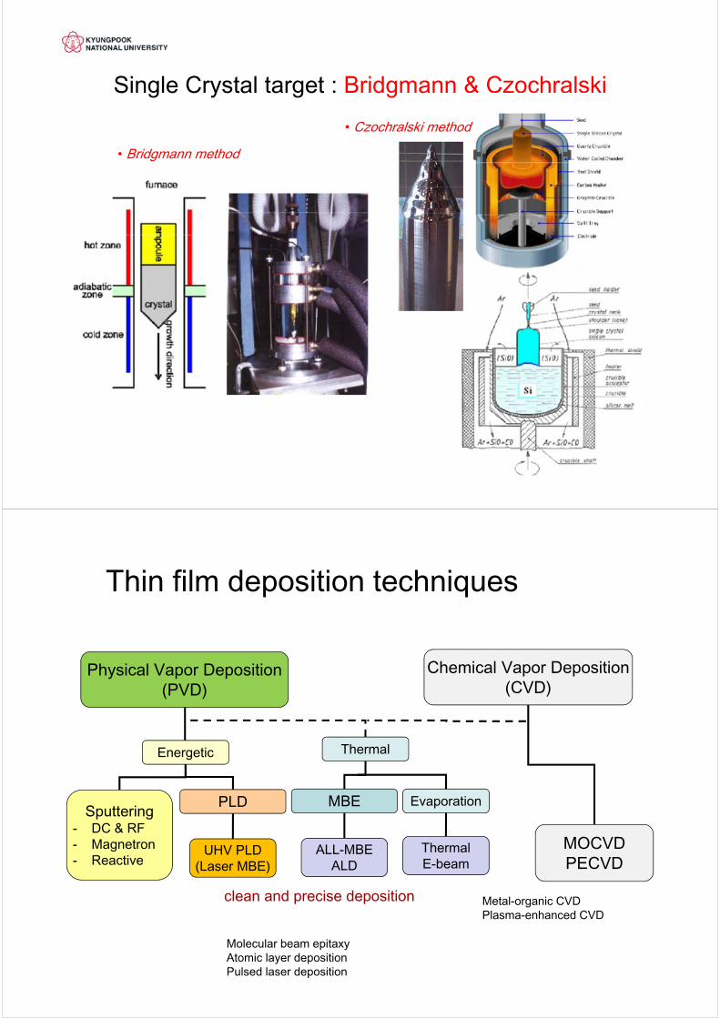
Evaporation• The source material is evaporated in a vacuum. The vacuum allows vapor
particles to travel directly to the target object (substrate), where they condense back to a solid state.
• In high vacuum, evaporated particles can travel directly to the deposition target without colliding with the background gas. At a typical pressure of 10−4 Pa, an 0.4-nm particle has a mean free path of 60 m. Hot objects in the evaporation chamber, such as heating filaments, produce unwanted vapors that limit the quality of the vacuum.
Evaporation
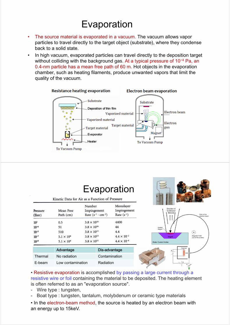
Advantage Dis-advantageThermal No radiation ContaminationE-beam Low contamination Radiation
• Resistive evaporation is accomplished by passing a large current through a resistive wire or foil containing the material to be deposited. The heating element is often referred to as an "evaporation source". - Wire type : tungsten, - Boat type : tungsten, tantalum, molybdenum or ceramic type materials
• In the electron-beam method, the source is heated by an electron beam with an energy up to 15keV.
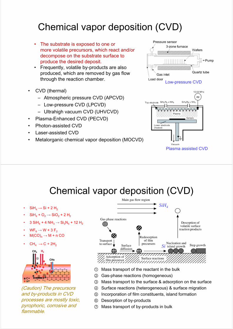
• The substrate is exposed to one or more volatile precursors, which react and/or decompose on the substrate surface to produce the desired deposit.
• Frequently, volatile by-products are also produced, which are removed by gas flow through the reaction chamber.
Chemical vapor deposition (CVD)SiH4
Si
① Mass transport of the reactant in the bulk② Gas-phase reactions (homogeneous)③ Mass transport to the surface & adsorption on the surface④ Surface reactions (heterogeneous) & surface migration⑤ Incorporation of film constituents, island formation⑥ Desorption of by-products⑦ Mass transport of by-products in bulk
• 3 SiH4 + 4 NH3 → Si3N4 + 12 H2
• SiH4 → Si + 2 H2
• SiH4 + O2 → SiO2 + 2 H2
• WF6 → W + 3 F2
• M(CO)n → M + n CO
• CH4 → C + 2H2
(Caution) The precursors and by-products in CVD processes are mostly toxic, pyrophoric, corrosive and flammable.
Molecular Beam Epitaxy (MBE)
ALD
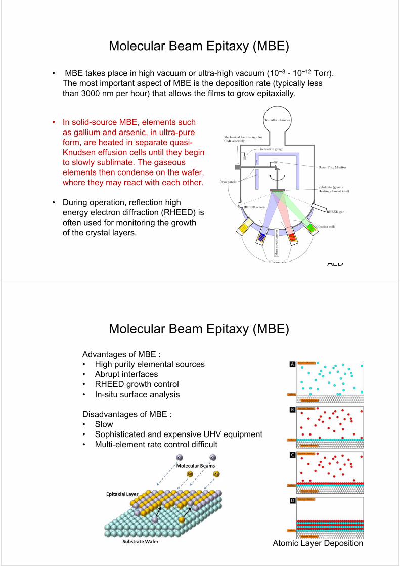
• MBE takes place in high vacuum or ultra-high vacuum (10−8 - 10−12 Torr). The most important aspect of MBE is the deposition rate (typically less than 3000 nm per hour) that allows the films to grow epitaxially.
• In solid-source MBE, elements such as gallium and arsenic, in ultra-pure form, are heated in separate quasi-Knudsen effusion cells until they begin to slowly sublimate. The gaseous elements then condense on the wafer, where they may react with each other.
• During operation, reflection high energy electron diffraction (RHEED) is often used for monitoring the growth of the crystal layers.
Advantages of MBE :• High purity elemental sources• Abrupt interfaces • RHEED growth control • In-situ surface analysis
Disadvantages of MBE : • Slow• Sophisticated and expensive UHV equipment• Multi-element rate control difficult
Molecular Beam Epitaxy (MBE)
Atomic Layer Deposition
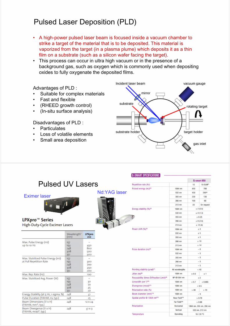
Advantages of PLD :• Suitable for complex materials • Fast and flexible• (RHEED growth control) • (In-situ surface analysis)
Disadvantages of PLD : • Particulates• Loss of volatile elements• Small area deposition
Pulsed Laser Deposition (PLD)
• A high-power pulsed laser beam is focused inside a vacuum chamber to strike a target of the material that is to be deposited. This material is vaporized from the target (in a plasma plume) which deposits it as a thin film on a substrate (such as a silicon wafer facing the target).
• This process can occur in ultra high vacuum or in the presence of a background gas, such as oxygen which is commonly used when depositing oxides to fully oxygenate the deposited films.
Pulsed UV LasersNd:YAG laser
Eximer laser
Sputtering
• DC or RF mode Metals & alloys : DC & RF modeInsulators : RF mode
• Process parameters:– Operation pressure : 1~10 mTorr– Power : Typically 20 ~ 200 W– DC voltage : -1 ~ -5 kV.– Substrate temperature : 20 ~ 800oC
• Applications : IC chips, LCD, hard drives, hard coatings for tools, metals on plastics.
17
Sputtering targets
Sputtering
18
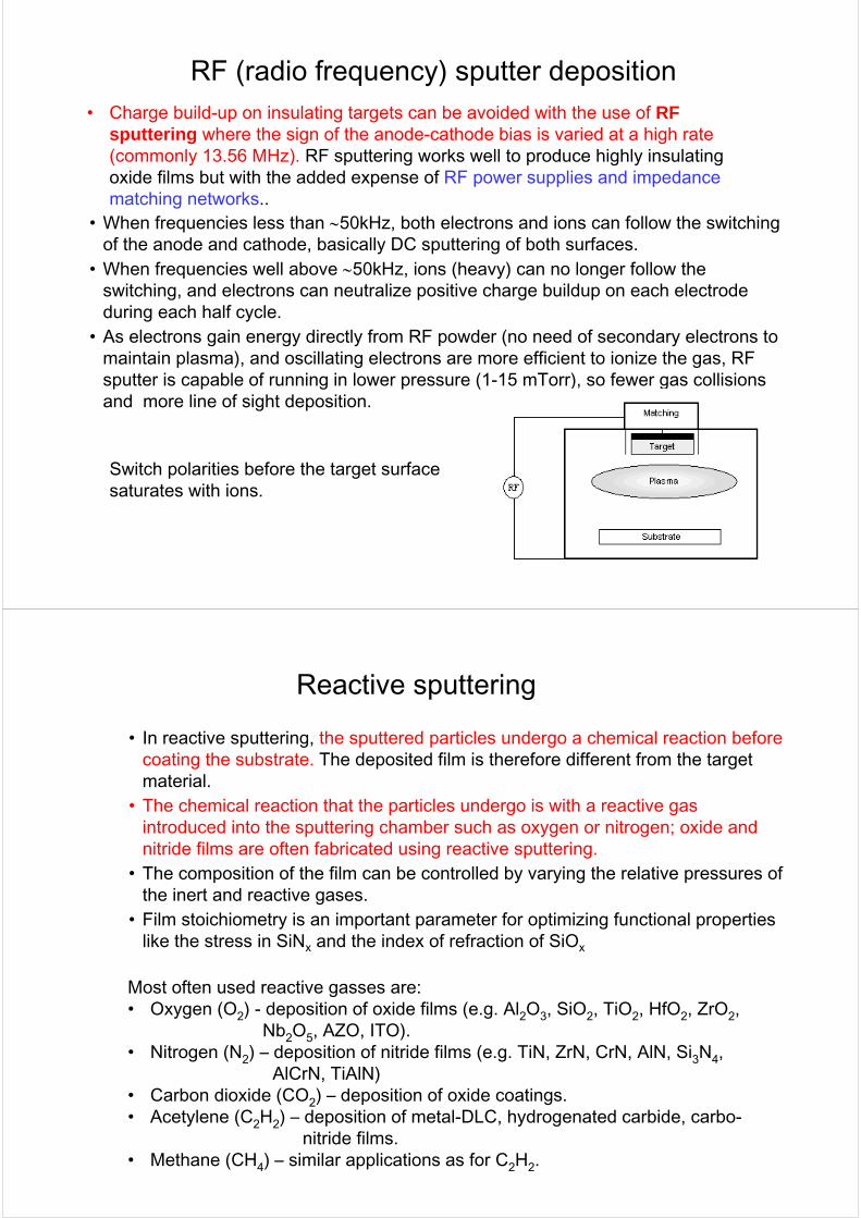
• Sputtering is a process whereby particles are ejected from a solid target material due to bombardment of the target by energetic gas ions.
• Plasma is formed by DC or RF power, and generated ions are accelerated to strike the target.
• Sputtering is driven by momentum exchange between the ions and atoms in the target materials, due to collisions.
• The incident ions set off collision cascades in the target. When such cascades recoil and reach the target surface with an energy greater than the surface binding energy, an atom would be ejected, and this process is known as sputtering.
• The sputter gas is typically an inert gas such as argon.
• Energy of each incoming ion is 500-1000eV.Energy of sputtered atoms is 3-10eV.
Electron impact ionization
DC plasma
• A small population of atoms within the cell is initially ionized through random processes. The positive ions(negative electrons) are driven towards the cathode(anode) by the electric potential.
• The initial population of ions and electrons collides with other atoms, ionizing them. As long as the potential is maintained, a population of ions and electrons remains. 19
• Plasma is an electrically neutral medium of unbound positive and negative particles. A plasma can be created by heating a gas or subjecting it to a strong electromagnetic field, applied with a laser or microwave generator.
• Electric glow discharge is a type of plasma formed by passing a current at 100 V to several kV through a gas, usually argon or another noble gas.
Magnetron sputtering
20
- Deposition rates increase by 10 ~ 100.- Unintentional wafer heating is reduced since the dense plasma is confined near the target.- A lower Ar pressure can be utilized since ionization efficiency is larger.
• Sputtering sources often employ magnetrons that utilize strong electric and magnetic fields to confine charged plasma particles close to the surface of the sputter target.
• In a magnetic field, electrons follow helical paths around magnetic field lines, undergoing more ionizing collisions with gaseous neutrals near the target surface than would otherwise occur.
• Stray magnetic fields leaking from ferromagnetic targets also disturb the sputtering process. Specially designed sputter guns with unusually strong permanent magnets must often be used in compensation.
RF (radio frequency) sputter deposition
• When frequencies less than 50kHz, both electrons and ions can follow the switching of the anode and cathode, basically DC sputtering of both surfaces.
• When frequencies well above 50kHz, ions (heavy) can no longer follow the switching, and electrons can neutralize positive charge buildup on each electrode during each half cycle.
• As electrons gain energy directly from RF powder (no need of secondary electrons to maintain plasma), and oscillating electrons are more efficient to ionize the gas, RF sputter is capable of running in lower pressure (1-15 mTorr), so fewer gas collisions and more line of sight deposition.
Switch polarities before the target surface saturates with ions.
21
• Charge build-up on insulating targets can be avoided with the use of RF sputtering where the sign of the anode-cathode bias is varied at a high rate (commonly 13.56 MHz). RF sputtering works well to produce highly insulating oxide films but with the added expense of RF power supplies and impedance matching networks..
Reactive sputtering
• In reactive sputtering, the sputtered particles undergo a chemical reaction before coating the substrate. The deposited film is therefore different from the target material.
• The chemical reaction that the particles undergo is with a reactive gas introduced into the sputtering chamber such as oxygen or nitrogen; oxide and nitride films are often fabricated using reactive sputtering.
• The composition of the film can be controlled by varying the relative pressures of the inert and reactive gases.
• Film stoichiometry is an important parameter for optimizing functional properties like the stress in SiNx and the index of refraction of SiOx
22
Most often used reactive gasses are:• Oxygen (O2) - deposition of oxide films (e.g. Al2O3, SiO2, TiO2, HfO2, ZrO2,
Nb2O5, AZO, ITO).• Nitrogen (N2) – deposition of nitride films (e.g. TiN, ZrN, CrN, AlN, Si3N4,
AlCrN, TiAlN)• Carbon dioxide (CO2) – deposition of oxide coatings.• Acetylene (C2H2) – deposition of metal-DLC, hydrogenated carbide, carbo-
nitride films.• Methane (CH4) – similar applications as for C2H2.
Dependence of deposition rate on chamber pressure
23
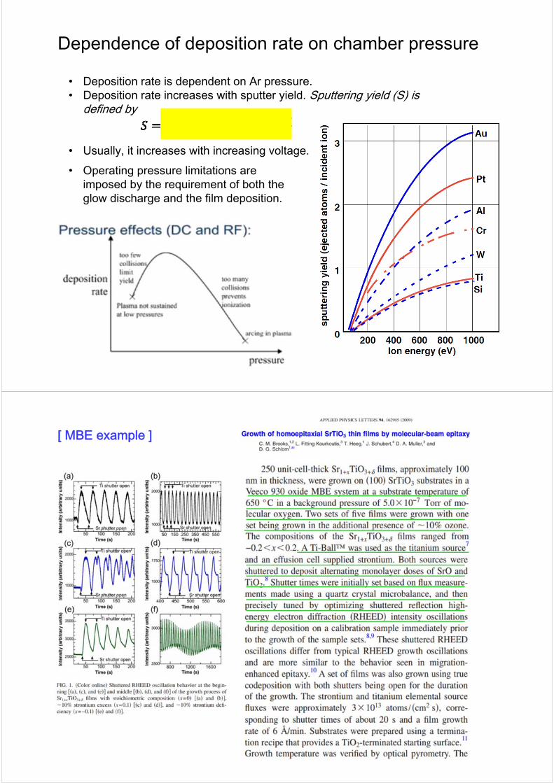
• Deposition rate is dependent on Ar pressure. • Deposition rate increases with sputter yield. Sputtering yield (S) is
defined by
• Usually, it increases with increasing voltage.• Operating pressure limitations are
imposed by the requirement of both the glow discharge and the film deposition.
[ MBE example ]
[ PLD example ]
[ Sputtering example ]
off-axis sputtering
Film properties 1. Stoichiometry: chemical composition of the film.
2. Epitaxy: the film is single crystal, and is related to the substrate
crystal orientation. Achieved by heating the substrate, so the film
atoms have energy to relax into a crystal structure commensurate
with the substrate.
3. Impurities: at high temperatures, the substrate and film atoms can
interdiffuse. Other impurity sources: target holders, walls etc.
4. Strain: the crystal spacing of film and substrate material is usually
not the same. This means the film has intrinsic strain, which can
lead to defects, film roughness, delamination.
5. Second phases: the film may phase-separate into different
regions, with different properties.
Epitaxial growth of perfect thin layers with atomic precision onto a single crystalline substrate, in order to manipulate materials properties or to design ultrathin devices.
• Atomic Layer-by-Layer Growth
High quality thin films
Single crystal substratesAtomic arrangement on the surfaceSapphire (Al2O3) crystal orientation
Slide 3-30
Polycrystalline film Oriented polycrystalline film Epitaxy film Hetero-epitaxy film
Etching & Thermal annealing• Buffered oxide etch (BOE: buffered HF or BHF) : etching thin films of SiO2 or
Si3N4. A mixture of a buffering agent, such as ammonium fluoride (NH4F), and hydrofluoric acid (HF).
(Ref.) Metal etching : A mixture of 1-5 % HNO3 (for Al oxidation), 65-75 % H3PO4 (to dissolve the Al2O3), 5-10 % CH3COOH (for wetting and buffering) and H2O dilution to define the etch rate
• Thermal annealing in gas environment for several hours using a tube furnace or a rapid thermal annealing (RTA) system is performed to make a flat and clean surface of single crystal substrate. In RTA, the wafer is heated to high temperature in seconds by a bank of heat lamps.
[example]
Surface evolution of a SrTiO3 (100) substrate through the deionized water leaching and thermal-annealing process. (a) AFM topography after 1st thermal annealing with line profile (b). (c) AFM topography after DI-water leaching with line profile (d). The final substrate is atomically flat with rms roughness of 0.2A ° . Scan area is 33 m2.
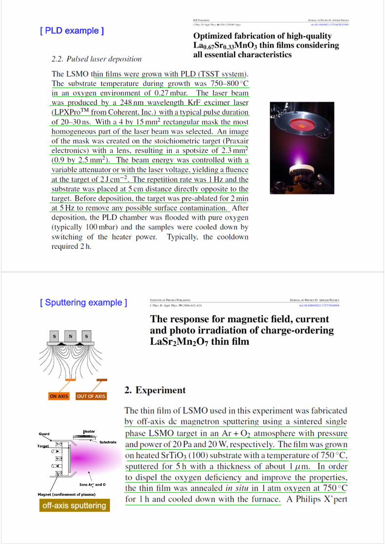
• Well-defined orientation relationship between substrate and film lattice.
Epitaxy
mathed strained relaxedAs the mismatch gets larger, the film material may strain to accommodate the lattice structure of the substrate. This is the case during the early stages of film formation (pseudomorphic growth) and with materials of the same lattice structure.
• Lattice misfit is defined as:where as,f are the lattice constants of the substrate and the film.
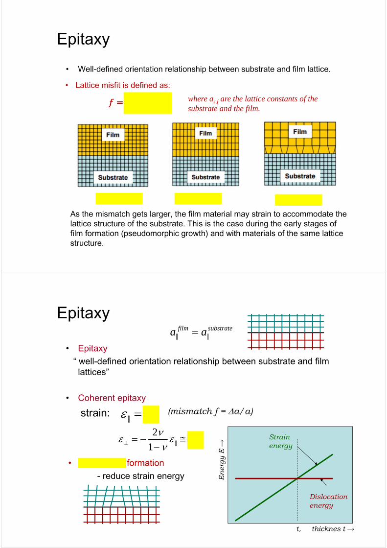
• Epitaxy“ well-defined orientation relationship between substrate and film lattices”
• Coherent epitaxy
a afilm substrate|| ||
strain: || f (mismatch f = a/a)
Epitaxy
2
1 || f
• Dislocation formation
Dislocation energy
Strain energy
tc thicknes t →
En
ergy
E →
- reduce strain energy
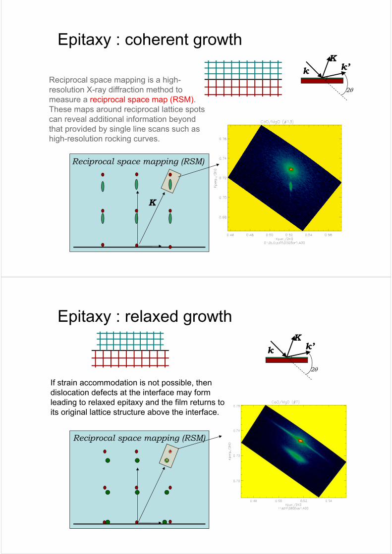
Reciprocal space mapping (RSM)
K
Epitaxy : coherent growth
k k’K
2Reciprocal space mapping is a high-resolution X-ray diffraction method to measure a reciprocal space map (RSM). These maps around reciprocal lattice spots can reveal additional information beyond that provided by single line scans such as high-resolution rocking curves.
Reciprocal space mapping (RSM)
Epitaxy : relaxed growth
k k’K
2
If strain accommodation is not possible, then dislocation defects at the interface may form leading to relaxed epitaxy and the film returns to its original lattice structure above the interface.
Morphology 1) Surface diffusion happens until nuclei of critical size are formed. 2) Capture of further ad-atoms by the nuclei forms islands.3) If diffusivity is high, the islands will merge at small sizes and yield a
smooth continuous film
Zone 1: Amorphous, low densityZone T: Specular, small grainsZone 2: Columnar grains with facetsZone 3: Larger grains, equiaxed
Structure zone diagram applicable to energetic deposition as a function of the generalized temperature T* and the normalized energy flux E* ; t* represents the net thickness.
Ref.) Materials 3, 4109(2010)
[example]
(a) AFM image (left) andRHEED image (right) of SrTiO3 (001)substrate. (b) and (c) AFM, real-timeRHEED oscillations and RHEEDimages of samples grown at 720 Cand 776 C under 1 J/cm2 laser fluence.
Laser fluence dependence of samples grown at (a) 1 J/cm2 and (b) 2.2 J/cm2, both under growth temperature of 740 C. (c) and (d) corresponding RHEED oscillations and image of the sample in (b).
Step coverage & conformality
43
poor step coverage good step coverage
non-conformal layer conformal layer
• Surfaces perpendicular to deposition source are not coated. • Step coverage describes the conformality of a thin film grown over a feature.
Non-conformal step coverage is good for liftoff, while conformal layer is good for electrical connection.
For conformal coverage, there is equal film thickness over all the topography, i.e., the vertical and horizontal surfaces have equal film thickness.
(a) Small soure, wide emitted angle distribution, but a narrow arrival angle distribution.(b) Wider arrival angle distriubtion.
Step coverageStep coverage is mainly determined by arrival angle distribution. Size of source, system geometry and collisions in gas phase are important in arrival angle distribution.
44
Standard sputtering Long-throw sputtering Sputtering with a collimator