2009 NCN@Purdue Summer School: Electronics from the Bottom Up 1 Lecture Notes on Low Bias Transport in Graphene: An Introduction Dionisis Berdebes, Tony Low, and Mark Lundstrom Network for Computational Nanotechnology Birck Nanotechnology Center Purdue University West Lafayette, Indiana USA July 13, 2009 Abstract - These notes complement a lecture with the same title presented by Mark Lundstrom and Dionisis Berdebes, at the NCN@Purdue Summer School, July 20-24, 2009. That lecture will also be available on www.nanoHUB.org in the “Electronics from the Bottom Up” section (http://nanohub.org/topics/ElectronicsFromTheBottomUp) 1. Introduction 2. Fundamentals of Graphene 3. Experimental Approach 4. Results 5. Analysis 5.1 Definition of mean-free-path for backscattering 5.2 Extraction of mean-free-path from experimental data 6. Electron Scattering in Graphene 6.1 Important scattering mechanisms in graphene 6.2 Deriving the relaxation time in graphene: an example 7. References
Transcript
2009 NCN@Purdue Summer School: Electronics from the Bottom Up
1
Lecture Notes on
Low Bias Transport in Graphene: An Introduction
Dionisis Berdebes, Tony Low, and Mark Lundstrom
Network for Computational Nanotechnology Birck Nanotechnology Center
Purdue University West Lafayette, Indiana USA
July 13, 2009
Abstract - These notes complement a lecture with the same title presented by Mark Lundstrom and Dionisis Berdebes, at the NCN@Purdue Summer School, July 20-24, 2009. That lecture will also be available on www.nanoHUB.org in the “Electronics from the Bottom Up” section (http://nanohub.org/topics/ElectronicsFromTheBottomUp)
5.1 Definition of mean-free-path for backscattering 5.2 Extraction of mean-free-path from experimental data
6. Electron Scattering in Graphene 6.1 Important scattering mechanisms in graphene 6.2 Deriving the relaxation time in graphene: an example
7. References
2009 NCN@Purdue Summer School: Electronics from the Bottom Up
2
1. Introduction In these notes, we derive some expressions that are useful in understanding low-bias transport in graphene. The notes follow the same structure as the lecture [1]. For every section, they provide proofs and calculations for the expressions that appear in the lecture. 2. Fundamentals of Graphene 2.1) Bandstructure
Figure 2.1: Graphene Bandstructure
A thorough discussion on the calculation of the dispersion relation of graphene from its Hamiltonian is available in the following nanoHUB lectures by Professor Datta (course ECE 495N – fall 2008)[13]: https://nanohub.org/resources/5710 (Lecture 21) https://nanohub.org/resources/5721 (Lecture 22)
2009 NCN@Purdue Summer School: Electronics from the Bottom Up
3
2.2) Density of States
The linearized dispersion relation, appropriate for low field transport calculations, is given by
, (2.2.1)
where is the length of the planar wave vector
, (2.2.2)
and the point represents the center of one of the six valleys of the graphene dispersion diagram. We now calculate the density of states using a summation over k space, (2.2.3)
Changing the summation into an integral, we get
, (2.2.4)
or equivalently
, (2.2.5)
where we have used (2.2.1) to justify the fact that
. (2.2.6)
We now use the Dirac function selection rule to obtain
(2.2.7)
The last step is to include a 2 for the spin and a 2 for the valley degeneracy to get that the DOS for graphene is
(2.2.8)
Calculation of DOS
2009 NCN@Purdue Summer School: Electronics from the Bottom Up
4
2.3) Number of Modes As before, the graphene dispersion relation is given by (2.3.1)
The number of modes is given as a summation over k space via the following formula
, (2.3.2)
where is the group velocity in the transport direction x
(2.3.3)
Following a similar procedure as before, we obtain
(2.3.4)
Now, considering also spin degeneracy, we get the final result for the number of conducting channels to be
(2.3.5)
Calculation of the number of modes
2009 NCN@Purdue Summer School: Electronics from the Bottom Up
5
2.4) Formula for Transmission For a derivation of the expression for the transmission function in the Landauer – Büttiker formalism, we refer the reader to Datta, Section 2.2, [14]. 2.5) Carrier Density The net carrier density n-p, where n stands for the filled states for , and p for the empty states with , is calculated as the convolution of the density of states with the Fermi Dirac distribution in the energy space. As already proven before, the density of states per unit energy and volume is given by,
(2.5.1)
Now, we can proceed to the calculation of carrier density for the general, nonzero case
(2.5.2)
The energy space over which the integration is done includes also negative energies, accounting for the valence band of graphene. Generally, one has to be careful with the Fermi Integral notation,
(2.5.3)
where
(2.5.4)
and the Gamma function of order . For a detailed discussion of Fermi-Dirac integrals, we refer the reader to the notes available on nanohub by Raseong Kim and Mark Lundstrom[15]: https://nanohub.org/resources/5475
Calculation of Carrier Density
2009 NCN@Purdue Summer School: Electronics from the Bottom Up
6
The zero temperature approximation is now easy to extract from relation (2.5.2) by making the following substitution,
, (2.5.3)
which will lead to the following
(2.5.4)
or equivalently
(2.5.5)
Finally, we get that
, (2.5.6)
which is a simple expression that relates the Fermi energy to the carrier concentration. If we want to account for the sign of the charge of the carrier that is transported in the system, we can rewrite (2.5.5) as
(2.5.7)
2.6) Conductance
In the calculation, we consider two distinct limits:
• Ballistic limit:
• Diffusive limit:
2.6a) Ballistic limit The number of conducting channels is
. (2.6.1)
The transmission function is
Calculation of Conductance
M(E)
T(E)
2009 NCN@Purdue Summer School: Electronics from the Bottom Up
7
. (2.6.2)
We begin the calculation of conductance from the Landauer formula,
(2.6.3)
where is equal to
(2.6.4)
Introducing (2.6.1), (2.6.2) and (2.6.4) into (2.6.3), we have equivalently
(2.6.5)
Now, noticing that the composite exponential expressions of (2.6.5) can be written as derivatives of Fermi functions with opposite signs for , we can use integration by parts, to obtain
(2.6.6)
Now we can yield our final result
, (2.6.7)
In the zero temperature approximation, , thus the expression (2.6.3) for
conductance, in the ballistic limit, can be reduced to
, (2.6.8)
2009 NCN@Purdue Summer School: Electronics from the Bottom Up
8
according to the Dirac function selection rule. 2.6b) Diffusive Limit The transmission function is
, (2.6.9)
where we assume a mean free path of the form, .
Again, we begin our calculation for conductance from
. (2.6.10)
Now, introducing (2.6.9) and (2.3.5) into (2.6.10) we have
(2.6.11)
We again proceed to the formation of the proper derivatives, in a similar manner to our previous treatment for the ballistic case,
(2.6.12)
In this general treatment, the integration by parts will not absorb the energy monomial term, but still things don’t get too complicated,
2009 NCN@Purdue Summer School: Electronics from the Bottom Up
9
(2.6.13)
In the zero temperature approximation, the diffusive expression for conductance can be reduced to
(2.6.14)
Note: There are restrictions that apply on the value of . A negative value of the characteristic exponent will not yield a meaningful calculation, since the diffusive limit assumption will no longer hold for the energy range integrated in the vicinity of zero (mean free path driven to infinity). Thus, one should consider only for a meaningful analytical expression.
2009 NCN@Purdue Summer School: Electronics from the Bottom Up
10
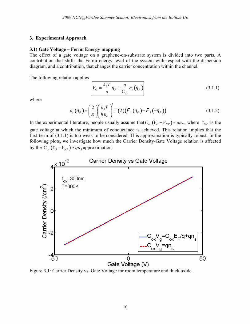
3. Experimental Approach 3.1) Gate Voltage – Fermi Energy mapping The effect of a gate voltage on a graphene-on-substrate system is divided into two parts. A contribution that shifts the Fermi energy level of the system with respect with the dispersion diagram, and a contribution, that changes the carrier concentration within the channel. The following relation applies
(3.1.1)
where
(3.1.2)
In the experimental literature, people usually assume that , where is the gate voltage at which the minimum of conductance is achieved. This relation implies that the first term of (3.1.1) is too weak to be considered. This approximation is typically robust. In the following plots, we investigate how much the Carrier Density-Gate Voltage relation is affected by the approximation.
Figure 3.1: Carrier Density vs. Gate Voltage for room temperature and thick oxide.
2009 NCN@Purdue Summer School: Electronics from the Bottom Up
11
Figure 3.2: Carrier Density vs. Gate Voltage for zero temperature and thick oxide
Figure 3.3: Carrier Density vs. Gate Voltage for room temperature and thin oxide
2009 NCN@Purdue Summer School: Electronics from the Bottom Up
12
Figure 3.4: Carrier Density vs. Gate Voltage for zero temperature and thin oxide It is interesting to note, that the assumption generally made in the experimental literature, performs well. It remains valid over a large range of temperatures, but it breaks down for very small oxide thicknesses. For 90 nm or 300 nm, which are the typical thicknesses, however, one can assume that with confidence. 3.2) Quantum Capacitance Central to the discussion in section 3.1 is the concept of quantum capacitance. The quantum capacitance of a carrier density is calculated as the derivative of carrier density vs. energy at the Fermi energy, (3.2.1)
In addition, the electron concentration is related to the Fermi energy as follows
(3.2.2)
Thus
Calculation of Quantum Capacitance
2009 NCN@Purdue Summer School: Electronics from the Bottom Up
13
(3.2.3)
Now, the quantum capacitance can be extracted
(3.2.4)
4. Results 4.1) Sheet Conductance for The general expression for conductance for a single principal scattering mechanism, at the diffusive limit, has been derived to be (2.6.14)
(4.1.1)
We can write the conductance as
(4.1.2)
From (4.1.1) and (4.1.2), one can yield the sheet conductance vs to be
, (4.1.3)
It is interesting to focus on what the Landauer theory predicts for the minimum sheet conductance. In particular, if we substitute , we get
(4.1.4)
where is the characteristic exponent of the principal scattering mechanism as defined in (2.6.9). Please note that we can recover the ballistic conductivity at the minimum by substituting
and .
2009 NCN@Purdue Summer School: Electronics from the Bottom Up
14
4.2) Calculation details of slides 24-27 The temperature of the system is . It is possible to assume the zero-T approximation for both the ns/Vg/Ef relation and for the expression for conductance. In addition, the linear behavior of conductivity vs gate voltage suggests strong presence of scattering with mean free path with characteristic exponent s=1. Thus, we can write down:
(4.2.1)
(4.2.2)
(4.2.3)
(4.2.4)
From (4.2.1-3), one can derive the Fermi energy from a given gate voltage value ( ). Then, taking the values for conductivity at these voltages and using (4.2.4) one can calculate . Please note that for this particular sample, the linearity of sheet conductance vs. carrier concentration/gate voltage should suggest a mobility that is independent of carrier density. 5. Analysis 5.1 Definition of mean-free-path for backscattering - Landauer Approach vs. the Boltzmann Transport Equation Approach For diffusive transport, the conductance is frequently computed by solving the Boltzmann transport equation, so the question arises as to how the two approaches compare with each other. From the Landauer approach for graphene in the diffusive limit at T = 0K, we have
(5.1.1)
or
(5.1.2)
How does this compare to the result obtained by solving the BTE? Begin with the steady-state BTE without density gradient (Lundstrom, 3.2 [2])
2009 NCN@Purdue Summer School: Electronics from the Bottom Up
15
(5.1.3)
Assuming the Relaxation Time Approximation (RTA) for the collision integral (Lundstrom, 3.3.2 [2]), this equation becomes
(5.1.4)
which is valid for isotropic or elastic scattering with then being the momentum relxation time [2]. Assuming a voltage drop of V across a resistor of length L, we use the chain rule for the derivative
(5.1.5)
which can be solved to find
(5.1.6)
The current per unit width is evaluated from
(5.1.7)
Converting the sum to an integral,
(5.1.8)
The first factor of 2 is for spin and the second is for valley degeneracy. Using , we find
(5.1.9)
The integral over k can be converted to an integral over energy using the dispersion (i.e. ) for graphene
(5.1.10)
to find
(5.1.11)
from which we find
(5.1.12)
2009 NCN@Purdue Summer School: Electronics from the Bottom Up
16
at T = 0K,
(5.1.13)
so the integral becomes
(5.1.14)
which can be written as
(5.1.15)
which is exactly eqn. (5.1.2) from the Landauer approach provided we define the “mean-free-path” for backscattering to be
(5.1.16)
Finally, note that the BTE result (5.1.14) is often written in another way. Recall that the density of states for graphene is
(5.1.17)
so eqn. (5.1.14) can be written as
(5.1.18)
or recognizing the diffusion coefficient for electrons at energy, E, as
(5.1.19)
we can write the sheet conductance from the BTE as (5.1.20)
which is true in general, not just for graphene.
2009 NCN@Purdue Summer School: Electronics from the Bottom Up
17
5.2 Extraction of the apparent mean-free-path from experimental data
Figure 5.1: Inputs and outputs of experimental data analysis As it can be seen in the schematic, in the analysis of experimental data, we need the dimensions of the system, the temperature of the environment, the applied voltages and the measured conductance. In the extraction of the mean free path, we assume a zero temperature approximation. In this case, we have
, (5.2.1)
or for the sheet conductance
. (5.2.2)
We now define an apparent mean free path
, (5.2.3)
which is equivalent to writing
(5.2.4)
The relation between sheet conductance and conductance was discussed also in section 4.1. In this section, however, the difference between the mean free path and the apparent mean free path is clarified. This need didn’t arise in 4.1, because at the diffusive limit, . Now, one can extract a zero temperature approximation apparent mean free path that depends on Fermi energy as follows
METHOD
2009 NCN@Purdue Summer School: Electronics from the Bottom Up
18
(5.2.5)
Usually, one has experimental input of the form , thus one might also use (4.2.1) to get
(5.2.6)
Now, we can recover the mean free path to be compared with scattering theory with the use of (5.2.4), if we know the length of the sample. 6. Electron Scattering in Graphene The measured conductance of graphene depends on the microscopic scattering processes that occur. This is still an active field of research. In these notes, we only wish to review some of the major features of scattering in graphene and to discuss briefly how scattering rates are computed. 6.1 Important scattering mechanisms in graphene Identifying the major scattering mechanisms limiting the transport properties of graphene is important from a device point of view. In this section, we shall review some of the commonly known scattering mechanisms believed to be playing an important role in graphene. Short range scattering potential due to localized defects has been discussed in the literature [3,11,12], where one usually approximate the scattering potential by a delta function. The important point is that short range scattering potentials give rise to a scattering time (and mean-free-path) that varies as and is independent of temperature. Charged impurity scattering is thought to be an important scattering mechanism in graphene [7]. For unscreened Coulomb scattering, one finds [3,8] that , which leads to a conductance that is proportional to . In practice, we expect the charges to be screened by the carriers in the graphene. In fact, the observation of a linear conductance vs. characteristic is frequently taken as evidence for the presence of charged impurity scattering. It has been pointed out, however, that uncharged defects can also lead to this behavior, if the scattering potential is strong enough to induce mid-gap states [9]. Recent experimental studies on intentionally damaged graphene have shown that strong defect scattering can produce linear conductance vs. . Deformation potential scattering by acoustic phonons [4,9] is also believed to be an important scattering mechanism. The precise value of is is uncertain with values from 10-30 eV being reported [4]. Optical phonons in the graphene can also scatter carriers – especially at temperatures above 300K [5]. Some authors believe that optical phonon in graphene are responsible for the decrease in conductivity at high temperatures [5] while others feel that polar optical phonon in the underlying SiO2 are responsible [6].
2009 NCN@Purdue Summer School: Electronics from the Bottom Up
19
6.2 Deriving relaxation time in graphene: an example In this section, we illustrate how to derive the momentum relaxation time in graphene. We shall consider the deformation potential (ADP) scattering as an example. The main physics follow the classic approach described in [2], pp. 64-67, 73-82). The only modification that one made to this simple approach [2] is to account for the fact that the graphene wavefunction is described by a two-component wavefunction as follows:
(6.2.1)
where
(6.2.2)
This arises from the property of the linear dispersion relationship of graphene. The overlap between two plane waves is
(6.2.3)
This then yields us the overlap probability
(6.2.4)
We first identify the perturbing potential as ([2], p. 60- 61) (6.2.5) Writing the Fourier components of the acoustic wave as (6.2.6) and inserting the result in eqn. (15), we find (6.2.7) We wish to described the transition rate (probability per second) for scattering from the incident state, , to the final state, . This is usually done using first order perturbation theory (Fermi’s Golden Rule) as ([2], pp. 41-46)
(6.2.8)
where the matrix element is (6.2.9)
2009 NCN@Purdue Summer School: Electronics from the Bottom Up
20
The energy of the scattered electron is (6.2.10) where is the change in energy as a result of scattering (zero for elastic scattering). Static potentials cause elastic scattering, and time-varying potentials describe inelastic scattering. For acoustic phonons, the scattering potential is simply a constant with respect to the integration variables in (6.2.9). So we can write Eq. (6.2.8) as
(6.2.11)
where, following the arguments in [2] (pp.73-74), we have assumed that acoustic phonon scattering near room temperature is elastic. In this expression, the Kronecker delta expresses momentum conservation, and the delta function, energy conservation. Next, we must quantize the lattice vibrations by replacing the magnitude of the classical wave in (6.2.6) by its quantum mechanical counterpart (see [2], pp. 77-78)
(6.2.12)
Where the top sign denotes acoustic phonon emission and the bottom sign, absorption. The number of acoustic phonons is give by the Bose-Einstein occupation factor
(6.2.13)
For a typical acoustic phonon involved in electron-phonon scattering, ([2], pp. 73-74), so we can expand the exponential in (6.2.13) and find .
(6.2.14)
As a result of 6.2.14, we find
(6.2.15)
So we can just sum the absorption and emission rates. Returning to (6.2.12), M is the total mass within the normalization area, A, (6.2.16) For small wave-vector, β, the acoustic phonon dispersion is linear ([2], pp. 46-48), so
2009 NCN@Purdue Summer School: Electronics from the Bottom Up
21
(6.2.17)
Since these are the low energy phonons involved in elastic ADP scattering, we can use 6.2.17 along with eqns. (6.2.11-15) in the expression for the transition rate, (6.2.80) to find
(6.2.18)
From the transition rate, we find the total scattering rate as
(6.2.19)
We arrive at the same result as [4,9]. According to [4], the acoustic deformation potential for graphene is eV, the velocity of LA phonons is cm/s, and the mass density is kg m-2.
2009 NCN@Purdue Summer School: Electronics from the Bottom Up
22
References [1] Mark Lundstrom and Dionisis Berdebes, “Low Bias Transport in Graphene: An
Introduction,” lecture presented at the NCN@Purdue Summer School on Electronics from the Bottom Up, Purdue University, July 20-24, 2009 (to appear on www.nanoHUB.org).
[2] Mark Lundstrom, Fundamentals of Carrier Transport, 2nd Ed., Cambridge University
Press, 2000. [3] N.M.R. Peres, J.M.B. Lopes dos Santos, and T. Stauber, “Phenomenological study of the
electronic transport coefficiencts in graphene, Phys. Rev. B, 76, 073412, 2007. [4] E.H. Hwang and S. Das Sarma, “Acoustic phonon scatterig limited carrier mobility in
two-dimensional extrinsic graphene,” Phys. Rev. B, 77, 115449, 2008. [5] R.S. Shishir and D.K. Ferry, “Intrinsic mobility in graphene,” J. of Phys.: Condensed
Matter, 21, 232204, 2009. [6] J.-H Chen, C. Jang, S. Xiao, M. Ishigami, and M.S. Fuhrer, “Intrinsic and extrinsic
performance limits of graphene devices on SiO2,” Nature Nanotechnology, 3, pp. 206-209, 2008.
[7] J.-H. Chen, C. Jang, S. Adam, M.S. Fuhrer, E. D. Williams, and M. Ishigami, “Charged-
impurity scattering in graphene,” Nature Phys., 4, 377, May, 2008. [8] S. Adam, E. H. Hwang, V. M. Galitski and S. Das Sarma, “A self-consistent theory for
graphene transport,” Proc. Nat. Aca. Sci. 104, 18392, 2007 [9] T. Stauber, N.M.R. Peres, and F. Guinea, “Electronic transport in graphene: A
Semiclassical approach including midgap states,” Phys. Rev. B, 76, 205423, 2007. [10] B.R. Nag, Electron Transport in Compound Semiconductors, Springer-Verlag, New
York, 1980. [11] T. Ando and T. Nakanishi, “Impurity scattering in carbon nanotubes: Absence of back
scattering,” J. Phys. Soc. Jap. 67, 1704, 1998 [12] N. H. Shon and T. Ando, “Quantum transport in two-dimensional graphite system”, J.