Novel Substrate Integrated Waveguide Filters and Circuits Liwen Huang Submitted in accordance with the requirements for the degree of Doctor of Philosophy The University of Leeds School of Electrical and Electronic Engineering July 2013
Transcript
Novel Substrate Integrated Waveguide Filters and Circuits
Liwen Huang
Submitted in accordance with the requirements for the degree of
Doctor of Philosophy
The University of Leeds
School of Electrical and Electronic Engineering
July 2013
The candidate confirms that the work submitted is her own and that
appropriate credit has been given where reference has been made to the
work of others.
The candidate confirms that the work submitted is her own, except where
work which has formed part of jointly-authored publications has been
included. The contribution of the candidate and the other authors to this work
has been explicitly indicated below. The candidate confirms that appropriate
credit has been given within the thesis where reference has been made to
the work of others.
This copy has been supplied on the understanding that it is copyright
material and that no quotation from the thesis may be published without
superconductor filters [63, 64], and a variety of coaxial, finline and microstrip
filters [1-4].
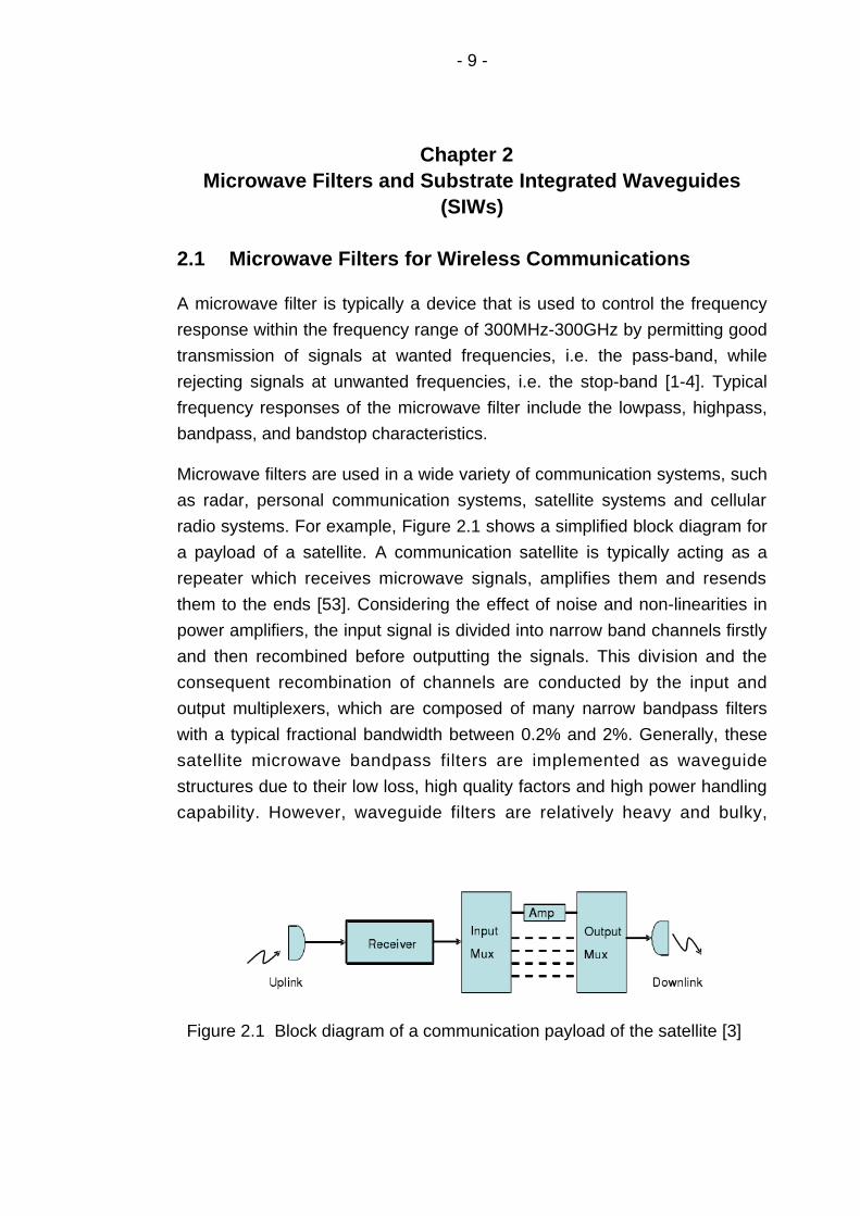
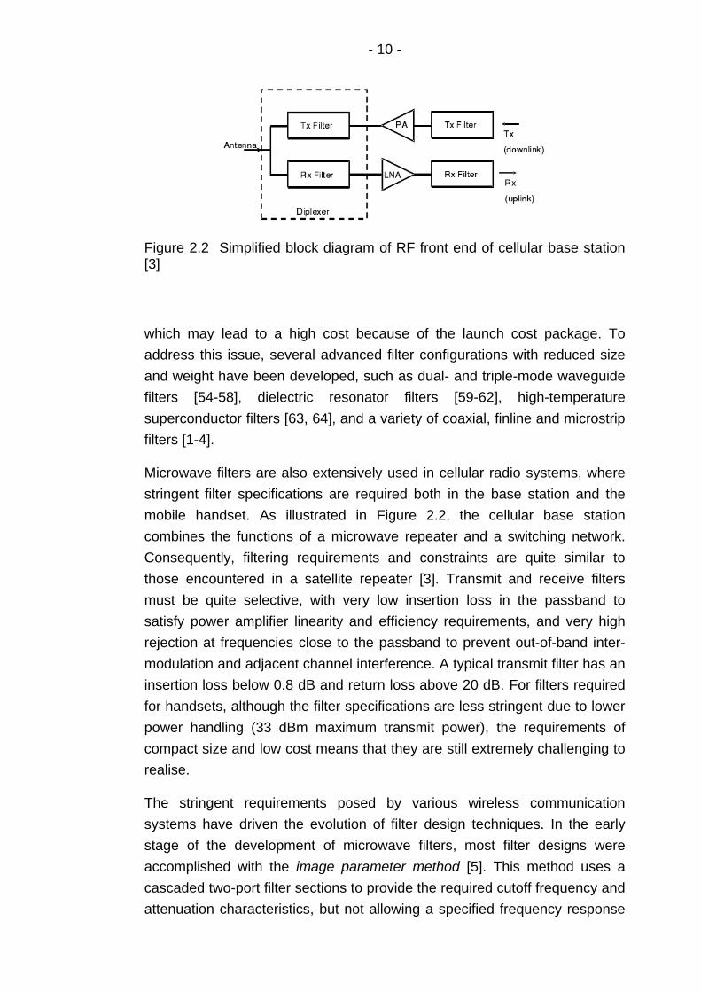
Microwave filters are also extensively used in cellular radio systems, where
stringent filter specifications are required both in the base station and the
mobile handset. As illustrated in Figure 2.2, the cellular base station
combines the functions of a microwave repeater and a switching network.
Consequently, filtering requirements and constraints are quite similar to
those encountered in a satellite repeater [3]. Transmit and receive filters
must be quite selective, with very low insertion loss in the passband to
satisfy power amplifier linearity and efficiency requirements, and very high
rejection at frequencies close to the passband to prevent out-of-band inter-
modulation and adjacent channel interference. A typical transmit filter has an
insertion loss below 0.8 dB and return loss above 20 dB. For filters required
for handsets, although the filter specifications are less stringent due to lower
power handling (33 dBm maximum transmit power), the requirements of
compact size and low cost means that they are still extremely challenging to
realise.
The stringent requirements posed by various wireless communication
systems have driven the evolution of filter design techniques. In the early
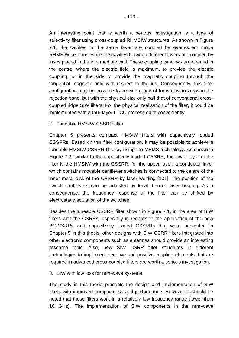
stage of the development of microwave filters, most filter designs were
accomplished with the image parameter method [5]. This method uses a
cascaded two-port filter sections to provide the required cutoff frequency and
attenuation characteristics, but not allowing a specified frequency response
- 11 -
over the complete operating range. Therefore, even though the design
procedure is relatively simple, such designs require many iterations and
empirical adjustments to achieve the desired results and there is no
methodical way to improve the design. Later, with the development of
network synthesis techniques, a new method, termed the insertion loss
method, was developed to provide a systematic way for synthesizing the
required filtering performance [5]. Filter design procedures with the insertion
loss method begin with a low-pass filter prototype that is normalized in terms
of impedance and frequency. The prototype is then converted to the desired
filter by using the frequency and impedance transformations. Compared to
the image parameter method, the insertion loss method allows the design of
filters with a completely specified frequency response and it has a higher
degree of control over the passband and stopband characteristics. Today,
with the advances in computer-aided design (CAD) technologies, synthesis
techniques coupled with accurate electromagnetic simulations as well as
sophisticated optimization software algorithms have allowed the design of
filters to go from drawing boards almost immediately to the final product,
without the need for empirical adjustments or manual tuning. This not only
cuts dramatically the time required for product development cycle, but also
provides more opportunity for the implementation of more efficient
communication systems.
In the meantime, significant efforts have also been devoted to the research
and development of advanced microwave structures for the implementation
of microwave filters. There are mainly three categories of structures
commonly used in the physical realisation of filters: the lumped-element LC
structure, the planar microwave structure, and the three-dimensional cavity
structure [4]. Lumped-element LC structures [1] are typically composed of
chip inductors and capacitors. This type of structures is generally employed
in the implementation of filters operating at low frequencies, with a small size
but relatively low Q-factor. Microstrip and stripline filters [2] are constructed
out of sections of transmission lines terminated in a short or open circuit with
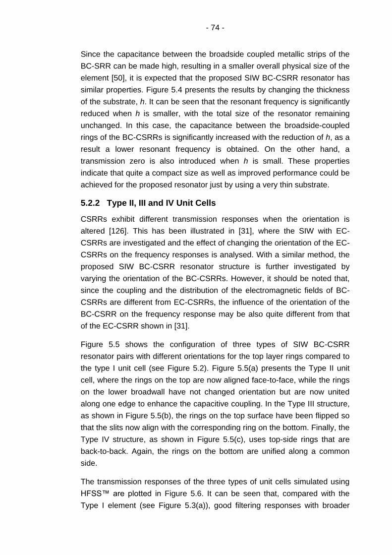
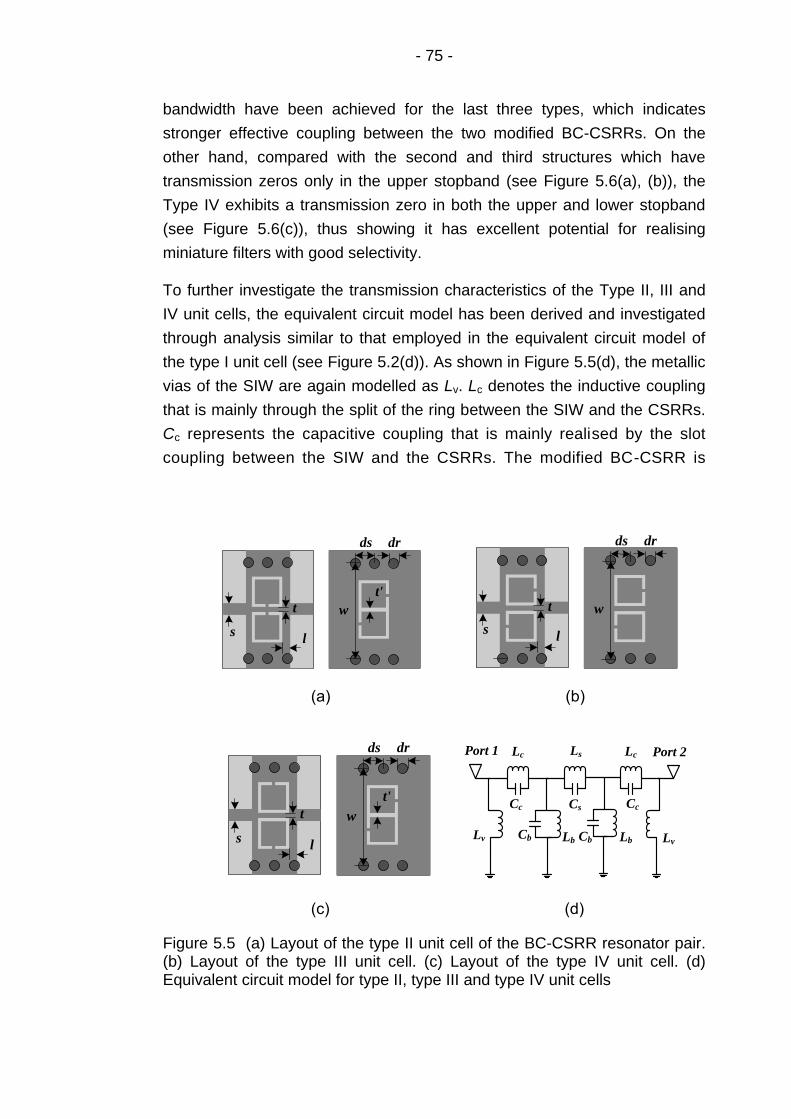
various shapes, for example, hairpin [65], ring [66] and patched [67]
configuration. These planar microwave filters have the advantages of
compact sizes, low cost, easy fabrication and integration with other circuits,
but they are relatively lossy (Q factors between 50 and 300 at 1 GHz [4]) and
have limited power capability. In contrast, cavity filters such as dielectric [68],
waveguide and coaxial [69, 70] filters have quite high Q-factors (up to 30000
[4]) and high power handling levels. However, they are relatively bulky and
- 12 -
difficult to fabricate and integrate with other circuits in comparison to their
counterparts implemented with planar structures.
Recently, with the advent of a new structure termed the “substrate integrated
waveguide” (SIW) [6], it has become possible to combine the main
advantages of the waveguide cavity with that of the low cost and high
integrated planar circuits. The SIW is a waveguide-like structure which can
be fabricated on a planar dielectric substrate by using periodic metallic via
holes as side walls. It preserves both the benefits of waveguide cavity
structures and printed planar circuits such as low loss, high Q-factor, high
power handling capability, compact sizes as well as easy fabrication and
integration [6, 71-74]. Hence, the SIW provides a promising platform for the
development of microwave filters with high performance and miniaturized
size. Furthermore, it also offers a promising platform to develop cost-
effective, easy-to-fabricate and high-performance communication systems
by integrating filters with other electronic circuits on the same substrate,
such as planar circuitry, active components and antennas.
Today, the great advances in novel materials and technologies have further
driven the rapid development of filters. Several new materials and structures,
such as high-temperature superconductors (HTS) [75], low-temperature
cofired ceramic (LTCC) [76-78], photonic bandgap (PBG) [79, 80] and
electromagnetic bandgap (EBG) structures [81-84] have been applied in the
design of filters to improve the performance and reduce the size. Several
advanced techniques such as monolithic microwave integrated circuits
(MMIC) [85, 86] and microelectromechanical systems (MEMS) [87-89] have
provided more flexibility for the physical realisation of microwave filters. In
the meantime, advances in network synthesis techniques and computer-
aided design tools have enabled the accurate design and simulation of some
advanced filters, namely, the cascaded quadruplet (CQ) filters [90, 91],
cascaded trisection (CT) filters [92, 93] and cross-coupled filters [94-97].
With the continuing advances in fabrication techniques as well as synthesis
techniques and computer-aided design techniques, it is expected that the
investigation of advanced filters with higher performance, lower cost and
smaller size continue to be an important research topic.
- 13 -
2.2 Design of Microwave Filters
2.2.1 Approximation of the Transfer Function
The design of a microwave filter usually starts with the determination of a
transfer function which approximates the required filter specification. An
ideal filter has a zero attenuation in the passband and infinite attenuation in
the stopband. Such an ideal transfer function cannot be realised in practice.
However, it can be approximated with a filtering function in the domain of the
equivalent circuit [1-4]. Generally, there are various functions that can be
used for approximation. Here, we will focus on several classic functions,
including the Butterworth (maximally flat), Chebyshev and elliptic functions.
2.2.1.1 General Definition
The transfer function for a two-port lossless passive filter network is defined
as [2] :
2
21 2 2
1
1 n
S jF
(2-1)
where ε represents a ripple constant; ω is a frequency variable; Fn(ω) stands
for a filtering or characteristic function. For a given transfer function of (2-1),
the insertion loss response of the filter can be written as follows:
10 2
21
110AL log dB
S j
(2-2)
For a lossless, passive two-port network, since 2 2
11 21 1S S , the return
loss of the filter can then be computed by:
2
10 2110 1RL log S j dB
(2-3)
2.2.1.2 Butterworth Function Approximation
The Butterworth approximation provides the simplest approximation to an
ideal prototype filter [3]. The Butterworth approximation is defined by:
nK (2-4)
where n is the order of the prototype filter, which corresponds to the number
of reactive elements required in the lowpass prototype filter. The S-
parameters of the filter prototype can be expressed as:
- 14 -
2
21 2
1
1 nS j
(2-5)
2
2
11 21
n
nS j
(2-6)
Hence, the insertion loss is given by:
2
1010 1 n
AL log (2-7)
The Butterworth approximation demonstrates maximal possible flatness of
the insertion loss curve. The 3-dB cutoff frequency occurs at ωc = 1 rad/sec
and marks the transition between the passband and stopband. This
transition becomes more rapid when the order of the filter is higher. Typical
Butterworth prototype responses with various filter order are presented in
Figure 2.3.
2.2.1.3 Chebyshev Function Approximation
The Butterworth approximation provides flat response in the passband but it
rolls off quite slowly especially for low-order filters. A better approximation
can be achieved if ripples exist in the passband but with more rapid roll off in
the stopband. A Chebyshev approximation is defined as [3]:
nK T (2-8)
where ε is the ripple constant that is related to the maximum in-band ripple
LAr in dB by 101 10 1ArL /
/ ; Tn(ω) is a Chebyshev function of the first
kind of order n, which can be expressed by Tn(ω)=cos(n*cos-1ω).
Figure 2.3 Butterworth response for various filter order, n
- 15 -
The expressions for S-parameters of the filter prototype are given by:
2
21 2 2
1
1 n
ST
(2-9)
22
11 2 21
n
n
TS
T
(2-10)
The insertion loss can thus be expressed as:
2 2
1010 1A nL log T (2-11)
The Chebyshev approximation is capable of providing sharper slope for a
lower filter order (n) compared to the Butterworth approximation, but with
equal ripples introduced in the passband. A typical frequency response of
the Chebyshev prototype filter is illustrated in Figure 2.4.
2.2.1.4 Elliptic Function Approximation
The Butterworth and Chebyshev approximation are referred to as all-pole
approximations as all the transmission zeros are located at infinity [3].
However, placing transmission zeros at finite frequencies are quite important
in some applications where a rapid roll off is required. An elliptic function
approximation is equiripple in both the passband and the stopband. The
elliptic function approximation is capable of producing transmission zeros at
finite frequencies and thus exhibits the optimum response in terms of
selectivity. Nevertheless, it should be noted that the transmission zeros of
the elliptical approximation is prescribed by filter specifications, and hence
these transmission zeros are restricted to be at certain frequencies and
there is no flexibility in their locations.
Figure 2.4 Chebyshev response
- 16 -
Figure 2.5 Elliptic function response
For a specific prototype with m transmission zeros ωz1 …ωzm, and k poles
ωp1 …ωpk, the transfer function can be expressed in the following form:
2
21 2 2 2 2
1
2 2 2 2
1
1
1P Pk
Z Zm
S
(2-12)
The attenuation is thus given by:
2 2 2 2
1
10 2 2 2 2
1
10 1P Pk
A
Z Zm
L log
(2-13)
A typical frequency response of the prototype filter with elliptic function is
shown in Figure 2.5.
2.2.2 Lowpass Prototype Networks
The next step of the filter design is the synthesis of the equivalent circuit to
reproducing the transfer function characteristics that are derived from the
approximation process. This equivalent circuit should model the electrical
performance of the real construction that is used for implementation of filters,
and acts as an interface between the abstract filtering function and the
practical filter structure, so that the physical dimensions of filters could be
obtained from the element values of the prototypes. Generally, a normalized
lowpass filter prototype is chosen as an equivalent network, with the values
of the source resistance or conductance equal to one (denoted by g0 = 1)
and the cutoff angular frequency to be unity (denoted by Ωc = 1 rad/s). This
lowpass filter prototype can be further converted to the desired highpass,
bandpass and bandstop filter prototypes by using frequency and element
transformations (see the following section 2.2.3) [1, 2].
- 17 -
One of the most commonly used circuits for realisation of rational functions
in filter design is the ladder network [1, 2]. The ladder network is composed
of alternating series and parallel impedances in ladder configuration. Figure
2.6 presents two typical forms of the ladder network for realising an all-pole
filter response. These two forms are dual from each other and hence either
form can serve as a prototype for the design of filters with an all-pole
response, such as the Butterworth and Chebyshev responses.
2.2.2.1 Butterworth Lowpass Prototype
For the Butterworth lowpass filter prototypes with an insertion loss LAr = 3 dB
at the cutoff frequency Ωc = 1, the element values for the two-port networks
shown in Figure 2.6 can be computed by [2, 3]:
0
1
1 0
2 12 1 2
2
1 0
i
n
g .
ig sin i , , ,n
n
g .
, (2-14)
As can be seen from (2-14), the Butterworth filter prototype considered here
has a symmetrical network structure, namely, g0 = gn+1, g1 = gn and so on.
(a)
(b)
Figure 2.6 Lowpass prototype filters for all-pole filters with: (a) a ladder network structure, and (b) its dual [2]
- 18 -
For a given filter specification with the minimum return loss LAr at the
frequency Ω = Ωp, and the minimum insertion loss LAS at Ω = Ωs, the order of
the Butterworth lowpass prototype, which will satisfy this specification, can
be determined with the following formula [2, 3]:
0 1
10
10 10
10 1
2 20
AS. L
Ar AS
s s p
log L Ln max ,
log log /
(2-15)
2.2.2.2 Chebyshev Lowpass Prototype
For a Chebyshev lowpass prototype filter with a passband ripple LAr and the
cutoff frequency Ωc = 1, the element values shown in Figure 2.6 can be
computed by [2, 3]:
0
1
1 2 2
1 2
1 0
2
2
2 1 2 34
2 212 3 4
1
1 0
4
i
i
n
g .
g sinn
i isin sin
n ng i , , .n
g isin
n
. for n odd
gcoth for n even
,
(2-16)
where 17 37
ArLln coth
.
,
2sinh
n
. Some typical element values for
such filters can be found in literature such as [1-3].
The degree of the Chebyshev prototype, with the required passband ripple
LAr and the minimum stopband attenuation LAS dB at Ω = Ωs, is given by [2]:
0 11
0 1
1
10 1
10 1
AS
Ar
. L
. L
s
cosh
ncosh
(2-17)
2.2.2.3 Elliptic Function Lowpass Prototype
The elliptic function lowpass filter prototype has finite real frequency
transmission zeros and hence this prototype cannot be realised with
conventional ladder networks shown in Figure 2.6. Figure 2.7 presents two
- 19 -
modified ladder network structures for realisation of elliptic function lowpass
prototype filters, where series and parallel resonant circuits are introduced to
obtain the transmission zeros. As shown in Figure 2.7(a), series branches of
parallel-resonant circuits are used to implement the finite-frequency
transmission zeros, as they block the transmission of signals by having
infinite series impedance (open-circuit) at resonance. For the dual form
illustrated in Figure 2.7(b), the shunt branches of series-resonant circuits are
employed to realise transmission zeros, as they are capable of shorting out
signal transmission at resonance [2]. Besides the ladder network, an
alternative technique of obtaining transmission zeros at finite frequencies is
using the cross-coupled network topologies [2]. More details on synthesis of
the elliptic function lowpass filter prototype with the ladder network and the
cross-coupled network can be found in literatures such as [2, 3].
2.2.3 Frequency and Element Transformations
The lowpass prototype filters discussed above has a cutoff frequency Ωc = 1
and a normalized source impedance g0 = 1. These restrictions make them
unsuitable for practical use. Therefore, it is necessary to apply the frequency
and element transformations in order to obtain the frequency responses and
element values for practical filters. The frequency transformation, also
(a)
(b)
Figure 2.7 Lowpass prototype filters for elliptic function filters with: (a) series parallel-resonant branches, and (b) its dual with shunt series-resonant branches [2]
- 20 -
known as frequency mapping, is capable of mapping a response in the
lowpass prototype frequency domain Ω into the real angular frequency
domain ω, where a practical filter response is expressed (such as lowpass,
highpass, bandpass and bandstop). It has an effect on all the reactive
elements, but with no effect on the resistive elements. For the impedance
transformation, it can remove the normalization of the source impedance in
the lowpass prototypes (g0 = 1) and adjust the filter to work for any value of
the source impedance, but not affecting the frequency characteristic of filters
[2].
2.2.3.1 Lowpass Transformation
To transform a lowpass filter prototype into a practical lowpass filter with a
cutoff frequency ωc in the angular frequency axis ω, the following frequency
transformation can be applied [2]:
c
c
(2-18)
The element transformation can then be found as:
c
c
L L
(2-19)
c
c
C C
(2-20)
Figure 2.8 shows the lowpass element transformation. It can be seen that
the lowpass-to-lowpass transformation is a linear scaling and all the
frequency dependent elements of the prototype have new values but
retaining their configuration. However, it should be noted that the impedance
Figure 2.8 Lowpass element transformation [2]
- 21 -
scaling is not taken into account for this transformation, as well as other
frequency mapping listed in this chapter (such as the following highpass,
bandpass and bandstop transformations). The impedance scaling will be
discussed in section 2.2.3.5.
2.2.3.2 Highpass Transformation
For a practical highpass filter with a cutoff frequency ωc, the frequency
transformation is given by [2]:
cc
(2-21)
Applying this frequency transformation to the reactive element yields the
element transformation:
1
c c
LC
(2-22)
1
c c
CL
(2-23)
This type of transformation is illustrated in Figure 2.9. It can be seen that
inductive elements turn into capacitive elements and vice versa through the
transformation.
Figure 2.9 Highpass element transformation [2]
- 22 -
2.2.3.3 Bandpass Transformation
To convert the lowpass prototype response into a bandpass response with a
passband ω2 - ω1, where ω1 and ω2 denote the passband-edge angular
frequency, the required frequency transformation can be described as [2]:
)( 0
0
FBW
c (2-24)
with
2 1
0
FBW
(2-25)
0 1 2 ( 2-26)
where FBW is referred to as the fractional bandwidth; ω0 is the centre
frequency.
When this frequency transformation is applied to a reactive element of the
lowpass prototype, the inductors will be converted into a series LC resonant
tank with the values expressed as:
0
cs
LL
FBW
(2-27)
0
s
C
FBWC
L
(2-28)
Similarly, the capacitors are transformed into a parallel LC tank, and the
parameters of the LC resonant circuit can be obtained from:
Figure 2.10 Bandpass element transformation [2]
L
C
Ls Cs
Cp Lp
- 23 -
0
Cp
CC
FBW
(2-29)
0
P
C
FBWL
C
(2-30)
It should be noted that the resonant frequency of the resonators is coincides
with the centre frequency of the filter, namely:
0
1
s sL C (2-31)
0
1
p pL C
(2-32)
The bandpass transformation is shown in Figure 2.10.
2.2.3.4 Bandstop Transformation
The frequency transformation from the lowpass prototype to bandstop is
defined as:
0 0
cFBW
/ /
(2-33)
with
2 1
0
FBW
(2-34)
0 1 2 ( 2-35)
Where FBW is the fractional bandwidth; ω0 is the centre frequency.
This type of the transformation is opposite to the bandpass transformation.
As shown in Figure 2.11, the inductive elements in the lowpass prototype will
be converted into a parallel LC tank with the values described as follows:
0
1p
c
CFBW L
(2-36)
0
Cp
FBW LL
(2-37)
For the capacitive elements, they will be transformed into a series LC tank
with the parameters given by:
- 24 -
Figure 2.11 Bandstop element transformation [2]
0
1s
C
LFBW C
(2-38)
0
Cs
FBW CC
(2-39)
2.2.3.5 Impedance Scaling
The impedance scaling procedure needs to be carried out after the
frequency and element transformations in order to adjust the normalized
source impedance of the lowpass prototype filter to any required value Z0.
The impedance scaling factor γ0 is defined as [2]:
0 0 0
0
0 0 0
Z / g for g being the resistance
g / Y for g being the conductantance
(2-40)
where Y0 = 1/Z0 is the source admittance. Consequently, the values of the
elements of the filter prototype can be scaled with the following rules:
0
0
0
0
L L................... for inductance
C C / ................ for capacitance
R R................... for impedance
G G / ............... for admittance
(2-41)
L
C
Cp
Cs
Ls
Lp
- 25 -
2.2.4 Filter Prototypes with Immittance Inverters
The ladder network structure shown in Figure 2.6 consists of series
resonators alternating with shunt resonators. Such a structure is difficult to
implement in a practical microwave filter. As a consequence, it is more
practical to convert the prototype to an equivalent form where all of the
resonators are of the same type. This can be done with the aid of the
impedance inverters. Furthermore, since lumped-circuit elements are difficult
to realise when the operating frequency turns higher, e.g. microwaves and
millimetre waves, it is also desired to convert the lumped-circuit prototype
into an equivalent distributed-circuit form in order to construct the filters more
conveniently.
2.2.4.1 Impedance and Admittance Inverters
An idealized impedance inverter, also known as the K-inverter, operates like
a quarter-wavelength line with a characteristic impedance K at all
frequencies [2]. As shown in Figure 2.12(a), if the impedance inverter is
terminated an impedance Z2 on one end, the impedance Z1 seen from the
other end is [2]:
2
1
2
KZ
Z (2-42)
(a)
(b)
Figure 2.12 (a) Immittance inverters used to convert a shunt capacitance into an equivalent circuit with series inductance. (b) Immittance inverters used to convert a series inductance into an equivalent circuit with shunt capacitance [2]
- 26 -
An idealized admittance inverter, which performs as a quarter-wavelength
line with a characteristic admittance Y at all frequencies, is the admittance
representation of the same thing. As shown in Figure 2.12(b), if the
admittance inverter is loaded with an admittance of Y2 at one end, the
admittance Y1 seen from the other end is:
2
1
2
JY
Y (2-43)
It can be seen that the loaded admittance Y can be converted to an arbitrary
admittance by choosing an appropriate J value. Similarly, the loaded
impedance Z can be converted to an arbitrary impedance by choosing an
appropriate K value.
The impedance and admittance inverters can be realised with various circuit
forms. One of the simplest forms of the immittance inverter is a quarter-
wavelength of transmission line [2]. As indicated by equations (2-42)-(2-43),
the quarter-wavelength line can be used to implement an impedance inverter
with the inverter parameter K = Zc, where Zc is the characteristic impedance
of the line. Also, it can serve as an admittance inverter with the admittance
inverter parameter J = Yc, where Yc = 1/Zc denotes the characteristic
admittance of the transmission line. Nevertheless, it should be noted that
this type of inverters is relatively narrow-band, and hence it is best used in
the design of narrow-band filters.
(a) (b)
(b) (d)
Figure 2.13 Some circuits for the realisation of immittance inverters [2]
- 27 -
Besides the quarter-wavelength line, there are numerous other circuits
operating as inverters. Figure 2.13 presents some useful K- and J- inverters
[2]. These inverters show good inverting properties over a much wider
bandwidth than a quarter-wavelength line. Though some of the inductors
and capacitors have negative values, there is no need to realise such
components in real circuits as they will be absorbed by adjacent resonant
elements in practical filters.
However, it should be noted that the J and K values of practical immittance
inverters are depended on frequencies, and thus they can only approximate
an ideal immittance in a certain frequency range. Considering this limitation,
the immittance inverters are best used for the design of narrow-band filters.
It is shown in reference [1, 2] that, using such inverters, filters with the
bandwidth as great as 20 percent are achievable using half-wavelength
resonators, or up to 40 percent by using quarter-wavelength resonators.
2.2.4.2 Filter Prototypes with Immittance Inverters
As described in the previous section, a shunt capacitance with an inverter on
each side acts like a series inductance, and similarly, a series inductance
with an inverter on each side acts like a shunt capacitance (see equations
(2-42)-(2-43)). Making use of these properties enables us to convert a filter
circuit to an equivalent form which could be more convenient for
implementation with microwave structures. Figure 2.14 illustrates an
equivalent-circuit form of the lowpass filter prototypes shown in Figure 2.6
(a)
(b)
Figure 2.14 Lowpass networks using immittance inverters [2]
- 28 -
using the immittance inverters. It can be seen that the new equivalent
circuits are composed of lumped elements of the same type that are
connected by K or J inverters. The new element values, such as Z0, Zn+1, Lai,
Y0, Yn+1 and Cai, can be chosen arbitrarily, and the filter responses will be
identical to that of the original prototype if the immittance inverter parameters
Ki,i+1 or Ji,i+1 meet the following requirements [2]:
0 101
0 1
1
1
11 1
11
1
a
ai a( a )
j , j
i ii to n
an nn,n
n n
Z LK
g g
L LK
g g
L ZK
g g
(2-44)
0 10 1
0 1
1
1
11 1
11
1
a,
ai a( i )
i ,i
i ii to n
an nn,n
n n
Y CJ
g g
C CJ
g g
C YJ
g g
(2-45)
where gi represents the original prototype element values defined before.
(a)
(b)
Figure 2.15 Bandpass networks using immittance inverters [2]
- 29 -
The lowpass prototype network shown in Figure 2.14 can be converted into
other types of filters by applying the frequency and element transformations
discussed in section 2.2.3. Figure 2.15 illustrates two typical bandpass filter
circuits transformed from the lowpass network in Figure 2.14. It can be seen
that the new bandpass network is composed of resonators that are of the
same type and connected by K- or J- inverters. The parameters of the filter
prototype in Figure 2.15 (a) can be calculated by:
1
0
2
0 1
0 0 101
0 1
101
11 1
0 11
1
1
1
si ai i n
si
si i n
s
c
si s i
j , j
c i ii to n
sn nn,n
c n n
L LFBW
CL
Z FBW LK
g g
L LFBWK
g g
FBW L ZK
g g
to
to
(2-46)
where Lai is the value of the lumped elements shown in Figure 2.14(a).
The parameters of the filter prototype in Figure 2.15 (b) can be calculated by:
1
0
2
0 1
0 0 1
0 1
0 1
101
11 1
0 1
1
1
1
cpi ai i n
pi
pi i n
p
,
c
pi p i
i ,i
c i ii to n
pn n
n,n
c n n
C CFBW
LC
Y FBW CJ
g g
C CFBWJ
g g
FBW C YJ
g g
to
to
(2-47)
where Cai is the value of the lumped elements shown in Figure 2.14(b).
The bandpass filter circuits shown in Figure 2.15 are based on the circuit in
the lumped-element form. However, lumped-circuit elements are usually not
easy to construct at microwave frequencies. Therefore, it is more practical to
- 30 -
transform the ladder network in Figure 2.15 into an equivalent form formed
by distributed elements. Figure 2.16 shows two types of generalized
bandpass filter circuits, where the lumped LC resonators in Figure 2.15 are
replaced by distributed circuits. The distributed circuits can be microwave
cavities, microstrip resonators or any other suitable resonant structures. Two
quanitities, referred to as the reactance slope parameter and susceptance
slope parameter, are introduced to establish the resonance properties of the
resonators. The reactance slope parameter for resonators with zero
reactance at the centre frequency ω0 is defined by:
0
0
2
i
i
dXx
d
(2-48)
where Xi(ω) is the reactance of the distributed resonator.
The susceptance slope parameter for resonators with zero susceptance at
the centre frequency ω0 is defined by:
0
0
2
i
i
dBb
d
(2-49)
where Bi(ω) is the susceptance of the distributed resonator.
(a)
(b)
Figure 2.16 Generalized bandpass filter circuits using immittance inverters [2]
- 31 -
From equations (2-48)-(2-49), it can be seen that the reactance slop
parameter of a series LC resonator is ω0L, and the susceptance slope
parameters of a parallel LC resonator is ω0C. Hence, replacing ω0Lsi and
ω0Cpi in equations (2-46)-(2-47) with xi and bi, respectively, results in the
following equations for the calculation of the values of the K- and J- inverters
in Figure 2.16:
0 101
0 1
11
1 1 1
11
1
c
i ij , j
c i i i to n
n nn,n
c n n
Z FBWxK
g g
x xFBWK
g g
FBWx ZK
g g
(2-50)
0 10 1
0 1
11
1 1 1
11
1
,
c
i ii ,i
c i i i to n
n nn,n
c n n
Y FBWbJ
g g
b bFBWJ
g g
FBWb YJ
g g
(2-51)
where
0
0
2
i
i
dXx
d
,
0
0
2
i
i
dBb
d
.
2.3 Substrate Integrated Waveguide
2.3.1 Rectangular Waveguide
A rectangular waveguide is a type of structure which directs the propagation
of the electromagnetic wave by confining the wave energy. It is normally
composed of a hollow or dielectric-filled conducting metal pipe with a uniform
cross section (see Figure 2.17). The rectangular waveguide was one of the
earliest types of transmission lines that was used to transport microwave
signals and is still being used today for a lot of applications [5]. A large
variety of components such as filters, couplers, detectors and isolators are
commercially available for various standard waveguide bands from 1 to 220
GHz. Nevertheless, because of the trend towards miniaturization and
integration, most of the microwave circuits are currently fabricated by using
planar transmission lines such as microstrip lines and striplines. However,
- 32 -
there is still a need for waveguides in many applications, such as satellite
systems, high-power systems and millimetre wave systems.
The possible configuration of the electromagnetic fields that propagates in a
rectangular waveguide can be obtained by solving Maxwell’s time-invariant
field equations under the waveguide boundary condition [3]. It is shown that
two types of modes, namely, the transverse electric (TE) mode and
transverse magnetic (TM) mode, can propagate in the waveguide. The TE
and TM modes can be described in the form of TEmn mode and TMmn mode,
where m and n represent the mode numbers. These two types of modes are
independent of each other and the electromagnetic field in the waveguide
can be expressed as their linear superposition.
For the TEmn mode, the field components can be expressed as:
2
2
2
2
j z
x mn
c
j z
y mn
c
j z
x mn
c
j z
y mn
c
z mn
j n m nE H cos x sin y e
k b a b
j m m nE H sin x cos y e
k a a b
j m m nH H sin x cos y e
k a a b
j n m nH H cos x sin y e
k b a b
mH H cos x
a
j zncos y e
b
(2-52)
For the TMmn mode, the field distribution can be expressed by:
Figure 2.17 Configuration of the rectangular waveguide
- 33 -
2
2
2
2
j z
x mn
c
j z
y mn
c
j z
z mn
j z
x mn
c
y mn
c
j m m nE E cos x sin y e
k a a b
j n m nE E sin x cos y e
k b a b
m nE E sin x sin y e
a b
j n m nH E sin x cos y e
k b a b
j m mH E cos x
k a a
j znsin y e
b
(2-53)
where Emn and Hmn are arbitrary amplitude constant for the TEmn mode and
TMmn mode, respectively; a and b are the width and height of waveguide,
respectively (see Figure 2.17); kc is the cutoff wavenumber, which can be
expressed in terms of the propagation constant γ as:
2 2
2 2 2
c
m nk k
a b
(2-54)
β is the phase constant, which is purely imaginary and can be described by:
2 2
2 2 2
c
m nj k k
a b
(2-55)
Though both of the TE and TM modes can propagate in the waveguide, it
should be noted that, regardless of the type of the mode, only the waves at
certain frequencies where the propagation constant γ (γ= α + jβ) is an
imaginary number (γ = jβ) can propagate in a lossless waveguide. If, on the
contrary, γ is real (γ = α), the waves decay with an attenuation factor e-αz
along the z-direction and the waveguide is characterized by exponentially
decaying modes (also referred to as evanescent modes). Therefore, to
guarantee that the wave can propagate within the waveguide, the condition 2 2
ck k should be satisfied. The lowest possible excitation frequency that
allows wave propagation in a waveguide is termed as the cutoff frequency,
which can be obtained from (2-55) by setting the propagation constant β = 0:
2 21
2 2
cc
k m nf
a b
(2-56)
The propagation constant γ can be expressed in terms of the cutoff
frequency fc as follows:
- 34 -
2
2
2 1
2 1
cc
c c
c
fj j f f f
f
ff f f
f
(2-57)
Thus for a given operating frequency f, above the cutoff frequency (f > fc)
modes can propagate (propagation modes) while below the cutoff frequency
(f < fc) waves attenuate in the z direction (evanescent modes). If the
operating frequency is exactly at the cutoff frequency (f = fc), waves are
neither propagate nor attenuate. In this case, a standing wave is generated
along the transverse coordinates, and this is known as the transverse
resonance.
For each propagating mode, the related cutoff wavelength can be described
as:
2 2
2c
m n
a b
(2-58)
The related propagation constant β can be expressed in terms of the cutoff
frequency fc as:
2
2 1 cfff
(2-59)
Assuming a > b in a rectangular waveguide (see Figure 2.17), the lowest
cutoff wave mode, or the main mode, is the TE10 mode. The electromagnetic
fields for the TE10 mode can be expressed as:
0
j z
y mn
j z
x mn
j z
z mn
x z y
j aE E sin x e
a
j aH E sin x e
a
H E cos x ea
E E H
(2-60)
The cutoff frequency fc, cutoff wavelength λc and propagation constant β for
the TE10 mode can be expressed by:
- 35 -
1
2cf
a (2-61)
2c a (2-62)
2
22 f
a
(2-63)
From equations (2-60) to (2-63), it can be seen that the only parameter
involved which affects the field and the propagation of the TE10 mode is the
width of waveguides (a), while the height of waveguides (b) has no effect on
the field configuration. This indicates that it may be possible to reduce b to
achieve a smaller waveguide structure but with only limited effect on the
TE10 mode propagation, i.e. substrate integrated waveguide.
2.3.2 Substrate Integrated Waveguide
The substrate integrated waveguide (SIW) is an integrated waveguide-like
structure implemented on planar dielectric substrates with periodic rows of
metallic vias connecting the top and bottom ground planes [6]. As shown in
Figure 2.18, the top and bottom broadwalls of the SIW are covered with
metal ground, and a rectangular guide is created within a substrate by
caging the structure with rows of metallic vias on either side. The SIW
preserves the main advantages of conventional rectangular waveguides
such as low losses, high Q-factor and high power handling. It also has the
advantages of planar printed circuits, such as compact size, low cost, easy
fabrication and integration with other circuits.
h
w
D
b
Figure 2.18 Configuration of the substrate integrated waveguide
- 36 -
The electromagnetic properties of the SIW have been studied in several
papers [72-74]. It is shown that the guided wave properties of the SIW are
similar to that of the corresponding conventional rectangular waveguide with
a certain equivalent width. Therefore, the well-developed theory of
waveguides can be applied to the design and analysis of SIW structures
provided that the equivalent width of the SIW is given. Nonetheless, it should
be noted that the differences between the SIW and the rectangular
waveguide are also obvious. Since the SIW is a sort of periodic (or discrete)
guided-wave structures, the propagation modes in the SIW are slightly
different from those in normal waveguides, and there exists a certain type of
leakage waves in SIWs due to the periodic gaps [72].
2.3.2.1 Supported Modes in the SIW
F. Xu and Ke Wu [72] have shown that the SIW exhibits similar guided wave
properties to the canonical rectangular waveguide. Both of these two
structures support the TEm0 modes, and the TE10 mode is the dominant
mode. However, in terms of the TM and TEmn (with 0n ) modes that exist
in a conventional rectangular waveguide, they cannot propagate in the SIW
due to the discontinuous structure of the SIW sidewalls [72]. Consequently,
only TEm0 modes can exist in SIWs.
A clear physical explanation for the modes existing in the SIW has been
given in [72] from the perspective of the surface current. As is known, when
a mode is established in a guided-wave structure, the surface currents are
then established. The SIW can be regarded as a special rectangular
waveguide with a series of vertical slots on the sidewalls. When the slots cut
along the direction of current flowing, i.e. TEn0 modes, only very little
radiation will be yielded and thus these modes can be preserved in the
waveguide. Figure 2.19 presents the flowing pattern of the TE10-mode
Figure 2.19 The TE10-mode surface current flowing pattern of a rectangular waveguide with slots on its sidewalls [72]
- 37 -
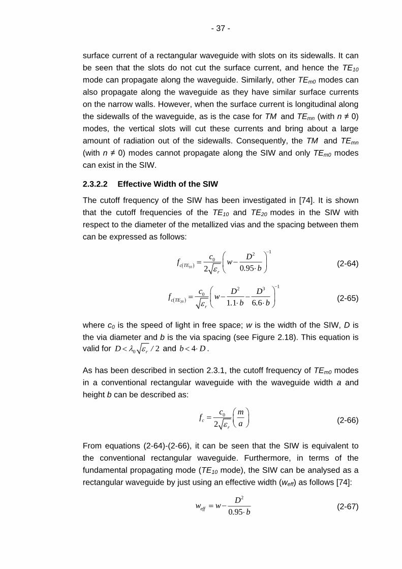
surface current of a rectangular waveguide with slots on its sidewalls. It can
be seen that the slots do not cut the surface current, and hence the TE10
mode can propagate along the waveguide. Similarly, other TEm0 modes can
also propagate along the waveguide as they have similar surface currents
on the narrow walls. However, when the surface current is longitudinal along
the sidewalls of the waveguide, as is the case for TM and TEmn (with n ≠ 0)
modes, the vertical slots will cut these currents and bring about a large
amount of radiation out of the sidewalls. Consequently, the TM and TEmn
(with n ≠ 0) modes cannot propagate along the SIW and only TEm0 modes
can exist in the SIW.
2.3.2.2 Effective Width of the SIW
The cutoff frequency of the SIW has been investigated in [74]. It is shown
that the cutoff frequencies of the TE10 and TE20 modes in the SIW with
respect to the diameter of the metallized vias and the spacing between them
can be expressed as follows:
10
12
0
0 952c TE
r
c Df w
. b
(2-64)
20
12 3
0
1 1 6 6c TE
r
c D Df w
. b . b
(2-65)
where c0 is the speed of light in free space; w is the width of the SIW, D is
the via diameter and b is the via spacing (see Figure 2.18). This equation is
valid for 0 2rD / and 4b D .
As has been described in section 2.3.1, the cutoff frequency of TEm0 modes
in a conventional rectangular waveguide with the waveguide width a and
height b can be described as:
0
2c
r
c mf
a
(2-66)
From equations (2-64)-(2-66), it can be seen that the SIW is equivalent to
the conventional rectangular waveguide. Furthermore, in terms of the
fundamental propagating mode (TE10 mode), the SIW can be analysed as a
rectangular waveguide by just using an effective width (weff) as follows [74]:
2
0 95eff
Dw w
. b
(2-67)
- 38 -
Equation (2-67) provides a good approximation between a SIW and its
equivalent rectangular waveguide. However, this approximation does not
include the effect of D/w, which may lead to small errors when D increases
[72]. To approach a better approximation, a more accurate empirical
equation to calculate the effective SIW width was proposed in [72], which
can be written as:
2 2
1 08 0 10 95
eff
D Dw w . .
. b w
(2-68)
This equation is very accurate when the requirements b / D < 3 and D / w <
0.2 are met.
2.3.2.3 Minimisation of the Losses of the SIW
One of the major issues in the design of SIW components is concerned with
the minimisation of losses. There are mainly three mechanisms of losses in
the SIW. Due to the finite conductivity of metallic walls and the loss tangent
of dielectric substrate, the SIW exhibits conductor losses as well as dielectric
losses like the conventional metallic waveguide. In addition, the presence of
gaps along the side walls of the SIW can lead to a radiation loss due to a
possible leakage through these gaps [98, 99].
The losses of the SIW can be minimized by modifying its geometrical
parameters, namely, the substrate thickness h, the via diameter D and their
longitudinal spacing b (see Figure 2.18). The thickness h of the dielectric
substrate plays an important role in the conductor loss in the SIW.
Increasing h can lead to a significant reduction of the conductor loss. This is
due to a lower electric current density flowing on the metal surface with the
increase of the thickness of substrate. The diameter of the metal vias D and
their spacing b have great influence on the radiation loss. It is shown that the
radiation leakage will become significant when the condition b / D < 2.5 is
not met [72]. Generally, the following two design rules with respect to the
metallic vias can be used to ensure the radiation losses kept at a negligible
level [100]:
D < λg / 5 (2-69)
b < 2 D (2-70)
where λg is the guided wavelength in the SIW. In this case, the SIW can be
modelled as a conventional rectangular waveguide and the mapping from
the SIW to the rectangular waveguide is nearly perfect in all the single mode
- 39 -
bandwidth. More details about the transformation from the substrate
integrated waveguide to an equivalent rectangular waveguide can be found
in literature such as [72, 73] and [100].
Finally, it is important to note that the dielectric losses of SIW structures
depend heavily on their operating frequencies [27, 99]. When the frequency
turns higher, i.e. mm-wave frequencies, the dielectric loss is typically the
most significant contribution to losses. Therefore, a proper selection of the
dielectric material is extremely important to get minimum losses for the SIWs
that work in a relatively high frequency, especially for those in the mm-wave
frequency range.
2.3.2.4 Substrate Integrated Waveguide Transition
SIW transitions play an important role in integrating SIW components with
other electronic devices. The design and implementation of transition
structures between traditional rectangular waveguides and planar circuits
have been widely studied [101-104]. Many of these structures can be
adopted for the transition between SIW structures and planar circuits directly
or with little modification, but with lower cost and more reliable fabrication
process. Furthermore, since the SIW can be integrated with planar circuits
on the same substrate, the whole circuit, including the planar circuit,
transition and SIW structures, can be constructed in a dielectric substrate
conveniently by just using a standard PCB processing technique [105].
The tapered microstrip transition [6] is one of the most commonly used
structure for the transition between the microstrip line (MSL) and SIW. As
illustrated in Figure 2.20, a microstrip line is connected directly to the top
wall of the SIW through a tapered microstrip section; the vertical
components of the electric field in both microstrip line and SIW regions are
well matched and therefore the transition can be easily achieved. The
tapered microstrip transition is a wideband structure that covers the
complete useful bandwidth of the SIW. However, if a thicker substrate is
used in SIWs in order to achieve a smaller conductor loss, the radiation loss
will increase in the microstrip line as the substrate thickness is increased.
Hence, the tapered microstrip transition is not suitable for active component
integration, especially for those at mm-wave frequencies [106].
An alternative structure for the transition between planar circuits and SIWs is
the coplanar waveguide (CPW). As shown in Figure 2.21, the CPW-SIW
- 40 -
(b)
(c)(a)
Figure 2.20 MSL to SIW transition with tapered microstrip feeding: (a) transition structure; (b) electric field distribution in SIW cross section, and (c) electric field distribution in MSL cross section
Figure 2.21 Configuration of the CPW-SIW transition
transition [107] makes use of a coplanar waveguide section to excite the
SIW, with an inset stub employed to better match the CPW and SIW. Since
increasing the height of the dielectric substrate might not have too much
influence on the inherent characteristics of CPW, this transition is less
sensitive to substrate thickness and hence exhibits a better performance
than the microstrip transition in relatively high frequencies, especially in mm-
wave frequencies. Nevertheless, it should be noted that the CPW-SIW
transition has a narrower bandwidth in comparison to the microstrip
counterpart. Several modified structures, such as the elevated CPW-SIW
transition [108], have been proposed to enhance the bandwidth performance.
2.3.3 Ridge Substrate Integrated Waveguide
Conventional ridge waveguides are well known for their advantages of low
cutoff frequency, compact size, wide bandwidth and concentration of fields in
a smaller region in the waveguide [109]. These favourable properties are
mainly achieved by the introduction of the ridge in a waveguide. As
illustrated in Figure 2.22, the main effect of the inset ridge is to produce a
capacitance at the ridge step. This capacitance will lower the cutoff
frequency of the TE10 mode in the ridge waveguide and leads to a smaller
physical size than conventional rectangular waveguides. Furthermore, since
the capacitance occurs in a low electric field region and the loading effect is
- 41 -
much less for the TE20 mode in this case, the frequency range between the
dominant mode and the first high mode is increased, and hence a wider
single-mode bandwidth is achieved [110].
Based on the concept of the ridge waveguide, the ridge SIW (RSIW) was
proposed in [111] to improve the bandwidth of SIWs by applying a metal
ridge to the SIW. As shown in Figure 2.23(a), the RSIW is built on rows of
via posts, with the central ridge realised with a row of thin metal posts. The
transmission properties of the RSIW have been studied analytically and
C C
a
bh1
h2
(a) (b)
Figure 2.22 (a) Configuration of the ridge waveguide. (b) Equivalent circuit
bottom metal layer
dielectric
substrate
metal posttop metal layer
ridge metal post
z
(a)
bottom metal layer
dielectric
substrate
metal posttop metal layer
ridge metal post
z
metal strip
(b)
Figure 2.23 (a) Configuration of the ridged SIW. (b) Configuration of the ridge SIW with a metal strip [113]
- 42 -
experimentally in [112]. It is shown that, similar to the classic ridge
waveguide, the insertion of the ridge introduces additional capacitance in the
SIW and leads to a lower cutoff frequency as well as an enhancement of the
single-mode bandwidth in comparison to conventional SIWs. Nevertheless,
due to the periodic loading of the ridge posts, it is found that this structure
exhibits a band gap when the ridge posts are thick and long. This
phenomenon reduces the useful mono-modal bandwidth of the ridge SIW,
and thus limits its utilization in the design of wideband interconnects.
A modified ridge SIW was proposed in [29, 113] to overcome this issue. As
shown in Figure 2.23(b), the modified ridge SIW is similar to the
conventional structure in Figure 2.23(a), with two side rows of full height
metal posts to form the SIW and a central row of partial-height posts to form
the ridge. Moreover, there is an additional metal strip, which connects the
ridge posts at their bottom. Owing to the presence of the metal strip, the
current density flowing in the axial direction does not experience the periodic
loading of the ridge posts and hence the band gap phenomenon is avoided.
It is shown that the modified RSIW exhibits a three times broader bandwidth
than conventional SIWs. Furthermore, the size of the modified ridge SIW is
only half of a SIW with the same cutoff frequency, thus giving significant
potential to the design of compact wideband microwave components. In the
following Chapter 3, the application of the ridge SIW in the design and
implementation of microwave filters will be studied in detail.
The configuration of the half-mode substrate integrated waveguide (HMSIW)
[30] is shown in Figure 2.24. The structure of the HMSIW is similar to that of
the SIW, but with the waveguide width half of conventional SIWs. The
HMSIW was proposed based on the approximation of the vertical cut of the
waveguide as a virtual magnetic wall [30]. As has been described in section
2.3.2, the electric field of the main mode of a conventional SIW is maximum
at the vertical centre plane along the direction of propagation; therefore, this
vertical plane can be viewed as an equivalent magnetic wall. Since half of
the waveguide will keep the half field distribution unchanged if the cutting
plane is a magnetic wall, the SIW can be bisected with this vertical centre
plane to achieve a more compact size, but with the main electromagnetic
properties of the SIW unchanged. In fact, the open side aperture of the
HMSIW is nearly equivalent to a perfect magnetic wall due to the high ratio
of the waveguide width and height [30]. Consequently, the HMSIW is
capable of achieving a size reduction of nearly 50% in comparison to
- 43 -
conventional SIWs, while keeping the main properties of the SIW.
The propagation properties of the HMSIW have been investigated in [114]. It
is shown that only TEp-0..5, 0 (p = 1, 2, …) modes can propagate in the
HMSIW due to the large width-to-height ratio of the HMSIW and the discrete
arrangement of metallic vias. The dominant mode in the HMSIW is the
TE0.5,0 mode. The electric field distribution of the TE0.5,0 mode in the HMSIW
is shown in Figure 2.24(c). It can be seen that the electric field distribution is
similar to half of the fundamental TE10 mode in the conventional SIW. This is
also why it is termed the half-mode SIW.
The cutoff frequency of the main mode of the HMSIW (TE0.5,0 mode) can be
calculated by [114]:
0 5 0
0
4. ,c TE
r eff _ HMSIW
cf
w (2-71)
(a)
(b)
(c)
Figure 2.24 (a) Top view of the configuration of the HMSIW. Dark grey shading represents metallization. (b) Side view of the configuration of the HMSIW. (c) Electric field distribution of the TE0.5,0 mode in the HMSIW [114]
- 44 -
where eff _ HMSIWw represents the equivalent width of the HMSIW, which can
be expressed as:
2 2
2
3 2
0 54 0 052
104 2610 3 380 05 0 79 2 77
'
eff ,HMSIW eff ,HMSIW
'
eff ,HMSIW
' '
eff ,HMSIW eff ,HMSIW
r
W W W
d dW w . .
s w
W WW .. ln . .
h h h h
(2-72)
where w is the width of the HMSIW, h is the height of the HMSIW, d is the
via diameter, and s is the via spacing.
For the first high mode TE1.5,0 mode, the cutoff frequency can be
approximated as:
1 5 0
03
4. ,c TE
r eff _ HMSIW
cf
w (2-73)
From equations (2-71)-(2-73), it can be seen that the cutoff frequency of the
first higher mode is three times that of the fundamental mode in the HMSIW.
Therefore, if not considering the suppression of the high modes, a HMSIW
with a width w has a single-mode operation frequency range approximately
twice that of a SIW with a width 2w [114].
As described above, the electric field distribution of the main mode of the
HMSIW is similar to half of the fundamental TE10 mode in conventional SIWs
[114]. Since the ridge SIW is capable of achieving a more compact size in
comparison to conventional SIWs by loading the SIW with a ridge (see
section 2.3.3), it may be possible to load the HMSIW with a ridge like the
ridge SIW to achieve a further size reduction, while keeping the main
advantages of the HMSIW. This solution to reduce the size of HMSIWs will
further be studied in detail in Chapter 4.
- 45 -
2.3.5 SIW with the Complementary Split Ring Resonator (CSRR)
The configuration of the edge-coupled split ring resonator (EC-SRR) was
initially proposed by Pendry et al. in [39]. As shown in Figure 2.25(a), the
EC-SRR is formed by two concentric conducting rings printed on a dielectric
substrate. These two split rings are coupled by means of a strong distributed
capacitance between the rings. If a time varying magnetic field is applied
parallel to the rings axis, current loops will be induced in the rings and these
current lines will pass from one ring to the other through the distributed
capacitance between the rings. Therefore, the EC-SRR behaves as a
parallel LC resonant tank that can be excited by external magnetic fields,
and its resonant frequency frs can be expressed as [115]:
1
2rs
s s
fL C
(2-74)
where Ls and Cs are the total inductance and capacitance of the EC-SRR,
respectively.
LsCs
(a)
LcCc
(b)
Figure 2.25 (a) Configuration of the EC-SRR and the equivalent circuit. (b) Configuration of the EC-CSRR and the equivalent circuit. Dark Grey represents metallization
- 46 -
A detailed procedure to calculate the value of Ls and Cs has been given in
literature [49, 115]. It is shown that the inductance and capacitance of the
EC-SRR are mainly governed by the ring width (c) and the spacing between
the rings (d), respectively. The decrease of c / d can result in a larger Ls / Cs
and further lead to a lower resonant frequency and a more compact size.
However, it should be noted that very intense electric fields could appear at
the ring edges for the EC-SRR with very small spacing, which may cause
high losses and/or dielectric breakdown. Hence, these effects should be
taken into account when the EC-SRR is used to implement microwave
components with very small physical size.
From a duality argument, the edge-coupled complementary split ring
resonator (EC-CSRR) was proposed by Falcone et al. in [41]. As shown in
Figure 2.25(b), the EC-CSRR is the negative counterpart of the EC-SRR. It
can be modelled as a resonant LC tank driven by external electric fields. The
resonant frequency of the EC-CSRR (fcr) is given by [115]:
1
2rc
c c
fL C
(2-75)
where Lc and Cc are the total inductance and capacitance of the EC-CSRR,
respectively. For relatively thick substrate, frc can be approximated with the
resonant frequency of the corresponding EC-SRR (see (2-74) ) from the
duality concept [41]. However, more accurate calculation of the value of frc
as well as the related Lc and Cc can be found in the literature [115].
The combination of SRRs/CSRRs and a rectangular waveguide has been
investigated in several papers such as [43-45]. It is shown that the SRRs
and CSRRs are capable of generating a passband below the cutoff
frequency of the waveguide or a sotpband above the cutoff frequency. This
property can be interpreted as a result of the negative
permeability/permittivity introduced by SRRs/CSRRs in the waveguide [43,
44]. However, from another perspective, it is demonstrated that the
passband below the cutoff frequency is caused by the properties of the
periodical array of resonator dipoles, and for other electric scatterers that are
realised with inductively loaded short wires or strips, they can also be
suitable for implementation of miniaturized waveguide in a similar way to the
SRRs and CSRRs [116, 117].
Several miniaturized waveguide filters have been developed making use of
the special properties of SRRs and CSRRs [31]. Particularly, since the
- 47 -
CSRR can be integrated into the SIW conveniently by just etching CSRRs
on the top/bottom broadwalls of the SIW, a great deal of attention has been
paid on its application to the design of miniaturized SIW filters. For example,
in [31], novel compact SIW bandpass filters loaded by CSRRs were
proposed by using the passband below the cutoff frequency of the SIW. In
[48, 52], wide-band SIW bandpass filters were proposed by combining the
stopband of periodical CSSRs with the high-pass band of the SIW. However,
it should be noted that most of these filters were implemented with
conventional EC-CSRRs. Since the size reduction of the EC-CSRR is similar
to that of the EC-SRR, which is mainly through the decrease of the spacing
between the rings of the EC-CSRR, the compactness of these filters is
limited by fabrication techniques as well as potential high losses and
dielectric break [49]. Furthermore, for the bandpass filters that are realised
by combing the high-pass band of SIWs and stopband of EC-CSRRs (such
as the filter presented in [48]), since the bandwidth of conventional EC-
CSRRs is relatively narrow, this type of filters has a relatively narrow
stopband and the out-of-band rejection may be insufficient for some
applications. Hence, novel structures are needed to improve the
compactness and stopband performance of these filters.
Recently, two new types of resonators that exhibit improved compactness
and out-of-band performance in comparison to conventional EC-SRRs and
EC-CSRRs have been proposed: the broadside-coupled split ring resonator
(BC-SRR) [50] and the complementary electric-LC (CELC) resonator [118].
The configuration of the BC-SRR is shown in Figure 2.26(a). It can be seen
that the BC-SRR can be derived from the EC-SRR (see Figure 2.25(a)) by
replacing one of the rings by another ring located just at the opposite side of
the dielectric substrate, with the slits still placed at opposite sides. The
electromagnetic properties of the BC-SRR are similar to that of the EC-SRR.
It can be modelled as a resonant LC circuit driven by proper magnetic field.
However, compared to conventional EC-SRRs, the BC-SRR has a more
compact size due to a higher capacitance that can be obtained for the
broadside-coupled metallic strips [50]. Making use of this property, it may be
possible to develop a new broadside-coupled complementary split ring
resonator (BC-CSRR) with smaller size than conventional EC-CSRRs by
using the duality concept, and apply the new BC-CSRR resonator for the
realisation of miniature SIW filters.
- 48 -
(a) (b)
Figure 2.26 (a) Configuration of the BC-SRR. (b) Configuration of the CELC resonator
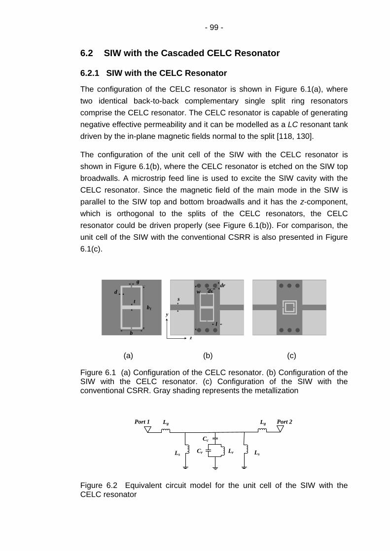
The configuration of the CELC resonator is shown in Figure 2.26(b). The
CELC resonator is composed of two identical back-to-back complementary
single split rings and it can be modelled as a resonant LC tank driven by the
in-plane magnetic fields normal to the split. When etched on the ground
plane of microstrip lines, it is found that the CELC resonator is capable of
generating a broad stopband with two transmission zeros due to its magnetic
and electric resonances [42]. Taking advantage of this property, it may be
possible to adopt the CELC resonator in SIW filters to achieve improved out-
of-band performance. More detailed studies on the application of the BC-
SRR and the CELC resonator in SIW filters will be presented in Chapters
5&6.
2.4 Summary
In this chapter, an overview of microwave filters and substrate integrated
waveguide has been presented.
Sections 2.1 & 2.2 present an outline of microwave filters and the filter
design method, including the approximation of transfer functions, synthesis
of the lowpass filter prototypes and frequency and impedance
transformations. Filter prototypes with immittance inverters are also
discussed.
In section 2.3, an overview of the substrate integrated waveguide has been
presented. The basic concepts and design rules of the SIW have been
discussed, including the propagating wave, the equivalent waveguide width,
and the miniaturized losses of SIWs. The SIW transition has been briefly
considered. Several modified SIW configurations such as the ridge SIW,
half-mode SIW and SIW with complementary split ring resonators have been
presented.
- 49 -
Chapter 3
Ridge Substrate Integrated Waveguide Filters
3.1 Introduction
As described in Chapter 2, the ridged SIW is an integrated waveguide
structure which is based on the configuration of the conventional ridged
waveguide [33, 109] by using rows of periodic metallised via holes to
approximate the vertical solid walls of the waveguide and the ridge [28, 113].
The ridged SIW has a lower cutoff frequency and wider single mode
bandwidth in comparison to the conventional SIW. Therefore, it has great
potential in the design of filters with compact sizes and wide rejection band.
Several compact filters based on the ridged SIW implemented in LTCC
technology, where the ridge is realised by printing top and bottom broadwalls,
and rows of metal-filled vias for the sidewalls, have been proposed in [35].
However, it should be noted that the ridged SIW filters might be also
possible to be realised in multilayer PCB technology, which could lead to the
integration of ridge waveguide filters into normal PCB subassemblies and
further avoid the time consuming and comparatively high cost manufacturing
technique of LTCC.
In this chapter, attention will be paid to the design and implementation of a
ridged SIW bandpass filter based on the multilayer PCB technology. An
efficient design approach of the ridged SIW bandpass filter is proposed.
Initially, the bandpass filter is designed as a conventional ridged waveguide
filter configuration with ideal solid walls so that the dimensions of the ridge
can be roughly determined to meet a specific frequency response. Then, by
using the metallised via-fence wall to emulate the solid walls, the previous
filter configuration is transformed to a ridged SIW bandpass filter which can
be realised with multilayer PCB technology. A prototype of the ridged SIW
bandpass filter was designed according to this proposed design approach
and fabricated using the multilayer PCB. The experimental measurement
agrees well with the simulation on the frequency response. It is
demonstrated that the ridged SIW bandpass filter can be implemented using
the multilayer PCB technology with easy fabrication and low cost, while
keeping the advantages of compact size and high integration.
- 50 -
3.2 Design of the Ridged SIW Filter
3.2.1 Design of the Ridged SIW Resonator
The configuration of a ridged SIW resonator is shown in Figure 3.1. Two-
rows of metallised vias (the bolder vias shown in Figure 3.1) are used to
form the sidewalls of the SIW cavity. The ridge is also realised by periodic
metallic via holes (the smaller via holes in the central region shown in Figure
3.1) where an additional metallic plane is used to connect the via holes on
the bottom. However, these vias of the ridge do not go through the entire
dielectric substrate – which is why multilayer technology is required.
Inevitably, the multilayer ridged SIW can only be realised with a small
number of different ridge height values, and this has to be taken into account
in the design and optimization of the structure. A microstrip feed line is used
at the input and output of the cavity. As ridged waveguides are often used
for waveguide to microstrip transitions, this guarantees that the ridged SIW
cavity is properly excited.
s
w
l1d2
ds3
ds2
ds1
d1
metallic vias to emulate
solid metallic walls
dielectric substrate metallic plane
microstrip
feedlineridge
(a) (b)
εr
h1
h2
εr
εr
εr
h
h
h
(c) (d)
Figure 3.1 Configuration of the ridged SIW resonator: (a) 3-D view; (b) top view; (c) side view for a resonator in a 2-layer board with different substrate height, and (d) side view for a 3-layer board with equal substrate heights
- 51 -
To aid the design of the ridged SIW resonator with specific frequency
responses, an initial ridged waveguide resonator configuration with ideal
solid metal walls and filled with the same homogeneous dielectric substrate
as the ridged SIW resonator was first designed (see Figure 3.2). The design
of this configuration can be conveniently conducted in reference to the
classic ridged waveguide theory [33]. This ridged waveguide resonator
configuration could then be converted to the ridged SIW resonator by using
periodic metallised vias to emulate the vertical solid walls (i.e. from Figure
3.2(a) to Figure 3.1(a)). However, it should be noted that the width of the
ridged SIW resonator (w) is slightly different from that of the initial ridged
waveguide resonator (w1) due to the introduction of the via-fence wall. The
width of the ridged SIW resonator could be approximated with that of the
ridged waveguide configuration with ideal solid walls by using the following
equation [119]:
2
11
10 95
dw w
. ds
(3-1)
where w and w1 denote the width of the ridged SIW and the ridged
waveguide respectively; d1 and ds1 represent the via diameter and the via
dielectric substrate
metallic ridge
metallic enclosure
microstrip feedline
(a)
s1
w1 w2
l3 l2εr
h1
h2
(b) (c)
Figure 3.2 Configuration of the ridged waveguide resonator: (a) 3-D view; (b) top view; (c) side view
- 52 -
pitch, respectively (see Figure 3.1(b) and Figure 3.2(b)). Similar to the row of
metallised via holes forming the SIW side-walls, the side walls of the SIW
ridge are also realised with a row of metallised via holes. To achieve a better
approximation to the ideal vertical walls of the ridged waveguide
configuration, the distance between two adjacent via centres, i.e. the via
hole pitch, is chosen to be [120]:
ds1≤ 2 d1 (3-2)
ds2≤ 2 d2 (3-3)
ds3≤ 2 d2 (3-4)
where d1 and d2 denote the diameters of the vias forming the SIW wall and
the SIW ridge, respectively; ds1 represents the via hole pitch of the SIW wall;
and ds2 and ds3 represent the via hole pitch of the SIW ridge (see Figure
3.1(b)).
By using the ridged waveguide resonator configuration and the design
principles described in (3-1)-(3-4), the initial dimensions of the ridged SIW
resonator can be obtained. However, since the sidewalls of the SIW ridge
are implemented by using a via fence to approximate the vertical solid wall,
the effect of this via-fence wall should be taken into consideration and some
tuning and optimization need to be carried out in order to get a better
equivalent of the required ideal resonator configuration. Figure 3.3(a)-(c)
present the HFSSTM simulated results of a single resonator with different via
diameters (d2) and via hole pitches (ds2, ds3) of the SIW ridge, respectively.
It can be seen that the resonant frequency shifts higher with the increase of
d2 and ds2 (see Figure 3.4(a)-(b)), and shifts lower with the increase of ds3
(see Figure 3.4(c)). This change of the resonant frequency is because the
change of d2, ds2 and ds3 results in a different equivalent size of the ridge.
Moreover, Fig. 4(d) presents the response of the resonator for different
values of the height of the ridge h1. It can be seen that the resonant
frequency is significantly reduced when h1 increases, and higher selectivity
is also observed. This is due to the increase of the loading capacitance with
the increased height of the ridge, h1 [121]. This indicates that a more
compact size and better performance could be achieved by choosing a large
h1 or the ratio h1/h2.
- 53 -
By looking at these simulations with swept parameters, optimal dimensions
of the ridged SIW resonator can be determined. Figure 3.4 displays the
transmission response of one such design. A ridged waveguide resonator
was initially designed to achieve a resonant frequency at 9.26 GHz, with the
parameters as follows: εr = 2.65, h1 = h2 = 1 mm, s1 = 3 mm, w1 = 9 mm, w2 =
5.3 mm, l2 = 4 mm, l3 = 4.45 mm. By the design approach discussed above,
an equivalent ridged SIW resonator was designed with the parameters as
follows: εr= 2.65, h1 = h2 = 1 mm, s = 3 mm, w = 10.05 mm, l1= 4.75 mm, d1=
1.6 mm, d2= 1.2 mm, ds1= 2.9 mm, ds2 = ds3 = 2 mm. From Figure 3.4, it can
be seen that excellent agreement is achieved between the frequency
response of the ridged SIW resonator and that of the ridged waveguide
resonator configuration.
(a) (b)
(c) (d)
Figure 3.3 Simulated frequency responses of the ridged SIW resonator with: (a) different via diameter d2 (with h1 = 1 mm); (b) different via hole pitch ds2 (with h1 = 1 mm); (c) different via hole pitch ds3 (with h1 = 1 mm); (d) different height of the ridge h1 (with parameters εr = 2.65, h1 = h2 = 1 mm, s = 3 mm, w = 10.05 mm, l1= 4.75 mm, d1= 1.6 mm, d2= 1.2 mm,ds1= 2.9 mm, ds2= 2 mm, ds3= 2.2 mm)
- 54 -
S21 S11
Figure 3.4 Simulated frequency responses of the ridged SIW resonator and the ridged waveguide resonator configuration
To physically realise the ridged SIW resonator, it is feasible to use multilayer
PCB technology. For example, in Figure 3.1(c), the ridged SIW resonator
can be conveniently constructed out of two-layer dielectric substrate, with
the thickness of top substrate h1 equal to that of ridges, and the thickness of
bottom layer h2 representing the gap between the ridge and bottom ground
plane. By properly choosing the thickness of top substrate, h1, and bottom
substrate, h2, better performance and more compact size can be achieved
as discussed before. On the other hand, it is also feasible to build the
resonator by using a multilayer substrate with each layer having the same
thickness. In this case, the vertical walls of the ridge can be realised with
metallised via holes through several layers of the substrate. As shown in
Figure 3.1(d), for example, the ridged SIW resonator can be realised in a
three-layer dielectric substrate with the thickness of each layer being h; the
vertical walls of the ridge are then formed from the metallised vias through
the first and second layer, with the third layer forming the gap between the
ridge and the bottom ground plane. In terms of this method of physical
realization, although the height of the ridge is restricted to a limited set of
discrete values, multilayer boards often have 18 or more layers, allowing
sufficient design freedom.
From these discussions, it can be seen that there is great flexibility in the
design and physical realis ation of the ridged SIW resonator. The design
methodology starts with a conventional ridged waveguide resonator
configuration with ideal solid walls and then converts it to the ridged SIW
counterpart. The implementation of the ridged SIW resonator is convenient
- 55 -
and flexible, which can lead to the easy integration of ridged SIW
components with other circuits.
3.2.2 Design of the Ridged SIW Bandpass Filter
A bandpass filter with a bandwidth 0.6 GHz at a center frequency 9.24 GHz
was designed based on the ridged SIW resonator. The ridged SIW
bandpass filter consists of ridged SIW resonators coupled by evanescent-
mode SIW sections. Based on the design strategy mentioned above, an
initial ridged waveguide bandpass filter configuration with dielectric constant
= 2.65 and the height of each layer 1 mm (h1 = h2 = 1 mm), was first
designed. As shown in Figure 3.5(a) and Figure 3.5(b), the ridged
resonators with ideal vertical walls which are coupled by sections of the
evanescent-mode waveguide. An inset microstrip transition was employed to
get a better match between the cavity and the microstrip feed line.
A third order (n = 3) Chebyshev lowpass prototype with a passband ripple of
0.1 dB is chosen for the design of the ridge waveguide filter. The lowpass
prototype parameters, given for a normalized lowpass cutoff frequency Ωc =
1, are g0 = g4 = 1, g1 = g3 = 1.035, g2 = 1.147. Having obtained the lowpass
parameters, the bandpass design parameters can be calculated by [1]:
0 1 11 1
1 1 1 1
n ne e
i ,i i i
g g g gQ Q
FBW FBW
k FBW / g g for i to n
(3-5)
where FBW is the fractional bandwidth, Qe1 and Qen are the external quality
factors of the resonators at the input and output, and ki,i+1 are the coupling
coefficients between the adjacent resonators.
For this design example, we have: Qe1 = Qe3 = 15.4; K1,2 = k2,3 = 0.1097.
Using a parameter-extraction technique described in [2], the relationship
between the external factor Q, coupling coefficient k and the physical
dimensions can be obtained. The external Q factor can be extracted by
using a doubly-loaded resonator and calculated by:
20
3
fQe
fdB
(3-6)
where f0 is the frequency where S21 is maximum; ∆f3dB denotes the 3-dB
bandwidth for which S21 is reduced by 3 dB from the maximum value.
- 56 -
The coupling coefficients can be obtained using [2]:
2 2
1 2
2 2
1 2
f fk
f f
(3-7)
where f1 and f2 represent the resonance frequencies of low and high modes,
respectively. Figure 3.5(e) shows the value of coupling coefficient k against
the evanescent-mode waveguide coupling length (denoted by l) between two
adjacent ridge waveguide resonators. It can be seen that the coupling
between resonators increases with the decrease of the evanescent-mode
waveguide length.
After getting the initial dimensions of the ridge waveguide filter, the
parameters of the filter can be tuned to get a better result. The centre
frequency of the filter can be adjusted by tuning the length of the ridge l’5 and
l’7 (see Figure 3.5(a)). The bandwidth of the filter can be tuned by changing
the length of the evanescent-mode SIW sections l’4 and l’6. The parameters
of the transition, such as s’2, l
’2 and l’3, can be tuned to get a better match
between the feed line and the ridge waveguide. The dimensions of the ridge
waveguide filter are presented in Table 3.1.
After obtaining the initial ridged waveguide filter configuration, this ridged
waveguide filter configuration was then converted to the ridged SIW filter by
employing periodic via holes. The dimensions of the ridged SIW filter were
approximated by using (3-1)-(3-4). To achieve an optimal approximation,
parametric analysis and optimization of the filter were carried out with
HFSS™. Figure 3.5(c)-(d) shows the layout of the designed ridged SIW filter,
with the dimensions of the ridged SIW filter presented in Table 3.2. The
simulated responses of the ridged SIW filter and the ridged waveguide filter
configuration with ideal solid walls are compared in Figure 3.6. Similarly to
the resonator, very good agreement was achieved between the frequency
response of the ridged SIW filter and the ridged waveguide filter.
- 57 -
w1w2
l1’l2
’l3’ l4
’ l5’ l6
’ l7’
εr
h1
h2
s1’ s2
’
(a) (b)
s1 s2
l1 l2
l3 l4
ds3ds2
ds1
ds4
w
d1
d2
εr
h1
h2
(c) (d)
(e)
Figure 3.5 (a) Top view and (b) side view of the conventional ridged waveguide filter configuration; (c) top view and (d) side view of the ridged SIW filter; (e) the coupling coefficient k as a function of the length of the evanescent-mode coupling waveguide l (with h1 = h2 = 1 mm).
Table 3.1 Parameters of the initial ridged waveguide filter configuration (unit: mm)
s’1 s
’2 w1 w2 l
’1 l
’2 l
’3 l
’4 l
’5 l
’6 l
’7
3.5 4.4 9.05 5 5 6.2 2.5 5.2 4 11 4
Table 3.2 Parameters of the ridged SIW filter (unit: mm)
s1 s2 w l1 l2 l3 l4 d1 d2 ds1 ds2 ds3 ds4
3 4 10.
25
5 5 5.3 11.
5
1.6 1.2 2.9 1.9 2 2
- 58 -
S21
S11
Figure 3.6 Simulated frequency responses of the ridged waveguide filter configuration and the ridged SIW filter
Figure 3.7 Photograph of the ridged SIW filter
3.3 Fabrication and Measurement
To verify the simulated results, the ridged SIW bandpass filter was fabricated
on a two-layer F4B-1/2 dielectric substrate with dielectric constant r = 2.65,
loss tangent of the dielectric substrate tanδ = 0.001, and the height of each
layer being 1 mm. A photograph of the fabricated filter is shown in Figure 3.7.
The frequency response of the filter was measured using an Agilent E8363A
network analyzer. Figure 3.8 shows the simulated and measured frequency
responses of the filter over the 8 to 11 GHz band. The measured centre
frequency and 3-dB bandwidth are 9.24 and 0.6 GHz, respectively. The
measured in-band return loss is below -13 dB, while the insertion loss is 3.5
dB including the feed lines and SMA connectors.
- 59 -
S21
S11
Figure 3.8 Simulated and measured frequency responses of the ridged SIW filter
3.4 Summary
In this chapter, the design and performance of a ridged SIW bandpass filter
implemented by multilayer PCB are presented. The design and physical
realisation of the ridged SIW resonator is first investigated, and then the
ridged SIW bandpass filter is implemented on cascaded resonators coupled
by evanescent-mode SIW sections. A methodology is proposed to design
the ridged SIW bandpass filter. The design methodology starts from a ridged
waveguide filter configuration with solid walls, and then the solid walls are
converted to metallic via-fence. One prototype of the ridged SIW bandpass
filter is fabricated using multilayer PCB technology and measured. The
measured results agree well with the simulations. It is shown that ridged SIW
bandpass filter can be efficiently designed with the proposed design
methodology and realised with standard multilayer PCB technology which is
comparatively convenient and inexpensive. The ridged SIW bandpass filter
has the advantages of compact size, low cost and easy integration with
other components and circuits, and thereby it has significant potential for use
in microwave and millimetre wave systems.
- 60 -
Chapter 4
Compact Ridge Half-Mode SIW Filters
4.1 Introduction
As described in Chapter 2, the half-mode SIW (HMSIW) is a type of modified
SIW structure which is realised by approximating the vertical cut of the SIW
as a virtual magnetic wall (see Figure 4.1(a)) [37]. The HMSIW is nearly half
the size of the conventional SIW but still keeps the main advantages of the
SIW. Compact filters based on the HMSIW, which exhibit more compact size
and wider stopband in comparison to the conventional SIW filters, have been
proposed in [37, 38]. However, the size of these filters may be still too large
for some applications, especially for those operating at a relatively low
frequency. From the discussion in the previous chapter, we know that the
ridge SIW is capable of achieving a more compact size in comparison to
conventional SIWs by loading the SIW with a ridge (see Figure 4.1(b)). Since
the electromagnetic field distribution of the main mode of the HMSIW is
similar to half of the main mode of the SIW [37], it may be feasible to load
the HMSIW with a ridge like the ridged SIW to achieve a further size
reduction, while keeping the main advantages of the HMSIW.
In this chapter, a ridged half-mode substrate integrated waveguide
(RHMSIW) is proposed and investigated by integrating a ridge into the
HMSIW. It is shown that the RHMSIW demonstrates a lower cutoff
frequency and a more compact size compared to conventional HMSIW as
additional capacitance is produced by the ridge. Based on the RHMSIW, a
compact wideband bandpass filter with directional coupling is designed and
fabricated on multilayer PCB.
metallic vias
dielectric
substratemetallic plane
metallic vias
dielectric
substratemetallic plane
ridge
(a) (b)
Figure 4.1 (a) 3-D view of the HMSIW. (b) 3-D view of the ridge SIW
Figure 4.2 shows the proposed configuration of the RHMSIW, where a ridge
is integrated into a HMSIW. The vertical solid walls of the ridge are realised
with periodic metallic vias. The bottom surface of the ridge is a metal strip
which connects these vias, and the top surface of the ridge overlaps with
that of the HMSIW. A microstrip feed line is used at the input and output of
the cavity, with a transition employed to better match the RHMSIW and the
microstrip feed line. As ridge waveguides are often used for waveguide to
microstrip transitions, the RHMSIW cavity is properly excited.
metallic vias
dielectric
substrate
ridge
metallic plane
microstrip
feedline with
transition
metal strip
(a) a
h1
h2
Layer1
Layer2
ds
s1
dr
s2
l1 l2 ds1dr1
w
w1
εr
(b) (c)
Figure 4.2 Configuration of the RHMISW: (a) 3-D view; (b) top view and (c) side view
Cd Cp
L Cp Cd L C
(a) (b)
Figure 4.3 (a) The capacitance for a unit length of the RHMSIW at the cutoff frequency of the main mode. (b) Equivalent circuit model for a unit length of the RHMSIW at the cutoff frequency of the main mode
- 62 -
The main effect of the ridge in the RHMSIW is similar to that in the ridged
SIW and the conventional ridged waveguide; it introduces additional
capacitance and leads to a lower cutoff frequency for a given physical size
[109]. As shown in Figure 4.3(a), the capacitance of the RHMSIW is mainly
composed of two parts: the electrostatic, parallel-plate capacitance between
the ridge and the bottom ground plane (Cp), and the discontinuity
capacitance at the bottom corners of the ridge (Cd). Generally, the
capacitance introduced by Cp is more significant than Cd. The value of Cp
and Cd are dependent on the ratio h1/h2 and the width of the ridge, w,
thereby the loading capacitance can be tuned by changing these dimensions
of the ridge.
Similar to the conventional ridged waveguide [33, 109, 122], the cutoff
frequency of the RHMSIW can be approximated by a simplified equivalent
circuit. As shown in Figure 4.3(b), in terms of the cutoff frequency of the
main mode, the RHMSIW can be modelled as a parallel LC tank, where the
inductance L represents the inductance of the per unit length of the
waveguide, which indicates the path that the current flow through; and the
capacitor C represents the capacitance between the ridge and the
waveguide. The cutoff frequency (fc) of the main mode of the RHMSIW can
then be approximated with the resonant frequency of the shunt-connected
LC tank, namely:
1
2cf
LC (4-1)
where the capacitance C can be expressed by:
C = Cp + Cd (4-2)
From equations (4-1) and (4-2), it can be seen that as a larger parallel-plate
capacitance (Cp) and an extra discontinuity capacitance (Cd) is introduced in
waveguide by loading a ridge, the RHMSIW exhibits a lower cutoff frequency
in comparison to the conventional HMSIW.
An example of the RHMSIW was designed and investigated with the
parameters (see Figure 4.2) chosen as follows: εr = 2.65, h1 = h2 = 0.5 mm,
s1 = 2.2 mm, s2 = 4.6 mm, l1 = 5.3 mm, l2 = 6.4 mm, dr = 1.1 mm, ds = 2 mm,
dr1 = 1 mm, ds1 =1.85 mm, a = 7.85 mm, w = 3.7 mm, w1 = 5.2 mm. It is
important to notice that the distance between two adjacent vias (the via hole
pitch, denoted by ds and ds1 in Figure 4.2) should be less than twice of the
diameter of the via (dr and dr1) to achieve a better approximation to the ideal
- 63 -
vertical walls [123]. The frequency responses of the RHMSIW were
simulated by the HFSSTM and the results are presented in Figure 4.4. A
good high-pass response with a cutoff frequency of 4 GHz is observed. For
comparison, the simulated frequency response of the conventional HMSIW
with the waveguide dimensions identical to that of the RHMSIW was also
investigated and plotted in Figure 4.4. As expected, the cutoff frequency of
the HMSIW, which is at 6.5 GHz, is much higher than that of the RHMSIW (4
GHz). For a conventional HMSIW with the cutoff frequency of the main mode
at 4 GHz, the width of the waveguide needs to be 11.8 mm, and this is much
wider than that of the RHMSIW (7.85 mm). Therefore, the RHMSIW is more
compact compared to the conventional HMSIW. Furthermore, since the
loading capacitance between the ridge and the bottom ground plane of the
waveguide (Cp) increases with the increase of the height of the ridge (h1) and
the decrease of the height of the gap between the ridge and the bottom
ground plane (h2), a further size reduction could be achieved for the
RHMSIW by increasing the ratio h1/h2 appropriately.
To better understand the structure of the RHMSIW, the electric field
distribution of the main mode in the RHMSIW was also investigated. As
depicted in Figure 4.5(a), the electric field of the RHMSIW is similar to that of
the HMSIW and the ridge SIW, being basically perpendicular to the bottom
ground plane and reaching the maximum near the open aperture. By
comparing the E-field distribution of the main mode of the RHMSIW with that
Figure 4.4 Simulated frequency response of the RHMISW, compared with the HMSIW with identical waveguide dimensions, and the ridge SIW with the width of the waveguide and the ridge twice that of the RHMSIW
- 64 -
of the ridged SIW, with the width of the waveguide and the ridge twice that of
the RHMSIW (see Figure 4.5(b)), it can be seen the electric field distribution
of the RHMSIW is quite similar to half that of the ridged SIW. This is not
unexpected. Since the electric field of the main mode of the ridge SIW is
basically orthogonal to the bottom broadwall of the waveguide and it is
maximum at the vertical centre plane of the bottom layer, this vertical centre
plane along the direction of propagation could be approximated as a virtual
magnetic wall (see the inset of Figure 4.5(b)). Therefore, the RHMSIW could
be viewed as half of the ridged SIW which is bisected with this virtual
magnetic wall. Furthermore, due to the large width-to-height ratio, the
dominant mode field distribution and propagation characteristics of the
RHMSIW are similar to that of the ridge SIW. Figure 4.4 presents the
simulated frequency responses of the ridged SIW with the width of the
waveguide and the ridge twice that of the RHMSIW. It can be seen that the
cutoff frequency of the ridged SIW is at 4.12 GHz, which is quite close to that
of the RHMSIW (4 GHz). This also indicates that the proposed RHMSIW
works similarly to the ridge SIW but with the physical size reduced to half.
wa
(a)
2a2w
vertical center plane approximated as a
virtual magnetic wall
(b)
Figure 4.5 Electric field distribution of the main mode in the: (a) RHMSIW and (b) ridged SIW with the width of the waveguide and the ridge twice that of the RHMSIW
- 65 -
Based on the analysis above, in the design of a practical device with the
RHMSIW, the width of a conventional ridged waveguide with vertical solid
walls and working in the same frequency could be determined firstly with the
classic theory of ridged waveguide [33, 122]. This ridged waveguide can
then be converted into a ridged SIW by using periodic via holes to replace
the vertical solid walls. The design rules for the via holes shown in [72, 112,
123] could be used to achieve a better approximation to the ideal vertical
walls, namely:
ds ≤ 2 dr (4-3)
ds1 ≤ 2 dr1 (4-4)
where dr and ds are the diameter of the vias forming the waveguide and the
via pitch, respectively; dr1 and ds1 are the diameter of the vias forming the
ridge and the via pitch, respectively (see Figure 4.2). The width of the
RHMSIW is then approximately half that of the ridged SIW, which could be
used as initial dimensions for the design of the RHMSIW.
4.3 Compact Wideband Bandpass Filter with the RHMSIW
Based on the configuration of the RHMSIW, a compact wideband RHMSIW
bandpass filter with directional coupling was designed and simulated with
HFSSTM. The layout of the RHMSIW bandpass filter is shown in Figure
4.6(a)-(b). The filter is directly coupled by the HMSIW sections. A transition
was used to better match the RHMSIW and the microstrip feed lines. The
initial dimensions of the RHMSIW can be approximated by half of the ridge
waveguide working in the same cutoff frequency, as described in section 4.2.
The centre frequency of the filter can be adjusted by tuning the parameters
dr1 and ds1, which are relevant to the equivalent length of the ridge. The
coupling between resonators can be tuned by changing the length of the
HMSIW sections, l4 and l6. The parameters of the filter after tuning are
shown in Table 4.1.
A two-layer F4B-1/2 dielectric substrate was used to fabricate the filter with
dielectric constant εr = 2.65, the loss tangent of the dielectric substrate tanδ
= 0.001, and the thickness of upper layer and lower layer being 1 mm and
0.5 mm, respectively. Figure 4.6(c) shows a photograph of the fabricated
RHMSIW filter. The filter was measured with an Agilent E8363A network
analyzer.
- 66 -
ds
s1s2
l2l1
ds1dr1dr
l4 l6l3 l5
(a)
a
h1
h2
Layer1
Layer2
w
w1 εr
(b)
(c)
Figure 4.6 (a) Top view showing the layout of the wideband RHMSIW filter. (b) Cross-sectional view of the filter. (c) Photograph of the fabricated filter
Table 4.1 Parameters of the RHMSIW filter (unit: mm)
εr h1 h2 s1 s2 l1 l2 l3 l4 l5 l6 dr
2.65 1 1 2.5 4.1 5.3 7.6 2.8 3.75 4.8 1.8 1.1
ds dr1 ds1 a w w1
2.1 1 1.87
.85
7.85
5
3.6 4.8
S11
S21
Figure 4.7 Simulated and measured frequency responses of the wideband RHMSIW filter
- 67 -
The measured and simulated frequency responses of the filter are depicted
in Figure 4.7. Good agreement is achieved between the measurement and
the simulation. The measured centre frequency and 3-dB bandwidth are
6.47 and 4.9 GHz, respectively. The measured in-band return loss is better
than 18 dB. The insertion loss is 1 dB including the feed lines and SMA
connectors. The size of the filter is only 18.3 mm × 8.4 mm × 1.5 mm without
the feed line. Moreover, by using a thicker dielectric substrate for the ridge or
a thinner dielectric substrate for the gap between the ridge and the bottom
ground plane, the size of the filter could be further reduced.
4.4 Summary
In this chapter, the design and performance of a compact wideband filter
based on the RHMSIW (ridged half-mode substrate integrated waveguide)
are presented. The proposed RHMSIW shows a lower cutoff frequency and
a more compact size compared to the conventional HMSIW due to the
additional capacitance introduced by the loaded ridge. Further physical size
reduction could be achieved for the RHMSIW by increasing the height of the
ridge or decreasing the gap between the ridge and the bottom ground plane
appropriately. A compact wideband bandpass filter with the RHMSIW has
been designed and fabricated. Good agreement has been achieved between
the measurement and the simulation. The proposed filter is compact, low
loss, easy to fabricate and integrate with other components and circuits. It
has significant potential for use in microwave and millimeter wave systems.
- 68 -
Chapter 5
SIW Filters with Modified Complementary Split Ring
bandgap structures such as the split ring resonator (SRR) [39] and
complementary split ring resonator (CSRR) [41] has been widely
investigated for the design of miniature filters [52, 71]. The SRR is capable
of generating a negative value of the effective permeability in the vicinity of
resonance, and it can be modelled as a resonant LC tank driven by external
magnetic fields. The CSRR is the negative image of the SRR. It can produce
negative effective permittivity and behaves as a resonant LC tank driven by
proper electric fields. When the SRRs/CSRRs are integrated into a
waveguide, they can produce passband below the cutoff frequency of the
waveguide or stopband above the cutoff frequency due to the negative
permeability/permittivity introduced in the waveguide. Making use of this
property, several miniaturized waveguide filters implemented with classic
edge-coupled SRRs (EC-SRRs) and edge-coupled CSRRs (EC-CSRRs)
have been developed. For example, in [31, 32], wide-band SIW bandpass
filters were proposed by combining the stopband of periodical CSSRs with
the high-pass band of the SIW. In [48, 52], novel compact SIW bandpass
filters loaded by CSRRs were proposed by using the passband below the
cutoff frequency of the SIW. However, as has been described in Chapter 2,
since the size reduction of these filters is mainly through the decrease of the
spacing between the rings of the EC-SRR/EC-CSRR, these filters are limited
in compactness as a very small spacing in the EC-SRR/EC-CSRR may
cause inconvenience in fabrication as well as potential high losses and
dielectric break [49].
In this chapter, two types of modified CSRRs are proposed to improve the
compactness and performance of SIW filters: the broadside coupled
complementary split ring resonator (BC-CSRR) and the capacitance-loaded
complementary single split ring resonator (CSSRR). The BC-CSRR is
proposed based on the broadside-coupled SRR (BC-SRR) [50] by using the
duality concept. It is shown that the proposed BC-CSRR is capable of
achieving a more compact size conveniently by just using a thin dielectric
- 69 -
substrate. Moreover, since the capacitance between the broadside-coupled
rings of the BC-CSRR can be made considerably higher than that between
the edge-coupled rings (such as using a very thin dielectric substrate), the
proposed BC-CSRR allows for a much smaller physical size in comparison
to conventional EC-CSRRs. Based on the configuration of the BC-CSRR,
four distinct types of SIW resonators are proposed by changing the
orientations of the BC-CSRRs and the effect of the orientation of the BC-
CSRRs on the frequency response is investigated (see section 5.2); a
modified form of BC-CSRRs with improved stopband performance is
developed by altering the configuration of BC-CSRR pairs, and a SIW filter
with a wide rejection band is realised using the proposed modified BC-
CSRRs (see section 5.3). Furthermore, a new capacitively-loaded CSSRR is
proposed to reduce the physical size of the CSSRR by adding an overlap
region between the inner metal disk and the ground plane of the CSSRR. A
miniaturized HMSIW filters is realised by employing the proposed
capacitively-loaded CSSRR (see section 5.4).
5.2 SIW Filters with Side-by-Side Oriented Broadside-
Coupled Complementary Split Ring Resonator (BC-CSRR)
Pairs
In this section, the configuration of the BC-CSRR is proposed and four
designs of SIW filters employing integrated BC-CSRR pairs are compared.
By changing the orientation rings, four types of SIW unit cell are proposed
and investigated and it is shown that, for one particular topology, two poles
and two zeroes can be realised with a single unit cell. Bandpass filters based
on the proposed resonators coupled by evanescent-mode SIW sections
have been fabricated and tested.
5.2.1 Type I Structure
5.2.1.1 Configuration of the BC-CSRR
The broadside-coupled split-ring resonator (BC-SRR) was first proposed in
[50]. Figure 5.1(a) shows the structure of the BC-SRR, which can be derived
from the EC-SRR by replacing one of the rings by another ring located just
at the opposite side of the dielectric substrate, with the slits still placed at
opposite sides. The electromagnetic behaviour of the BC-SRR is similar to
that of the SRR in many essential aspects. It behaves as a LC resonant tank
that can be driven by proper magnetic fields. However, the BC-SRR is
capable of achieving an even smaller physical size in comparison to
- 70 -
L
C
(a) (b) (c)
Figure 5.1 (a) Topology of the BC-SRR. (b) Topology of BC-CSRR. (c) Equivalent-circuit model of the BC-CSRR. Grey shading represents the metallization
conventional EC-SRRs, due to a higher capacitance that can be obtained
between the broadside-coupled metallic strips of the BC-CSRR than that
between the edge-coupled split rings [50].
From the duality condition, the negative image of the BC-SRR is proposed
here and referred to as the broadside-coupled complementary split-ring
resonator (BC-CSRR). The new element and its equivalent circuit are
illustrated in Figure 5.1(b)-(c). Similar to the EC-CSRR, the BC-CSRR can
be considered as a LC resonant tank driven by external electric fields.
5.2.1.2 SIW with a Side-by-Side Aligned BC-CSRR Pair
The layout of the SIW structure with a pair of BC-CSRRs, hereafter referred
to as the Type I structure, is shown in Figure 5.2(a)-(c). A pair of identical
BC-CSRRs is etched on the SIW top and bottom broadwalls, with the
resonators aligned side by side but at 180º to one another. A microstrip feed
line is used to excite the SIW, with an inset transition employed to get a
better match. Since the electric field of the dominant mode within the SIW is
orthogonal to the top and bottom surfaces, the CSRRs are properly excited
[52].
The equivalent circuit of the SIW with EC-CSRR pairs has been investigated
in [31]. Here, through similar analysis, the proposed unit cell can be
modelled with a simplified equivalent circuit within a limited frequency range.
As shown in Figure 5.2(d), the metallic vias of the SIW are modelled as Lv;
the BC-CSRR pair is modelled by means of the shunt-connected resonator
composed of the capacitance Cb and the inductance Lb; Lc denotes the
inductive coupling which is mainly through the split of the ring between the
SIW and the BC- CSRRs; Cc represents the capacitive coupling which is
mainly realised by the slot coupling between the SIW and the BC-CSRRs.
- 71 -
s t
l
ws
ys
ds dr
w
h
d g
b
(a) (b) (c)
Port 1 Port 2Lc Lc
Lv Lv LbCb
CcCc
(d)
Figure 5.2 (a) Configuration of the BC-CSRR. (b) Top view of the configuration of the type I unit cell of the BC-CSRR pair. (c) Bottom view. (d) Equivalent circuit model. Gray shading represents the metallization
To get the values of the equivalent circuit model of the proposed unit cell,
the values of the equivalent capacitance (C) and inductance (L) of the
corresponding BC-SRR can be obtained with the method shown in [115]
firstly; since the BC-CSRR can be viewed as the negative image of the BC-
SRR, the parameters of the LC circuit model of the BC-CSRR can then be
approximated from the duality by Cb = 4(ε/μ)L and Lb = C/(4(ε/μ)), where ε
and μ are the permittivity and permeability of the dielectric substrate,
respectively. The values of other electric parameters, Lv, Lc and Cc, can be
approximated by using the method presented in ref. [124]. After determining
the initial parameters of the BC-CSRR, the accurate values of the equivalent
circuit model of the SIW BC-CSRR unit cell can then be achieved by
carrying out the simulation and optimization with the Ansoft Designer
software.
An example of the unit cell of the SIW with the BC-CSRR pair was designed
and investigated, with the dielectric constant of the substrate εr = 2.65 and
the width of the waveguide, w, set to 12.5 mm to achieve a nominal
waveguide cutoff frequency of 8.15 GHz. The HFSSTM and circuit model
simulated frequency responses of the SIW BC-CSRR unit cell are depicted
- 72 -
in Figure 5.3(a) (with the dimensions of the unit cell and lumped-element
values of the circuit model shown in the caption). Good agreement has been
achieved between the HFSSTM and circuit model simulations. A passband
with a centre frequency of 5.61 GHz is observed. It is shown that the
resonant frequency of the SIW BC-CSRR unit cell is clearly well below the
cutoff frequency of the original SIW.
To better understand the response of the proposed unit cell, we derive the
dispersion relation of the equivalent circuit (see Figure 5.2(d)) from classical
circuit theory [5]. For simplicity, the vias, denoted by Ls, are not taken into
consideration. The series impedances Zs and shunt impedances Zp are then
given by:
2 2
11
cs
j LZ
/
(5-1)
2 2
01
bp
j LZ
/
(5-2)
where ω12 = 1/(LcCc), ω0
2 = 1/(LbCb). The dispersion relation can then be
calculated by:
2 2
0
2 2
1
11 1
1
cs
p b
L /Zcos cos l
Z L /
(5-3)
Wave propagation is expected in the region where β is real. By inserting the
values of the lumped elements in the caption of Figure 5.3 into (5-1)-(5-3),
the relation between β and ω is obtained. As shown in Figure 5.3(b), wave
propagation is allowed between 5.03 GHz to 5.78 GHz, which agrees well
with the simulated passband in Figure 5.3(a). On the other hand, it is noted
that, in the region between 5.03 GHz to 5.78 GHz, β increases with
frequency, which means forward wave propagation. This can also be
explained from the perspective of an effective medium filling the SIW. A
waveguide filled with electric dipoles, namely metallic rods, has been
investigated using an anisotropic electric plasma approach in [125]. Through
a similar analysis, the SIW with BC-CSRRs can also be considered as an
equivalent rectangular waveguide filled with an anisotropic electric plasma
with the relative permeability μr = 1. From [125], the dispersion relation for
the fundamental mode can then be approximated by:
- 73 -
2
2 2 2 2 2
0 0
x
eff
k k kW
(5-4)
where k2 = ω2μ0ε0, Weff is the equivalent width of the SIW. The wave
propagates at the frequencies where ε > ε0(π/(k Weff))2. On the other hand, it
can be seen that it is a forward wave, i.e., dβ/dω > 0, which follows from
Foster’s theorem dε/dω > 0 [116, 117].
S11
S21
(a) (b)
Figure 5.3 (a) HFSSTM and circuit model simulated frequency responses of the standard SIW and the type I unit cell (with parameters h = 1 mm, b = 3.9 mm, g = 0.3 mm, d = 0.34 mm, t = 0.5 mm, w = 12 mm, s = 2.65 mm, ws= 0.5 mm, ys = 1.5 mm, l = 2.5 mm, dr = 1.2 mm, ds = 2.2 mm, Lv = 2.5 nH, Lc = 1.88 nH, Cc = 0.16 pF, Lb = 0.5 nH, Cb = 2 pF ). (b) Theoretical dispersion relation for the type I unit cell
Figure 5.4 Simulated frequency response for different substrate thicknesses, h
- 74 -
Since the capacitance between the broadside coupled metallic strips of the
BC-SRR can be made high, resulting in a smaller overall physical size of the
element [50], it is expected that the proposed SIW BC-CSRR resonator has
similar properties. Figure 5.4 presents the results by changing the thickness
of the substrate, h. It can be seen that the resonant frequency is significantly
reduced when h is smaller, with the total size of the resonator remaining
unchanged. In this case, the capacitance between the broadside-coupled
rings of the BC-CSRRs is significantly increased with the reduction of h, as a
result a lower resonant frequency is obtained. On the other hand, a
transmission zero is also introduced when h is small. These properties
indicate that quite a compact size as well as improved performance could be
achieved for the proposed resonator just by using a very thin substrate.
5.2.2 Type II, III and IV Unit Cells
CSRRs exhibit different transmission responses when the orientation is
altered [126]. This has been illustrated in [31], where the SIW with EC-
CSRRs are investigated and the effect of changing the orientation of the EC-
CSRRs on the frequency responses is analysed. With a similar method, the
proposed SIW BC-CSRR resonator structure is further investigated by
varying the orientation of the BC-CSRRs. However, it should be noted that,
since the coupling and the distribution of the electromagnetic fields of BC-
CSRRs are different from EC-CSRRs, the influence of the orientation of the
BC-CSRR on the frequency response may be also quite different from that
of the EC-CSRR shown in [31].
Figure 5.5 shows the configuration of three types of SIW BC-CSRR
resonator pairs with different orientations for the top layer rings compared to
the type I unit cell (see Figure 5.2). Figure 5.5(a) presents the Type II unit
cell, where the rings on the top are now aligned face-to-face, while the rings
on the lower broadwall have not changed orientation but are now united
along one edge to enhance the capacitive coupling. In the Type III structure,
as shown in Figure 5.5(b), the rings on the top surface have been flipped so
that the slits now align with the corresponding ring on the bottom. Finally, the
Type IV structure, as shown in Figure 5.5(c), uses top-side rings that are
back-to-back. Again, the rings on the bottom are unified along a common
side.
The transmission responses of the three types of unit cells simulated using
HFSS™ are plotted in Figure 5.6. It can be seen that, compared with the
Type I element (see Figure 5.3(a)), good filtering responses with broader
- 75 -
bandwidth have been achieved for the last three types, which indicates
stronger effective coupling between the two modified BC-CSRRs. On the
other hand, compared with the second and third structures which have
transmission zeros only in the upper stopband (see Figure 5.6(a), (b)), the
Type IV exhibits a transmission zero in both the upper and lower stopband
(see Figure 5.6(c)), thus showing it has excellent potential for realising
miniature filters with good selectivity.
To further investigate the transmission characteristics of the Type II, III and
IV unit cells, the equivalent circuit model has been derived and investigated
through analysis similar to that employed in the equivalent circuit model of
the type I unit cell (see Figure 5.2(d)). As shown in Figure 5.5(d), the metallic
vias of the SIW are again modelled as Lv. Lc denotes the inductive coupling
that is mainly through the split of the ring between the SIW and the CSRRs.
Cc represents the capacitive coupling that is mainly realised by the slot
coupling between the SIW and the CSRRs. The modified BC-CSRR is
s
t
l
t'
ds dr
w
s
t
l
ds dr
w
(a) (b)
s
t
l
t'
ds dr
w
Port 1 Port 2Lc Lc
Lv Lv LbCb
CcCc
LbCb
Ls
Cs
(c) (d)
Figure 5.5 (a) Layout of the type II unit cell of the BC-CSRR resonator pair. (b) Layout of the type III unit cell. (c) Layout of the type IV unit cell. (d) Equivalent circuit model for type II, type III and type IV unit cells
- 76 -
S11
S21
S11S21
(a) (b)
S11
S21
(c)
Figure 5.6 HFSSTM and circuit model simulated frequency responses of the: (a) type II unit cell, (b) type III unit cell and (c) type IV unit cell. The parameters for the type II unit cell are: εr = 3.48, h = 0.762 mm, b = 3.9 mm, g = 0.3 mm, d = 0.34 mm, w = 12.5 mm, s = 1.68 mm, l = 0.5 mm, dr = 1.2 mm, ds = 2.2 mm, t = 0.75 mm, and t’ = 0.33 mm; for type III,part of the parameters are revised as t = 1.3 mm, others are the same; for type IV,part of the parameters are revised as t = 1.1 mm and t’ = 0.38 mm, others are the same
Table 5.1 Lumped-element values of the circuit model of the Type II, III and IV unit cells
Lv (nH) Lc (nH) Cc (pF) Ls (nH) Cs (pF) Lb (nH) Cb (pF)
Type II 3.6 0.35 0.65 0.49 2 0.595 2.9
Type III 4.2 0.3 2.38 0.668 1.147 0.597 2.15
Type IV
4 0.18 4. 52 1 1.35 0.6 1.81
- 77 -
modelled by means of the shunt-connected resonator with the capacitance
Cb and the inductance Lb. However, compared with the equivalent circuit
model of the first type, in terms of the last three types, the mutual coupling
between resonators should be taken into account. The coupling mechanisms
for the SRRs have been investigated in [127]. Here, the coupling between
modified BC-CSRRs is considered as a combination of electric and magnetic
types, described by Cs and Ls, respectively. The values of the equivalent
circuit model of these three new unit cells can be obtained following similar
procedures to the type I unit cell.
The simulated frequency responses of the three new unit cells from the
equivalent circuit model and the HFSS™ are presented in Figure 5.6 (with
the values of the lumped elements depicted in Table 5.1). As shown in
Figure 5.6(a), for the type II unit cell, a transmission zero is introduced above
the passband. This is due to the mutual coupling between the modified BC-
CSRRs, denoted by Cs and Ls in the circuit model. At the frequency where
the admittance of the branch is null, the branch opens and the signal
propagation is suppressed, leading to a transmission zero at:
1
1
2z
s s
fL C
(5-5)
The type III unit cell introduces an additional transmission zero which is
above the first transmission zero. This additional transmission zero is
created by the coupling between the SIW and the modified BC-CSRRs,
represented by Lc and Cc in the equivalent circuit model, which gives a
transmission zero located at:
2
1
2z
c c
fL C
(5-6)
In addition, as the rings on the bottom are not united along the common side,
the type III structure has a weaker mutual capacitive coupling (Cs) and the
frequency of the corresponding transmission zero, fz1, is slightly higher than
that of the type II.
For the type IV structure, like the type III there are two transmission zeros.
However, whereas that has both transmission zeros in the upper stopband,
type IV has one each in the upper and lower stopband, as shown in Figure
5.6(c). This is due to the increase of the inductance Ls and the capacitance
Cs in the circuit model (see the values of the lumped elements in Table 5.1).
When the rings on the top are aligned back-to-back, the mutual inductive
- 78 -
coupling is reduced as they can only receive limited energy though the split.
The corresponding inductance Ls thus increases. In the meanwhile, since
the two rings on the bottom of type IV structure are united along the common
side, the mutual capacitive coupling is enhanced and thus the corresponding
capacitance (Cs) increases. Therefore, the corresponding transmission zero
frequency described by (5-5) also shifts down.
The variation of the orientation of the top rings of the BC-CSRR pairs
changes not only the mutual coupling between the BC-CSRR pairs but also
the coupling between the SIW and the BC-CSRR. As shown in Table 5.1,
the value of Cc increases from type-II to type-IV unit cells by a most
significant factor of 7. This is due to the increase of capacitive coupling
between the SIW and the BC-CSRR. As is well known, the electric field of
the CSRR is mainly distributed around the ring and reaches its maximum in
the vicinity of the slot opposite to the split of the ring. When the orientation of
the top layer rings of the BC-CSRR pair change from face-to-face to back-to-
back (i.e., from type-II to type-IV unit cells), the capacitive coupling between
the SIW and the BC-CSRR becomes easier as the slot opposite to the split
of the top ring, where the electric field is maximum, is close to the centre.
Therefore, the corresponding capacitance (Cc) increases.
5.2.3 Bandpass Filters with the Proposed Resonator Structures
In this section, bandpass filters using the Type I, II, III, IV cells are designed
and optimized using HFSS™. They are based on resonators coupled by an
evanescent-mode waveguide section. The filters were fabricated using a
standard PCB etching process and measured with an Agilent E8363A
network analyzer.
5.2.3.1 Type I Bandpass Filter
A second-order bandpass filter based on the type I unit cell (see Figure 5.2)
was designed and optimised with HFSS™. The layout of the filter is
presented in Figure 5.7(a), where two identical BC-CSRR pairs are
employed and coupled with an evanescent-mode waveguide section. The
centre frequency of the filter can be tuned by changing the length of the BC-
CSRR (b), the width of the slot (d) and the width of the gap (g). The
decrease of d and g, or the increase of b could lead to a lower centre
frequency (see Figure 5.9(a)). The bandwidth of the filter can be adjusted by
varying the length of the evanescent-mode SIW section (ld). As illustrated in
Figure 5.9(b), a larger ld could lead to a weaker coupling and a narrower
- 79 -
bandwidth. In addition, the parameters of the transition, namely, the length
(ys) and width (ws) of the slot of the transition, can be adjusted to achieve a
better match between the BC-CSRR and the input microstrip. However, it
should be noted that the variation of the width of the SIW (w) can also
influence the filter response. As shown in Figure 5.9(c), the bandwidth of the
filter is widened with the increase of w. This is due to the increase of
coupling between resonators with increase of w. When w increases, the
cutoff wavelength of the waveguide (λc) is increased, therefore, the
evanescent-mode coupling between resonators is enhanced and hence the
bandwidth is widened [128].
A prototype of the filter based on the type I unit cell was fabricated. The filter
was fabricated on the dielectric substrate F4B-1/2 with εr = 2.65 and
thickness of 1 mm. Figure 5.8(a) shows a photograph of the fabricated filter.
The size of the filter, excluding feed-lines, is 20 mm × 13 mm. Detailed
dimensions of the filter are given in Table 5.2.
Figure 5.10(a) shows the simulated and measured frequency responses of
the filter over the 4.5 to 7.5 GHz band. The measured centre frequency and
3 dB bandwidth are 5.75 and 0.3 GHz, respectively. The in-band return loss
is better than 12 dB and the insertion loss is 4 dB including the microstrip
feed lines and SMA connectors.
5.2.3.2 Bandpass Filters with Type II, III and IV Unit Cells
Second-order SIW bandpass filters with the type II (as per Figure 5.5(a)),
type III (see Figure 5.5(b)) and type IV (see Figure 5.5(c)) unit cells were
designed and optimized with HFSS™ following similar procedures to the
design and optimization of the filter with type I unit cells. These filters were
fabricated on Rogers 4350 substrate with εr = 3.48 and thickness of 0.762
mm. Figure 5.7(b)-(d) and Figure 5.8(b)-(d) show the layouts and the
photographs of the filters based on these three new types of unit cell, with
detailed dimensions provided in Table 5.2. The simulated and measured
transmission responses of the SIW filters are presented in Figure 5.10(b)-(d).
Figure 5.10(b) presents the simulated and measured transmission
responses of the SIW filters based on the type II unit cell. The measured
centre frequency and 3 dB bandwidth of the fabricated filter are 4.43 and
0.69 GHz, respectively. The measured insertion loss is approximately 1.4 dB
including the feed lines and SMA connectors. A transmission zero located in
the upper band is observed. Due to the existence of the transmission zero,
- 80 -
the measured stopband rejection is better than 25 dB from 5.06 GHz to 7.5
GHz.
Figure 5.10(c) shows the simulated and measured transmission responses
of the filter based on the type III unit cell over the 3 to 9.25 GHz band. It can
be seen that the measured centre frequency and 3 dB bandwidth are 5.15
and 0.85 GHz, respectively. The measured insertion loss is approximately
1.1 dB including the feed lines and SMA connectors. Moreover, two
transmission zeros located in the upper band are obtained. The measured
stopband rejection from 5.73 GHz to 9 GHz is better than 20 dB.
The simulated and measured transmission responses of the filter with the
type IV unit cell over the 3 to 6.5 GHz band are depicted in Figure 5.10(d).
The measured centre frequency and 3 dB bandwidth are 5.1 and 0.37 GHz,
respectively. The measured insertion loss is approximately 4 dB including
the feed lines and SMA connectors. It can be seen that the measured loss of
type IV filter is higher than that of the type II and type III filters. This might
result from the narrow bandwidth of the filter. Since the bandwidth of the
type IV filter is much narrower than that of the type II and type III filters, the
length of the evanescent-mode SIW section (ld) of type IV filters needs to be
much longer than that of the type II and type III filters in order to achieve a
weaker coupling. From Table 5.2, it can be seen that the value of ld for the
type IV filters is indeed much larger than that of the type II and type III filters.
The increase of ld could lead to a higher dielectric loss and conductor loss,
therefore, the type IV filter shows a higher insertion loss than that of the type
II and type III filters. However, for the type IV filter, transmission zeros
located both in the upper and lower stopband have been achieved.
Therefore, compared with the previous three types of filters, it shows
improved selectivity.
- 81 -
dr
w
ds
ldt
yssld t
ls
t'
ds dr
w
ds dr
ld
t
ls
wt'
ds dr
w
ld t
ls
ws
l
(a) (b) (c) (d)
Figure 5.7 Layout of the filters base on: (a) type I unit cells, (b) type II unit cells, (c) type III unit cells and (d) type IV unit cells
(a) (b) (c) (d)
Figure 5.8 Top view of the photograph of the fabricated filters base on: (a) type I unit cells, (b) type II unit cells, (c) type III unit cells and (d) type IV unit cells
Table 5.2 Parameters of the filters based on the type I, type II, type III and type IV unit cells (unit: mm)
b g d t w s l dr ds ld t’ ws ys
Type I 3.9 0.3 0.34 0.5 12.5 2.65 2.5 1.1 2 7 - 0.5 1.5
Type II 3.9 0.3 0.34 1.1 14.5 1.68 0.5 1.1 1.9 3 0.43 - -
Type III 3.9 0.3 0.34 0.8 12.5 1.68 0.5 1.2 2.2 1.1 - - -
Figure 5.9 Simulated S21 of the filter with the type I unit cell with different: (a) length of the BC-CSRR (b), (b) length of the evanescent-mode SIW (ld), and (c) width of the SIW (w)
- 83 -
S11
S21
S11
S21
(a) (b)
S11
S21
S11
S21
(c) (d)
Figure 5.10 Simulated and measured frequency responses of the filters base on: (a) type I unit cells, (b) type II unit cells, (c) type III unit cells and (d) type IV unit cells
5.3 SIW Filters with Face-to-Face Oriented BC-CSRR Pairs
In this section, an improved form of the face-to-face oriented BC-CSRR pair
is proposed and investigated to form a SIW bandpass filter with enhanced
stopband performance. The unit cell of the SIW with the conventional face-
to-face aligned BC-CSRR resonator pair is first investigated. It is shown that,
by removing the metal strip between the two back-to-back rings of the BC-
CSRR pair, the spurious passband might be inhibited and a very substantial
improvement in stop-band rejection can be achieved. Based on this analysis,
a novel unit cell of the SIW with a modified BC-CSRR pair is then proposed
to improve the stopband performance. SIW bandpass filters with the
resonator pairs are designed and the measured results are compared. It is
shown that the SIW filter with modified BC-CSRR pairs shows improved
stopband performance in comparison to that with conventional BC-CSRR
pairs.
- 84 -
5.3.1 The Face-to-Face Oriented SIW BC-CSRR Resonator Pair
The unit cell of SIW combined with face-to-face oriented BC-CSRRs is
shown in Figure 5.11. As depicted in Figure 5.11(b)-(c), a pair of BC-CSRRs
aligned face to face is employed and etched on the SIW top and bottom
metal planes; a microstrip feed line is adopted to excite the SIW cavity and
an inset transition is used to better match the microstrip line and the SIW.
The transmission response of the proposed SIW BC-CSRR unit cell
simulated by the HFSSTM is shown in Figure 5.11(d), compared with that of
the initial SIW. It can be seen that the resonant frequency is located at 4.03
GHz and it is below the cutoff frequency of the original SIW. However, in the
upper stopband, a spurious passband appears at around 9.37 GHz, which
eliminates the out-of-band suppression and limits the usefulness of the
structure.
BC-CSRR
ds dr
s
w
t
l
ws
ys
h
d
g
b
(a) (b) (c)
S11 S21
(d)
Figure 5.11 (a) Configuration of the BC-CSRR. (b) Top view of the unit cell of the SIW with face-to-face oriented BC-CSRRs. (c) Bottom view of the unit cell. (d) Simulated frequency responses of the original SIW and the proposed unit cell (with parameters εr = 3.48, h = 0.762 mm, b = 3.9 mm, g = 0.3 mm, d = 0.34 mm, t = 0.5 mm, w = 12.5 mm, s = 1.68 mm, ws= 3 mm, ys = 2 mm, l = 0.5 mm, dr = 1.2 mm, ds = 2.2 mm)
- 85 -
To better understand the spurious response, the electromagnetic field
distribution of the unit cell at 9.37 GHz has been investigated. As shown in
Figure 5.12, both of the electric and magnetic field are mainly distributed on
the bottom rings and especially on the middle metal strip line between these
two bottom rings. This indicates that the field propagation at 9.37 GHz
strongly depends on the middle metal strip line on the bottom. On the
contrary, for the fundamental passband at 4.03 GHz as depicted in Figure
5.13, the electromagnetic field of the top rings is much stronger than that of
the bottom rings and only a weak electromagnetic field is distributed on the
bottom middle metal strip. This means that the rings on the top play an
important role in the field propagation at 4.03 GHz, while the middle metal
strip line between the two bottom rings, which is critical for the field
propagation of the spurious passband at 9.37 GHz, has only a small effect
on the primary passband. Therefore, it is expected that the spurious
passband might be suppressed by removing the middle metal strip line
between the two bottom rings, with the primary passband only receiving a
limited effect.
Min Max Min Max
(a) (b) (c) (d)
Figure 5.12 Field distribution of the proposed unit cell at 9.37 GHz: (a) top view of the electric field distribution; (b) bottom view of the electric field distribution; (c) top view of the magnetic field distribution, and (d) bottom view of the magnetic field distribution
Min Max Min Max
(a) (b) (c) (d)
Figure 5.13 Field distribution of the proposed unit cell at 4.03 GHz: (a) top view of the electric field distribution; (b) bottom view of the electric field distribution; (c) top view of the magnetic field distribution, and (d) bottom view of the magnetic field distribution
- 86 -
5.3.2 Modified SIW BC-CSRR Resonator Pairs with Improved
Spurious Suppression
Based on the discussion above, a modified SIW BC-CSRR resonator pair is
proposed to improve the spurious suppression by removing the middle metal
strip line between the two rings of the BC-CSRR on the bottom broadwall of
the SIW. Figure 5.14 shows the configuration of the new unit cell, where the
middle metal strip line between the two rings on the bottom of the SIW is
removed and these two rings are united along the common side. The
simulated transmission response of the modified unit cell is shown in Figure
5.14(c). Like the frequency response of the original unit cell, a passband is
observed, now with the centre frequency at 4.2 GHz. As expected, the
spurious passband of the original unit cell at 9.37 GHz is suppressed and a
broad stopband with an enhanced out-of-band rejection is achieved for the
modified unit cell.
ds dr
s
w
t
l
t'
(a) (b)
(c)
Figure 5.14 Configuration of the modified unit cell: (a) top view; (b) bottom view; and (c) simulated transmission responses (with parameters: εr = 3.48, h = 0.762 mm, b = 3.9 mm, g = 0.3 mm, d = 0.34 mm, t = 0.5 mm, t’ = 0.34 mm, w = 12.5 mm, s = 1.68 mm, l = 0.5 mm, dr = 1.2 mm, ds = 2.2 mm)
- 87 -
5.3.3 SIW Bandpass Filters with the Face-to-Face Oriented BC-
CSRR Pairs
Based on the initial face-to-face oriented BC-CSRR resonator pair (see
Figure 5.11) and the modified resonators (see Figure 5.14), bandpass filters
were designed and optimized with HFSS™ following a similar procedure to
that used in the design of SIW filters with side-by-side oriented BC-CSRR
pairs in section 5.2.3. Rogers RO 4350 substrate with εr = 3.48 and a
thickness of 0.762 mm was used to fabricate all of the filters. The filters were
fabricated using a standard PCB etching process. They were measured with
an Agilent E8363A network analyzer.
Figure 5.15 shows the layout and photograph of a two-section SIW
bandpass filter based on the original unit cell. Two completely identical unit
cells coupled by an evanescent-mode SIW section are employed. The
distance between two resonators can be tuned to obtain the required
coupling. Figure 5.16(a) shows the simulated and measured transmission
response of the filter over the 3 to 6 GHz band. The measured centre
frequency is 4.15 GHz. The measured 3 dB bandwidth is 0.25 GHz. The
insertion loss is approximately 2.8 dB including the feed lines and SMA
connectors. Figure 5.16(b) shows the measured frequency response over a
wide band. It can be seen that the measured stopband rejection is better
than 20 dB from 4.46 GHz to 6.88 GHz. Unfortunately, a wide band of
unwanted transmission appears between 7.5 GHz to 10 GHz, which
severely limits the usefulness of the structure.
Figure 5.17 shows the photograph and the layout of a second-order filter
based on the new unit cell. Here, the two united back-to-back rings are
etched on the top broadwall to better protect the integrity of the ground plane.
The simulated and measured transmission responses of the filter over the 3
to 6 GHz band are plotted in Figure 5.18(a). The measured centre frequency
and 3 dB bandwidth are 4.46 and 0.25 GHz, respectively. The measured
insertion loss is approximately 1.1 dB including the feed lines and SMA
connectors. Figure 5.18(b) shows the measured frequency response over a
wide band. It can be seen that the measured stopband extends from 5.05
GHz to 15 GHz with better than 20 dB rejection. By comparing the results
shown in Figure 5.16(b) and Figure 5.18(b), it can be seen that the filter with
modified BC-CSRR pairs shows enhanced spurious suppression and wider
rejection bandwidth.
- 88 -
(a) (b)
w
ld
ws
dsdr
t
ys
l
s
(c) (d)
Figure 5.15 (a) Photograph of the top of the filter base on the face-to-face aligned SIW BC-CSRR resonator pair. (b) Photograph of the bottom of the filter. (c) Top view of the layout. (d) Bottom view of the layout (with parameters b = 3.9 mm, g = 0.3mm, d = 0.34 mm, t = 0.5 mm, w = 13 mm, s =1.68 mm, ys = 2 mm, ws = 3 mm, l = 0.5 mm, dr = 1.1 mm, ds = 2 mm, ld = 4 mm)
S11
S21
(a) (b)
Figure 5.16 Simulated and measured results in the 3 to 6 GHz band. (b) Wideband measurement result
- 89 -
(a) (b)
w
ld
s
ds dr
t
l
t´
(c) (d)
Figure 5.17 (a) Photograph of the top of the filter base on the modified unit cell. (b) Photograph of the bottom of the filter. (c) Top view of the layout. (d) Bottom view of the layout (with parameters h = 0.762 mm, b = 3.9 mm, g =
0.3mm, d = 0.34 mm, t = 0.34 mm, t,
= 1 mm, w = 12.5 mm, s =1.68 mm, l =
0.5 mm, dr = 1.1 mm, ds = 2 mm, ld = 4.5 mm)
S11
S21
(a) (b)
Figure 5.18 (a) Simulated and measured results in the 3 to 6 GHz band. (b) Wideband measurement result
- 90 -
5.4 HMSIW Filters with Capacitively-Loaded
Complementary Single Split Ring Resonators (CSSRRs)
In this section, novel compact half-mode substrate integrated waveguide
(HMSIW) filter with capacitively loaded complementary single split ring
resonators (CSSRRs) are presented. The configuration of the HMSIW with
the capacitively loaded CSSRR is proposed. It is shown that the proposed
structure demonstrates lower resonant frequency and improved
miniaturiztion performance compared to the HMSIW with conventional
CSSRRs due to the additional capacitance generated by the foil between the
inner metal disk and the ground plane of the CSSRR. Even lower resonant
frequency and better miniaturization effect can be achieved conveniently by
increasing the dimensions of the foil properly or using thin dielectric
substrate. The equivalent circuit model for the proposed element is derived.
A prototype of the second-order bandpass filter with the proposed element,
operating at 4.92 GHz, is designed and fabricated. Excellent agreement is
achieved between the simulation and the measurement.
5.4.1 Configuration of the Capacitively-Loaded CSSRR
The configuration of the conventional CSSRR and its equivalent circuit
model are shown in Figure 5.19(a). Similar to the classic EC-CSRR, the
CSSRR can be modeled as a LC resonant tank driven by external electric
fields [51]. As shown in Figure 5.19(a), L represents the total inductance of
the CSSRR, and C is the total capacitance. The configuration of the
capacitively-loaded CSSRR is depicted in Figure 5.19(b). It consists of two
layers. The lower layer is the conventional CSSRR. On the top surface, a
conductor layer which overlaps the ground plane of the CSSRR is connected
to the centre of the inner metal disk of the CSSRR through a metalized via.
The overlap region between the ground plane and the top conductor layer
introduces an additional capacitance, therefore, compared to the
conventional CSSRR, the capacitively-loaded CSSRR is capable of
achieving a lower resonant frequency but with no in-plane size increment.
The simplified equivalent circuit model for the capacitively-loaded structure is
shown in Figure 5.19(b), where L stands for the total inductance; C
represents the slot capacitance between the inner metal disk and the ground
plane of the CSSRR, and C1 represents the additional capacitance between
the conductor on the upper layer and the ground plane of the CSSRR.
- 91 -
LC
(a)
C1C L
(b)
Figure 5.19 (a) Configuration of the conventional CSSRR and the equivalent circuit model. (b) Configuration of the modified CSSRR and the equivalent circuit model. Grey shading represents the metallization
h2
h1
(a) (b)
Figure 5.20 (a) Configuration of the element of the HMSIW with the conventional CSSRR. (b) Configuration of the element of the HMSIW with the capacitively-loaded CSSRR
5.4.2 Configuration of the HMSIW with the Capacitively-Loaded
CSSRR
Figure 5.20(a) shows the configuration of the HMSIW with the conventional
CSSRR. The CSSRR is etched on the top broadwall of the HMSIW. The
microstrip feed line is employed to excite the HMSIW with the CSSRR. Since
the electric field of the main mode of the HMSIW is perpendicular to the top
and bottom broadwalls, it guarantees that the CSSRR which requires axial
electric excitation is properly excited. Based on this configuration, the
element of the HMSIW with the capacitively-loaded CSSRR is proposed. As
shown in Figure 5.20(b), an extra layer is added which is used to enhance
the total capacitance of the CSSRR by having a conductor that is connected
- 92 -
to the centre of the inner metal disk of the CSSRR through a metal via and
overlaps the ground plane.
A prototype of the proposed element has been designed with the HFSSTM
and fabricated on Rogers RO 4350 with dielectric constant εr = 3.48. Figure
5.21 shows the photograph and layout of the proposed element. The
parameters are as follows: h1 = 0.8 mm, h2 = 0.3 mm, b = 3 mm, g = 0.3mm,
d = 0.34 mm, t = 0.4 mm, w = 4.5 mm, s =1.68 mm, l = 0.4 mm, dr = 1.1 mm,
ds = 1.9 mm, wt = 0.4 mm, ws = 0.8 mm, wc = 1.4 mm, wy = 1.8 mm, wx =
2.3 mm. The simulated and measured frequency responses are shown in
Figure 5.22. It can be seen that measured resonant frequency is 4.87 GHz,
with a transmission zero introduced at 6.09 GHz. Good agreement has been
achieved between the simulation and the measurement. For comparison, the
element of the HMSIW with the conventional CSSRR (see Figure 5.20(a))
with the dimensions identical to the lower layer of the HMSIW with the
capacitively-loaded CSSRR was also investigated. The simulated frequency
responses are plotted in Figure 5.22, compared with that of the proposed
element. It can be seen that the resonant frequency of the HMSIW with the
conventional CSSRR is 7.23 GHz, which is much higher than that with the
capacitively-loaded CSSRR.
(a)
wds
dr
l sg
d
b
wt
wy
ws
wc
wx
(b) (c)
Figure 5.21 (a) Photograph of the fabricated element of the HMSIW with the capacitively-loaded CSSRR. (b) Layout of the lower layer of the element. (c) Layout of the upper layer of the element. Grey shading represents the metallization
- 93 -
S11
S21
Figure 5.22 Simulated and measured results of the element of the HMSIW with the capacitively-loaded CSSRR, compared with the HMSIW with the conventional CSSRR
Port 1 Port 2Lc Lc
Lv Lv LsCs
CcCc
Figure 5.23 Equivalent circuit model of the element of the HMSIW with the capacitively-loaded CSSRR
To better understand the response of the proposed element, the simplified
equivalent circuit model has been derived. As shown in Figure 5.23, the
metallic vias forming the HMSIW is modelled as Lv; the capacitively-loaded
CSSRR is modeled as a resonant tank with the inductance Ls and the
capacitance Cs; the magnetic coupling between the HMSIW and the
capacitively-loaded CSSRR is represented by Lc. It is mainly through the
split of the ring between the HMSIW and the CSSRR. The capacitive
coupling is denoted by Cc, and it is mainly through the slot coupling between
the HMSIW and the CSSRR. Moreover, this equivalent circuit model can
also be applied to the element of the HMSIW with the conventional CSSRR
(see Figure 5.20(a)). In this case, Lv represents the metal vias forming the
HMSIW; Ls and Cs stand for the total inductance and capacitance of the
conventional CSSRR, respectively; Lc and Cc represent the inductive and
capacitive coupling between the HMSIW and the CSSRR, respectively.
From the circuit model, it can be seen that a transmission zero is generated:
- 94 -
1
2fz
L Cs s (5-7)
The simulated frequency responses of the proposed element and the
HMSIW with the conventional CSSRR from the equivalent circuit model are
shown in Figure 5.24(a) and Figure 5.24(b), respectively, compared with that
from the HFSSTM. Excellent agreement has been achieved. For the
proposed element, the parameters of the circuit model are: Lv = 2.5 nH, Lc =
0.91 nH, Cc = 0.75 pF, Ls = 1.68 nH, Cs = 1.3 pF; for the case of the HMSIW
with conventional CSRRs, the parameters are: Lv = 2.4 nH, Lc = 0.6 nH, Cc =
0.35 pF, Ls = 1.755 nH, Cs = 0.753 pF. By comparing the value of the
lumped element of the circuit model, it can be seen that the proposed
element has a larger capacitance, Cs, which further verifies that enhanced
capacitance is obtained for the element with the capacitively-loaded CSSRR.
The loading capacitance between the conductor on the upper layer and the
ground plane of the CSSRR can be tuned conveniently by changing the
layout of the conductor and the dielectric substrate parameters. Figure 5.25
presents the simulated results with different thickness of the upper layer, h2.
It can be seen that the resonant frequency reduces significantly when h2
becomes smaller, due to the increase of the capacitance between the
S11
S21S11
S21
(a) (b)
Figure 5.24 (a) Circuit model simulation of the HMSIW with the capacitively-loaded CSSRR. (b) Circuit model simulation of the HMSIW with the conventional CSSRR
- 95 -
Figure 5.25 Simulated frequency responses with different thickness of the dielectric substrate of the upper layer, h2
conductor and the ground plane of the CSSRR. This indicates that even
more compact sizes could be achieved conveniently by using thin dielectric
substrate for the upper layer. Moreover, a smaller physical size can also be
achieved by increasing the length and the width of the conductor overlap
appropriately.
5.4.3 HMSIW Bandpass Filter with the Capacitively-Loaded
CSSRR
Based on the element of the HMSIW with the capacitively-loaded CSSRR
shown in Figure 5.20(b), a second-order bandpass filter has been designed
and fabricated. Figure 5.26 shows the configuration, the photograph and the
layout of the proposed filter. Two identical capacitively-loaded CSSRRs are
employed in the design. The distance between adjacent resonators can be
changed to tune the coupling. The parameters are as follows: h1 = 0.8 mm,
h2 = 0.3 mm, b = 3 mm, g = 0.3mm, d = 0.34 mm, t = 0.5 mm, w = 4.5 mm, s
=1.68 mm, l = 0.4 mm, dr = 1.1 mm, ds = 2 mm, ld = 2.6 mm, wt = 0.4 mm,
ws = 0.8 mm, wc = 2.2 mm, wy = 1.8 mm, wd = 5.6 mm, wx = 2.4 mm. The
simulated results with HFSSTM and the measured transmission responses
are shown in Figure 5.27. It can be seen that the measurement agrees well
with the simulation. The measured centre frequency and 3 dB bandwidth are
4.92 and 0.6 GHz, respectively. The measured insertion loss is 0.8 dB
including the feed lines and SMA connectors. The measured in-band return
loss is better than 20 dB. The total size of the filter is only 9.8 mm × 7mm
(0.17 λ0 × 0.115 λ0, where λ0 is the free-space wavelength of the centre
frequency) without the feed line, which is very compact.
- 96 -
h1
h2
(a)
(b)
w
lds
dsdr
t
l
g
d
b
ws
wd
wt
wy
wc
wx
(c) (d)
Figure 5.26 (a) Configuration of the proposed HMSIW filter with capacitively-loaded CSSRRs. (b) Photograph of the fabricated filter. (c) Layout of the upper layer of the filter. (d) Layout of the lower layer of the filter. Grey shading represents the metallization
S11
S21
Figure 5.27 Simulated and measured transmission responses of the HMSIW bandpass filter with capacitively-loaded CSSRRs
- 97 -
5.5 Summary
In this chapter the design of SIW and HMSIW filters with the broadside-
coupled complementary split ring resonator and the capacitively loaded
complementary single split ring resonator have been presented.
In section 5.2 and 5.3, novel bandpass SIW filters based on the BC-CSRR
resonator pairs have been presented. Four distinct types of SIW BC-CSRR
resonator structures have been introduced and compared by changing the
orientation of the rings on the upper broadwall; a modified unit cell of SIW
with face-to-face oriented BC-CSRR pairs has been proposed to improve the
stopband performance. Bandpass filters have been designed and fabricated
based on these proposed resonators. It is shown that these filters operate
below the cutoff frequency of the SIW and are therefore compact in size.
They are also easy to fabricate and integrate with other electric circuits,
giving great potential for use in low-cost microwave circuits.
In section 5.4, a compact HMSIW filter with a capacitively-loaded CSSRR is
presented. The element of the HMSIW with the capacitively-loaded CSSRR
is investigated. It is shown that the proposed element demonstrates a lower
resonant frequency and greater miniaturization compared to the HMSIW with
conventional CSSRR, due to the additional capacitance introduced by the
extra conductor layer overlapping the inner metal disk and the ground plane
of the CSSRR. Furthermore, by increasing the overlap area or decreasing
the thickness of the dielectric substrate appropriately, even larger
capacitance and lower frequency can be achieved. The equivalent circuit
model is derived. A prototype of bandpass filters with the proposed element
operating at 4.92 GHz is designed and fabricated. It is shown that the
proposed filter has the advantages of compact size, low losses and good
selectivity. The total size of the filter without the feed line is only 9.8 mm ×
7mm (0.17 λ0 × 0.115 λ0).
- 98 -
Chapter 6
SIW Bandpass Filter with Cascaded Complementary Electric-
LC (CCELC) Resonators
6.1 Introduction
As have been discussed in Chapter 2, when a CSRR is etched on the top or
bottom broadwalls of the SIW, a narrow stopband could be generated in the
SIW passband as the CSRR introduces negative effective permittivity
around its resonant frequency [48, 129]. This stopband response of the
CSRR has been applied to the design of SIW bandpass filters by combing
the high-pass band of the SIW with the stopband of the CSRR [48]. However,
due to the narrow bandwidth of the CSRR, this type of filters is found to have
a relatively narrow spurious-free band, and the out-of-band suppression of
these filters still needs to improve.
Recently, a new structure termed the “complementary electric LC (CELC)
resonator” has been proposed and applied to the design of microstrip filters
with enhanced stopband performance [42, 118, 130]. It is shown that a
broad stopband can be generated when the CELC resonator is etched on
the ground plane of the microstrip [42]. Therefore, the CELC resonator has
great potential to realise bandpass filters with excellent out-of-band
performance.
In this chapter, by etching the CELC resonator on the top broadwall of the
SIW, the unit cell of the SIW with the CELC resonator is proposed and
investigated. It is demonstrated that the SIW with the CELC resonator
exhibits a better filtering response and a deeper stopband rejection
compared to SIW with the conventional CSRR. Based on the configuration
of the CELC resonator, a cascaded CELC (CCELC) resonator is proposed to
further improve the stopband suppression by combining two CELC
resonators together. In comparison to the CELC resonator, the proposed
CCELC resonator exhibits an enhanced stopband performance with two
transmission zeroes. A SIW bandpass filter based on the CCELC resonator
is designed and fabricated by using the high-pass response of the SIW and
the stopband of the CCELC resonator. The proposed filter shows a good
out-of-band performance with a wide stopband range and a sharp upper
transition between the passband and stopband.
- 99 -
6.2 SIW with the Cascaded CELC Resonator
6.2.1 SIW with the CELC Resonator
The configuration of the CELC resonator is shown in Figure 6.1(a), where
two identical back-to-back complementary single split ring resonators
comprise the CELC resonator. The CELC resonator is capable of generating
negative effective permeability and it can be modelled as a LC resonant tank
driven by the in-plane magnetic fields normal to the split [118, 130].
The configuration of the unit cell of the SIW with the CELC resonator is
shown in Figure 6.1(b), where the CELC resonator is etched on the SIW top
broadwalls. A microstrip feed line is used to excite the SIW cavity with the
CELC resonator. Since the magnetic field of the main mode in the SIW is
parallel to the SIW top and bottom broadwalls and it has the z-component,
which is orthogonal to the splits of the CELC resonators, the CELC
resonator could be driven properly (see Figure 6.1(b)). For comparison, the
unit cell of the SIW with the conventional CSRR is also presented in Figure
6.1(c).
b
g
d
b1
t s
w
y
dsdr
l
z
(a) (b) (c)
Figure 6.1 (a) Configuration of the CELC resonator. (b) Configuration of the SIW with the CELC resonator. (c) Configuration of the SIW with the conventional CSRR. Gray shading represents the metallization
Port 1 Port 2
Ls
LrCr
Cc
Ls
Lg
Lg
Figure 6.2 Equivalent circuit model for the unit cell of the SIW with the CELC resonator
- 100 -
S11S21
Figure 6.3 HFSSTM simulation of the unit cell of the SIW with the CELC resonator, compared with the unit cell of the SIW with the CSRR (with parameters εr = 3.48, h = 0.762 mm, b = 2.05 mm, b1 = 7.68 mm, g = 0.3 mm, d = 0.34 mm, t = 0.45 mm, w = 14.6 mm, s = 1.68 mm, l = 2.1 mm, dr = 1.1 mm, ds = 2 mm)
The equivalent circuit model for the unit cell of the SIW with the CELC
resonator is depicted in Figure 6.2, where Lg indicates the line inductance of
the SIW; Ls represents the vias of the SIW; the CELC resonator is modelled
as a parallel circuit with the inductance Lr and capacitance Cr; Cc indicates
the capacitive coupling between the SIW and the CELC resonator. From the
circuit model, it can be seen that a transmission zero is introduced at a
frequency given as:
1
2z
r r c
fL C C
(6-1)
Figure 6.3 shows the frequency response of the unit cell of the SIW with the
CELC resonator simulated with the HFSSTM. It can be seen that a good
passband response with a transmission zero at 10.25 GHz is achieved. This
passband is generated by the combination of the high-pass band of the SIW
and the stopband of the CELC resonator. In addition, a broad stopband
ranging from 10 GHz to 16 GHz is also obtained. The simulated S21 of the
unit cell of the SIW with the conventional CSRR (see Figure 6.1(c)), with the
parameters of the SIW identical to that of the unit cell of the SIW with the
CELC resonator, is also plotted in Figure 6.3 for comparison. It is easy to
see that the unit cell of the SIW with the CELC resonator demonstrates a
better filtering response with enhanced out-of-band rejection in comparison
to that with the CSRR.
- 101 -
6.2.2 SIW with the CCELC Resonator
Based on the configuration of the CELC resonator, a cascaded CELC
(CCELC) resonator is proposed to further improve the out-of-band rejection.
As depicted in Figure 6.4(a), the CCELC resonator is formed by two identical
smaller CELC resonators which are united by a central slot. The
configuration of the unit cell of the SIW with the CCELC resonator is
presented in Figure 6.4(b), where the CCELC resonator is etched on the
SIW top broadwalls.
Based on the equivalent circuit model of the SIW with the CELC resonator in
Figure 6.2, the simplified equivalent circuit model for the unit cell of the SIW
with the CCELC resonator is derived. As shown in Figure 6.5, Lg represents
the line inductance of the SIW, the vias of the SIW is modelled as Ls;
considering the symmetric effect of the CCELC resonator, two identical
shunt branches with the inductance Lr and capacitance Cr are used to model
the two smaller CELC resonators which form the CCELC resonator; the
capacitive coupling between the SIW and the smaller CELC resonator is
modelled as Cc; the mutual coupling between the two smaller CELC
resonators is modelled as a shunt branch denoted by Lm and Cm, where Lm
represents the inductive coupling which is mainly through the splits of the
two CELC resonators, and Cm indicates the capacitive coupling which is
mainly though the central slot. From this circuit model, it is found that two
transmission zeroes exist at the frequencies expressed as:
b
g
d
g1
b1
ts
w
l
ds
dr
(a) (b)
Figure 6.4 (a) Configuration of the CCELC resonator. (b) Configuration of the SIW with the CCELC resonator. Gray shading represents the metallization
- 102 -
Port 1 Port 2
Ls
LrCr
Cc
Lm
Cm Ls
LrCr
Cc
Lg
Lg
Figure 6.5 Equivalent circuit model for the unit cell of the SIW with the CCELC resonator
S11
S21
Figure 6.6 HFSSTM simulation of the unit cell of the SIW with the CCELC resonator, compared with the SIW with the CELC shown in Figure 6.1 (with parameters εr = 3.48, h = 0.762 mm, b = 3.72 mm, b1 = 7.75 mm, g = 0.3 mm, g1 = 0.35 mm, d = 0.34 mm, t = 0.45 mm, w = 14.6 mm, s = 1.68 mm, l = 1.8 mm, dr = 1.1 mm, ds = 2 mm)
1
1
2z
r r c
fL C C
(6-2)
2
1
2z
m m
fL C
(6-3)
Figure 6.6 shows the transmission response of the unit cell of the SIW with
the CCELC resonator simulated with the HFSSTM. A good filtering response
with a sharp rejection skirt is observed. As expected, two transmission
zeroes are also obtained with the zero-transmission frequencies at 10 GHz
and 10.95 GHz, respectively. For comparison, the simulated results of the
unit cell of the SIW with the CELC resonator (see Figure 6.3) is also plotted
in Figure 6.6. It can be seen that the unit cell of the SIW with the CCELC
resonator demonstrates an improved stopband performance with two
- 103 -
Figure 6.7 Simulated frequency responses with different b1
transmission zeroes and a sharper rejection skirt compared to the unit cell of
the SIW with the CELC resonator.
The passband of the unit cell of the SIW with the CCELC resonator, which is
generated by the combination of the high-pass band of the SIW and the
stopband of the CCELC resonator, can be tuned conveniently of changing
the dimensions of the CCELC resonator, namely, the length (b) and the
width (b1) of the CCELC resonator (see Figure 6.4). Figure 6.7 presents the
results by changing the width of the CCELC resonator, b1. It can be seen
that the passband becomes wider with the decrease of b1. When b1 reduces,
the total capacitance of the CCELC resonator (Cr) and the mutual capacitive
coupling that is mainly through the central slot (Cm) become smaller; the
corresponding zero-transmission frequencies described by (6-2) and (6-3)
are shifted up. The stopband is thus shifted up and the passband is widened.
6.3 SIW Filter with the CCELC Resonator
Based on the unit cell shown in Figure 6.4, a second-order SIW bandpass
filter with the CCELC resonator has been designed with the HFSSTM. Rogers
4350 with dielectric constant εr = 3.48 and the thickness 0.8 mm was used to
fabricate the filter. The layout and the photograph of the fabricated filter are
shown in Figure 6.8, where two identical CCELC resonators can be seen
etched on the top broadwall of the SIW. The simulated and measured
frequency responses are shown in Figure 6.9. Good agreement has been
achieved between the simulation and the measurement. The measured
centre frequency and the 3 dB bandwidth are 8.46 and 3.43 GHz,
respectively. The measured insertion loss is 1.5 dB including the feed lines
- 104 -
and SMA connectors. The measured upper stopband from 9.96 to 15GHz is
better than 20 dB. At the falling edge of upper stopband, a very sharp
rejection skirt is achieved with the insertion loss decreasing 45 dB between
9.85 to 10.13 GHz.
(a)
w
ld
dsdr
l
s
(b)
Figure 6.8 (a) Layout of the second-order SIW bandpass filter with the CCELC resonator. (b) Photograph of the fabricated filter
S11
S21
Figure 6.9 Simulated and measured frequency responses of the SIW bandpass filter with the CCELC resonator (with parameters εr = 3.48, h = 0.762 mm, b = 3.72 mm, b1 = 7.7 mm, g = 0.3 mm, g1 = 0.3 mm, d = 0.34 mm, t = 0.4 mm, w = 14.6 mm, s = 1.68 mm, l = 2.2 mm, ld = 0.6 mm, dr = 1.1 mm, ds = 2 mm)
- 105 -
6.4 Summary
This chapter presents the application of the cascaded complementary
electric-LC resonator to the design of a SIW bandpass filter with improved
stopband performance. The unit cell of the SIW with the CELC resonator,
which shows a better filtering response with enhanced stopband
suppression and a wider stopband compared to the SIW with the
conventional CSRR, is investigated firstly; a novel CCELC resonator
composed of two identical CELC resonators is then proposed to further
improve the out-of-band rejection. The unit cell of the SIW with the CCELC
resonator exhibits two transmission zeroes and a sharper rejection skirt
compared to the SIW with the CELC resonator. Based on the unit cell of the
SIW with the CCELC resonator, a second-order bandpass filter has been
designed and fabricated. The measurement agrees well with the simulation.
The proposed SIW bandpass filter with the CCELC resonator shows a broad
stopband with a sharp upper transition between the passband and stopband,
and it has the advantages of low loss, low cost, easy fabrication and
integration with other electronic circuits.
- 106 -
Chapter 7
Conclusions and Future Work
7.1 Summary
In this work, the design and implementation of SIW filters with improved
compactness and performance have been studied. The main body of the
work is divided into 4 parts:
1. Development of a design method to convert from a conventional metallic
ridge waveguide configuration to the SIW counterpart and design of an
evanescent-mode coupled ridge SIW filter with the proposed method.
2. Development of a ridge HMSIW configuration with more compact size
than conventional HMSIW and implementation of a compact wideband
filter with the modified structure.
3. Development of modified CSRRs (broadside-coupled CSRRs and
capacitively loaded CSRRs) with enhanced compactness and
performance, and application of the modified structures in the design of
improved SIW and HMSIW filters.
4. Application of the CELC resonators in the design of SIW filters with
enhanced stopband performance.
7.1.1 Ridge SIW Filters
A bandpass filter employing ridged substrate integrated waveguide
resonators is presented in Chapter 3. Instead of assuming the via-fence
walls are equivalent to the ideal case, the filter physical dimensions are
modified to compensate for their effect. The design and physical realization
of an individual ridged SIW resonator is first investigated; the filter is then
realised using cascaded resonators coupled through evanescent-mode SIW
sections. The design methodology, starting with a ridged waveguide
bandpass filter configuration with ideal solid walls and then converting it to
the via-hole sidewall SIW counterpart, is described. A multilayer PCB
prototype has been fabricated and tested. Good agreement is achieved
between the measured results and the simulations.
- 107 -
7.1.2 Ridge Half-Mode SIW Filters
A compact wideband bandpass filter employing a ridged half-mode substrate
integrated waveguide (RHMSIW) is presented in Chapter 4. The RHMSIW is
proposed by integrating a ridge into the half-mode substrate integrated
waveguide. Similar to the ridge SIW, the main effect of the ridge is to
introduce a larger capacitance which leads to a lower cutoff frequency and a
more compact size compared to the conventional HMSIW. A compact
wideband filter based on the RHMSIW is designed, fabricated and tested.
Good agreement is achieved between the measured results and the
simulations. The proposed RHMSIW bandpass filter shows favourable
properties of low loss, good selectivity and compact size, combined with the
well-known advantages that SIWs offer for highly integrated circuits and
subsystems.
7.1.3 SIW and HMSIW Filters with BC- CSRRs and Capacitively-
Loaded CSSRRs
Bandpass SIW filters with the broadside-coupled complementary split ring
(BC-CSRR) resonator and modified BC-CSRR resonator pairs have been
presented in Chapter 5. Four SIW BC-CSRR resonator structures have been
introduced and compared by changing the orientation of the rings on the
upper broadwall, and it is shown that, for one particular topology, two poles
and two zeroes can be realised with a single unit cell. The equivalent circuits
of the four types of resonators have been derived. It is shown that the
variation of the orientation of the BC-CSRRs will influence the coupling
between BC-CSRRs and thus lead to different frequency responses. Based
on these resonators, bandpass filters have been designed and fabricated.
These filters operate below the cutoff frequency of the SIW and they are
compact and easy to fabricate and integrate with other electric circuits.
Furthermore, by analysing the electromagnetic field distribution of the face-
to-face oriented BC-CSRR pair and altering the resonator configuration
properly, a modified form of BC-CSRRs with improved stopband
performance is proposed. A miniaturized SIW bandpass filter is realised with
the modified BC-CSRR pair and it is shown that a wider stopband as well as
a deeper out-of-band rejection has been achieved for the proposed filter in
comparison to its counterpart with conventional BC-CSRR pairs.
Besides the BC-CSRR, a capacitively loaded complementary sing split ring
resonator (CSSRR) is proposed and a compact HMSIW bandpass filter is
designed with the proposed modified CSSRR. The capacitively loaded
- 108 -
CSSRR is proposed by adding an extra foil between the inner metal disk and
the ground plane of the CSSRR. It exhibits a lower resonant frequency and
improved miniaturization effect compared to the HMSIW with the
conventional CSSRR, due to the additional capacitance introduced by the
foil between the inner metal disk and the ground plane of the CSSRR. Even
larger capacitance and lower frequency can be achieved conveniently by
increasing the dimensions of the foil or decreasing the thickness of the
dielectric substrate appropriately. The equivalent circuit model of the
proposed element has been derived. A second order bandpass filter with the
proposed element, with the centre frequency at 4.92 GHz, has been
designed and fabricated. The measurement agrees well with the simulation.
The proposed filter has the advantages of compact size, low losses and
good selectivity. The total size of the filter without the feed line is only 9.8
mm × 7mm (0.17 λ0 × 0.115 λ0). Therefore, it has greatly potential in the
design of microwave systems where a small size is critical.
7.1.4 SIW Filters with Complementary Electric-LC Resonators
A SIW bandpass filter based on the cascaded complementary electric-LC
(CCELC) resonator is presented in Chapter 6. The unit cell of the SIW with
the complementary electric-LC (CELC) resonator is investigated first. It is
shown that the SIW with the CELC resonator exhibits a better filtering
response and an improved out-of-band performance in comparison to the
SIW with the conventional CSRR. By combining two CELC resonators
together, a cascaded CELC (CCELC) resonator is proposed to further
improve the stopband rejection. A second order SIW bandpass filter with the
CCELC resonator is designed by using the high-pass response of the SIW
and the stopband of the CCELC resonator. Good agreement is achieved
between the measurement and the simulation. The proposed SIW bandpass
filter with the CCELC resonator shows a broad rejection band and a very
sharp upper transition between the passband and stopband. Moreover, it is
low loss, low cost, easy to fabricate and integrate with other microwave
circuits.
7.2 Future Work
The outcomes of the work in this thesis highlight the opportunities for novel
design and implementation of microwave filters with compact size and high
performance using the SIW technology. To achieve further reduction of filter
size and improving performance, future work is recommended as described
briefly below.
- 109 -
1. Cross-coupled RHMSIW filters with the LTCC technology
Chapter 4 presents compact RHMSIW filters that are physically realised with
the multilayer PCB technology. However, it should be noted that this filter
configuration can also be implemented with the LTCC (low-temperature co-
fired ceramic) technology. The LTCC permits the fabrication of 3-D SIW
components, which could add further design flexibility and lead to novel
solutions with more compactness and better performance. Therefore, it
would be meaningful to further investigate advanced RHMSIW filters with
smaller sizes and higher performance by taking advantage of the LTCC
technology.
(a)
(b)
Electric
Coupling Slot
Magnetic
Coupling Slot
(c)
Input
Output
Magnetic
Coupling
Electric
Coupling
R R
RR
(d)
Figure 7.1 (a) Top view of the cross-coupled RHMSIW filter. (b) Cross-sectional view. (c) Layout of the coupling slot. (d) Topology of the cross coupling
- 110 -
An interesting point that is worth a serious investigation is a type of
selectivity filter using cross-coupled RHMSIW structures. As shown in Figure
7.1, the cavities in the same layer are coupled by evanescent mode
RHMSIW sections, while the cavities between different layers are coupled by
irises placed in the intermediate wall. These coupling windows are opened in
the centre, where the electric field is maximum, to provide the electric
coupling, or in the side to provide the magnetic coupling through the
tangential magnetic field with respect to the iris. Consequently, this filter
configuration may be possible to provide a pair of transmission zeros in the
rejection band, but with the physical size only half that of conventional cross-
coupled ridge SIW filters. For the physical realisation of the filter, it could be
implemented with a four-layer LTCC process quite conveniently.
2. Tuneable HMSIW-CSSRR filter
Chapter 5 presents compact HMSIW filters with capacitively loaded
CSSRRs. Based on this filter configuration, it may be possible to achieve a
tuneable HMSIW CSSRR filter by using the MEMS technology. As shown in
Figure 7.2, similar to the capacitively loaded CSSRR, the lower layer of the
filter is the HMSIW with the CSSRR; for the upper layer, a conductor layer
which contains movable cantilever switches is connected to the centre of the
inner metal disk of the CSSRR by laser welding [131]. The position of the
switch cantilevers can be adjusted by local thermal laser heating. As a
consequence, the frequency response of the filter can be shifted by
electrostatic actuation of the switches.
Besides the tuneable CSSRR filter shown in Figure 7.1, in the area of SIW
filters with the CSRRs, especially in regards to the application of the new
BC-CSRRs and capacitively loaded CSSRRs that were presented in
Chapter 5 in this thesis, other designs with SIW CSRR filters integrated into
other electronic components such as antennas should provide an interesting
research topic. Also, new SIW CSRR filter structures in different
technologies to implement negative and positive coupling elements that are
required in advanced cross-coupled filters are worth a serious investigation.
3. SIW with low loss for mm-wave systems
The study in this thesis presents the design and implementation of SIW
filters with improved compactness and performance. However, it should be
noted that these filters work in a relatively low frequency range (lower than
10 GHz). The implementation of SIW components in the mm-wave
- 111 -
frequency range presents a more complex challenge, and there is a clear
need to develop novel mm-wave structures with reduced size, improved
bandwidth and minimized losses. An interesting point that needs further
study is a new type of SIW, which may reduce the dielectric loss of SIWs by
embedding an air cavity in SIWs. As shown in Figure 7.3, this SIW is
implemented on a three-layer dielectric substrate, with an air cavity
embedded in the second layer (Layer 2). Since the dielectric constant of the
air (ε0) is less than that of the substrate (εr), the effective dielectric constant
of the SIW with air cavity will be reduced and the total dielectric losses might
be smaller in comparison to conventional SIWs.
DC Biasing Pad
Movable Cantilever Switches
(a) (b)
Laser Welding Point
(c)
Figure 7.2 (a) Top view of the lower layer of the tuneable HMSIW filter with CSSRR. (b) Top view of the movable cantilever switches. (c) Side view of the filter
Layer 1
Layer 2
Layer 3
Dielectric Substrate Air Cavity Metalized Vias
εr
ε0
Figure 7.3 Configuration of the SIW with air cavity
- 112 -
List of Publications
Journal Publications
1. Liwen Huang, Ian. D. Robertson and Naichang Yuang, "Compact half-
mode substrate integrated waveguide bandpass filter with capacitively
loaded complementary single split ring resonators", Microwave and
Optical Technology Letters, vol. 55, no. 7, July 2013, pp. 1602-1606
2. Liwen Huang, Ian. D. Robertson, Weiwei Wu and Naichang Yuan,
“Substrate integrated waveguide filters with broadside-coupled
complementary split ring resonators”, IET Microwaves, Antennas &
Propagation, 2013, accepted
Conference Publications
1. Liwen Huang, Ian. D. Robertson, Naichang Yuang and Jinjian Huang,
"Novel substrate integrated waveguide filter with broadside-coupled
complementary split ring resonators", 2012 IEEE MTT-S International
Microwave Symposium Digest, Montreal, Canada, June 2012, pp. 1-3
2. Liwen Huang, Ian. D. Robertson and Naichang Yuang, "Substrate
integrated waveguide filter with face-to-face broadside-coupled
complementary split ring resonators", 2013 European Microwave
Conference, Nuremberg, Germany, Oct. 2013
3. Liwen Huang, Ian. D. Robertson and Naichang Yuang, "Substrate
integrated waveguide bandpass filter with novel cascaded
complementary electric-LC resonators", 2013 European Microwave
Conference, Nuremberg, Germany, Oct. 2013
In Preparation at the Time of Submission:
1. Liwen Huang, Ian. D. Robertson and Naichang Yuang, "Compact