36
nRF24LU1 Development Kit User Guide v1.0 All rights reserved. Reproduction in whole or in parts is prohibited without the prior written permission of the copyright holder. September 2007
nRF24LU1 Development Kit User Guide v1.0
All rights reserved. Reproduction in whole or in parts is prohibited without the prior written permission of the copyright holder.
September 2007

nRF24LU1 Development Kit User Guide
Revision 1.0 Page 2 of 36
Liability disclaimer Nordic Semiconductor ASA reserves the right to make changes without further notice to the product to improve reliability, function or design. Nordic Semiconductor ASA does not assume any liability arising out of the application or use of any product or circuits described herein. All application information is advisory and does not form part of the specification.
Life support applications These products are not designed for use in life support appliances, devices, or systems where malfunction of these products can reasonably be expected to result in personal injury. Nordic Semiconductor ASA customers using or selling these products for use in such applications do so at their own risk and agree to fully indemnify Nordic Semiconductor ASA for any damages resulting from such improper use or sale.
Contact details For your nearest dealer, please see www.nordicsemi.no Receive available updates automatically by subscribing to eNews from our homepage or check our website regularly for any available updates.
Main office:
Otto Nielsens vei 12 7004 Trondheim
Phone: +47 72 89 89 00 Fax: +47 72 89 89 89 www.nordicsemi.no
Revision History
Date Version Description September 2007 1.0
nRF24LU1 Development Kit User Guide
Revision 1.0 Page 3 of 36
Content 1 Introduction ............................................................................................. 4 2 Content of the development kit.............................................................. 5
2.1 Hardware .......................................................................................... 5 2.2 Software............................................................................................ 6 2.3 Design files ....................................................................................... 6 2.4 Documentation.................................................................................. 6 2.5 Accessories....................................................................................... 6
3 What can you do with the development kit ........................................... 7 4 How to use the development kit............................................................. 7
4.1 Setup ................................................................................................ 7 5 Output power measurements............................................................... 15 6 Range evaluation................................................................................... 16 7 Flash programming............................................................................... 18 8 Wireless mouse demo .......................................................................... 20 9 In circuit software debugging .............................................................. 22 10 Using the Development Kit for prototyping ..................................... 23 11 Hardware description......................................................................... 24
11.1 Basic feature board..........................................................................24 11.2 Features of the BFB.........................................................................25 11.3 PS/2 Adapter....................................................................................28 11.4 nRF24LU1 Radio Modules...............................................................31 11.5 nRF24LU1 Radio Module hardware description ..............................32
nRF24LU1 Development Kit User Guide
Revision 1.0 Page 4 of 36
1 Introduction The Development Kit for the nRF24LU1 Single Chip 2.4 GHz RF Transceiver has been developed to enable customers to get hands-on experience with the functionality of the device in their applications. The nRF24LU1 Development Kit is convenient for use in the prototyping phase when developing, testing and debugging PC software, microcontroller code and/or electronic circuitry for interfacing towards nRF24LU1 and a wireless communication link. The nRF24LU1 Development Kit contains two nRF24LU1 Radio Modules with a PCB antenna and one nRF24LU1 Radio Module with an SMA connector. Also included is a reference design USB Dongle with the nRF24LU1. The nRF24LU1 USB Dongle reference design is described in the nRF24LU1 USB Dongle reference design User Guide document. This design is USB certified. Details regarding digital input/output voltage levels, configuration and timing requirements for control of the nRF24LU1 device can be found in the nRF24LU1 datasheet. The nRF24LU1 datasheet can be downloaded from the Nordic Semiconductor web pages: http://www.nordicsemi.no. This document describes radio links with the nRF24LU1 in both ends. In many applications, the nRF24LU1 will normally be used in one end and a nRF24L01 plus a MCU in the other end. Key features of the nRF24LU1 Development Kit:
• Complete evaluation and development platform for nRF24LU1 • Enables development of full-custom applications with the nRF24LU1 • Supports In circuit software debugging with System Navigator from First Silicon Solutions • Flexible Basic Feature Board • nRF24LU1 radio module with PCB antenna and JTAG connector • nRF24LU1 radio module with SMA connector for RF testing • 5 samples of the nRF24LU1 chip • Adaptors for programming the embedded flash on the nRF24LU1 • Evaluation and Configuration application suite • Easy access to all radio configuration settings in the nRF24LU1 • Export configuration to ANSI-C • Easy to set up transceiver in constant transmit mode • Easy Enhanced ShockBurst™ link evaluation for RF protocol Development • Selectable file for data transfer • Configurable packet rate • Comprehensive link report including total transmission time, average data rate, packet error
rate and number of retransmissions. • FCC/ETSI compliant • Full-speed USB 2.0 compliant • Complete set of design files for the radio modules • Comprehensive set of documentation including Getting Started Guide and User Guide • Seamless integration with the nRF24LU1 Software Development Kit for firmware
development

nRF24LU1 Development Kit User Guide
Revision 1.0 Page 5 of 36
2 Content of the development kit The nRF24LU1 development kit contains hardware modules, software, design files for the radio modules, documentation and compliance reports. Documents, design files and software is available on the attached CD.
2.1 Hardware
• 2 of Basic Feature Board • 2 of nRF24LU1 Radio Module PCB, board version 1.0 • 1 of ISP dongle version 1.0. • 1 of nRF24LU1 Radio Module SMA, board version 1.0 • 1 of nRF24LU1 USB Dongle, board version 1.0 • 1 of nRF24LU1 USB Dongle Programming Adapter, board version 1.0 • 1 of PS/2 Adapter, board version 1.0 • 1 of nRF24LU1 USB Dongle Programming adapter cable
The revision numbers of the hardware refers to the information given in this document. This is the Bill of Material and the PCB version number.
nRF24LU1 Module PCB
PS/2 Adapter
ISP Dongle
Basic Feature Board
nRF24LU1 USB Dongle
nRF24LU1 USB Dongle Programming Adapter
nRF24LU1 USB Dongle Programming adapter cable
nRF24LU1 Module SMA
Figure 1: Hardware content of the nRF24LU1 Development kit

nRF24LU1 Development Kit User Guide
Revision 1.0 Page 6 of 36
2.2 Software The software available with the kit:
• nRF24LU1 Configuration and Evaluation Suite (CES), v1.0, build 1926. Installed by running “nRF24LU1_DK_v1.0_setup.exe.” The program file is named “LU1Config.exe.”
• nRF24LU1 Flash Programmer application, v1.2, build 1891. Installed by running “nRF24LU1_SDK_v1.2_setup.exe.” The program file is named “LU1Prog.exe.”
• nRF24LU1 Software Development Kit, v1.2. Installed by running “nRF24LU1_SDK_v1.2_setup.exe.”
• nRF2601 Wireless Desktop Protocol, v.1.1. Installed by running “WDP_v1.1_setup.exe.” • Evaluation version of Keil c51 compiler and µvision IDE
All nRF24LU1 are pre-programmed with the Configuration and Evaluation Suite Firmware v1.0. The software can only be used with Microsoft Windows XP operating system.
2.3 Design files The following design files are available for the radio modules:
• Altium Designer 6 files with libraries. • Gerber files.
2.4 Documentation The following documentation are available in the document folder on the CD:
• nRF24LU1 Development Kit User Guide • nRF24LU1 USB Dongle Reference Design User Guide • nRF24LU1 Development Kit Getting Started • nRF24LU1 USB Dongle Reference Design Getting Started • nRF24LU1 RF qualification reports for FCC and ETSI. • nRF24LU1 USB compliance test report
The following documentation is available as part of the software installation packets above:
• Software Developer Guide • FS2 Installation • Keil License
2.5 Accessories The following accessories are available:
• 2 USB (A-B) cables • 1 CD containing Documentation, Software and PCB layout files

nRF24LU1 Development Kit User Guide
Revision 1.0 Page 7 of 36
3 What can you do with the development kit With the nRF24LU1 Development Kit, you can do the following:
• Program the flash memory in the nRF24LU1 • Develop your application
o All GPIO pins on the nRF24LU1 is available and can be connected to external circuitry
o Tools for uploading and debugging firmware • In circuit software debugging • Evaluate the nRF24LU1 with measurements
o Output power measurement o Range evaluation
• Wireless Mouse demo o The nRF24LU1 Development Kit can loaded with the wireless desktop protocol and
connected to a PS/2 mouse to emulate a wireless mouse.
4 How to use the development kit This chapter describes how to use the nRF24LU1 development kit.
4.1 Setup To start using the development kit, follow these steps first:
1. Run the “nRF24LU1_DK_v1.0_setup.exe” installer file from the CD. 2. Make sure the potentiometer on the Basic Feature Board is set all the way to the ‘+’ side. 3. Make sure the switch S1 on the radio module is set to VBUS
The radio modules and the USB dongle in the development kit comes already programmed with the Configuration and Evaluation Suite (CES) firmware. The CES contains a firmware part, running on the nRF24LU1, and a PC-application running on Windows XP. The CES is used to evaluate the nRF24LU1. It can be used on any nRF24LU1 design that follows the recommendations in the nRF24LU1 product specification. The CES can be used in two ways:
1. Basic: With only the CES firmware. The CES firmware makes the nRF24LU1 enumerate as a keyboard on the PC it connects to. It enables the nRF24LU1 to write its status to the PC. The user will then be able to read the status if Notepad is opened. Toggling of the different test modes is done by pressing “Num Lock” on the PC.
2. Advanced: Using both the CES PC-application and the CES firmware. The CES PC-application gives the user a command window where different parameters and modes in the nRF24LU1 can be set.

nRF24LU1 Development Kit User Guide
Revision 1.0 Page 8 of 36
4.1.1 Basic setup The Basic setup is used to run the nRF24LU1 trough a set of predefined modes, ideal to use when preparing for EMC testing.
Figure 2: Basic Feature Board with nRF24LU1 Radio Module connected to USB cable
To use the CES firmware in stand alone mode, follow these steps:
1. Connect the Basic Feature Board with the nRF24LU1 Radio Module in place, as configured earlier, to a USB connector on the PC.
2. Start Notepad on the PC. Make sure that the Notepad Window is the active Window as long as you run the test.
3. Press “Num Lock” The following screen will appear:
Figure 3 – CES Stand Alone startup screen
nRF24LU1 Development Kit User Guide
Revision 1.0 Page 9 of 36
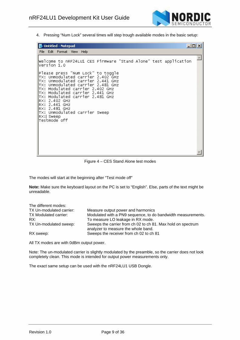
4. Pressing “Num Lock” several times will step trough available modes in the basic setup:
Figure 4 – CES Stand Alone test modes
The modes will start at the beginning after “Test mode off” Note: Make sure the keyboard layout on the PC is set to “English”. Else, parts of the text might be unreadable. The different modes: TX Un-modulated carrier: Measure output power and harmonics TX Modulated carrier: Modulated with a PN9 sequence, to do bandwidth measurements. RX: To measure LO leakage in RX mode. TX Un-modulated sweep: Sweeps the carrier from ch 02 to ch 81. Max hold on spectrum
analyzer to measure the whole band. RX sweep: Sweeps the receiver from ch 02 to ch 81 All TX modes are with 0dBm output power. Note: The un-modulated carrier is slightly modulated by the preamble, so the carrier does not look completely clean. This mode is intended for output power measurements only. The exact same setup can be used with the nRF24LU1 USB Dongle.

nRF24LU1 Development Kit User Guide
Revision 1.0 Page 10 of 36
4.1.2 Advanced setup Advanced setup gives access to all the different registers in the nRF24LU1 trough the CES PC-application. This setup is used during range test and other tests that require access to all parameters in the nRF24LU1. Advanced setup requires Microsoft .NET framework v2.0 runtime installed on the PC. It can be downloaded from Microsoft’s web pages. To use the CES PC application, follow these steps:
1. Install the nRF24LU1 CES software on the PC. 2. Connect the Basic Feature Board with the nRF24LU1 Radio Module in place, as
configured earlier, to a USB connector on the PC. 3. Start the nRF24LU1 CES application from the “Nordic Semiconductor” folder on the Start
menu. The following screen will appear:
Figure 5 – CES General Settings
The register settings in the bottom part of the screen reflect the settings done in the different tabs in the upper part. All parameters can be set using either the bottom register part, or by ticking the boxes in the upper part of the window. Please refer to the nRF24LU1 Product Specification for details. On the upper part of the window, two tabs can be selected, Configuration and Link Evaluation Configuration tab The “Update Device” button will transfer the settings to the nRF24LU1. The tab “general settings” has the following parameters, see Figure 5. Power up – sets the radio in standby mode
nRF24LU1 Development Kit User Guide
Revision 1.0 Page 11 of 36
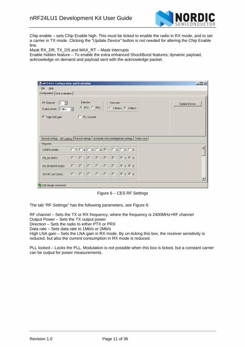
Chip enable – sets Chip Enable high. This must be ticked to enable the radio in RX mode, and to set a carrier in TX mode. Clicking the “Update Device” button is not needed for altering the Chip Enable line. Mask RX_DR, TX_DS and MAX_RT – Mask interrupts Enable hidden feature – To enable the extra enhanced ShockBurst features; dynamic payload, acknowledge on demand and payload sent with the acknowledge packet.
Figure 6 – CES RF Settings
The tab “RF Settings” has the following parameters, see Figure 6: RF channel – Sets the TX or RX frequency, where the frequency is 2400MHz+RF channel Output Power – Sets the TX output power Direction – Sets the radio to either PTX or PRX Data rate – Sets data rate to 1Mb/s or 2Mb/s High LNA gain – Sets the LNA gain in RX mode. By un-ticking this box, the receiver sensitivity is reduced, but also the current consumption in RX mode is reduced. PLL locked – Locks the PLL. Modulation is not possible when this box is ticked, but a constant carrier can be output for power measurements.

nRF24LU1 Development Kit User Guide
Revision 1.0 Page 12 of 36
Figure 7 – CES Packet settings
The tab “Packet settings” has the following parameters, see Figure 7 Data Pipe Enable – enable the data pipes by ticking the box. Address - sets the RX address of the different pipes. Payload width – sets the number of bytes in the payload from 0 to 32 bytes. TX address – sets the TX address. This must correspond with the RX address for the chosen pipe in the PRX device. To use the Auto Acknowledge function, the Data Pipe 0 and the TX address must be the same. CRC – can be set to 8 or 16 bits.
nRF24LU1 Development Kit User Guide
Revision 1.0 Page 13 of 36
Figure 8 – Auto acknowledge settings
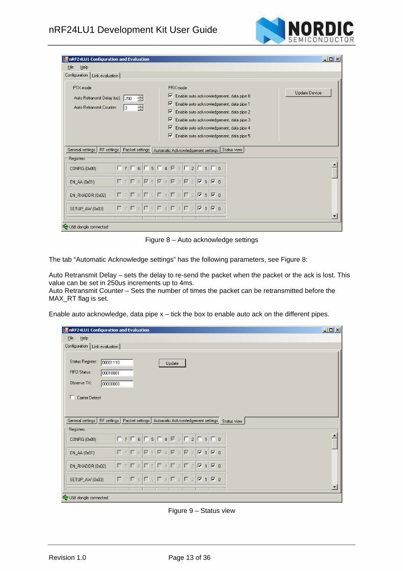
The tab “Automatic Acknowledge settings” has the following parameters, see Figure 8: Auto Retransmit Delay – sets the delay to re-send the packet when the packet or the ack is lost. This value can be set in 250us increments up to 4ms. Auto Retransmit Counter – Sets the number of times the packet can be retransmitted before the MAX_RT flag is set. Enable auto acknowledge, data pipe x – tick the box to enable auto ack on the different pipes.
Figure 9 – Status view
nRF24LU1 Development Kit User Guide
Revision 1.0 Page 14 of 36
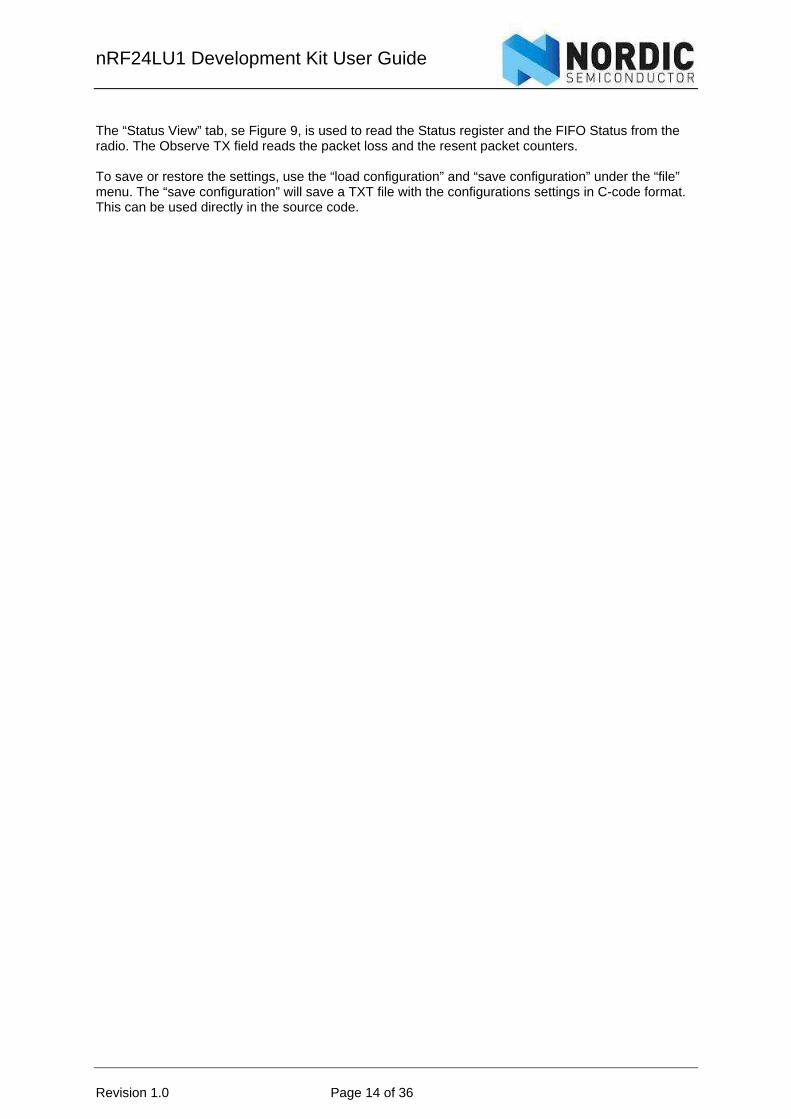
The “Status View” tab, se Figure 9, is used to read the Status register and the FIFO Status from the radio. The Observe TX field reads the packet loss and the resent packet counters. To save or restore the settings, use the “load configuration” and “save configuration” under the “file” menu. The “save configuration” will save a TXT file with the configurations settings in C-code format. This can be used directly in the source code.

nRF24LU1 Development Kit User Guide
Revision 1.0 Page 15 of 36
5 Output power measurements To measure the RF parameters, like output power and harmonics, you need a spectrum analyzer. Perform these steps to measure the output power of the carrier:
1. Connect a Basic Feature Board with a nRF24LU1 Radio Module SMA to a USB connector on the PC.
2. Connect a SMA coaxial cable from the SMA connector on the radio module to the spectrum analyzer.
3. Set the centre frequency to the nRF24LU1 operating frequency, span to 10MHz and level to +5dBm on the spectrum analyzer.
Use the CES in stand alone mode to enter the TX modes shown in Figure 4. Note: The carrier will be slightly modulated by the preamble so the carrier will not be a single tone. With a TX un-modulated carrier test running, the carrier should be visible on the spectrum analyzer.
nRF24LU1 Development Kit User Guide
Revision 1.0 Page 16 of 36
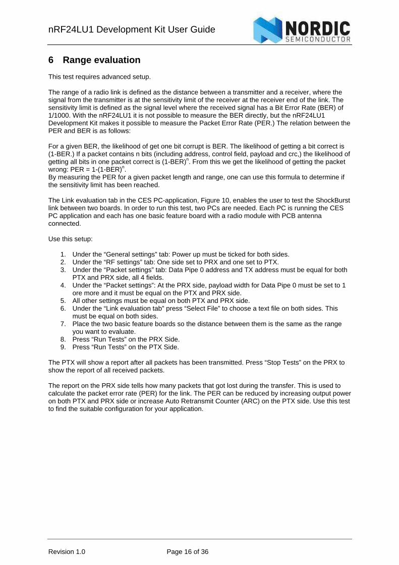
6 Range evaluation This test requires advanced setup. The range of a radio link is defined as the distance between a transmitter and a receiver, where the signal from the transmitter is at the sensitivity limit of the receiver at the receiver end of the link. The sensitivity limit is defined as the signal level where the received signal has a Bit Error Rate (BER) of 1/1000. With the nRF24LU1 it is not possible to measure the BER directly, but the nRF24LU1 Development Kit makes it possible to measure the Packet Error Rate (PER.) The relation between the PER and BER is as follows: For a given BER, the likelihood of get one bit corrupt is BER. The likelihood of getting a bit correct is (1-BER.) If a packet contains n bits (including address, control field, payload and crc,) the likelihood of getting all bits in one packet correct is (1-BER)n. From this we get the likelihood of getting the packet wrong: PER = 1-(1-BER)n. By measuring the PER for a given packet length and range, one can use this formula to determine if the sensitivity limit has been reached. The Link evaluation tab in the CES PC-application, Figure 10, enables the user to test the ShockBurst link between two boards. In order to run this test, two PCs are needed. Each PC is running the CES PC application and each has one basic feature board with a radio module with PCB antenna connected. Use this setup:
1. Under the “General settings” tab: Power up must be ticked for both sides. 2. Under the “RF settings” tab: One side set to PRX and one set to PTX. 3. Under the “Packet settings” tab: Data Pipe 0 address and TX address must be equal for both
PTX and PRX side, all 4 fields. 4. Under the “Packet settings”: At the PRX side, payload width for Data Pipe 0 must be set to 1
ore more and it must be equal on the PTX and PRX side. 5. All other settings must be equal on both PTX and PRX side. 6. Under the “Link evaluation tab” press “Select File” to choose a text file on both sides. This
must be equal on both sides. 7. Place the two basic feature boards so the distance between them is the same as the range
you want to evaluate. 8. Press “Run Tests” on the PRX Side. 9. Press “Run Tests” on the PTX Side.
The PTX will show a report after all packets has been transmitted. Press “Stop Tests” on the PRX to show the report of all received packets. The report on the PRX side tells how many packets that got lost during the transfer. This is used to calculate the packet error rate (PER) for the link. The PER can be reduced by increasing output power on both PTX and PRX side or increase Auto Retransmit Counter (ARC) on the PTX side. Use this test to find the suitable configuration for your application.

nRF24LU1 Development Kit User Guide
Revision 1.0 Page 17 of 36
Figure 10 - Link evaluation tab
Note: The test will only test the Enhanced ShockBurst link. For a real application, there will be a protocol layer on top that can handle lost packets on a more secure way. The Wireless Desktop Protocol (nRF2601) is an example of such a upper protocol layer.
nRF24LU1 Development Kit User Guide
Revision 1.0 Page 18 of 36
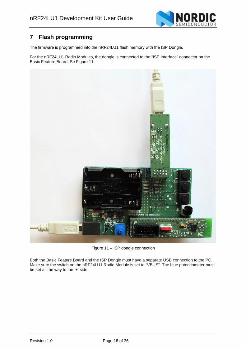
7 Flash programming The firmware is programmed into the nRF24LU1 flash memory with the ISP Dongle. For the nRF24LU1 Radio Modules, the dongle is connected to the “ISP Interface” connector on the Basic Feature Board. Se Figure 11.
Figure 11 – ISP dongle connection
Both the Basic Feature Board and the ISP Dongle must have a separate USB connection to the PC. Make sure the switch on the nRF24LU1 Radio Module is set to “VBUS”. The blue potentiometer must be set all the way to the ‘+’ side.
nRF24LU1 Development Kit User Guide
Revision 1.0 Page 19 of 36
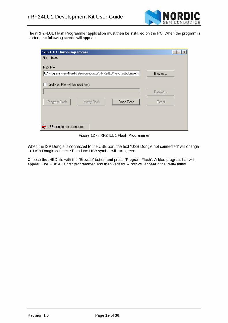
The nRF24LU1 Flash Programmer application must then be installed on the PC. When the program is started, the following screen will appear:
Figure 12 - nRF24LU1 Flash Programmer
When the ISP Dongle is connected to the USB port, the text “USB Dongle not connected” will change to “USB Dongle connected” and the USB symbol will turn green. Choose the .HEX file with the “Browse” button and press “Program Flash”. A blue progress bar will appear. The FLASH is first programmed and then verified. A box will appear if the verify failed.

nRF24LU1 Development Kit User Guide
Revision 1.0 Page 20 of 36
8 Wireless mouse demo This demo shows how the nRF24LU1 performs in a wireless mouse application. The demo is turning a wired PS/2 mouse into a wireless mouse running the wireless desktop protocol (nRF2601.) In this demo the nRF24LU1 is used in both ends of the link, while in a real wireless mouse application, the nRF24L01 would have been used in the mouse end. The following equipment is needed to run the test:
• 2 Basic feature boards with Radio Module with PCB antenna connected • 1 PS/2 adapter • 1 PS/2 mouse (not included in the Development kit.) • 1 PC running Windows XP (not included in the Development kit.) • 1 USB cable
Before the demo, the radio modules must be programmed with the right firmware. To access the needed files, please make sure the nRF24LU1 SDK is installed. The files can then be found at: C:\Program Files\Nordic Semiconductor\nRF24LU1\Source Code\Builds
After programming, all devices are unpaired and thus need to be paired. First time programming and pairing are committed using the following procedure:
Follow these steps to setup the development kit:
1. Select one of the Basic Feature Board with an nRF24LU1 Radio Module PCB to be used as the “Host side dongle” This will be connected to the PC via the USB cable during the demo.
2. Program the “Host side dongle” with the file usb_dongle.hex. Follow the instructions in the Flash programming chapter above
3. Unplug the “Host side dongle” from the PC.
4. Assemble an Basic Feature Board with a nRF24LU1 Radio Module PCB and one PS2 Adapter to work as the mouse module. The PS/2 adapter must be plugged into the “ISP Interface” connector after the flash is programmed.
5. Program the mouse module with the file mouse_keyboard.hex
6. Power down the mouse module and connect a PS2 mouse to the PS2 adapter. Plug the adapter into the “ISP Interface” connector on the Basic Feature Board.
7. Insert 3xAAA batteries into the battery holder on the Basic Feature Board.
8. Set the switch S1 on the radio module to VBAT.
9. Set the power switch on the Basic Feature Board to ON.
10. Connect the “Host side dongle” to the PC.
11. Start using the mouse within 5 seconds after insertion of the USB dongle.
12. The mouse module is now paired and ready for use.
Regarding the requirement of using the mouse within 5 seconds after insertion of the USB dongle, this is only required the very first time a mouse is to be paired. Once a pairing is successfully committed, all necessary pairing information is stored in Flash, thus pairing is not required on next power up. However, a previously paired mouse can easily be re-paired to another USB dongle by repeating procedure from 9 to 12. In this case, pairing to any previous dongle will be terminated.

nRF24LU1 Development Kit User Guide
Revision 1.0 Page 21 of 36
Figure 13: Basic Feature Board with PS/2 Adapter and nRF24LU1 Radio Module connected to a PS/2 Mouse
Instead of using a basic feature board with a Radio Module with PCB antenna as the “Host side dongle” one can use the nRF24LU1 USB dongle reference design. Please refer to the nRF24LU1 USB dongle User Guide for details on how to program it with the usb_dongle.hex file.

nRF24LU1 Development Kit User Guide
Revision 1.0 Page 22 of 36
9 In circuit software debugging It is possible to connect a FS2 System Navigator to the nRF24LU1 Radio Module to enable In circuit software debugging. The FS2 system navigator must be connected to the JTAG connector on the radio module. See Figure 14.
Figure 14: FS2 System Navigator connected to nRF24LU1 Radio Module
Refer to the document FS2 Installation.pfd under C:\Program Files\Nordic Semiconductor\nRF24LU1\Doc for instructions how to use and setup the FS2 system navigator. The FS2 system navigator is not included in the development kit and must be purchased separately from First Silicon Solutions. The FS2 System Navigator to be used with nRF24LU1 is the SNAV-CAST51. Note: The FS2 System Navigator and the ISP Dongle must never be connected to the system at the same time. Make sure that the FS2 Navigator is disconnected before the ISP Dongle is connected and vice versa.
No connection during FS2 Debugging!

nRF24LU1 Development Kit User Guide
Revision 1.0 Page 23 of 36
10 Using the Development Kit for prototyping The nRF24LU1 is designed to be used on the host side of the wireless link, connected to a host USB port. On the other end of the link, the nRF24L01 together with a MCU will be typical for most applications. However, using nRF24LU1 in both ends will give same link performance as if a nRF24LU1 was communicating with a nRF24L01. The nRF24LU1 Software Development Kit, SDK, is a good starting point to develop your own firmware. This comes with ready made libraries and example application, making it faster to get the application up and running. Please refer to the SDK documentation for details about the code and the use of this. The LEDs and buttons on the board can be used for debugging or in a real application if this is needed. The nRF24LU1 USB dongle is developed as a ready USB dongle. It has limited space for I/O connectors so it will be more convenient to use the Development Kit for prototyping and firmware development. The FS2 hardware debugger can only be connected to the Development Kit. Please refer to the nRF24LU1 USB dongle User Guide for details on how to use this in your development.

nRF24LU1 Development Kit User Guide
Revision 1.0 Page 24 of 36
11 Hardware description This chapter describes the hardware of the nRF24LU1 Development Kit.
11.1 Basic feature board The BFB contains power supply, connectors, battery holder, LEDs and buttons in order to supply the Development Kit with commonly used features. The Radio Module is inserted in the 40 pin dual in line socket on the BFB as shown in Figure 16. The nRF24LU1 radio module contains the nRF24LU1 and the necessary circuitry.
Figure 15 - Basic Feature Board
The nRF24LU1 Development Kit can be connected to a PC running the nRF24LU1 Configuration and Evaluation software to perform tests on the radio. A description of test setups with the nRF24LU1 Development Kit is described in the “nRF24LU1 Test Setup” document. Custom made firmware may also be run on the Development Kit. The schematic of the BFB is shown in Figure 17.

nRF24LU1 Development Kit User Guide
Revision 1.0 Page 25 of 36
Figure 16 - nRF24LU1 Development kit
11.2 Features of the BFB 11.2.1 Power supply The nRF24LU1 Development Kit BFB has two power supply options:
1. Through the USB cable 2. From the 3x AAA battery pack.
The switch close to the battery pack must be set to “ON” to enable supply from the battery. If the USB cable is connected, the power will be sourced from the USB even if the battery switch is set to “ON”. The nRF24LU1 Development Kit BFB has two power supply regulators; none of the regulators are used to supply the nRF24LU1 Radio Module. This is done by the internal regulator of the nRF24LU1. The nRF24LU1 radio module can be supplied with either USB power or from the battery pack by setting a switch on the Radio Module. The “ISP Interface” connector that is used for flash programming uses the adjustable regulator as a reference. For proper logic levels, the blue potentiometer must be set to max. 11.2.2 LED There are four yellow LEDs on the nRF24LU1 Development Kit BFB. Three of the LEDs are connected to the nRF24LU1 and can be used to indicate status, depending on the firmware that runs on the nRF24LU1. The green LED on the nRF24LU1 Development Kit BFB indicates the state of the battery switch. If it is lit, the battery switch is on and the batteries are ok.

nRF24LU1 Development Kit User Guide
Revision 1.0 Page 26 of 36
11.2.3 Buttons There are three buttons on the nRF24LU1 Development Kit BFB that are connected to the nRF24LU1. These are used to give input to the MCU during tests. The function of these buttons depends on the firmware on the nRF24LU1 11.2.4 Rotary Switch The rotary switch is not used when the BFB is used with the nRF24LU1 Radio Module. 11.2.5 SPI Interface This connector is used to program the FLASH on the nRF24LU1. The ISP dongle is then connected here. The pin out of this connector is shown in Table 1.
Pin Number Signal name Description 1 RF_VDD Supply voltage 2 Not used 3 RESET Reset signal to nRF24LU1 4 CSN SPI CSN 5 MISO SPI MISO 6 PROG PROG signal from nRF24LU1 7 MOSI SPI MOSI 8 SCK SPI SCK 9 Not used 10 GND Common ground
Table 1 - Pinout of the SPI Interface connector
11.2.6 Module connector A 40 pin dual in line socket, J1, is used to connect the nRF24LU1 Radio Module to the BFB. The pin out for this connector is given in Table 2.
Pin Number Signal name Description Connected to 1 GND Common ground 2 LED1 Led driver on Radio Module,
P0.0 LED 1
3 LED2 Led driver on Radio Module, P0.1
LED 2
4 LED3 Led driver on Radio Module, P0.2
LED 3
5 Not used LED 4 6 Not used 7 Not used 8 Not used 9 Not used 10 GND Common ground 11 Not used 12 P0.5 GPIO P0.5 Button B1 13 P0.4 GPIO P0.4 Button B2 14 P0.3/CSN GPIO P0.3 or SPI CSN Button B3 15 Not used 16 Not used 17 Not used

nRF24LU1 Development Kit User Guide
Revision 1.0 Page 27 of 36
Pin Number Signal name Description Connected to 18 Not used 19 GND Common ground 20 Not used 21 Not used 22 Not used 23 Not used 24 Not used 25 Not used 26 GND Common ground 27 VBUS USB supply voltage input USB Connector 28 VDD Regulated voltage input Output of fixed reg. 29 GND Common ground 30 D- USB D- signal USB Connector 31 D+ USB D+ signal USB Connector 32 GND Common ground 33 P0.0/SCK GPIO P0.0 or SPI SCK SPI INTERFACE 34 P0.2/MISO GPIO P0.2 or SPI MISO SPI INTERFACE 35 P0.1/MOSI GPIO P0.1 or SPI MOSI SPI INTERFACE 36 P0.3/CSN SPI CSN SPI INTERFACE 37 RESET nRF24LU1 Reset SPI INTERFACE 38 PROG nRF24LU1 Prog SPI INTERFACE 39 Not used 40 VBAT Battery Voltage Battery pack
Table 2 - Module connector J1 pin out
11.2.7 Signal grid The signal grid is a grid of 5 x 6 trough-hole pads. All signals that is present on the BFB are routed trough this grid. The pin out is shown in Table 3. Pin Number Signal name Description Connected to 1 VBAT Battery Switch 2 VDD_REG_RF Output of variable reg. 3 PROG nRF24LU1 Prog 4 RESET nRF24LU1 Reset 5 CSN SPI CSN 6 P0.1 GPIO LED 2 7 P0.0 GPIO LED 1 8 SCK SPI SCK 9 MISO SPI MISO 10 MOSI SPI MOSI 11 P0.2 GPIO LED 3 12 Led 4 Not connected to the nRF24LU1 LED 4 13 J1 pin 8 Not used 14 J1 pin 7 Not used 15 J1 pin 6 Not used 16 P0.5 GPIO Button B3 17 P0.4 GPIO Button B2 18 P0.3 GPIO Button B1 19 J1 pin 11 Not used 20 J1 pin 9 Not used 21 SPARE 6 Not used 22 J1 pin 18 Not used Rotary switch 23 J1 pin 17 Not used Rotary switch

nRF24LU1 Development Kit User Guide
Revision 1.0 Page 28 of 36
Pin Number Signal name Description Connected to 24 J1 pin 16 Not used Rotary switch 25 J1 pin 15 Not used Rotary switch 26 SPARE 5 Not used 27 SPARE 4 Not used 28 SPARE 3 Not used 29 SPARE 2 Not used 30 SPARE 1 Not used
Table 3 - Pin out of the signal grid
123456789
10111213141516171819202122232425262728293031323334353637383940
J1
40PIN
VDDVBUSGND
D-D+GNDSCKMISOMOSICSNCEIRQ
P0.7
GND
P1.0P1.1P1.2P1.3P1.4P1.5P1.6P0.6
GND
P2.0P2.1P2.2P2.3
GND
GND
VBUS
VDD
D-D+
VDD_REG_RFP0.7P1.0P1.1P1.2P1.3P1.4P1.5P1.6
VDD_REG_RF
P2.4
P2.5
P2.6
P2.7
GND
P1.
0
P2.
1
P2.
2
P2.7
P2.7P2.6P2.5P2.4
RF_VDD
IRQMISO
CECSN
MOSISCK
12345678
J2
nRF24L01
1234
J3
USB_B
VBUS
CECSN
SCKMOSI
MISOIRQ
RF_VDD
123456789
10
J4
HEADER 10
P0.5P0.4P0.3P0.2P0.1P0.0
C310nF
OUT1
ADJ2
GN
D3
BYP4
SHDN5
GN
D6
GN
D7
IN8
U1LT1763CS8
+ C410uF/6V
1 2S1
Battery
+C12.2uF/20V C5
100nF/16V
RF_VDD
R110K0603
C2100nF/50V0805
(VDD_nRF = 1.8V - 3.6V)
1 2
JP101JUMPER
13
2
64
5
R60-10K
R34.7K0603
R47.5K0603
R522K0603
R25.6K
Supply Level Adjust, 1.9V - 3.6V
xxx
xxx
xxx
xxx
12
JB_1
CON2
D1
BAT-54
VDD
+ C810uF3216
C61uF/20V3216
OUT1
SENSE2
GN
D3
BYP4
SH DN5
GN
D6
GN
D7
IN8
U2LT1763CS8-3
C710nF
Un-regulated
D2
BAT-54
VBUS
SPARE_1SPARE_2SPARE_3SPARE_4SPARE_5SPARE_6
LED5Green
LED1LED
LED2LED
LED3LED
LED4LED
R10150ohm
R11150ohm
R12150ohm
R13150ohm
R14150ohm
VDD
S2SW1
B1
R1510K
S3SW1
B2
R1610K
S4SW1
B3
R1710K
P0.7
1 8C C4 2
SW1
CODE SWITCH PT65
P2.
3
P1.
1
P1.
2
P1.
3
+ C910uF/6V
P0.6
VDD_REG_RF
Figure 17 - Schematic of the nRF24LU1 Development Kit Basic Feature Board
11.3 PS/2 Adapter The nRF24LU1 Development kit contains one PS/2 Adapter. These are simple level shifters and a DC-DC cconverter that enables a PS/2 Mouse or Keyboard to be connected to the nRF24LU1. The PS/2 Adapter connects to the “ISP Interface” connector on the BFB. This setup is intended to emulate a wireless mouse or keyboard using existing devices. The schematic and layout for the PS/2 Adapter is shown in Figure 18 and Figure 19. The BOM is in Table 5. The PS/2 is a bi-directional synchronous link, with one data line and one clock line. The power supply and the logic levels are 5v TTL. To interface this to the nRF24LU1, the PS/2 adapter is used. The DC-DC converter is a MAX619 3v to 5v IC.
nRF24LU1 Development Kit User Guide
Revision 1.0 Page 29 of 36
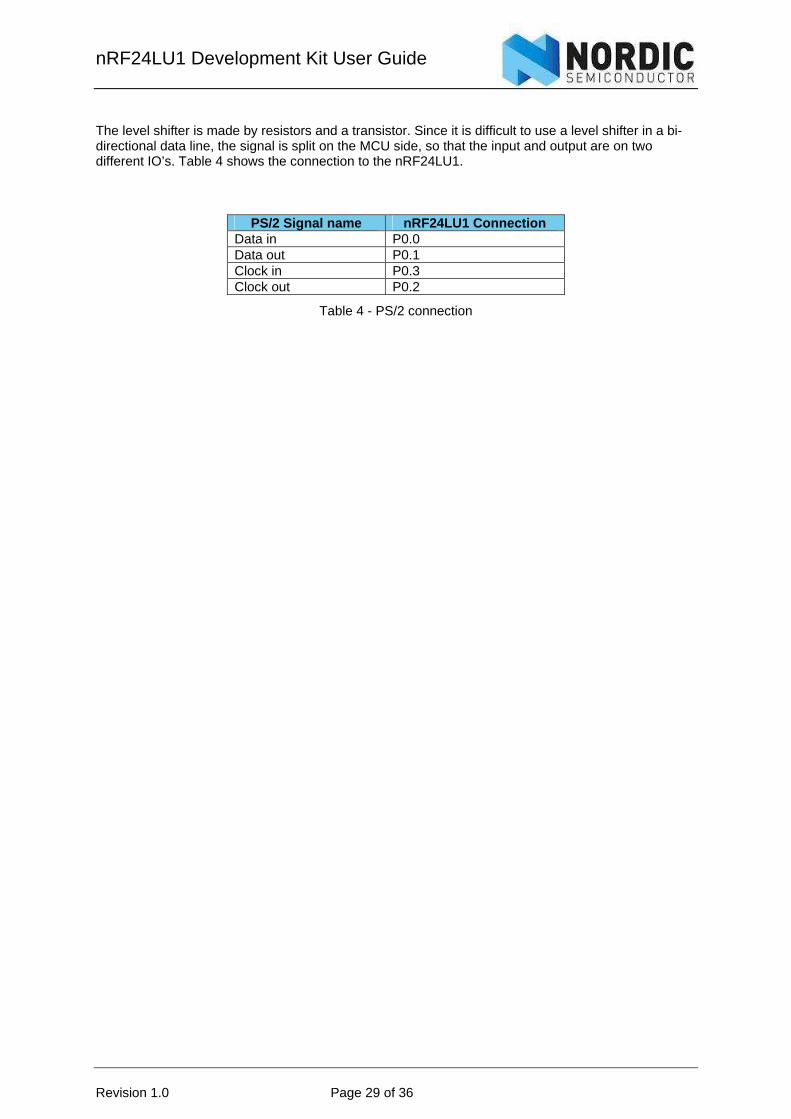
The level shifter is made by resistors and a transistor. Since it is difficult to use a level shifter in a bi-directional data line, the signal is split on the MCU side, so that the input and output are on two different IO’s. Table 4 shows the connection to the nRF24LU1.
PS/2 Signal name nRF24LU1 Connection Data in P0.0 Data out P0.1 Clock in P0.3 Clock out P0.2
Table 4 - PS/2 connection

nRF24LU1 Development Kit User Guide
Revision 1.0 Page 30 of 36
xxx
123456
J1
PS2VDD
Clock
Data
BC847C
T2
BC847C
T1
1kR4
1kR5
1kR8
1kR9
10k
R6
10k
R7
C1+1
IN2
OUT3
C2+4
C2-5GND 6
SHDN 7C1- 8
MAX619CSA
U3
10uF
C20
10uF
C21
1uF
C23
1uF
C22
VDD PS2VDD
1kR17
1kR18
2k2R19
2k2R20
1 23 45 67 89 10
IDC 10 female
J2VDD
GND
Figure 18 - Schematics of the PS/2 Adapter
Designator Value Footprint Comment
C20, C21 10uF 3216 10uF Tantal 10V
C22, C23 1uF 3216[1206] 1uF X5R, +/-10% 6.3V
J1 MiniDIN 6-pin MiniDIN
J2 IDC 10 female HDR2x5 R4, R5, R8, R9, R17, R18 1k 0603s 5% R6, R7 10k 0603s 5% R19, R20 2k2 0603s 5% T1, T2 BC847C SOT-23 BC847C U3 MAX619CSA SO8 MAX619 PCB 0007KJO
Table 5 - PS/2 Adapter BOM
nRF24LU1 Development Kit User Guide
Revision 1.0 Page 31 of 36
Top silkscreen
No components in bottom layer
Top signal layer
Bottom signal layer
Figure 19 - PS/2 Adapter layout
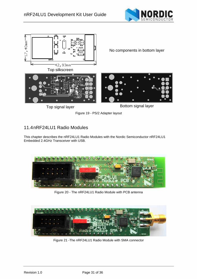
11.4 nRF24LU1 Radio Modules This chapter describes the nRF24LU1 Radio Modules with the Nordic Semiconductor nRF24LU1 Embedded 2.4GHz Transceiver with USB.
Figure 20 - The nRF24LU1 Radio Module with PCB antenna
Figure 21 -The nRF24LU1 Radio Module with SMA connector

nRF24LU1 Development Kit User Guide
Revision 1.0 Page 32 of 36
The Radio Modules for the nRF24LU1 Embedded 2.4GHz Transceiver with USB has been developed to enable customers to test functionality, run communication and verify the performance parameters of the device. The nRF24LU1 Radio Modules comes with the nRF24LU1 DEVKIT .The modules come in two versions; one with a SMA connector and one with a quarter wave PCB antenna. The module with SMA connector is developed to make it easy to do conducted measurements to test the performance of the radio. Except for the antenna, the modules have the same layout and same Bill of Material. The nRF24LU1 Radio Modules are intended for evaluation and development purposes only.
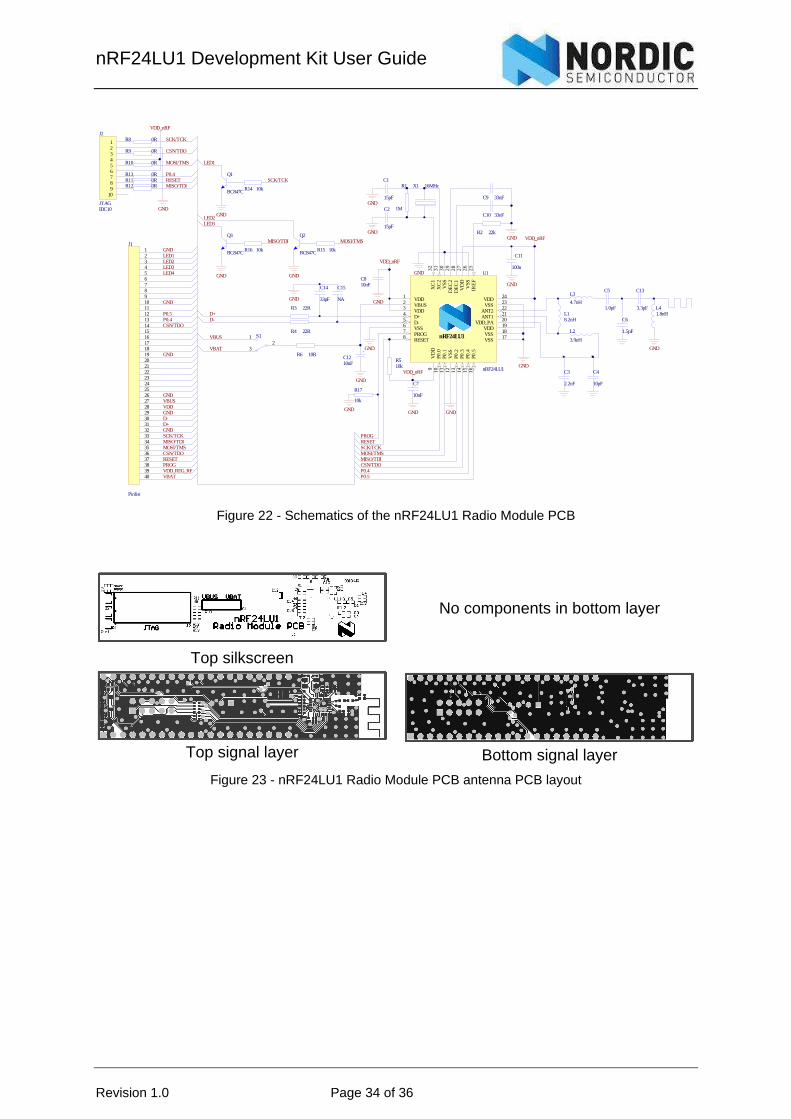
11.5 nRF24LU1 Radio Module hardware description Figure 22 to Figure 25 shows the nRF24LU1 Radio Modules circuit diagrams and PCB layouts. The BOM is given in Table 8. The module has the nRF24LU1 and all necessary circuit to start using the nRF24LU1. It plugs into the 40 pin DIL connector of the Basic Feature Board (BFB). All I/Os are then available on the Basic Feature Board. 11.5.1 Debugger interface To use the built in debugger of the nRF24LU1, a JTAG/FS2 interface, J2, is available on the module.
J2 pin JTAG/FS4 name 1 TCK 2 GND 3 TDO 4 VDD 5 TMS 6 VDD 7 Trig out / P0.4 8 RESET 9 TDI 10 Not used
Table 6 - FS2 Debug Interface
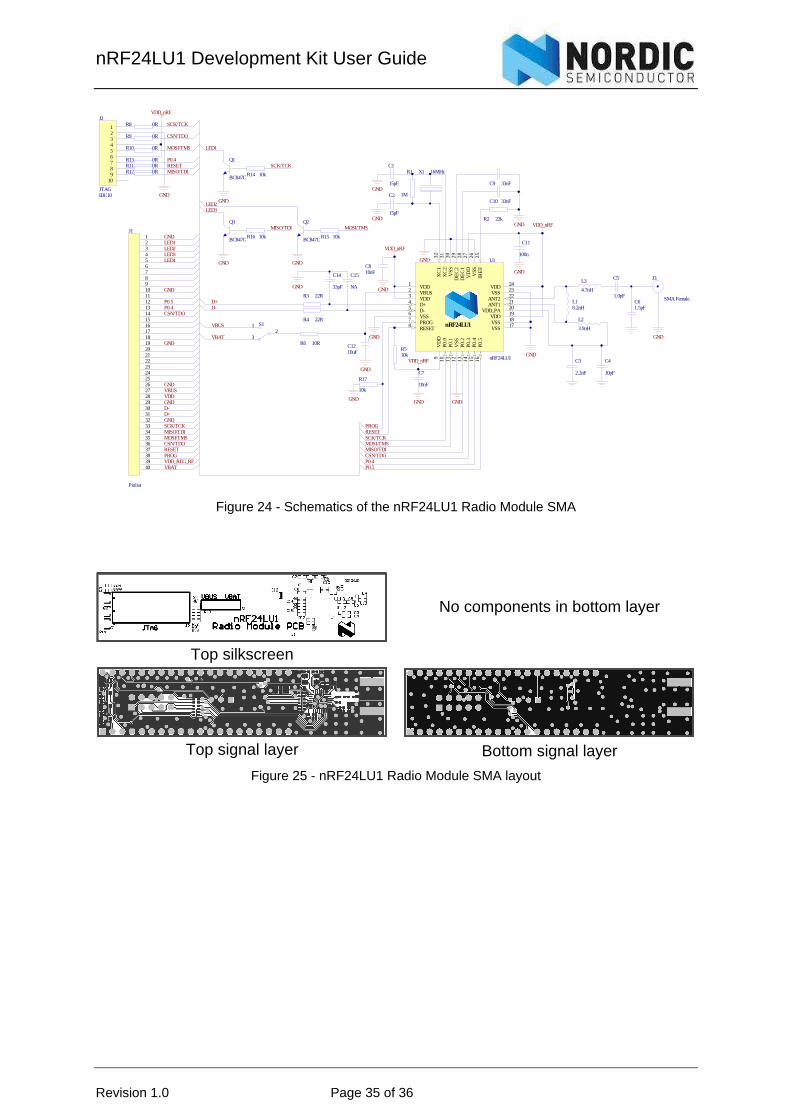
11.5.2 Led drivers LED 1-3 on the BFB is driven with LED drivers on the Radio Module 11.5.3 Power Supply Switch The switch S1 can be used to switch the power supply between the battery pack on the BFB for stand alone use, or to VBUS from the USB connector. 11.5.4 Flash programming The FLASH in the nRF24LU1 can be programmed from the “ISP Interface” connector on the BFB by using the ISP Dongle Note: The JTAG connector on the Radio Modules is not pin compatible with the ISP Dongle from Nordic Semiconductor and can not be used to program the flash. 11.5.5 Antenna For connection of a single ended antenna or to any 50Ω test equipment, the nRF24LU1 Radio Module with the SMA connector can be used.

nRF24LU1 Development Kit User Guide
Revision 1.0 Page 33 of 36
The nRF24LU1 Radio Module PCB has an integrated PCB antenna for general testing. Except from the PCB antenna and the SMA connector, the modules are identical. C14 on the nRF24LU1 Radio Module PCB is to match the antenna to the 50 ohm antenna interface and is not present on the SMA version of the module. 11.5.6 40 pin DIL connector
Pin number Description 1 GND 2 LED1 3 LED2 4 LED3 5 LED4 – Not used 6 Not used 7 Not used 8 Not used 9 Not used 10 GND 11 Not used 12 P0.5 13 P0.4 14 P0.3 15 Not used 16 Not used 17 Not used 18 Not used 19 GND 20 Not used 21 Not used 22 Not used 23 Not used 24 Not used 25 Not used 26 GND 27 VBUS 28 VDD – Not used 29 GND 30 D+ 31 D- 32 GND 33 P0.0 / SCK 34 P0.2 / MISO 35 P0.1 / MOSI 36 P0.3 / CSN 37 RESET 38 PROG 39 VDD Adjustable – Not used 40 VBAT
Table 7 - Pin out of the module connector
The nRF24LU1 Radio Module is manufactured on a 1.6mm thick, 2 layer FR4 substrate.
nRF24LU1 Development Kit User Guide
Revision 1.0 Page 34 of 36
12345678910111213141516171819202122232425262728293031323334353637383940
Pinlist
J1
VDDVBUSGND
D-D+GNDSCK/TCK
MOSI/TMSMISO/TDI
CSN/TDO
PROGVDD_REG_RF
GND
LED2LED3LED4
GND
P0.4CSN/TDO
GND
GND
VBUS
D-D+
P0.4P0.5
SCK/TCKMOSI/TMSMISO/TDICSN/TDO
PROG
10RR6
8.2nHL1
2.2nF
C3
10pF
C4
4.7nH
L3
3.9nH
L2
1.0pF
C5
1.5pF
C6
15pF
C2
15pF
C1
1M
R1 16MHzX1
VDD_nRF
VDD_nRF
22kR2
GND
GND
10nF
C7
33nFC10
10nFC8
GND
100n
C11
VDD_nRF
22RR3
22RR4
GND10kR5
GND
GND
GND
GND
33nFC9
GND
GND
10uFC12
GND
RESET
JTAG
SCK/TCK
RESET
123456789
10
IDC10
J2
CSN/TDO
MOSI/TMS
MISO/TDI
GND
VDD_nRF
P0.5
VBAT
23
1 S1
VBAT
RESET
0RR8
0RR9
0RR10
0RR110RR12
nRF24LU1
P0.5
16
VSS 23
ANT121
VDD_PA20
XC
132
VDD1
RESET8PROG7
D+4
D-5
VSS6
VBUS2
VSS 18
DE
C2
29
VDD3
VSS
12
XC
231
VDD 24
VD
D9
ANT222
VSS 17
VDD 19
IRE
F25
DE
C1
28
nRF24LU1
P0.0
10
P0.1
11
VD
D27
VSS
30
P0.2
13
P0.3
14
P0.4
15V
SS26
U1
P0.40RR13
LED110kR16
Q3
BC847C 10kR15
Q2
BC847C
10kR14
Q1
BC847C
GND
GND
LED1
LED2LED3
SCK/TCK
MISO/TDI MOSI/TMS
GND
10k
R17
GND
3.3pF
C13
1.8nHL4
GND
33pF
C14
NA
C15
GND
Figure 22 - Schematics of the nRF24LU1 Radio Module PCB
Top silkscreen
No components in bottom layer
Top signal layer
Bottom signal layer
Figure 23 - nRF24LU1 Radio Module PCB antenna PCB layout
nRF24LU1 Development Kit User Guide
Revision 1.0 Page 35 of 36
12345678910111213141516171819202122232425262728293031323334353637383940
Pinlist
J1
VDDVBUSGND
D-D+GNDSCK/TCK
MOSI/TMSMISO/TDI
CSN/TDO
PROGVDD_REG_RF
GND
LED2LED3LED4
GND
P0.4CSN/TDO
GND
GND
VBUS
D-D+
P0.4P0.5
SCK/TCKMOSI/TMSMISO/TDICSN/TDO
PROG
10RR6
8.2nHL1
2.2nF
C3
10pF
C4
4.7nH
L3
3.9nH
L2
1.0pF
C5
1.5pFC6
15pF
C2
15pF
C1
1M
R1 16MHzX1
VDD_nRF
VDD_nRF
22kR2
GND
GND
10nF
C7
33nFC10
10nFC8
GND
100n
C11
VDD_nRF
22RR3
22RR4
GND10kR5
GND
GND
GND
GND
33nFC9
GND
GND
10uFC12
GND
RESET
JTAG
SCK/TCK
RESET
123456789
10
IDC10
J2
CSN/TDO
MOSI/TMS
MISO/TDI
GND
VDD_nRF
P0.5
VBAT
23
1 S1
VBAT
RESET
0RR8
0RR9
0RR10
0RR110RR12
nRF24LU1
P0.5
16
VSS 23
ANT1 21
VDD_PA 20
XC
132
VDD1
RESET8 PROG7
D+4
D-5
VSS6
VBUS2
VSS 18
DE
C2
29
VDD3
VSS
12
XC
231
VDD 24
VD
D9
ANT2 22
VSS 17
VDD 19
IRE
F25
DE
C1
28
nRF24LU1
P0.0
10
P0.1
11
VD
D27
VSS
30
P0.2
13
P0.3
14
P0.4
15V
SS26
U1
P0.40RR13
LED110kR16
Q3
BC847C 10kR15
Q2
BC847C
10kR14
Q1
BC847C
GND
GND
LED1
LED2LED3
SCK/TCK
MISO/TDI MOSI/TMS
GND
10k
R17
GND
J3
SMA Female
GND
33pF
C14
NA
C15
GND
Figure 24 - Schematics of the nRF24LU1 Radio Module SMA
Top silkscreen
No components in bottom layer
Top signal layer
Bottom signal layer
Figure 25 - nRF24LU1 Radio Module SMA layout

nRF24LU1 Development Kit User Guide
Revision 1.0 Page 36 of 36
Designator Value Comment C1, C2 15pF NPO, +/-2% 50V C3 2.2nF X7R, +/-10% 50V C4, C13 4.7pF NP0 +/-0.25pF, 50V C5 1.5pF NP0 +/-0.1pF, 50V C6 1.0pF NP0 +/-0.1pF, 50V C7, C8 10nF X7R, +/-10% 50V C9, C10 33nF X7R, +/-10% 50V C11 100n X7R, +/-10% 50V
C12 10uF Tantal 10V
C13 4.7pF NP0 +/-0.25pF, 50V. Only on PCB antenna version
C14 33pF NPO, +/-2% 50V C15 NA
J1 Pinlist
J2 IDC10 Header 2x5 pin J3 SMA Female Only on SMA version L1 8.2nH Chip inductor +/-5%. Murata LQP15-series L2 2.7nH Chip Inductor +/-5%. Murata LQP15-series L3 3.9nH Chip inductor +/-5%. Murata LQP15-series Q1, Q2, Q3 BC847C BC847C R1 1M 5% R2 22k 1% R3, R4 22R 5% R5, R14, R15, R16, R17 10k 5% R6 10R 5% R8, R9, R10, R11, R12, R13 0R S1 Switch
U1 nRF24LU1 nRF24LU1
X1 16MHz TSX-4025, CL=9pF, +/-10%. Se product specification for details.
PCB 0008KJO nRF24LU1 Radio Module SMA PCB 0009KJO nRF24LU1 Radio Module PCB
Table 8 - nRF24LU1 Radio Module Bill of material, common to both versions, except where noted


