All rights reserved. Reproduction in whole or in part is prohibited without the prior written permission of the copyright holder. 2010-11-03 nRF24Z1 2.4 GHz wireless audio streamer Product Specification v1.0 Key Features • Low cost 0.18 μ CMOS process, 36 pin 6×6 mm QFN package • Single chip 2.4 GHz RF transceiver • 4 Mbit/sec RF link • Input/output sample rate up to 48kSPS, 24 bit • Programmable latency • Quality of Service engine supporting up to 1.536 Mbit/s LPCM audio • S/PDIF interface for direct connection to computer soundcard and surround receivers • I2S interface for glue-less audio support • SPI or 2-wire interface for up to 12 kbit/s peak bi-directional digital control/AUX data • On-chip optional compression • On-chip voltage regulators • Few external components • Uses global 2.4 GHz band Applications • CD quality headsets • Headsets • Speakers • Surround speakers • Microphone • Audio streaming from computer soundcard to HiFi system
Transcript
All rights reserved.Reproduction in whole or in part is prohibited without the prior written permission of the copyright holder.
• Single chip 2.4 GHz RF transceiver• 4 Mbit/sec RF link• Input/output sample rate up to 48kSPS, 24
bit• Programmable latency• Quality of Service engine supporting up to
1.536 Mbit/s LPCM audio• S/PDIF interface for direct connection to
computer soundcard and surround receivers
• I2S interface for glue-less audio support• SPI or 2-wire interface for up to 12 kbit/s
peak bi-directional digital control/AUX data• On-chip optional compression• On-chip voltage regulators• Few external components• Uses global 2.4 GHz band
Applications
• CD quality headsets• Headsets• Speakers• Surround speakers• Microphone• Audio streaming from computer soundcard to
HiFi system
Page 2 of 85
nRF24Z1 Product Specification
Revision 1.0
Liability disclaimer
Nordic Semiconductor ASA reserves the right to make changes without further notice to the product to improve reliability, function or design. Nordic Semiconductor ASA does not assume any liability arising out of the application or use of any product or circuits described herein.
Life support applications
These products are not designed for use in life support appliances, devices, or systems where malfunction of these products can reasonably be expected to result in personal injury. Nordic Semiconductor ASA customers using or selling these products for use in such applications do so at their own risk and agree to fully indemnify Nordic Semiconductor ASA for any damages resulting from such improper use or sale.
Contact details
For your nearest dealer, please see www.nordicsemi.com
Nordic Semiconductor’s products meet the requirements of Directive 2002/95/EC of the European Parliament and of the Council on the Restriction of Hazardous Substances (RoHS). Complete hazardous substance reports as well as material composition reports for all active Nordic products can be found on our web site www.nordicsemi.com.
Revision History
Date Version DescriptionNovember 2010 1.0 Product specification
1 Introduction .................................................................................................51.1 Quick reference data ............................................................................51.2 Prerequisites.........................................................................................51.3 Writing conventions ..............................................................................52 Product overview ........................................................................................62.1 Pin assignments ...................................................................................62.2 Pin functions ........................................................................................73 Architectural overview................................................................................93.1 Fundamental modes of operation .........................................................103.2 Communication and data transfer principle ..........................................103.3 Mode- and Interface alternatives ..........................................................133.4 Audio transmitter (ATX) ........................................................................143.5 Audio Receiver (ARX)...........................................................................173.6 Blocks and functionality common to the ATX abd ARX ........................204 Operation overview .....................................................................................224.1 Power on/RESET sequence .................................................................224.2 RF link initialization ...............................................................................224.3 Audio channel .......................................................................................234.4 Control channel.....................................................................................244.5 Power down mode ................................................................................255 nRF24Z1 register MAP ................................................................................265.1 Register access from the ATX side ......................................................265.2 Register access from the ARX side ......................................................265.3 Register map in external EEPROM ......................................................296 Digital I/O......................................................................................................306.1 Digital I/O behavior during RESET .......................................................306.2 Audio interfaces ....................................................................................306.3 Serial master interfaces ........................................................................386.4 Control and GPIO interfaces.................................................................436.5 Data exchange between an ATX and ARX...........................................517 Quality of Service (QoS) and RF-protocol ................................................537.1 Link establishment ................................................................................537.2 RF protocol ...........................................................................................537.3 Adaptive Frequency Hopping (AFH).....................................................547.4 Link registers ........................................................................................577.5 RF output power ...................................................................................598 Interrupts......................................................................................................609 RESET outputs ............................................................................................6210 Power down control ....................................................................................6310.1 Activation of power down mode............................................................6310.2 Wake up from power down ...................................................................6310.3 nRF24Z1 power saving example ..........................................................6611 Register update over the control channel ................................................6711.1 Register update and device relink ........................................................68
Page 3 of 85Revision 1.0
nRF24Z1 Product Specification
12 Test mode ....................................................................................................7013 Electrical specifications .............................................................................7114 Absolute maximum ratings ........................................................................7515 Mechanical specifications ..........................................................................7616 Ordering information ..................................................................................7716.1 Package marking ..................................................................................7716.2 Abbreviations ........................................................................................7717 Application information ..............................................................................7817.1 Antenna I/O...........................................................................................7817.2 Crystal specification..............................................................................7817.3 Bias reference resistor..........................................................................7817.4 Internal digital supply de-coupling ........................................................7817.5 PCB layout and de-coupling guidelines ................................................7818 Reference circuits .......................................................................................8018.1 nRF24Z1 schematics............................................................................8018.2 nRF24Z1 layout ....................................................................................8218.3 ARX BoM ..............................................................................................8419 Glossary .......................................................................................................85
Page 4 of 85Revision 1.0
nRF24Z1 Product Specification
1 Introduction
nRF24Z1 provides a true single chip system for CD quality audio streaming of up to16 bit 48 kSPS audio, supporting up to 24 bit 48 kSPS input. I2S and S/PDIF interfaces are supported for audio input/output (I/O). Seamless interfacing of low cost A/D and D/A for analog audio input and output. SPI or 2-wire (I2C compatible) control serial interfaces. Embedded voltage regulators yield maximum noise immunity and allow operation from a single 2.0V to 3.6V supply.
1.1 Quick reference data
Table 1.nRF24Z1 quick reference data
1.2 Prerequisites
In order to fully understand this product specification, a good knowledge of electronic and software engineering is necessary.
1.3 Writing conventions
This product specification follows a set of typographic rules to make the document consistent and easy to read. The following writing conventions are used:
• Commands, bit state conditions, and register names are written in Courier New.• Pin names and pin signal conditions are written in Courier New bold.• Cross references are underlined and highlighted in blue.
Parameter Value UnitMinimum supply voltage 2.0 VTemperature range -20 to +80 °CPeak supply current in transmit @ -5dBm output power
15 mA
Peak supply current in receive mode
32 mA
Supply current in power down mode 5 µAMaximum transmit output power 0 dBmAudio sample rate 8 to 48 kSPSAudio resolution 16 bitReceiver sensitivity -80 dBm
Page 5 of 85Revision 1.0
nRF24Z1 Product Specification
2 Product overview
2.1 Pin assignments
Figure 1. Pin assignments
nRF24Z1QFN36 6x6
32
VDD
VSS
IREF
1817161510 11 12 13 14
19
20
21
22
27
26
25
24
23
9
8
7
6
1
2
3
4
5
2829303136 35 34 33
VSS
VDD
VSS_PA
ANT2
ANT1
XC1
XC2
VSS
DVD
D
VSS
WS
DA
TA
CLK
IRQ
/D
O[3]/
PWM
DD[0]/DI[0]
DD[1]/DI[1]
SMOSI/DD[2]/DI[2]
SCSN/SADR/DI[3]
SSCK/SSCL/DO[0]
SMISO/SSDA/DO[1]
MM
OSI
MC
SN
MM
ISO
VDD
SSEL/DO[2]
VDD_PA
MSDA
MSC
L
SPDIO
MC
LK
MSC
K
REQ
MODE
Page 6 of 85Revision 1.0
nRF24Z1 Product Specification
P
2.2 Pin functions
Table 2. shows the nRF24Z1 pin functions. Note that pin functions depend on the functional mode of the device (ATX; audio source or ARX; audio recipient) and the interface of choice.
in number Pin name Pin function Description
Serial slave interface
ARX GPIO Serial slave interface
ARX GPIOinterface
ATX/ARX w. serial slave
interface
ARX w. GPIO interface
1 SSEL DO[2] Digital Input Digital Output Slave interface select 1:2-wire,
0:SPI
GPIO out bit #2
2 SMISO/SSDA DO[1] Digital Output/ Digital IO
Slave SPI serial out
/ Slave 2-wire data (bidir)
GPIO out bit #1
3 SSCK/SSCL DO[0] Digital Input Digital Output Slave SPI clock/ Slave 2-wire
clock
GPIO out bit #0
4 SCSN/SADR DI[3] Digital Input Slave SPI slave select/ Address
select 2-wire slave
GPIO in bit #2
5 VDD Power Power Supply (2.0-3.6 V DC)6 SMOSI/DD[2] DI[2] Digital Input Slave SPI
serial in/ Direct data in
bit #2
GPIO in bit #3
7 DD[1] DI[1] Digital Input Direct data in bit #1
GPIO in bit #1
8 DD[0] DI[0] Digital Input Direct data in bit #0
GPIO in bit #0
ATX ARX9 REQ Dig. Out Dig. In For ATX not connected, for ARX
connect to VSS10 CLK Dig. IO Dig. Out I2S bit clock11 WS Dig. IO Dig. Out I2S word clock12 DATA Dig. In Dig. Out I2S word clock13 SPDIO Dig. In Dig. Out S/PDIF interface14 MCLK Digital Output 256X sample rate clock to ADC
or DAC15 DVDD Regulator output Digital voltage regulator output
for decoupling16 VSS Power Ground (0V)17 XC2 Analog output Crystal Pin 218 XC1 Analog input Crystal Pin 119 VDD Power Power Supply (2.0-3.6 V DC)20 VDD_PA Regulator output DC output (+1.8V) for RF
30 MMISO Digital Input Master SPI serial input31 MMOSI Digital Output Master SPI serial output32 VSS Power Ground (0V)33 VDD Power Power Supply (2.0-3.6 V DC)34 VSS Power Ground (0V)35 MSCK Digital Output Master SPI clock36 IRQ DO[3]/PWM Digital Output Interrupt
requestGPIO out bit #3/ PWM output
in number Pin name Pin function Description
Page 8 of 85Revision 1.0
nRF24Z1 Product Specification
3 Architectural overview
nRF24Z1 is a 4 Mbit/s single chip RF transceiver that operates in the world wide 2.4 GHz license free ISM band. The nR24Z1 is based on the proven nRF24xx radio- and ShockBurst™ platforms from Nordic Semiconductor.
The device offers a wireless channel for seamless streaming of LPCM or compressed audio in parallel with a low data rate control channel. To enable this, the device offers the following features in addition to the nRF24xx RF platform:
• Standard digital audio interfaces (I2S, S/PDIF)• Fully embedded Quality of Service engine handling all RF protocol and RF link tasks. • SPI and 2-wire master and slave control interfaces• GPIO pins
As all processing related to audio I/O, RF protocol and RF link management is embedded, the nRF24Z1 offers a transparent audio channel with capacity of up to 1.54 Mbit/s, with no true time processing needed. The nRF24Z1 can be utilized in systems without external microcontroller or used in conjunction with a simple microcontroller that only need to handle low speed tasks over the serial or parallel ports (for example, volume up/down).
A block schematic of a typical nRF24Z1 based system is illustrated in Figure 2.
Figure 2. Typical audio application using nRF24Z1
In this system a DSP or microcontroller feeds data from a storage device to an nRF24Z1 using standard audio format (I2S). An nRF24Z1 pair transfers audio data from the source and presents it to a stereo DAC on the receiving side. From the application side, the nRF24Z1 link will appear as an open channel (like a cable).
Initial configuration of nRF24Z1 is done by the microcontroller through an SPI or 2-wire control interface.
Storage DSP / Microcontroller nRF24Z1 nRF24Z1
DAC and audio
amplifier
Microcontroller
I2SSPI
I2S
Audio Source Destination
Audiotransmitter
Audioreceiver
MCLKSPI
Page 9 of 85Revision 1.0
nRF24Z1 Product Specification
3.1 Fundamental modes of operation
A wireless system streaming audio will have an asymmetrical load on the RF link as audio data is fed from an audio source (for example, CD player) to a destination (for example, loudspeakers). From the destination back to the audio source, only service- and control communication is needed.
nRF24Z1 is used both on the audio source side (for example in a CD player) transmitting audio data, and in the recipient (loudspeaker) side receiving audio data. Due to the asymmetry, nRF24Z1 has two main modes set by external pin MODE, depending on whether it represents the transmitter or the receiver. The two modes have significant differences both in internal and I/O functionality.
To differentiate between these two modes of operation, the following notation is introduced:
• Audio transmitter: ATX; nRF24Z1 on the audio source side, transmitting audio data• Audio receiver: ARX; nRF24Z1 on the destination side, receiving audio data
In this context, the terms ‘transmitter’ and ‘receiver’ are referring to the directional flow of the audio; the nRF24Z1 radio transceiver is always operating in half-duplex (meaning bi-directional) mode.
3.2 Communication and data transfer principle
3.2.1 Data channel definitionTo differentiate between audio data and other control- and status information, the data traffic between theATX/ARX has been organized into two data channels, for the example used in this product specification.
The audio channel is defined as the communication channel sourcing audio data from the ATX to the ARX.The audio data is divided into two categories; real time data from the audio source and retransmitted audioinformation. When audio information is lost, the ARX requests retransmission of the lost packets. Real timeaudio bit rate is constant, whereas the amount of retransmitted audio varies over time.
The nRF24Z1 control channel is a two-way, low data rate channel superimposed on the audio stream. The audio transmitter is designated master, meaning that when an RF link is active, the 2-wire, SPI, GPIO and internal registers in the audio receiver can be seen and controlled as a virtual extension of the audio transmitters own I/O and registers. The implications of this is that external devices like audio DAC or volume control components connected to the audio receiver can be controlled by input to the ATX. User
Page 10 of 85Revision 1.0
nRF24Z1 Product Specification
actions (meaning push of a button) on the audio receiver side are similarly fed back to and can be processed on the audio-transmitter side.
Figure 3. nRF24Z1 communication channel principle
ATX ARX
Audio channel
Control channel
Audio data (Realtime data + retransmitted audio packets)
ACK-information (ARX->ATX)Register information (Bi-directional)Pin status information (Bi-directional)
Page 11 of 85Revision 1.0
nRF24Z1 Product Specification
3.2.2 Data flow- and organization
Figure 4. illustrates the communication principle of an nRF24Z1 wireless link. Data is transmitted from the ATX to the ARX on a cyclic basis.
ATX data is organized in frames transmitted with frequency 1/tp. A data frame contains the real time audio data and retransmitted audio data requested by the ARX. Poor operating conditions (meaning excessive range and/or high amount of interference) will result in a higher amount of retransmitted audio data per frame.
Figure 4. nRF24Z1 data streaming principle
Figure 4. also illustrates how period length, frame size and retransmission capacity vary with sample rate and time.
Audio data is organized in stereo samples (SS). The stereo samples are in turn organized in data packets consisting of 16 stereo samples. A data packet also contains preamble, recipient address, packet id, compression information, CRC-string and a limited amount of control and register data.
A data frame consists of a segment of real time data. In addition, the frame contains audio packets requested by the ARX for retransmission. The maximum number of packets for retransmission depends on the sample rate of choice.
When the ARX has received the data frame, an acknowledge packet is generated and sent to the ATX. This packet consists of acknowledge information (requesting retransmission of corrupt/lost packets) and control and status information.
send packets
FW0 FW1
tp
trs
extra packets
ACK
FW0
send packets
FW1
tp
trs
ACK
FW0
send packets
FW1
tp
ACKt
trs_max
FW0
FW0 = Flywheel interrupt 0 FW1 = Flywheel interrupt 1 (ATRX/ARX changes frequency @ FW1)tp = Period durationtrs = Time interval used to retransmit packetstrs_max= Maximum time available for packet retransmission
Extra packet capacity (48kHz) = 5 Extra packet capacity (44.1kHz) = 6 Extra packet capacity (32kHz) = 13
ATX send / ARX receive
ARX send / ATX receive
Page 12 of 85Revision 1.0
nRF24Z1 Product Specification
Figure 5. nRF24Z1 data frame and packet organization
3.3 Mode- and Interface alternatives
A number of interfaces are available for the nRF24Z1 device. The available interfaces depend on the nRF24Z1 mode of operation and the type of data to be transferred. Data is divided into two categories; audio data (audio channel) and configuration/status data (control channel). Figure 5. illustrates the available data interfaces for the various modes of operation.
ACK - Acknowledgement dataDATA - General control and register data
DATA
Audio channel
Data channel
Page 13 of 85Revision 1.0
nRF24Z1 Product Specification
Interface options are illustrated by grey bubbles, whilst functionality / operation modes are shown in white. Relevant configuration settings are shown in the links drawn between the bubbles. Note that interface choice is made by a combination of pin and register settings. Refer to chapter 6 on page 30 for details.
Figure 6. nRF24Z1 functional modes and interface alternatives
3.4 Audio transmitter (ATX)
When an nRF24Z1 is applied at the audio source side of the RF link, MODE must be high and nRF24Z1 becomes an audio transmitter (ATX). The block schematic of nRF24Z1 in ATX mode can be seen in Figure 7. on page 15
nRF24Z1
ARX ATX
MODE pin = 0 MODE pin = 1
I2S Audio master
Data(Control channel)
Audio(Audio channel)
RXM
OD
[2] =
0
Data(Control channel)
Audio(Audio channel)
Series slave
I2S Audio slaveS/PDIF S/PDIF
RX
MO
D[2] = 1
Series slave
SPI 2-wire
RXSTA[6] = 0
RXSTA[6] = 1
GPIO Interface
SSEL pin =
0
SSE
L pin =1 SSEL
pin
= 0 SSEL pin =1
TXM
OD[2]
= 1
TXMOD[2] = 0
I2SC
NF_I
N[7]
= 0
I2SCN
F_IN[7] = 1
Series master
2-wire
RXDCMD[7] = 1RXDCMD[7]
= 0
SPI
Ref
er to
RXE
XEC
-regi
ster
des
crip
tion
(Ch.
7.3
)
Series master
2-wireSPI
I2S Audio masterSPI 2-wire
SE
E N
OTE
NOTE: Only applicable at initial configuration if reading from external EEPROM. SPI is read first, if non-existent; 2-wire is read. Refer to Chapter 5.1 for details
Series master
2-wireSPI
SE
E N
OTE
EEPROM configuration:
Page 14 of 85Revision 1.0
nRF24Z1 Product Specification
Figure 7. nRF24Z1 ATX mode block diagram
The I2S or S/PDIF interfaces can be used for audio data input.
3.4.1 I2S audio input
For seamless input from audio sources physically close to nRF24Z1, I2S is the preferred interface. The I2S interface consists of pins CLK, DATA and WS. This interface supports the three fundamental sampling rates 32, 44.1 and 48 kSPS plus these rates scaled by 0.5 or 0.25; yielding a total of nine sample rates : 8, 11.025, 12, 16, 22.05, 24, 32, 44.1 and 48 kSPS. Data may be in 16 or 24 bit format.1 The nRF24Z1 can be configured to automatically detect the applied data rate.
I2S may be used with an external stereo ADC for analog audio sources. The nRF24Z1 offers a sampling rate clock (fS) of 256 times the audio fundamental sampling rate. The sample rate clock is available on the MCLK pin and may be used as system clock for the ADC.
1. Only 16-bit format can be transferred uncompressed within the available 1.54 Mbit/s data rate.
2-wire slave
SPI slave
S/PDIFto
I2S
LocalConfig
RemoteConfig
RemoteData
Serialto
parallelAudio
compress
MUX
TDMQOS
LocalStatus
nRF24xxradio
ANT1ANT2VDD_PA
SSDA/
SSCL/
SMISO
SSCK
SMOSI/
SCSN
SPDIO
CLKDATA
WS
RemoteStatus
2-wire master
SPI master
MSDAMSCL
MMISOMSCKMMOSIMCSN
PLLMCLK XTALoscillator
BIAS /RESET
XC2XC1
IREF
VSS_PA
ClockControl
POWERVSS
VDDDVDD
SADR/
IRQ
SlaveIF
MUX
SSEL
DD[1:0]
DD[2]
Page 15 of 85Revision 1.0
nRF24Z1 Product Specification
3.4.2 S/PDIF audio input
The ATX also offers a (CMOS level) S/PDIF input on pin SPDIO. This interface supports 32, 44.1 or 48 kSPS sampling rates with resolution of 16, 20 or 24 bit, as well as linear and nonlinear audio according to IEC standards. See section 3.4.2 on page 16 for details.
3.4.3 Serial control (slave) interfaces
When ATX is controlled by an external MCU, configuration and control data for the audio transmitter and the linked audio receiver may be entered through a 2-wire or SPI slave serial interface. The same interface is used for reading back status information. The register map is identical for both interfaces, but only one of the interfaces (selected by SSEL pin) may be used in a given application.
Pin SADR is not part of a standard 2-wire interface but selects one of two possible bus addresses for the nRF24Z1.
3.4.4 Master interfaces
For standalone operation of nRF24Z1, a serial EEPROM or FLASH memory may be connected to an SPI or 2-wire master interface. If a memory is present at any of these interfaces during power up or reset, the device will read default configuration data from the memory.
The SPI master is found on pins MCSN, MMISO, MMOSI and MSCK and 2-wire master on pins MSDA and MSCL.
3.4.5 Direct data input pins
The ATX has two general purpose input pins, DD[1:0]. The status of these pins may be transmitted directly to the ARX without the use of an external MCU. When SSEL is set high (2-wire interface selected), an additional direct data pin (DD[2]) is available.
If the logic level on pins DD[2:0] are mirrored (copied) over the control channel, ARX pins DO[2:0] will output identical levels.
These pins may thus be used to switch on/off audio receiver peripherals without microprocessor activity.
3.4.6 Interrupt outputThe nRF24Z1 can interrupt the external application through pin IRQ based on a number of sources(meaning no audio input detected, loss of RF communication and so on.)
Once IRQ has triggered external MCU, interrupt status can be read through the serial slave interface.
Page 16 of 85Revision 1.0
nRF24Z1 Product Specification
3.5 Audio Receiver (ARX)
When nRF24Z1 is put at the destination side of the RF link, MODE must be low and nRF24Z1 becomes the audio receiver (ARX). ARX can be configured with GPIO interface or slave interface. The respective block schematics of nRF24Z1 in ARX mode can be seen in Figure 8. and Figure 9. on page 18 I2S or S/PDIF are now used for audio or other real time data output.
Figure 8. nRF24Z1 ARX mode with GPIO interface, block diagram
2-wire master
SPI master
MSDAMSCL
MMISOMSCKMMOSIMCSN
I2Sto
SPDIFParallelto
serial
TDMQOS
nRF24xxradio
ANT1ANT2
VDD_PA
SPDIO
CLKDATAWS
PLL /MUX MCLKXTAL
oscillator
BIAS /RESET
XC2XC1
IREFAudio de-compress
MUX
DI[3:0]
MUX
PWM
DO[3:0]
ClockControl
POWER
VSS_PA
VSS
VDDDVDD
Page 17 of 85Revision 1.0
nRF24Z1 Product Specification
Figure 9. nRF24Z1 ARX mode with slave interface, block diagram
After a link has been established, you can control the SPI and 2-wire master on the ARX from the ATX. This feature enables the ATX to remotely control serial peripheral devices on the ARX (audio DACs, amplifiers and so on).
3.5.1 I2S audio output
Audio output to devices physically close to nRF24Z1 (typically a stereo DAC) are normally driven by the I2S output (pins CLK, DATA and WS). This interface supports the following sample rates: 8, 11.025, 12, 16, 22.05, 24, 32, 44.1 and 48 kSPS. Audio rate on the ATX and ARX side must be identical. Data are in 16-bit format.
In audio receiver mode, the MCLK pin provides a sampling rate clock (fS) for an external DAC that is 256 times the audio fundamental sampling rate.
3.5.2 S/PDIF audio output
The ARX provides an S/PDIF (full swing CMOS) output on pin SPDIO. This interface supports 32, 44.1 and 48 kSPS, 16 or 24 bit data. Both linear and nonlinear audio may be received according to IEC standards, see section 6.2.2 on page 31 for more information.
2-wire master
SPI master
MSDAMSCL
MMISOMSCKMMOSIMCSN
I2Sto
SPDIFParallelto
serial
TDMQOS
nRF24xxradio
ANT1ANT2
VDD_PA SPDIO
CLKDATAWS
PLL /MUX MCLKXTAL
oscillator
BIAS /RESET
XC2XC1
IREF
Audio de-compress
MUX
DI[1:0]
ClockControl
POWER
VSS_PA
VSS
VDD
DVDD
2-wire slave
SPI slave
LocalConfig
SSDA/
SSCL/
SMISO
SSCK
SMOSI/
SCSN LocalStatus
SADR/
SlaveIF
MUX
SSEL
DI[2]
Page 18 of 85Revision 1.0
nRF24Z1 Product Specification
3.5.3 Master interfaces
A serial EEPROM or FLASH memory may be connected to an SPI or 2-wire master interface. If a memory is present at any of these interfaces during power up or reset, the nRF24Z1 will read default configuration data from that memory. If not, hard coded default values will be used.
During audio receiver configuration, the SPI master (pins MMSCK, MMISO, MMOSI, MCSN) is operated at 1 MHz with the SPI format set to CPOL=0,CPHA=0 for EEPROM/FLASH compatibility. After a link has been established, the user may control the SPI master from the audio transmitter. The available clock speed is up to 8 MHz over the full operational range of the nRF24Z1.
During start-up, the audio receiver operates the 2-wire master (MSDA, MSCL) interface at 100 kHz. After a link has been established, you may control the 2-wire master from the audio transmitter to 100 kHz, 400 kHz or 1 MHz.
3.5.4 Serial control (slave) interfaces
When the ARX is controlled by an external MCU, configuration and control data for the audio receiver may be entered via a 2-wire or SPI slave serial interface. The same interface is used for reading back status information. The register map is identical for both interfaces, but only the interface selected by the SSEL pin may be used in a given application.
Pin SADR is not part of a standard 2-wire interface but selects one of two possible bus addresses for the nRF24Z1.
3.5.5 Parallel port and PWM
Alternatively to the serial slave interfaces, the ARX can be configured with an 8 bit parallel port, which can be controlled and read from the audio transmitter. The four input pins DI[3:0] are continuously monitored when a link is up. Changes on any of these inputs will be sent back to the audio transmitter where it can be accessed in a register (through the serial control interface). The audio receiver can also be programmed to wake up from power down mode upon a change of state on any of these pins.
There are four outputs DO[3:0] controlled from the audio transmitter. Pins DO[1] and DO[3] may be programmed for high current in order to drive application PCB LEDs or standard CMOS gates.
DO[3] may be programmed to provide a PWM signal, where the output duty cycle is programmable with 8-bit resolution from the audio transmitter. Note that this PWM cannot be used as an audio DAC.
The output pins DO[3:0] may also function as slave select signals if multiple slaves are present on the ARX SPI master bus.
Page 19 of 85Revision 1.0
nRF24Z1 Product Specification
3.6 Blocks and functionality common to the ATX abd ARX
3.6.1 Crystal oscillator
The crystal oscillator will provide a stable reference frequency with low phase noise for the radio and audio functions. See the section 17.2 on page 78 for more detail.
3.6.2 Radio transceiver
The RF transceiver part of the circuit is a member of nRF24xx family of low-power highly integrated 2.4 GHz ShockBurst™ transceivers. The transceiver interface is optimized for high speed streaming of up to 4 Mbps. Output power and some radio protocol parameters can be controlled by the user through the Quality of Service (QoS) module.
3.6.3 Quality of Service (QoS) engine
The primary function of the QoS engine is to ensure robust communication between the ATX and the ARX in an audio streaming application.
Various data streams with different properties are handled. The available bandwidth is shared between audio data, service data and remote data.
Data integrity is ensured through a number of RF protocol features:
• Packets of data are organized in frames with each packet consisting of an RF address, payload and CRC.
• Packets that are lost or received with errors are handled by the error correction level of the quality of service engine; a two way, acknowledge protocol:
• When a packet is received by ARX, it is registered and CRC is verified. After ARX has received a frame, it sends a packet back to ATX acknowledging the packets successfully transferred. Packets lost or received with errors, are re-transmitted from ATX in the next frame.
• The information (audio data) is dispersed over the 2.4 GHz band by use of an adaptive frequency hopping algorithm. This enables the nRF24Z1 link to cope with RF propagation challenges like reflections, multi-path fading and avoiding heavily trafficked areas of the 2.4 GHz band. Handling coexistence scenarios with other contemporary RF systems using the 2.4 GHz ISM band, is increasingly important.
The nRF24Z1 is constantly monitoring the quality of the RF link. Link quality information is available for external control devices in registers. nRF24Z1 can also be set to interrupt external controller devices upon poor link quality before the RF link is lost. An external controller device can take action to improve link quality or warn end user if RF link margins are poor.
The secondary function of the QoS module is to run a link initialization algorithm which manages initial connect and re-connect if link is lost (for example: out of range) between paired nRF24Z1s. Several schemes are available to enable nRF24Z1 connection without end-user involvement.
Page 20 of 85Revision 1.0
nRF24Z1 Product Specification
3.6.4 Audio compression/decompression
An optional low latency compression option is available as an alternative to streaming of uncompressed audio.
The compression option enables 24-bit samples to be compressed to a 16-bit format by removing the least significant bits in the samples. All samples in a packet are scaled to the same exponent.
3.6.5 Power supply regulators
The power section of nRF24Z1 offers linear regulated supply to all internal parts of the device. This makes the device very robust towards external voltage supply noise and isolates (audio) devices in an application from any noise generated by the nRF24Z1.
3.6.6 Bias reference/RESET
The IREF pin sets up the bias reference for the nRF24Z1 by use of an external resistor. Shorting IREF to VDD will reset the device. When IREF pin is released, nRF24Z1 runs a full configuration procedure.
Page 21 of 85Revision 1.0
nRF24Z1 Product Specification
4 Operation overview
4.1 Power on/RESET sequence
When a power supply voltage is connected, nRF24Z1 performs a power-on-reset. Reset is held until the supply voltage has been above the minimum supply voltage for a few milliseconds. Pulling IREF to VDD will also put the device into reset.
When reset (power on or IREF high) is released, the device needs to be configured. There are two alternatives for nRF24Z1 configuration:
Upon reset release, nRF24Z1 will look for an external EEPROM/FLASH memory connected to the SPI master interface. If such a memory is present, configuration data is loaded, which implies that registers values are read from the external memory. If no memory is present on the SPI master interface, the procedure is repeated on the 2-wire master interface. If no SPI EEPROM is connected, MMISO must have an external pull down resistor to ground. Data in the external memory device will override any initial contents of nRF24Z1 registers.
If no external memory is present:
An external micro processor must configure the nRF24Z1 ATX and ARX through the slave SPI or 2-wire serial interface, otherwise hard coded initial register contents are used.
Note: A combination of the two power-up sequences may be used. One likely scenario is that the ATX is configured by an external MCU and that the ARX is configured from an external EEPROM/FLASH memory device.
nRF24Z1 will then start a link initialization procedure based on the link configuration data. The value of the MODE pin determines whether it will be in ATX or ARX mode.
In case an external EEPROM or Flash memory is present, please note that no access to the 2-wire slave interface should be started until configuration data from EEPROM/Flash is read in by the nRF24Z1.
4.2 RF link initialization
The process of establishing a communication link between the ATX and the ARX is referred to as RF link initialization. This involves the ATX systematically probing the frequency band in search for an active ARX with the correct identity. Once found, the ATX/ARX are synchronized before audio transmission starts.
Figure 10. Link initialization algorithm
Link-locate Synchronization IdleLink Synchronized
Link -lost Link-lost
Page 22 of 85Revision 1.0
nRF24Z1 Product Specification
4.2.1 Idle state
The nRF24Z1 link initialization algorithm will be in idle state when a link is established. Once established, the frequency hopping engine is initiated and synchronized.
4.2.2 Link-locate state
If the link between ATX and ARX is broken, a special link-locate routine is initiated on both sides in order to re-establish the link. See Figure 10. on page 22. During initialization, nRF24Z1 uses the NLCH first positions of the frequency hopping table.
4.2.2.1 Link-locate on ATX
The ATX tries to establish a link with ARX by iteratively sending short search packets on all available channels until an acknowledge signal is received from the ARX. The ATX will send one packet on each channel and wait for acknowledge for a time long enough to secure that the ARX has time to respond. The accumulated time used by the ATX while looping through all available channels, is defined as the ATX-loop-time. After receiving an acknowledge packet from the ARX, the ATX will enter the synchronization state as illustrated in Figure 10. on page 22 . The dwell time for linking (tDWELL_L) is approximately 600 ms. The dwell time is defined as the time duration of which the ATX/ARX is active at a given frequency before changing frequency position.
4.2.2.2 Link-locate on ARX
The ARX tries to establish a link with the ATX by listening for incoming search packets on all available channels. When a search packet is received, the ARX will proceed by sending one acknowledge packet to confirm a feasible link. The ARX will listen for incoming search packets on each channel for a fixed time longer than the ATX-loop-time. This guarantees that at least one search packet gets through on each available channel used by the ARX, as long as this channel is not being occupied by another radio device. After sending the acknowledge packet, the ARX will enter the synchronization state. The dwell time is approximately (NLCH+1)×600 µs.
4.2.3 Synchronization state
This state synchronizes the frequency hopping engine on ATX and ARX, ensuring that both units follows the same hopping sequence. The initial start frequency is found in link-locate mode.
4.3 Audio channel
The input audio data can be one of the following common digital audio formats:
I2S (audio serial) interface:
• Left justified, I2S and right justified.
S/PDIF interface:
• Consumer Linear PCM Audio as described in IEC 60958-3. As the nRF24Z1 has a single ended CMOS interface, external adaptation circuitry is needed in order to fulfil the electrical requirements.
Page 23 of 85Revision 1.0
nRF24Z1 Product Specification
• Non-Linear PCM Audio as described in IEC 61937-1 (General) and IEC 61937-2 (Burst-info). The nRF24Z1 communication channel is transparent and is thus compatible with the audio compression algorithm formats described in IEC 61937-3 to 61937-7.
In the ATX, the input audio stream format is converted to the nRF24Z1 RF protocol and transferred over the air.
Upon reception in the ARX, the received data are validated and converted to the specified audio output format and fed to the corresponding audio output interface.
4.3.1 Audio receiver clock-rate recovery
Maintaining equal data rates on both sides of RF link is crucial in any RF system streaming true time data. This implies keeping the master clock frequency (MCLK) for the DAC on the receiving side, equal to the clock frequency used to feed data into the RF device on the transmitter side.
If these two clocks are not identical, the receiving end will either run out of samples for the DAC (ARX clock frequency > ATX clock frequency) or overflow (ARX clock frequency < ATX clock frequency), skipping samples.
This problem is solved in the nRF24Z1 device without the need for a tight tolerance crystal or extensive digital filtering.
As long as the nRF24Z1 QoS engine is able to maintain the RF link, the ARX locks its master clock output (MCLK) to the rate of the incoming audio stream. The MCLK signal on the ARX side is hence locked to the reference (crystal) of the device feeding audio data to the ATX, and not to the crystal of the nRF24Z1 ATX/ARX devices.
One exception; if the MCLK output option is used in the audio transmitter (meaning clocking an external ADC), the nRF24Z1 ATX crystal is the reference for the audio speed on the entire nRF24Z1 link.
4.4 Control channel
A 2-way, low bit rate, control and signalling channel is running in parallel with the audio stream. This control channel is a part of the QoS overhead, i.e. difference between on the air data rate (4 Mbit/s) and the nominal audio data rate 1.5 Mbit/s. Data channel rate can hence not be traded for higher audio data rate. The functionality of the control channel is illustrated in Figure 11. on page 25.
Page 24 of 85Revision 1.0
nRF24Z1 Product Specification
Figure 11. nRF24Z1 control channel transfer principle
Through the control channel the ATX has write access to a majority of registers which are related to ARX configuration. ATX can thereby access ARX GPIO (for LEDs and so on) and the ARX 2-wire and SPI master interface for configuring of DACs, volume control and other peripheral functions.
4.5 Power down mode
In power down mode, the QoS engine is shut down, and only a low frequency oscillator and some timers are active. A timer time-out or an external pin event can be used to exit power down mode. Once power down mode is aborted, the link initialization routine is initiated as described in section 4.2 on page 22.
The sleep and wake timers enable the nRF24Z1 to shut down on a cyclic basis if no transceiver counterpart is detected. The ARX may also be put out of power down mode by toggling a GPIO-pin.
ATX
Data channel
Control channel ARX
1: ARX designated data is fed to the ATX through GPIO-inputs or one of the serial slave interfaces.
2: The ATX serial slave interfaces grant access to all ATX registers.
3: A subset of the ATX registers and the input pin status is transferred over the control channel (RF) to the linked ARX.
4: The transferred register contents are copied into the corresponding ARX registers.
5: Command register contents (i.e. RXDCMD) dictate actions to take place on the ARX GPIO-pins and serial master interfaces.Input status of GPIO-pins DI[3:0] is similarly fed back to the ATX.
Register bank Register bank
DI[2:0] DO[3:0]
DI[3:0]
SPI / 2-wire slave
SPI / 2-wire master
Page 25 of 85Revision 1.0
nRF24Z1 Product Specification
5 nRF24Z1 register map
The nRF24Z1 control and status registers are listed in Table 3. on page 28 and Table 4. on page 29. The registers may be accessed by an external MCU via the slave interface (SPI or 2-wire). The registers are organized functionally into seven groups; ATX, Link and ARX control and status, Data link and Test registers. All registers are present both in audio transmitter and audio receiver.
The initial value of all registers are read from EEPROM (if present) immediately after reset, otherwise the initial values in Table 3. on page 28.
5.1 Register access from the ATX side
If an MCU on the ATX side writes to a register, the corresponding ARX register is also updated if registers TXCSTATE, LNKCSTATE, RXCSTAT, RXEXEC are set. The ARX version of the register is updated through the control channel.
• Register TXCSTATE controls whether the ARX control registers are to be updated when writing to the ATX control registers (See Table 3. on page 28).
• Register LNKCSTATE controls whether the ARX link control registers are to be updated when writing to the Link control registers (See Table 3. on page 28).
• Register RXCSTATE controls whether the ARX control registers are to be updated when writing to the ARX control registers (See Table 3. on page 28).
See chapter 11 on page 67 for details on control register updating by use of the control channel. Table 37. on page 68 describes the above register update control registers.
An MCU on the audio transmitter side can read all registers in the ATX. In addition, the link status, ARX status and data link registers may be read from the audio receiver via the data link.
5.2 Register access from the ARX side
If an MCU on the audio receiver side writes to a register, only the audio receiver version of the register is written. This implies that the ATX MCU will not know about it, but it can read back status register content through the data link.
An MCU on the audio receiver side can read all registers on its side, but it cannot read anything through the data link.
In brief, the ARX MCU only has local access, whereas the ATX MCU controls the data link.
1. REVBYT value is 0x20 for nRF24Z1 versions B and C.
Address Hex Register R/W Initial Hex Description
Page 28 of 85Revision 1.0
nRF24Z1 Product Specification
5.3 Register map in external EEPROM
Table 4. shows the layout of the first few bytes of the EEPROM image.
Table 4. EEPROM layout
Bytes 3 to 127 are used to set initial values into all nRF24Z1 registers. The initial value of nRF24Z1 register address n, must be put in EEPROM byte n+3.
Registers 0x7D to 0x7F are not read from the EEPROM. The minimum EEPROM size is thus 128 bytes.
Designated EEPROM 2-wire slave address is 0xA0 for write and 0xA1 for read operations.
See the section 3.4.4 on page 16 for an EEPROM interface description.
Byte number 7 6 5 4 3 2 1 00 Reserved (must be 0000 0011)1 Reserved (must be 0000 0000)2 Reserved (must be 0000 0000)3 Value of register address 0x004 Value of register address 0x01... ...
127 Value of register address 0x7C
Page 29 of 85Revision 1.0
nRF24Z1 Product Specification
6 Digital I/O
This chapter describes the digital I/O pins, control registers and important interface timing of the nRF24Z1.
The digital I/O pins are divided into three groups:
• Audio interfaces• Serial master interfaces• Control and GPIO interfaces
6.1 Digital I/O behavior during RESET
During reset, all digital pins, except the master SPI interface output pins, are set as inputs to avoid driving conflicts with external devices. The master SPI pins; MCSN, MSCK and MMOSI are set to output high state. This sets the SPI interface to inactive state, ready to read the EEPROM configuration data clocked in immediately after reset. All pins will maintain their respective directions until any of the configuration read routines described in section 4.1 on page 22 is completed. The I/O pins are then set according to the new configuration data.
6.2 Audio interfaces
The audio interfaces consist of the I2S and S/PDIF interfaces plus the MCLK pin.
Table 5. Serial audio port pins
6.2.1 I2S Audio Interface
The nRF24Z1 has a three-wire serial audio interface which can be configured to be compatible with various serial audio formats. In ATX mode, the audio interface is in slave or master input mode. In ARX
Pin name FunctionCLK Bit clockWS Word sync clock
DATA Audio dataMCLK 256×audio fundamental sample
rate outputSPDIO S/PDIF serial input or output. See
section 6.2.2 on page 31.
Page 30 of 85Revision 1.0
nRF24Z1 Product Specification
mode, the audio interface is in master output mode. The audio interface consists of six pins in total, see Table 5. on page 30.
Figure 12. Serial audio formats I2S, left- and right justified
Table 6. I2SCNF settings for three common serial audio formats (applies to I2SCNF_IN and I2SCNF_OUT registers)
See also Table 11. on page 35 and Table 12. on page 36.
6.2.2 S/PDIF Audio Interface
nRF24Z1 supports the following S/PDIF interface formats:
• Consumer Linear PCM Audio described in IEC 60958-3. Due to the single ended CMOS interface of the nRF24Z1, external adaptation circuitry is needed in order to fulfil the electrical requirements.
• Non-Linear PCM Audio, as described in IEC 61937-1 (General) and IEC 61937-2 (Burst-info). The nRF24Z1 is transparent to the specific audio compression algorithms used, transferring 16 bits of each audio sample from the ATX to the ARX. In addition, the 32 first bits of channel status information is transferred (but none of the other S/PDIF aux/data bits).
The S/PDIF valid bit is not transferred, and is always output as 0 (zero).
Audio format I2SCNF[3:0] valueLeft justified 0xA
I2S 0x0Right Justified 0xB
Page 31 of 85Revision 1.0
nRF24Z1 Product Specification
Pin no n =1)
ection
10 IN
11 IN
12 IN
13 S IN
1. I 6
14 UT
Only one of the audio interfaces can be active at any time. The active audio interface for ATX is set by bit 2 in register TXMOD (TXMOD[2] = 0; I2S, is the default value, see Table 11. on page 35. ARX audio interface is set by bit 2 in register RXMOD.
6.2.3 Audio interface functionality
The functionality and direction of the pins in the audio interfaces are listed in Table 7.
Table 7. nRF24Z1 operational modes and audio interface pin functions
6.2.4 ATX audio interface control
In audio slave mode (see I2SCNF_IN bit 7), the ATX may be configured for automatic detection of the sampling rate of the input audio from an external master on the I2S interface (exception being 16 kSPS 2), or the sampling rate can be set into register TXSTA.
In audio master mode the sampling rates must be set in register TXSTA, and 16 kSPS is not allowed.
S/PDIF audio rate is always auto detected, but TXMOD bits 1:0 must be set.
Register TXSTA contains the detected data rate status for optional read back to an external MCU.
Pin ame
ARX(MODE=0)
ATX(MODE=1)
I2S(TXMOD[2]=0)
S/PDIF(TXMOD[2]=1)
I2S(TXMOD[2]=0)
S/PDIF(TXMOD[2]
Function Direction Function Direction Function Audio slavedirection
Audio masterdirection
Function Dir
CLK CLK OUT X IN CLK IN OUT X
WS WS OUT X IN WS IN OUT X
DATA DATA OUT X IN DATA IN IN X
PDIO X IN SPDIO OUT X IN IN SPDIORESET1
f S/PDIF is not used for audio, the SPDIO pin can be used as RESET (output) to external devices. See chapter 9 on page2 for detail.
OUT RESET1 OUT OUTMCLK MCLK OUT X
OUT MCLK OUT OUT X O
2. Auto detect of 16kSPS sampling rate is not supported in ATX audio slave mode, but can be used without auto detect enabled. Example : setting TXSTA=0x31 and I2SCNF_IN.7=0 is illegal, but TXSTA=0x30 and I2SCNF_IN.7=0 is allowed. And for ATX audio master mode, TXSTA=0x30 and I2SCNF_IN.7=1 is not allowed.
Page 32 of 85Revision 1.0
nRF24Z1 Product Specification
Table 8. Audio input status registerNew values in TXSTA will take effect after the ATX and ARX have been reconfigured, this is done bysetting LNKMOD[4] = 1.
By default, nRF24Z1 transfers uncompressed audio, but may optionally transfer compressed audio data.Data compression enables transfer of 24 bit audio, which uncompressed would exceed the available radiobandwidth. Data rate reduction also reduces overall current consumption. Data compression is based on removal of sample LSBs.
Consider an example with the 24 to 16 bit compression principle. If the sample values within a packet are within +/- 200000, then 3 LSBs are removed. If the sample values in the consecutive packet are within +/- 60000, only 1 LSB is removed. In effect, the number of LSBs truncated varies dynamically with maximum sample value for each packet, limiting the relative error.
Audio rate scale factor (I2S only) if TXSTA bit 0 is set :
audio rate is auto detected by hardware if TXSTA bit 0 is not set : audio rate must be set by user
00 0.25 01 0.5 10 1
6:5
11 Reserved Audio fundamental rate if TXSTA bit 0 is set :
audio rate is auto detected by hardware if TXSTA bit 0 is not set : audio rate must be set by user
00 48 kSPS 01 44.1 kSPS 10 32 kSPS
4:3
11 Illegal or no input detected 2:1 Reserved
Value Description 1 Audio input rate is auto detected by
hardware
0
0 Audio input rate must be set by user
Page 33 of 85Revision 1.0
nRF24Z1 Product Specification
Table 9. TXFMT register
New values in TXFMT take effect after ATX and ARX are reconfigured, this is done by setting LNKMOD[4] = 1.
The Audio interfaces in ATX mode are controlled by the registers listed in Table 11. on page 35 and Table 12. on page 36.
* IMPORTANT NOTICE: For S/PDIF audio input, the MCLK output is disabled. However the MCLK control value TXMOD[1:0] must generally be set to the expected sampling rate. This is mandatory if 32 kSPS sampling rate is expected, and recommended otherwise.
Table 10.ATX audio input control register TXMOD
Address Hex Register R/W Description
0x51 TXFMT R/W Transmit data format Value Interpretation
0 16 bit linear PCM 1 24 bit linear companded to 16 bit
other Reserved, MBZ
Address Hex Register R/W Description
0x5A TXMOD R/W Audio transmitter modes of operation 7
RF transceiver enable
6 Audio transmitter power down 5 Enable wakeup on changing DD[1] 4 Reserved, MBZ 3 Enable direct data from pins DD[2:0]. DD[2] is
only available if SSEL=1. 2 S/PDIF enable (default input is I2S)* 1:0 MCLK output control*
0 Audio word justification 0 Left justified 1 Right justified
Page 35 of 85Revision 1.0
nRF24Z1 Product Specification
6.2.5 ARX audio interface control
In ARX mode the audio interfaces are controlled by registers 0x4A and 0x44 listed below.
Table 12. ARX audio interface control registers
RXMOD is automatically sent from the ARX to the ATX during the link-locate procedure.
New values in I2SCNF_OUT take effect after ATX and ARX are reconfigured. This is done by setting LNKMOD[4] to “1”, except bit 6 MUTE which takes effect immediately after being received by the ARX. Note that MUTE forces the audio output sample values to zero instantly without any filtering.
Note that the ARX registers can be accessed by the audio transmitter through the control channel.
6.2.6 I2S Audio interface timing
6.2.6.1 I2S input (ATX) timing
The I2S input protocol may be configured in register I2SCNF_IN to handle various I2S formats The interface will automatically detect sample size and word length for the most common formats. This section describes the detailed bit-, clock- and word timing requirements for audio slave and audio master mode (as set by I2SCNF_IN.7).
Address Hex Register R/W Description
0x4A RXMOD R/W Audio receiver modes of operation Bit Interpretation 7 Audio receiver power down 6 Reserved, MBZ 5 RF transceiver enable 4 Reserved, MBZ 3 Reserved, MBZ 2 S/PDIF enable
tsI2S = setup time DATA input to clockthI2S = hold time DATA input to clock
Page 37 of 85Revision 1.0
nRF24Z1 Product Specification
6.2.6.2 I2S output (ARX) timing
The I2S output protocol is configurable in register I2SCNF_OUT and is compatible with most I2S DACs and CODECs.
Figure 15. I2S output timing
6.3 Serial master interfacesThe nRF24Z1 serial master interface contains an SPI and a 2-wire master interface available at all times.
After RESET, the nRF24Z1 will search for a serial memory on the SPI master interface. If no memory ispresent, the process is repeated on the 2-wire interface. If no external memories are found, it is assumedthat an external microcontroller is used to configure the device. The nRF24Z1 will then be idle until MCUbased configuration is initiated over one of the slave control interfaces. Link initialization will start as soonas the necessary control register bits are set.
During configuration, the SPI master is operated at 1 MHz. SPI format is CPOL=0, CPHA=0 as used byindustry standard EEPROM/FLASH memories.The nRF24Z1 is protocol compatible with SPI memory with sizes ranging from 1 Kbyte to 64 Kbytes with16-bit sub-address used.
The connected slave(s) determines the protocol on the 2-wire master interface. During configuration,nRF24Z1 is protocol compatible with industry standard 2-wire memories. Memory size may range from 128bytes to 4 Kbytes (with three address pins and one byte sub-address used). Designated slave address is0xA0 for write and 0xA1 for read operations. During configuration this interface is operated at 100 kHz ,compatible with most serial 2-wire memories.
CLK (output)
WS and DATA (outputs)
tdI2S
TI2S
>= 0.35TI2S>= 0.35TI2S
TI2S = I2S (bit) clock periodtdI2S = delay clock to WS and DATA outputs
Page 38 of 85Revision 1.0
nRF24Z1 Product Specification
2
2
2
3
3
3
The pin out and functionality of the serial master I/O pins are shown in Table 13.
Table 13. Serial masters functionality
The ATX master interfaces may only be used for initial configuration. The ARX interfaces become an extension of the ATX interface through the control channel. The serial master interface setup of the ARX is controlled by ATX through the link, by register RXDCMD (0x70) as shown in Table 14. on page 40.
Pin no
Pin name
ARX(MODE=0)
ATX(MODE=1)
2-wire interfaceRXDCMD[7] = 0
SPIRXDCMD[7] = 1
2-wire interface2-wire EEPROM
SPISPI EEPROM
Function Direction Function Direction Function Direction Function Direction7 MSDA MSDA IN/OUT X IN MSDA IN/OUT X IN
RESET1
1. A pin in the serial interface NOT being used for external memory and/or controlling external circuitry can be configured to act as reset for external devices (like ADC/DAC). Refer to chapter 9 on page 62 for further details.
OUT RESET OUT8 MSCL MSCL IN/OUT X IN MSCL IN/OUT X IN
9 MSCN MSCN OUT MSCN OUT MSCN OUT MSCN OUT
0 MMISO X IN MMISO
IN X IN MMISO IN
1 MMOSI X IN MMOSI OUT X IN MMOSI OUTOUTRESET1 OUT RESET1 OUT
5 MSCK X IN MSCK OUT X IN MSCK OUT
Page 39 of 85Revision 1.0
nRF24Z1 Product Specification
See Table 14. on page 40.
Table 14. RXMDCMD register
Address Hex Register R/W Description1
1. The RXDCMD is a data command which specifies master interface and speed.
0x70 RXDCMD R/W Bit Interpretation7 Interface select
0 ARX 2-wire interface1 ARX SPI interface
6:4 For SPI: Slave select control. Definition of slave select signals and associated polarity. If 2-wire configuration EEPROM is used, the DO pin used as slave select signal, must have external pull up/down resistor to the defined inactive state of the external device.For 2-wire interface:Access type.Value SPI interpretation000 CSN, active low001 DO[0], active low010 DO[1], active low011 DO[2], active low100 CSN, active low101, DO[0], active high110, DO[1], active high111, DO[2], active highValue 2-wire interpretation000 start stop process001 Start only access
1. In order to use any of DO[2:0] as SPI slave select sig-nals, the corresponding bit in the RXPIO-register should be set to the SPI slave select inactive state (meaning if DO[0] is to be used as active low slave select, RXPIO[0] must be set to 1).
2. MCSN is always active low3. Example of a 2-wire start stop access
A start only access is used to form a 2-wire repeated start access. A repeated start access consists of a start only access command, followed by a start stop access command.
Values in RXDCMD are used when 0x01 is written to RXEXEC.
The number of bytes data to read from (or write to) the master interface, is set in the ‘write and read count’ registers RXWCNT (0x71) and RXRCNT (0x72). The actual data are transferred through the data buffers RXBUF.
Once the RXWCNT and RXRCNT registers are set, writing to RXEXEC will initiate a SPI or 2-wire operation on the ARX serial master interfaces. Completion of this operation is also reported in the RXEXEC register and can be mapped to an interrupt in the ATX. See also Figure 11. on page 25 . Values in registers RXWCNT, RXRCNT, and RXBUF are used when 0x01 is written to RXEXEC. If no data is to be exchanged on the master interface, the “Speed select” setting in register RXDCMD should be set to “No master interface access”.
Table 15. ARX master data registers
6.3.1 Timing serial master interfaces
6.3.1.1 2-wire master timing
Figure 16. 2-wire data transfer
Address Hex Register R/W Description
0x71 RXWCNT R/W Number of bytes to write (max 16) to master interface 0x72 RXRCNT R/W Number of bytes to read (max 16) from master interface 0x60 - 0x6F
RXBUF R/W Data to be written to the interface specified by RXDCMD, or Data read from audio receiver on the interface specified by RXDCMD
0x74 RXEXEC R/W Writing to this register will execute a command on the audio receiver. The interface and speed are specified by RXDCMD. The audio receiver will first write RXWCNT bytes from RXBUF to the selected interface. Afterwards RXRCNT bytes are read and transmitted back to be stored in RXBUF. An interrupt may be delivered upon successful completion of the command. Returned values are : 0 : idle, last transfer was successful 1 : busy with a write or read command 2 : idle, last transfer was unsuccessful MCU must set RXEXEC=1 to perform a command, and can thereafter poll RXEXEC to see if the command is finished (idle)
TMSCK : MSCK cycle time, as defined by RXDCMD register.
tdMSCK : time from MCSN active to first SCK pulse, tdSCK = TMSCK / 2
tdMSPI : delay from the negative edge of MSCK to new MMOSI output data
tsuMSPI : MMISO setup time to the positive edge of MSCK
thdMSPI : MMISO hold time to the positive edge of MSCK
tMW2_dsu
tMW2_odMSCL
MSDA out
MSDA in
TMSCL
tMW2_dhd
tMW2_od
MSB LSB
MSCK
MMOSI
MSB LSBMMISO
tdMSCK
tdMSPI
tsuMSPI thdMSPI
TMSCK
MCSN
Page 42 of 85Revision 1.0
nRF24Z1 Product Specification
6.4 Control and GPIO interfaces
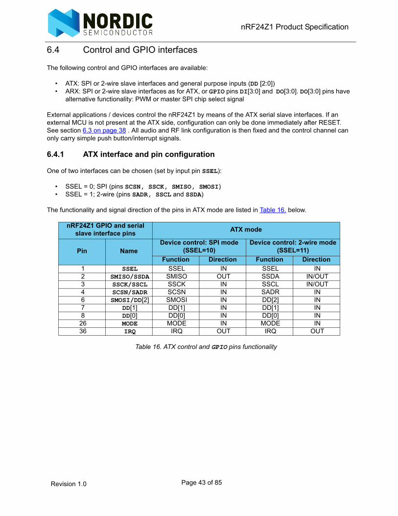
The following control and GPIO interfaces are available:
• ATX: SPI or 2-wire slave interfaces and general purpose inputs (DD [2:0])• ARX: SPI or 2-wire slave interfaces as for ATX, or GPIO pins DI[3:0] and DO[3:0]. DO[3:0] pins have
alternative functionality: PWM or master SPI chip select signal
External applications / devices control the nRF24Z1 by means of the ATX serial slave interfaces. If an external MCU is not present at the ATX side, configuration can only be done immediately after RESET. See section 6.3 on page 38 . All audio and RF link configuration is then fixed and the control channel can only carry simple push button/interrupt signals.
6.4.1 ATX interface and pin configuration
One of two interfaces can be chosen (set by input pin SSEL):
The functionality and signal direction of the pins in ATX mode are listed in Table 16. below.
Table 16. ATX control and GPIO pins functionality
nRF24Z1 GPIO and serial slave interface pins ATX mode
Pin NameDevice control: SPI mode
(SSEL=10)Device control: 2-wire mode
(SSEL=11)Function Direction Function Direction
1 SSEL SSEL IN SSEL IN2 SMISO/SSDA SMISO OUT SSDA IN/OUT3 SSCK/SSCL SSCK IN SSCL IN/OUT4 SCSN/SADR SCSN IN SADR IN6 SMOSI/DD[2] SMOSI IN DD[2] IN7 DD[1] DD[1] IN DD[1] IN8 DD[0] DD[0] IN DD[0] IN26 MODE MODE IN MODE IN36 IRQ IRQ OUT IRQ OUT
Page 43 of 85Revision 1.0
nRF24Z1 Product Specification
6.4.2 SPI slave interface
The first byte of the SPI transaction specifies the register address and whether it is a read or a write access. The seven least significant bits in the first byte is the nRF24Z1 register address, while the most significant bit is the read/write indicator (read=1, write=0), see Table 17.
Table 17. SPI command byte encoding
Write transaction: The next byte on SMOSI will be put into the register with the address specified in the first byte. Writing additional bytes will increment the register address automatically.
Read transaction: The next byte on SMISO will be the contents of the register with address as specified in the first byte. Reading more bytes will increment the register address automatically.
SCSN is active low. Consecutive accesses with SCSN low will auto-increment the address.
6.4.3 2-wire slave interface
This interface is similar to what is found on serial memories and data converter devices. The 7-bit device address of nRF24Z1 is ‘a101001’, where ‘a’ is the logic level of the SADR input pin (read during power-up and reset only).
Each 2-wire transaction is started with the “Start condition” followed by the first byte containing the 7 bit long device address and one read/write bit. This byte is hereafter referred to as the “address/read command byte” or the “address/write command byte” depending on the state of the read/write bit (read=1, write=0).
The second byte contains the register address, specifying the register to be accessed. This address will be written into the ATX chip, and it is therefore necessary that the first byte after the first start condition is an address/write command. Further actions on the 2-wire interface depend on whether the access is a read or write access. The 2-wire command byte is illustrated in Table 18.
Table 18. 2-wire command byte encoding
B7 B6 B5 B4 B3 B2 B1 B0R/W Register address
B7 B6 B5 B4 B3 B2 B1 B0a 1 0 1 0 0 1 R/W
Page 44 of 85Revision 1.0
nRF24Z1 Product Specification
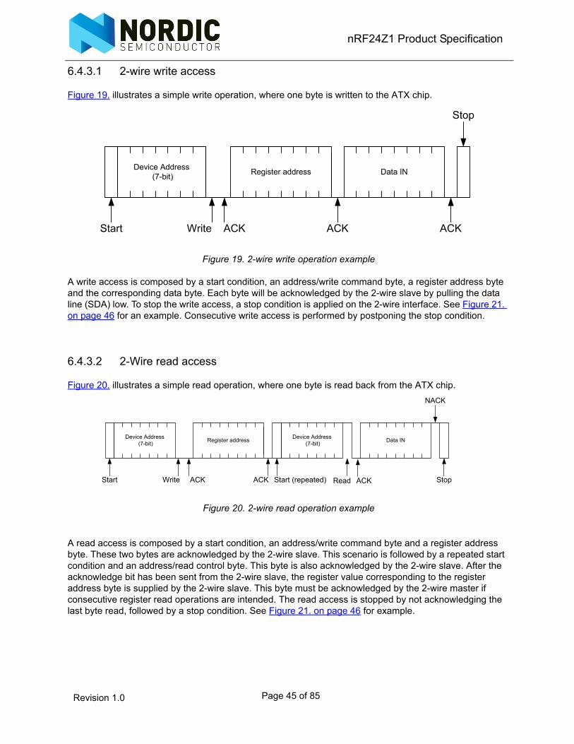
6.4.3.1 2-wire write access
Figure 19. illustrates a simple write operation, where one byte is written to the ATX chip.
Figure 19. 2-wire write operation example
A write access is composed by a start condition, an address/write command byte, a register address byte and the corresponding data byte. Each byte will be acknowledged by the 2-wire slave by pulling the data line (SDA) low. To stop the write access, a stop condition is applied on the 2-wire interface. See Figure 21. on page 46 for an example. Consecutive write access is performed by postponing the stop condition.
6.4.3.2 2-Wire read access
Figure 20. illustrates a simple read operation, where one byte is read back from the ATX chip.
Figure 20. 2-wire read operation example
A read access is composed by a start condition, an address/write command byte and a register address byte. These two bytes are acknowledged by the 2-wire slave. This scenario is followed by a repeated start condition and an address/read control byte. This byte is also acknowledged by the 2-wire slave. After the acknowledge bit has been sent from the 2-wire slave, the register value corresponding to the register address byte is supplied by the 2-wire slave. This byte must be acknowledged by the 2-wire master if consecutive register read operations are intended. The read access is stopped by not acknowledging the last byte read, followed by a stop condition. See Figure 21. on page 46 for example.
Device Address (7-bit) Register address Data IN
Write ACK ACK ACKStart
Stop
Device Address (7-bit) Register address Data IN
Write ACK ACK
NACK
Start Stop
Device Address (7-bit)
Start (repeated) Read ACK
Page 45 of 85Revision 1.0
nRF24Z1 Product Specification
Figure 21. 2-wire waveform example
6.4.4 General purpose input pins D[2:0]
Three (2 in the case of SPI slave being used, SSEL=0) general purpose inputs are available. The status on these pins can be read in register 0x20.
Table 19. ATX DD[2:0] status
If bit TXMOD[3] is set, the levels of pins DD[2:0] are mirrored on ARX pins DO[2:0] directly. See Table 10. on page 34.
The IRQ pin can act as an interrupt signal to external application circuitry. There are a number of interrupt sources available. See the chapter 8 on page 60 for details.
6.4.5 ATX control interface timing
6.4.5.1 2-wire slave timing
The interface supports data transfer rates of 100 kHz, 400 kHz and 1 MHz.
1 18 9 8 9
D7 D0 ACK D7 D0 ACK/NACK
Start condition
Stop condition
Address Hex Register R/W Description
0x75 TXDD R Value of ATX DD input pins Bit Interpretation 7:3 Reserved, do not use 2 Value of DD2 (only if SSEL=1) 1 Value of DD1 0 Value of DD0
Page 46 of 85Revision 1.0
nRF24Z1 Product Specification
Figure 22. 2-wire slave timing diagram
6.4.5.2 SPI slave timing
Normal SPI slave clock frequency is up to 8 MHz. However, at 3V (or higher) power supply, the maximum clock frequency may be increased to 16 MHz. Note the minimum pause interval tSRD between writing / reading of a byte.
Figure 23. SPI slave timing diagramTSSCK : SSCK cycle time.tdSSCK : time from SCSN active to first SSCK pulsetdSSPI : delay from negedge SSCK to new SMISO output datatsuSSPI : SMOSI setup time to posedge SSCKthdSSPI : SMOSI hold time to posedge SSCKtSRD : minimum pause between each byte read from or written to slave SPItSREADY : time from SSCK negative edge to SCSN rising edge
Refer to Table 41. on page 74 for more information.
tSW2_dsu
tSW2_od
SSCL
SSDA in
SSDA out
TSSCL
tSW2_dhd
tSW2_od
MSB
SSCK
SMISO
MSBSMOSI
tdSSCK
tdSSPI
tsuSSPI
thdSSPI
TSSCK
SCSN
MSBnext byteLSB
LSBMSB
next byte
tSRD tSREADY
Page 47 of 85Revision 1.0
nRF24Z1 Product Specification
6.4.6 ARX control interface options
The ARX is by default configured with a serial slave interface, identical to the ATX serial slave interface. The interface type (SPI or 2-wire) is selected by pin SSEL. The serial slave interface gives local access to all registers in the ARX, but no access to any registers on the ATX side. The only exceptions are RXPIN[3:0] and RXBUF (indirectly).
Alternatively, if RXSTA[6] is set in the configuration EEPROM, the ARX will be configured with GPIO pins instead of a serial slave interface. The pin-out and functionality of the slave interface or GPIO pins are shown in Table 21.
Table 20. ARX status register
RXSTA[6] cannot be updated from the ATX, but must be set by the EEPROM or by MCU at ARX side.
Table 21. ARX serial slave interface / GPIO configuration settings
Note: The GPIO functions described for registers RXPIO, RXPWME, RXPWMD, RXPIN bits 3:2, RXWAKE bits 3:2, are only available if the ARX is configured with GPIO interface (RXSTA[6]=1). However, these registers may always be read or written to, but if ARX is
Pin no
ARX with SPI slave interface (RXSTA[6]=0,
SSEL=0)
ARX with 2-wire slave interface (RXSTA[6]=0,
SSEL=1)
ARX GPIO interface (RXSTA[6]=1)
Function Direction Function Direction Function Direction1 SSEL IN SSEL IN DO[2] OUT
2 SMISO OUT SSDA IN/OUT DO[1] OUT
3 SSCK IN SSCL IN/OUT DO[0] OUT
4 SCSN IN SADR IN DO[3] IN6 SMOSI IN DI[2] IN DI[2] IN36 IRQ1
1. The ATX and ARX have their own local instance of the INTSTA register.
OUT IRQ OUT DO[3]/PWM2
2. General purpose output (DO[3]) or PWM functionality is set by register RXPWME (0x42).
OUT
Address Hex Register R/W Description
0x06 RXSTA R ARX status register. Bit Interpretation 7 RXEXEC status, 1 is OK, 0 is error 6 0 : ARX w. serial slave interface
1 : ARX w. GPIO interface, which implies no serial slave interface
5:0 Reserved, do not use
Page 48 of 85Revision 1.0
nRF24Z1 Product Specification
configured with slave interface, the registers will be disconnected from their corresponding GPIO-pins.
Note also that if ARX is configured with a slave interface, multiple ARX registers can be accessed both by the control channel from the ATX, and locally by the MCU via the slave interface. Care should be taken to avoid setting conflicting values to a register.
6.4.7 ARX GPIO pins
General purpose inputs DI[3:0] and outputs DO[3:0] are available in ARX-mode as shown in Table 21. on page 48.
6.4.7.1 Inputs
DI[3:0] are general purpose inputs while in ARX-mode. Status on these pins is monitored in ATX register RXPIN (0x07). If the ARX is configured with a slave interface, a connected MCU may emulate general purpose inputs by performing a local write to the RXPIN register.
Table 22. Register RXPIN (0x07)
6.4.7.2 Outputs
Configuration alternatives of general purpose pins DO[3:0] are shown below:
Table 23. DO [3:0] configuration alternatives
When used as general purpose outputs, DO[3:0] pin characteristics are controlled by register RXPIO (0x41). On some ARX general purpose output pins, high current drive capabilities can be enabled (for example, LED output driver). The register contents of RXPIO is listed in Table 24. on page 50.
Pins Functionality Controlling register DescriptionDO[3:0] General
purpose outputRXPIO (0x41) See below.
DO[2:0] Mirror of DD[2:0]
TXMOD (0x1A) See section 6.4.1 on page 43
DO[2:0] ARX SPI master bus
enable
RXDCMD (0x70) Table 14. on page 40
DO[3] PWM output RXPWME (0x42)RXPWMD (0x43)
See below.
Address Hex Register R/W Description
0x07 RXPIN R Current state of audio receiver GPIO inputs Bit Interpretation 7:4 Reserved, do not
use. 3 DI[3] value 2 DI[2] value 1 DI[1] value 0 DI[0] value
Page 49 of 85Revision 1.0
nRF24Z1 Product Specification
Table 24. Register 0x41 RXPIO
Values in RXPIO are sent to the ARX when (0x01) is written to RXCSTATE. Note that RXPIO values do not become effective until link is established. Example : initial values set in configuration EEPROM will not show on DO-outputs until link is established.
Pin DO[3] can also be used as a PWM output. PWM-enable and PWM-frequency is controlled by register RXPWME (0x42). PWM- duty cycle is controlled by register RXPWMD (0x43) as shown in Table 25.
Table 25. Registers RXPWME (0x42) and RXPWMD (0x43)
Values in RXPWME and RXPWMD are sent to the ARX when (0x01) is written to RXCSTATE.
Address Hex Register R/W Description
0x41 RXPIO R/W
Receiver GPIO output and drive strength Bit Logic 1 Interpretation 7 High drive high enable for DO[3] 6 Reserved, MBZ 1 5 High drive high enable for DO[1] 4 Reserved, MBZ 2 3 Data for DO[3] 2 Data for DO[2] 1 Data for DO[1] 0 Data for DO[0]
NOTES: 1: nRF24Z1 Version B : High drive low enable for DO[2] 2: nRF24Z1 Version B : High drive low enable for DO [0] High drive sink current (IOL_HD) for DO [0] and DO [2] @ VOL= 0.4V is typ. 10mA (only valid for nRF24Z1 Ver. B)
Address Hex Register R/W Description
0x42 RXPWME R/W Enables audio receiver PWM on pin DO[3] and sets PWM frequency
Bit Interpretation 7:6 00 : PWM not enabled
11 : Enable PWM on DO [3] 01,10 : reserved, do not use
5:0 PW M frequency (repetition rate) fPWM=16 MHz/(255⋅(1+RXPWME[5:0]))
0x43 RXPWMD R/W Set audio receiver PWM duty cycle
Page 50 of 85Revision 1.0
nRF24Z1 Product Specification
6.5 Data exchange between an ATX and ARX
To be able to exchange data an MCU is required on both ATX and ARX.
Before you can exchange data, the nRF24Z1 must be configured by an MCU. The RXMOD and TXMOD registers, in that order, must be written after all other configuration. The configuration of the ARX and ATX must be identical. If there are no ADC and DAC present during development, the I2SCNF_IN register can be set to 0x80 (master mode). This will ensure that the ATX and ARX can link up and exchange data even though no audio is present. The MCLK is not present until the link is up.
You can configure the nRF24Z1 from either an EEPROM or an MCU. Using an MCU to configure both the ATX and ARX is recommended to take advantage of all the features of the nRF24Z1. No EEPROM is needed when using an MCU, and the MMISO pin must be grounded for the nRF24Z1 to detect that no EEPROM is present.
Most configurations can be changed on the fly when using an MCU to configure the nRF24Z1, but there are some configurations related to audio interface, audio rate and latency that require forcing reconfiguration to enable them. This is controlled by writing to the LNKMOD register. The ARX and ATX then link up with the new setting and starts streaming audio again. You are recommended to mute the audio before you change the configuration.
There are several ways to exchange data between an ATX and ARX depending on the amount of data. There are two, typical ways to exchange data.
6.5.1 Exchanging a small amount of dataThe MCU on the ARX can write to the RXPIN register to transfer 1byte of data. The MCU on the ATX can either poll or set up a remote pin changed interrupt to detect that new data is present in the RXPIN register. This is a fast way to transfer small amounts of data from the ARX to the ATX, and the content of the RXPIN register is transferred in every data frame.
The MCU on the ATX can write to the RXPIO register to transfer 1 byte of data, followed by writing to the RXCSTATE. The MCU on the ARX can either poll or set up a remote pin changed interrupt to detect that new data is present in the RXPIO register.
Exchanging small amounts of data can be used as signal or indicate a button press between the two MCUs. This is the fastest way to transfer small amounts of data between the two devices.
6.5.2 Exchanging a large amount of data
The RXBUF register can be used to transfer up to16 bytes of data one way at a time and it must be initiated by the ATX. The RXWCNT and RXRCNT registers are set to the number of bytes to transfer and to which direction. The RXDCMD register must be set to 0x8E (no master interface access).
Finally the MCU on ATX writes to RXEXEC register, and then the RXBUF is transferred. The MCU on the ATX can poll RXEXEC to check for completion.
To signal that data is transferred you can use RXPIO or RXPIN registers as described in section 6.5.1.
An example of transferring large amounts of data are transferring song titles or artist names.
Page 51 of 85Revision 1.0
nRF24Z1 Product Specification
The following illustrates an example of transferring large amounts of data from the ATX to the ARX:
On the ATX side:
Write RXDCMD = 0x8E.
Write RXBUF data (up to 16 bytes).
Write RXWCNT = 16.
Write RXRCNT = 0.
Write RXEXEC = 1.
Wait to finish (poll RXEXEC register).
Now the RXBUF content is transferred from ATX to ARX, and the MCU on ARX should now be able to read out this register. The ATX can use the RXPIO register to signal to the ARX that new data is ready in RXBUF.
The following illustrates an example of transferring large amounts of data from the ARX to the ATX:
On the ARX side:
Write RXBUF data (up to 16 bytes).
Signal to ATX that data is ready to be transferred, using RXPIN register.
On the ATX side:
Write RXDCMD = 0x8E.
Write RXWCNT=0.
Write RXRCNT=16.
Write RXEXEC=1.
Wait to finish (poll RXEXEC).
Now the RXBUF content is transferred from ARX to ATX, and the MCU on ATX should be able to read out this data.
Page 52 of 85Revision 1.0
nRF24Z1 Product Specification
7 Quality of Service (QoS) and RF-protocol
The purpose of the QoS-engine is to maintain satisfactory audio quality across time, during normal operation.
This involves:
• Ensuring that corrupt or lost information sent from the ATX is automatically detected and retransmitted to the ARX
• Monitoring and avoiding channels used by other 2.4 GHz equipment or which have poor radio propagation properties (for example, fading effects)
• Reducing the audible effect of corrupt data when re-transmission fails within the latency time frame• Establishing a new link in the case of communication breakdown
The control channel is used to monitor radio-link status information.
It should be noted that at some point, the QoS-engine is unable to maintain a flawless audio link. This may be the result of stretched range, excessive interferer noise or both.
The RF-protocol is an integral part of the QoS-engine and is therefore not subject to user modification.
7.1 Link establishment
The link establishment procedure is fully managed on-chip.
7.2 RF protocol
The RF-protocol is controlled on-chip. The only parameter configurable by the application is the address. This enables separate nRF24Z1 devices to be identified and accessed independently in the same physical area. The RF protocol address length is 5 bytes and the address bytes are set in registers ADDR[0:4], listed in Table 26.
Table 26. RF protocol address
The contents of ADDR[0-4] ars sent to the ARX when (0x01) is written to LINKCSTATE.
Adaptive Frequency Hopping is an integral part of the QoS-engine functionality. The audio data is split in segments which are transmitted at different frequencies known by the transmitter and receiver. The frequencies used by the ATX/ARX are changing over time as active noise sources in the frequency band appear and disappear.
AFH also enables the nRF24Z1 link to handle challenges such as signal cancellation due to multi-path fading effects.
Page 54 of 85Revision 1.0
nRF24Z1 Product Specification
The frequencies used by the AFH-algorithm are specified in 38 frequency position registers shown in Table 27. The hopping sequence follows the register positions in consecutive order (meaning CH0, CH1, CH02.... CH36, CH37, CH0, CH1 and so on). The contents of CH0-37 may not be sent from the ATX to the ARX. Register values of CH0-37 must be configured locally by EEPROM or MCU.
Table 27. Frequency hopping table registers
Address Hex Register R/W Description0x0C CH0 R/W Frequency positions for the hopping
sequence. The frequency position frequency is equal to the position number multiplied by 1 MHz relative to 2400 MHz. Example: To define a frequency hopping scheme starting at f=2420 MHz, and then hopping to f=2440 MHz , the following values must be set : CH0=0x14, CH1=0x28...
In an environment without other 2.4 GHz applications or noise sources, the nRF24Z1 will use all the frequency positions listed in Table 27. on page 55. In the presence of an active RF system, occasional packet collisions are likely, resulting in RF packets being lost.
When an operating frequency resulting in unacceptable packet loss is detected, the ATX may remove it from the list of frequency positions used by AFH algorithm. The corresponding list in the ARX is synchronized by use of the control channel.
Frequency positions removed from the frequency hopping sequence are added to a FIFO list of frequencies temporarily banned for use by the AFH-algorithm.
The length of the list of banned frequencies are configurable (see Table 28.) The maximum number of banned channels is 18. A banned channel will remain in the list of banned frequencies until it will be pushed out by a new candidate.
The frequency bandwidth occupied by a nRF24Z1 device is approximately 4 MHz, whereas the frequency resolution of the available frequencies (frequency positions) is 1 MHz. Thus, the frequency position spacing in Table 27. must be at least 4 in order to achieve non-overlapping channels.
Note that the list of hopping positions does not need to contain solely non-overlapping channels in order to achieve optimal effect. Generally, the frequency positions should be distributed across the available frequency band.
Table 28. Frequency hopping configuration registers
Values in NBCH, NACK, and NLCH are transmitted to the ARX when 0x01 is written to RXCSTATE.
To minimize linking time, the same basic frequency hopping scheme must be set on the ATX and ARX side.
Address Hex Register R/W Description0x33 NBCH R/W Number of Banned Channels. The number of
frequency positions subject to ban at any time. Maximum register value is 18.
0x34 NACH R/W The number of frequency positions used in normal audio streaming mode. The frequency locations used are the first NACH-locations of Table 27. on page 55
0x35 NLCH R/W Number of frequency positions used in link mode. This is the number of frequency positions used in linking mode. The frequency locations used are the first NLCH-locations of Table 27. on page 55
Page 56 of 85Revision 1.0
nRF24Z1 Product Specification
7.4 Link registers
The nRF24Z1 has a number of link registers whose primary function is to monitor the overall quality on the link and enable actions to be taken based on it. The link monitoring registers are listed in Table 29.
Table 29. Link quality monitoring registersLNKQ and LNKERR are status registers directly available in the ATX. Note that only LNKERR is available inthe ARX.
The register value of LNKQ indicates the current level of strain on the QoS-engine. The LNKERR registerreports the number of unrecoverable packets in the last 14 frame window. LNKWTH and LNKETH registersenable system interrupts if one of the quality indicators drops below an acceptable level.
The link functional status is reported in register LNKSTA.
Actions to be taken upon the quality requirements set in LNKWTH and LNKETH, can be set in register LNKMOD. Registers LNKSTA and LNKMOD are listed in Table 30. on page 58.
Address Hex Register R/W Description
0x04 LNKQ LiNK Quality register. A measure of the number of packets lost in the last 14 frame window (of a consecutive series of 14 frame windows). Calculations :Number of packets lost in the 14 frame window is 255-LNKQ.LNKQ=255 means no packets lostTotal number of packets in the 14 frame window is (14*NPPF)+(255-LNKQ) where NPPF is Number of Packets Per Frame which varies with audio rate as shown below :
0x05 LNKERR R LiNK ERRor register. Returns the number of packets permanently lost1 in the last 32 frame window (of a consecutive series of 32 frame windows). 0 = no packets lost255 = all packets lost
1. A packet is permanently lost if it is not successfully received at the time itis required for audio output, meaning it can not be retransmitted any longer.
0x37 LNKWTH R/W LiNK Warning THreshold limit. A LNKQ value LNKWTH will cause an IRQ to be activated (if enabled by INTCF[5])
0x38 LNKETH R/W LiNK Error THreshold limit. A LNKERR value LNKETH will cause an IRQ to be activated (if enabled by INTCF[2])
Audio sampling rate
48-32kHz
24-16kHz
12-8kHz
NPPF 8 4 2
Page 57 of 85Revision 1.0
nRF24Z1 Product Specification
Table 30. Link status/mode registers
7.4.1 RF link latency
Link robustness may be traded with link latency. In systems where latency is not critical (like with music players), the high latency option should be used. Latency is set in the TXLAT register as shown below. Note that the resulting latency (for example, audio delay) also depends on the audio sampling rate fs.
Table 31. TXLAT register
Address Hex Register R/W Description
0x03 LNKSTA R/W Link status register Bit Interpretation 7:1 Reserved, do not use 0 Link established
0x36 LNKMOD R/W Link mode register. Bit Interpretation 7 Reserved, MBZ 6 ATX and ARX reset to initial EEPROM register
contents if no counterpart is found on the next link initialization.
5 Reserved, MBZ 4 Force reconfiguration with new configuration
data 3 Mute when LNKERR > LNKETH 2 Disable adaptive frequency hopping
1:0 Reserved, MBZ
Address Hex Register R/W Description
0x52 TXLAT R/W ATX to ARX Latency
Value Interpretation fs = 48kSPS
fs= 44.1kSPS
fs= 32kSPS
0 Short 6 ms 6.6 ms 9 ms 2 Nominal 11.4ms 12.4 ms 17 ms 4 High 16.7 ms 18.2 ms 25.1 ms
Note: Latency values listed are without ADC/DAC delay (digital in/out)
Page 58 of 85Revision 1.0
nRF24Z1 Product Specification
7.5 RF output power
The only configurable parameter in the RF subsystem is the RF transmitter output power. ATX output power is set in register TXPWR. ARX output power is set in register RXPWR.
Table 32. TXPWR and RXPWR registers
Both output power registers are accessible from the ATX. The output power on the ATX/ARX may thus be set based on the result of the RF link quality registers described in Table 29. on page 57 . Reducing the output power will result in extended battery lifetime and reduced strain on other coexisting RF systems.
Address Hex Register R/W Description
0x56 TXPWR R/W ATX output power Value Interpretation 0 -20 dBm 1 -10 dBm 2 -5 dBm 3 0 dBm
0x49 RXPWR R/W ARX output power Value Interpretation 0 -20 dBm 1 -10 dBm 2 -5 dBm 3 0 dBm
Page 59 of 85Revision 1.0
nRF24Z1 Product Specification
8 Interrupts
An nRF24Z1 with serial slave interface can be configured to deliver interrupts to any external system connected to pin IRQ. Interrupt sources are defined by register INTCF (0x13). Interrupt status flags are available in register INTSTA (0x02). After interrupt initiation, the IRQ will stay active (“0” with INTCF[7]=0, “1” with INTCF[7]=”1”) until a “1” is written to the corresponding interrupt flag in the INTSTA register. All interrupt flags may be cleared by writing 0x7F to INTSTA.
*ATX: interrupt generated by change of logic level on ARX DI[3:0]-pin(s). ARX: interrupt generated by change of logiclevel on ARX DO[3:0]-pin(s).
Table 33.Registers INTCF and INTSTA
Address Hex Register R/W Description
0x02 INTSTA R/W Interrupt status register. Register contents and interrupt are cleared upon reading.
Bit Interpretation 7 Reserved, do not use 6 link broken status flag 5 poor link quality status flag
(LNKQ<=LNKWTH) 4 remote transfer done status flag , set upon
completion of a RXEXEC, TXCSTATE, LNKCSTATE or RXCSTATE command.
3 ATX : remote input (RXPIN) changed status flag ARX with slave interface : RXPIO[3:0] register value changed status flag
2 Link error flag (LNKERR >= LNKETH) 1 Wakeup from power down status flag (see
section on “Interrupting an MCU while waking up:”)
0 Reserved, do not use See register INTCF for interrupt enabling
0x53 INTCF R/W Interrupt configuration. Select events that can generate interrupt on the IRQ pin. Bit Interpretation
7 Interrupt polarity, 1 is active high, 0 is active low
6 Enable link broken interrupt 5 Enable poor link quality interrupt 4 Enable remote transfer done interrupt 3 Enable GPIO changed interrupt * 2 Enable link error interrupt 1 Enable wakeup from power down
interrupt 0 Reserved, MBZ
Page 60 of 85Revision 1.0
nRF24Z1 Product Specification
An interrupt pin is always available in ATX mode. While in ARX mode, an interrupt pin is only availablewhen the device is configured with a serial slave interface. In this case the interrupt registers are local toATX and ARX respectively (meaning an interrupt on the ARX will only trigger the ARX, likewise an interrupton the ATX will only trigger the ATX).
If the nRF24Z1 is configured to give interrupt on “Wakeup from power down”, no other detected interruptswill trigger the IRQ pin. With this configuration, the IRQ pin will constantly be set active in power up andinactive in power down. This feature can be used by an external MCU to monitor the power down state ofthe nRF24Z1. “Poor link quality interrupt” and “Remote transfer done interrupt” are only available to theATX.
INTSTA- and INTCF register content is set locally in the ATX and the ARX devices. All interrupts must be cleared after power-on-reset.
Page 61 of 85Revision 1.0
nRF24Z1 Product Specification
9 RESET outputs
Designated pins not used for other functionality can provide reset pulses to external peripherals.
External RESET is required when the nRF24Z1 device is operated standalone and no autonomous devices (meaning MCU) are available to provide RESET to peripherals such as an ADC or DAC.
External RESET is executed as a part of the configuration routine performed immediately after power-on-reset and after device reconfiguration.
The I/O pin of choice and its signal polarity is dictated by register TXRESO (0x10) for the ATX and register RXRESO (0x40) for ARX peripherals.
Table 34. TXRESO and RXRESO registers
Values in the TXRESO and RXRESO registers should be stored in a configuration EEPROM.
Address Hex Register R/W Description
0x50 TXRESO R/W Enabling of optional RESET pulse output from ATX. Bit Interpretation 7:3 Reserved, MBZ 2:1
0 : no RESET output 1 : RESET output on MSDA pin 2 : RESET output on MOSI pin 3 : RESET output on SPDIO pin
0 ATX RESET output polarity 0 : active low 1 : active high Reset pulse duration is approx. 285 µs
0x40 RXRESO R/W Enabling of optional RESET pulse output from ARX. Bit Interpretation 7:3 Reserved, MBZ 2:1
0 : no RESET output 1 : RESET output on MSDA pin 2 : RESET output on MOSI pin 3 : RESET output on SPDIO pin
0 ARX RESET output polarity 0 : active low 1 : active high Reset pulse duration is approx. 285 µs
Page 62 of 85Revision 1.0
nRF24Z1 Product Specification
10 Power down control
10.1 Activation of power down mode
Two power down mode initiation alternatives exist; initiation by an external MCU or induced by detection of communication link breakdown/loss.
Normally, ATX/ARX power down is initiated by an external MCU connected to the ATX. The ARX power down mode is initiated first (register RXMOD[7]=1) followed by the ATX (register TXMOD[6]=1). Register TXMOD is described in Table 10. on page 34 and register RXMOD is described in Table 12. on page 36.
Note that the nRF24Z1s will not enter power down mode unless a wake time is specified. In order to enable ARX power down mode, the RXWTI register must contain a value > 0x00.
Similarly, the ATX TXWTI register value must be > 0x00. Refer to section 10.2.2 on page 64 for a timer control register description.
The ARX will enter power down as soon as the appropriate register settings have been successfully transferred. The transfer is initiated by writing 0x01 to register RXCSTATE.
10.1.1 Automatic power down
An automatic power down mechanism will be activated as soon as the nRF24Z1 looses its radio link. This mechanism will cause the nRF24Z1 to enter power down automatically if no new link is established after a specific timeout interval. This feature is enabled in the ATX by writing a value ≠ 0x00 into TXWTI and in the ARX by writing a value ≠ 0x00 into RXWTI. The time that the devices will spend looking for a link before going to automatic power down is specified by (TXSTI1 × 256 + TXSTI0) × 10 ms in the ATX and (RXSTI1 × 256 + RXSTI0) × 10 ms in the ARX.
10.2 Wake up from power down
Two events may trigger a wake up from power down mode; status change on external pin (wake-on-interrupt) and timer controlled wake up (wake-on-timer).
To deactivate power down mode, an external MCU is required to reset the power down bits in the ATX and ARX.
10.2.1 Wake-on interrupt
An nRF24Z1 device can be put in power down mode until the level on an external pin is changed. A change of logic level will initiate wake up and new link initialization.
In ATX mode, the DD[1] pin may be used to enable a wakeup. This feature is enabled in register TXMOD[5].
In ARX mode, wake up can be initiated by a level change on any of the input pins DI[3:0].
Wake up enable is controlled by register RXWAKE, described in Table 35. Register TXMOD is described in Table 10. on page 34.
Page 63 of 85Revision 1.0
nRF24Z1 Product Specification
Wake-on-timer has priority in this register. RXWAKE[4] must thus be cleared in order to enable external pin change wakeup. Any combination of the RXWAKE[0:3] bits can be set.
Upon wake up, the nRF24Z1 device will attempt to re-link during the specified wake time. If the power down bit is not reset during this interval the device will return to power down mode. Power down timing is described in sections 10.2.2 and 10.3. For external pin wakeup, the resulting wakeup time is TXWTI×(TXLTI+1)×10 ms for ATX and RXWTI×(RXLTI+1)×10 ms for ARX respectively.
The shortest pulse width (on an input pin) for wakeup is 1 ms.
Table 35. External wake-up control registers
10.2.2 Wake-on timer
The nRF24Z1 can also be operated in a power saving mode where timers controls a cyclic power down / wake up sequence. In this mode the nRF24Z1 will be able to re-initialize the RF link without any user interaction. If no matching nRF24Z1 devices are located within the specified time interval after wake-up, power down mode is resumed.
The internal timer that puts the device into the power down part of the cycle has priority over link re-initialisation attempts. In order to re-initialize the link, the power down bits in TXMOD and RXMOD must be cleared during the wake up part of the cycle, and the ATX and ARX must both be in the wake up part of the cycle at the same time. Power down is resumed if RXMOD and TXMOD power down bits remain set, or if ATX and ARX are not in the wake up part of the cycle at the same time.
In power down mode, the ATX and ARX timing is no longer synchronized. A separate set of timers are hence implemented in the ATX and ARX.
The wake-on-timer sequence is controlled by a 16 bit sleep interval timer (ATX: TXSTI, ARX: RXSTI) and an 8 bit wake up interval timer (ATX: TXWTI, ARX: RXWTI). The contents of the sleep timer control registers decide the number of consecutive 10 ms intervals the nRF24Z1 device will sleep before waking up. The wake up interval timers correspondingly sets the number of consecutive 10 ms intervals in which the nRF24Z1 should attempt to re-link before returning to power down mode.
If the two paired nRF24Z1 devices are active at the same time, and the power down bits in TXMOD and RXMOD are cleared, a link is re-established. The controlling device (for example, MCU) on the ATX side should then reset TXWTI and RXWTI in order to prevent return to power down mode caused by the automatic power down mechanism. With a controlling MCU on the ATX side, it is important to put the ARX to sleep before the ATX, and to wake up the ATX before waking up the ARX.
Address Hex Register R/W Description
0x45 RXWAKE R/W Wakeup sources for audio receiver Bit Interpretation 7:6 Reserved, MBZ 5 Reserved 4 Wakeup on sleep timer 3 Wakeup on DI[3] change 2 Wakeup on DI [2] change 1 Wakeup on DI [1] change 0 Wakeup on DI [0] change
Page 64 of 85Revision 1.0
nRF24Z1 Product Specification
The sleep and wake up timers are controlled by the registers described in Table 36.
Table 36. Sleep and wake-up timer registers
10.2.3 Wakeup from automatic power down
When automatic power down is enabled, and after having lost its link for the specified time, the devices will enter the sleep modes set by TXMOD, RXMOD and RXWAKE. This means that a device set to Wake-on-Interrupt has to be interrupted (meaning button is pushed) before it may start trying to re-establish a link after automatic power down. However, if both ATX and ARX are set to Wake-on-timer, they are able to wake up from automatic power down without user intervention.
Address Hex Register R/W Description
0x57 TXSTI[0] R/W ATX sleep timer byte #0 TXSTI is a 16-bit number specifying the number of consecutive 10ms periods in which the ATX is to sleep between attempts to establish a new link.
0x58 TXSTI[1] R/W ATX sleep timer byte #1 0x59 TXWTI R/W ATX wake up timer. With TXWTI set to 0, the ATX will not
return to power down mode. A setting > 0 will specify the number of consecutive 10 ms periods in which the ATX is trying to establish a link before re-entering power down mode.
0x4D TXLTI R/W ATX wake up time extension register, used to extend ATX wake up time when woken by a pin status change or while in link mode. Total wake up time is then (TXLTI+1) ×TXWTI×10 ms
0x46 RXSTI[0] R/W ARX sleep timer byte #0 RXSTI is a 16-bit number specifying the number of consecutive 10ms periods in which the ARX is to sleep between attempts to establish a new link. Only used if the sleep timer is enabled, see bit 4 of RWAKE register.
0x47 RXSTI[1] R/W ARX sleep timer byte #1 0x48 RXWTI R/W ARX wake up timer. With RXWTI set to 0, the ATX will not
return to power down mode. A setting > 0 will specify the number of consecutive 10 ms periods in which the ARX is trying to establish a link before re-entering power down mode.
0x4C RXLTI R/W ARX wake up time extension register, used to extend ARX wake time when woken by a pin change or while in link mode. Total wake time is then (RXLTI+1)×RXWTI×10 ms
Page 65 of 85Revision 1.0
nRF24Z1 Product Specification
10.2.4 Interrupting an MCU while waking up
The nRF24Z1 has several ways of interrupting an external MCU or other external devices. The wakeup from power down interrupt (INTSTA[1]) is the only interrupt whose interrupt flag does not have to be cleared in register INTSTA. Enabling the wakeup from power down interrupt on the ATX makes the IRQ output pin track the sleep modes of the nRF24Z1. An active low IRQ pin will be low when the ATX is streaming audio or trying to establish a link. It will be high when the ATX is idle between attempts at establishing a link.
This means that if the ATX is Wake-on-Timer, the external MCU does not have to be in charge of system timing while in sleep mode. Instead it is interrupted by the nRF24Z1 whenever it wakes up and becomes ready to receive commands.
10.3 nRF24Z1 power saving example
A combination of the two power down control alternatives is possible. Figure 24. shows an example of ATX timer controlled power down combined with power down with wake up on external pin event in the ARX. In this example the ARX is shut down completely until a user activates the ARX (meaning headphone or speaker).
Figure 24. nRF24Z1 power saving example
In this example, the ARX will wake up upon a logic level shift on one of the DI[3:0] pins. The ARX will then be active for the designated time interval, attempting to establish link with the ATX. The ARX will return to power down if the register bit RXMOD[7] is not cleared.
The ATX will wake up from power down on a cyclic basis. In order to (cancel cyclic behaviors) the ATX, the register bit TXMOD[6] must be cleared within the ATX wake time.
If the ARX wakes up and a link is established, the ARX and ATX will remain awake upon ATX clearing of the ARX power down bit.
ATX will resume power down if no link is found after the extended wake time interval is over; even when the power down bit was cleared.
TXWTI
MCU initiates power down on ATX
MCU on ATX initiates ARX resumes power- down.
ATX and ARX power down bits reset by MCU
ATX power- up ATX power-down
ARX power- up ARX power-down
ARX wakes up from pin change
ARX wakes up from pin change
TXWTI
TXSTI TXSTI TXSTI
RXWTI * (RXLTI+1)
ATX wakes up from timer
Link found, power down disabled
If no link is established, the ATX will resume power down automatically
TXWTI * (TXLTI+1)
power down on ARX
Page 66 of 85Revision 1.0
nRF24Z1 Product Specification
11 Register update over the control channel
The registers TXCSTATE, LNKCSTATE, RXCSTATE can be used by an ATX MCU to update audio receiver control registers through the control channel. Writing to these registers from an ARX MCU is illegal. When the ATX MCU is to initiate a register contents change in one or more of the ARX registers, the register value(s) are first buffered in the ATX. The registers’ contents are then transferred to the ARX and employed there when the corresponding update register is written to by the ATX MCU. Prior to any transfer to the ARX, the transfer register should be polled to check if the ATX is ready to transfer new register values to the ARX.
Setting an update register to 0x01, triggers the ATX to send the corresponding register values to the ARX. The update register is then automatically reset to 0x00 after the register values have been successfully transferred. When an update register reads 0x01, the ATX is busy sending the register values to the ARX. When an update register reads 0x02, the last transfer was unsuccessful. A value of 0x02 may indicate a radio link problem.
Page 67 of 85Revision 1.0
nRF24Z1 Product Specification
Table 37. Register update registers
11.1 Register update and device relinkSome register updates require ARX and ATX reconfiguration.
The ATX and ARX will always be reconfigured after a link has been established. The ATX and ARX may thus be reconfigured by forcing a re-link. This can be done by setting the “Force reconfiguration” bit; LNKMOD[4] = 1.
AddressHex
Register R/W Description
0x5B TXCSTATE R/W Controls when to send ATX registers TXFMT,TXLAT,I2SCNF_IN over the data link to the ARX. Status values are :
0 : idle, last transfer successful1 : busy, registers may not be accessed. 2 : idle, last transfer unsuccessful
When idle, data may be written to the ATX registers.Setting TXCSTATE=1 triggers the ATX to send register values tothe ARX. TXCSTATE is automatically reset to 0 by the ATX uponsuccessful transfer to the ARX. An external MCU should pollthis register before accessing the ATX registers.
0x3E LNKCSTATE R/W Controls when to send ATX side link control registers over thedata link to the ARX. Status values are :
0 : idle, last transfer was successful1 : busy, registers may not be accessed2 : idle, last transfer was unsuccessful
When idle, data may be written to the link control registers.Setting LNKCSTATE=1 triggers the ATX to send link controlregister values to the ARX. LNKCSTATE will be reset to 0 by theATX upon successful transfer to the ARX. An external MCUshould poll this register before accessing any link controlregisters.
0x4B RXCSTATE R/W Controls when to send ARX control register data from the ATXover the data link to the ARX. Status values are1 :
0 : idle, and last transfer was successful1 : busy, the registers may not be accessed2 : idle, but last transfer was unsuccessful
When idle, data may be written to the ARX control registers.Setting RXCSTATE=1 triggers the ATX to send ARX controlregister values to the ARX. RXCSTATE will be reset to 0 by theATX upon successful transfer to the ARX. An external MCU should poll this register before accessing anyof the ARX control registers.
1. Status applies to all ARX control registers except RXMOD
LINK registers ADDR0,ADDR1,ADDR2, ADDR3,ADDR4NBCH,NACH
TEST_MODE registers
TESTREG,TESTCH
Register name Register functionRXSTA[6] The ARX serial slave interface may only be disabled by setting
RXSTA[6] from an external configuration EEPROM. A serial slave interface will be enabled by default if no EEPROM is present on the ARX.
CH0-37 The frequency hopping table registers is not transferred from the ATX to ARX. These registers must therefore be configured in EEPROM or local MCU.
TXSTA Sampling rates are automatically transmitted to the ARX from the ATX during link-locate mode.
RXMOD ARX operation mode are automatically transmitted to the ARX from ATX during link-locate mode.
RXPIN Information about ARX general-purpose input pins is automatically transmitted from the ARX to the ATX during link-locate mode. This information is also being continuously transferred from the ARX to the ATX during normal audio streaming mode.
TXCSTATE Transfer register used by the ATX to send data to ARXRXCSTATE Transfer register used by the ATX to send data to ARXLNKCSTATE ransfer register used by the ATX to send data to ARXRXEXEC Transfer register used by the ATX to send and receive data to/
from the SPI and 2-wire master interfaces of the ARX
Page 69 of 85Revision 1.0
nRF24Z1 Product Specification
12 Test modenRF24Z1 test mode is initiated by writing to test registers TESTREG and TESTCH, followed by setting bit 4of the LNKMOD register. This will force the device to restart in test mode according to the TESTREG andTESTCH register settings.
nRF24Z1 will remain in test mode until reset. Test mode can only be aborted by use of reset. Test modechanges can only be performed upon device reset. This applies for both the ATX and ARX.
The ATX test registers can be accessed through the (SPI or 2-wire) slave interface (also valid for an ARXconfigured with slave interface; RXSTA[6]=0).
For an ARX configured from an external EEPROM with GPIO interface (EEPROM/RXSTA[6]=1), the slave interface does not exist, blocking access to the test registers. EEPROM configuration may be avoided by forcing the EEPROM data output line low, aborting the read process from the EEPROM. As a result, RXSTA[6] will not be set, and the ARX is configured with a slave interface.
Table 40. Test mode registers
Note: Output power in test mode is always 0 dBm, and any other setting in TXPWR and RXPWR registers is ignored in test mode.
Address Hex Register R/W Description
0x7E TESTREG W Test mode register: Code 1: 0110 0011 – Single channel test. Code 2: 0111 0011 – Channel sweep test. Sweeps all channels from frequencies from 2400 MHz to 2480 MHz in steps of 1 MHz.
0x7F TESTCH W Bit Interpretation 7 1: TX, 0: RX
Initiates the mode described in TESTREG in RX / TX mode.
6:0 Channel number when TESTREG is set to Code 1 (single channel), number is in 1 MHz step relative to 2400 MHz
Page 70 of 85Revision 1.0
nRF24Z1 Product Specification
S
Oper
Digita
Digit
I
Gene
Gene
RB
Δ
RF trPR
PR
PR
PR
P
13 Electrical specifications
ymbol Parameter (condition) Notes Min. Nom. Max. Units
ating conditionsVDD Supply voltage 2.0 3.0 3.6 V
TEMP Operating temperature -20 27 80 ºCl input pinsVIH HIGH level input
voltage 0.7 ×VDD VDD V
VIL LOW level input voltage
VSS 0.3×VDD V
al output pinsVOH HIGH level output
voltage (IOH=-0.5mA)VDD-0.3 VDD V
VOL LOW level output voltage (IOL=0.5mA)
VSS 0.3 V
OH_HD High drive source current for DO[1] and DO[3] @ VOH= VDD-
0.4V
1 10 mA
ral electrical specificationIPD Supply current in
power down mode5 µA
ral RF conditionsfOP Operating frequency 2 2400 2521 MHzΔf Frequency deviation +/-640 kHz
GFSK GFSK data rate 4000 kbpsWMOD Modulation bandwidth 4 MHzfXTAL Crystal frequency 3 16 MHzCload Crystal load
capacitance3 8 12 16 Pf
fXTAL X-tal frequency tolerance +
temperature drift
3 +/-30 ppm
ansmit modeF_0dBm Maximum output
power (TXPWR=3)4 0 3 dBm
F_-5dBm Maximum output power (TXPWR=2)
4 -5 0 dBm
F_-10dBm Maximum output power (TXPWR=1
4 -10 -5 dBm
F_-20dBm Maximum output power (TXPWR=0)
4 -20 -12 dBm
PRFC RF power control range
16 20 dB
RFCR RF power range control resolution
+/-3 dB
PBW 20dB bandwidth for modulated carrier
2500 4000 kHz
Page 71 of 85Revision 1.0
nRF24Z1 Product Specification
RF reR
R
ATX IA
I
IAT
IAT
IAT
ARXIA
I
I2S i
S
ceive modeXSENS Sensitivity at 0.1%
BER-80 dBm
XMAX Maximum received signal
0 dBm
current consumptionTX_0dBm Mean supply current
in audio streaming mode @ 0dBm output power Sample rate:32kSPS44.1kSPS48kSPS
5 141718
mAmAmA
ATXmax Peak supply current inaudio streaming modefor all sample rates and output power
5 33.5 mA
X_-5dBm Mean supply current @ -5dBm output power
67
16 mA
X_-10dBm Mean supply current @ -10dBm output power
15.3 mA
X-20dBm Mean supply current @ -20dBm output power
15 mA
current consumptionRX_lnk Mean supply current
in link mode 32 mA
ARX_au Mean supply current in audio streaming mode Sample rate:32kSPS44.1kSPS48kSPS
89
19.52324
mAmAmA
nterface timing (see Figure 13. on page 37, Figure 14. on page 37 and Figure 15. on page 38.TI2S I2S clock period 150 ns
DATA and WS (input) setup time to CLK
20 ns
DATA and WS (input) hold time from CLK
20 ns
DATA and WS (output) delay from CLK
40 ns
ymbol Parameter (condition) Notes Min. Nom. Max. Units
Page 72 of 85Revision 1.0
nRF24Z1 Product Specification
MCL
Δ
Slav
t
t
t
tS
MastTt
t
t
SlavT
tM
tM
tM
MastT
tM
tM
tM
1
S
K (256 fs) output clock
fMCLK Locking range vs nominal MCLK frequency
10 -500 +500 ppm
JRMS RMS jitter 0-25kHz 250 310 pse SPI interface timing (See Figure 23. on page 47)TSSCK SSCK clock period 11 62 nssuSSPI SMOSI setup time to
SSCK10 ns
hdSSPI SMOSI hold time from SSCK
10 ns
tdSSPI SMISO delay from SSCK
55 ns
dSSCK SCSN setup time to SSCK
500 µs
tSRD SPI slave ready 500 µsREADY SCSN hold time to
SSCK500 µs
er SPI interface timing (see Figure 18. on page 42)MSCK MSCK clock period 125 ns
suMSPI MMISO setup time to MSCK
55 ns
hdMSPI MMISO hold time from MSCK
10 ns
tdMSPI MMOSI delay from MSCK
20 ns
dMSCK MCSN setup to MSCK
30 500 ns
e 2-wire interface timing (see Figure 22. on page 47)MSCL 2-wire clock period 1000 nsW2_dsu MSDA setup time to
MSCL60 ns
W2_dhd MSDA hold time from MSCL
50 ns
W2_od MSDA 1->0 delay from MSCL
50 ns
er 2-wire interface timing (see Figure 17. on page 42)MSCL 2-wire clock period 1000 nsW2_dsu MSDA setup time to
MSCL60
W2_dsd MSDA hold time from MSCL
50 ns
W2_od MSDA 1->0 delay from MSCL
50 ns
. Output pin programmed for high current (register RXPIO).
ymbol Parameter (condition) Notes Min. Nom. Max. Units
Page 73 of 85Revision 1.0
nRF24Z1 Product Specification
2.3.4.56.7.8.9.1011
Table 41. nRF24Z1 Electrical specifications
Device operates in the 2400 MHz ISM band (2400-2483 MHz).For further details on crystal specification, see section 17.2 on page 78.Antenna load impedance = 100W+j175W, see chapter 17 on page 78.
. Cload_MCLK ≈8pFSample rate=44.1 kSPSCload_MCLK≈8pFCCLK=CWS=CDATA=CMCLK≈10pFPeak current in ARX-mode is approximately 34mA. Nominal MCLK frequency is 256 times fs for fs in [32 kHz, 44.1 kHz, 48 kHz] programmable. For VDD≥3.0V +/-10%, otherwise minimum TSSCK is 124 ns (8 MHz)
Page 74 of 85Revision 1.0
nRF24Z1 Product Specification
14 Absolute maximum ratings
Maximum ratings are the extreme limits to which the device can be exposed without permanently damaging it. Exposure to absolute maximum ratings for prolonged periods of time may affect device reliability.
The device is not guaranteed to operate properly at the maximum ratings.
Note: Stress exceeding one or more of the limiting values may cause permanent damage to the device.
Operating conditions Range Units
Supply voltagesVDD -0.3 to 3.6 VVSS 0 V
Input voltageVI -0.3 to VDD +0.3 VVO -0.3 to VDD +0.3 V
Output voltageVO -0.3 to VDD +0.3 V
TemperaturesOperating
temperature-20 to +80 °C
Storage temperature
-40 to +125 °C
Attention!Observe precaution for handling Electrostatic Sensitive Device. HBM (Human Body Model): Class 1A
B Build Code, that is, unique code for production sites, package type and test platform. Variable.
X “X” grade, that is, Engineering Samples (optional). Variable.
YY Two-digit Year number. Variable.WW Two-digit Week number. Variable.LL Two-letter wafer lot number code. Variable.
Page 77 of 85Revision 1.0
nRF24Z1 Product Specification
17 Application information
17.1 Antenna I/OThe ANT1 & ANT2 output pins provide a balanced RF output to the antenna. The pinsmust have a DC path to VDD_PA, either via a RF choke or via the center point in abalanced antenna. Differential load impedance between the ANT1 and ANT2 pins,100Ω+j175Ω, is recommended for maximum output power. Antennas with lower loadimpedance (for example 50 Ω) can be matched to nRF24Z1 by using a simple matchingnetwork.
17.2 Crystal specification
Tolerance includes initial accuracy and tolerance over temperature and aging.
Table 45.Crystal specification of nRF24Z1In order to obtain a crystal setup with low power consumption and fast start-up time, a crystal with lowcrystal load capacitance is recommended.
The crystal load capacitance, CL, is given by:
C1 and C2 are SMD capacitors as shown in the application schematics. CPCB1 and CPCB2 are the layout parasitics on the circuit board. CI1 and CI2 are the capacitance seen into the XC1 and XC2 pin respectively; the value is typical 1pF.
17.3 Bias reference resistor
A resistor between pin IREF (pin 24) and ground sets up the bias reference for the nRF24Z1. A 22 kΩ (1%) resistor is to be fitted. Changing the value of this resistor will degrade nRF24Z1 performance.
17.4 Internal digital supply de-coupling
Pin DVDD (pin15) is a regulated output of the internal digital power supply of nRF24Z1. The pin is purely for de-coupling purposes and only a 33nF (X7R) capacitor is to be connected. The pin must not be connected to external VDD and can not be used as power supply for external devices.
17.5 PCB layout and de-coupling guidelinesA well-designed PCB is necessary especially to achieve good RF performance. Keep in mind that a poor layout may lead to loss of performance, or even functionality if due care is not taken. A fully qualified RF-layout for the nRF24Z1 and its surrounding components, including antenna matching network, can be downloaded from www.nordicsemi.com.
Frequency CL ESR C0max Tolerance16 MHz 8pF to 16pF 100Ω 7.0pF +/-30 ppm
2222111121
21 '',''''
IPCBIPCBL CCCCandCCCCwhereCCCC
C ++=++=+⋅
=
Page 78 of 85Revision 1.0
nRF24Z1 Product Specification
A PCB with a minimum of two layers with ground planes is recommended for optimum performance. The nRF24Z1 DC supply voltage must be de-coupled as close as possible to the VDD pins, see chapter 18 on page 80. A large value surface mount tantalum capacitor (for example 10µF) should be placed in parallel with the smaller value capacitors. The nRF24Z1 supply voltage must be filtered and routed separately from the supply voltages of other circuitry. When the nRF24Z1 is used in combination with A/D and D/A converters, it is very important to avoid power supply noise generated by the nRF24Z1 from reaching the analogue supply pins of the A/D and D/A converters. Hence, star-routing directly from a low-noise supply source (like a linear voltage regulator) is highly recommended, and where the nRF24Z1 has its own power supply line from the supply source and also the A/D and D/A converters have their own separate digital and analogue supply lines.
Long power supply lines on the PCB should be avoided. All device grounds, VDD connections and VDD bypass capacitors must be connected as close as possible to the nRF24Z1 IC. For a PCB with a topside RF ground plane, the VSS pins should be connected directly to the ground plane. For a PCB with a bottom ground plane, the best technique is to place via holes as close as possible to the VSS pins. A minimum of one via hole should be used for each VSS pin.
Full-swing digital data or control signals should not be routed close to the reference crystal or the power supply lines.
Page 79 of 85Revision 1.0
nRF24Z1 Product Specification
18 Reference circuits
The following example show nRF24Z1 schematics and layouts where the ATX is controlled over SPI by an external MCU and the ARX has a SPI EEPROM attached for stand alone operation.
Resistors R3 and R4 are not necessary for device functionality. R3 is added to guarantee that no nRF24Z1 registers are changed if the external MCU is resetting. R4 is used to terminate the nRF24Z1 SPI input.
!"#$
%&'()
'&&'()
&&'()
"&&()
'&()&()
()&()
()&()
%!
*'
+
+
* " " * % '%
"
'
'
!&'()&*
, -
+
.
.
.
'
"'
!
/
Page 80 of 85Revision 1.0
nRF24Z1 Product Specification
This avoids any floating signals if the SPI bus is disabled (power down). Only one resistor on the bus is needed. If the MCU MOSI output has internal pull up/down, it can be omitted.
1. Inductance versus frequency may differ significantly in inductors with the same value but withdifferent part numbers and/or vendors! Inductor value is usually characterized at 100-250 MHz, butthe actual value at 2.4 GHz may vary significantly even though the given inductance at 250 MHz isthe same. Inductors from other TOKO series and other vendors may well be used, but antennamatching network performance MUST be verified as the inductor value may need to be changed.
1. Inductance versus frequency may differ significantly in inductors with the same value but different part numbers and/or vendors! Inductor value is usually characterized at 100-250 MHz, but the actual value at 2.4 GHz may vary significantly even though the given inductance at 250 MHz is the same. Inductors from other TOKO series and other vendors may well be used, but antenna matching network performance MUST be verified as the inductor value may need to be changed.
Term DescriptionADC Analog to Digital ConverterAFH Adaptive Frequency HoppingARX Audio ReceiverATX Audio TransmitterBER Bit Error RateBoM Bill of MaterialsCD Carrier Detect
CPHA SPI Clock PhaseCLK Clock
CPOL SPI Clock PolarityCRC Cyclic Redundancy CheckCSN Chip Select NotDAC Digital to Analog ConverterDSP Digital Signal Processor
EEPROM Electrical Erasable Programmable Read Only Memory
FIFO First In First OutFlash Flash MemoryGFSK Gaussian Frequency Shift KeyingGPIO General Purpose In Out I2S 3-wire audio serial interfaceISM Industrial-Scientific-Medical
kSPS kilo Samples Per SecondLatency Audio delay from ATX input to ARX outputLPCM Linear PCM (pulse code modulation)LSB Least Significant BitMbps Megabits per secondMBZ Must Be ZeroMCU Micro Controller UnitMP3 MPEG3, audio compression formatMSB Most Significant BitPCB Printed Circuit BoardPWM Pulse Width ModulationQoS Quality of ServiceRX Receive
S/PDIF One-wire serial digital audio formatSPI Serial Peripheral Interface TX Transmit
2-wire 2-wire serial interface compatible with I2C