Nanotechnology Newsletter IEEE nanotechnology Council June 2010 I NSIDE T HIS I SSUE 1 President’s message p1 2 IEEE NMDC 2010 p2 3 IEEE NANO 2009 (highlights) p3 4 IEEE Distinguished lecturer program p4-p5 5 Research Highlights Patterned Media p6-p8 NanoElectrodes p9-p11 6 Vision of Nanotechnology NanoRobots p12-p14 7 Nanotechnology Awards p15-p17 8 Featured Journal p18 9 IEEE NTC Members p19 10 IEEE AdCom NTC Member Election p20 11 IEEE NANO conference (2010) p21 12 Students’ corner p22 13 Upcoming Events p23
Transcript
Nanotechnology Newsletter
IEEE nanotechnology Council
June 2010
I N S I D E T H I S I S S U E 1 President’s message p1
2 IEEE NMDC 2010 p2
3 IEEE NANO 2009
(highlights) p3
4 IEEE Distinguished lecturer program p4-p5
5 Research Highlights
Patterned Media p6-p8 NanoElectrodes p9-p11
6 Vision of Nanotechnology
NanoRobots p12-p14
7 Nanotechnology Awards p15-p17
8 Featured Journal p18
9 IEEE NTC Members p19
10 IEEE AdCom NTC Member Election p20
11 IEEE NANO conference (2010) p21
12 Students’ corner p22
13 Upcoming Events p23
1 NTC IEEE Nanotechnology Newsletter June, 2010
President’s Message
Dear IEEE NTC members,
I have been elected as the new IEEE Nanotechnology Council President and will serve the Council from January 1, 2010 to December 31, 2012. Currently I am the John D. Ryder Professor of Electrical and Computer Engineering in the Department of Electrical and Computer Engineering and the Director of Robotics and Automation Laboratory at Michigan State University.
As the president I intend to lead the Council to better serve its members. The major goals I look forward are to enhance the technical spectrum of the IEEE Nanotechnology Council, to increase its industrial participation, and to strengthen the financial standings of the Council. The specific endeavors I strive to complete in the next two years include, further improvement of the publications of IEEE
Transaction on Nanotechnology and IEEE Nanotechnology Magazine, working with other IEEE societies to develop more conferences, workshops and symposiums in the areas most representative of nanotechnologies and to develop the nanotechnology lecture series to promote the research, development, and education of the nanotechnology, and to reach out to industries and general public. The success of these efforts will enable the IEEE Nanotechnology Council to be financially viable, and promoting it to become the premier professional organization of nanotechnology in the world.
I welcome you all to provide new ideas and suggestions to improve IEEE Nanotechnology Council and its activities and productivities.
Dr. Ning Xi 2120 Engineering Building Michigan State University East Lansing, MI 48824, USA
From the Editor
Welcome to the June 2010 issue of the NTC IEEE Nanotechnology Newsletter. I am John Yeow from the Waterloo Institute of Nanotechnology at the University of Waterloo, Ontario, Canada where I am currently a Canada Research Chair in Micro/Nanodevices and Director of the Advanced Micro/Nanodevices Lab.
I was invited by Dr. Chennupati Jagadish and Dr. Meyya Meyyapan to be the Editor-in-Chief of the NTC IEEE Nanotechnology Newsletter. It is a position I gladly accepted because this position allows me to get in touch with many of you within the nanotechnology community. It is also my role to keep you updated on the latest nanotechnology trends and development, be it commercial or research. Throughout the year, I look forward to working with Dr. Ning Xi who is the current President of the Council in bringing you exciting new issues of the newsletter.
The goal is to provide 4 issues of newsletter annually. I seek your inputs in terms of interesting articles, news, announcements, and commentaries. If you have ideas to share, please email me at jyeow [at] engmail [.] uwaterloo [.] ca
Sincerely, Dr. John T.W. Yeow University of Waterloo 200, University Avenue West Waterloo, ON, Canada
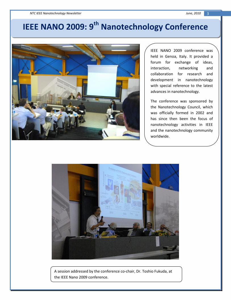
A session addressed by the conference co-chair, Dr. Toshio Fukuda, at
the IEEE Nano 2009 conference.
4 NTC IEEE Nanotechnology Newsletter June, 2010
IEEE Distinguished Lecturer Program
IEEE Distinguished Lecturers are engineering professionals who help lead their fields in new technical developments that shape the global community. These experts:
specialize in the field of interest of their Society/Council.
travel to various technical and regional groups to lecture at events.
Robustness and efficiency of the nanoelectrodes can
be enhanced through optimal alignment of
nanoelectrode arrays by appropriate fabrication
techniques. Spatially separated geometry of
nanoelectrode arrays have shown to enhance protein
immobilization on each electrode [12, 13]. Moreover,
high precision linkage between the analyte and the
electrodes collectively contribute to enhanced
detection limits of the nanoelectrodes in comparison to
macro or microelectrodes [2].
Integration of nanostructures into micro-devices is not
trivial and requires implementation of innovative
strategies for nanomaterial deposition and processing
[9]. Moreover, some nanoscale material properties,
particularly, the electrical conductivity has been noted
to reduce drastically with decreasing size. The inverse
correlation between size and conductivity specifically
restricts further downscaling of electronic components
in applications wherein electrical conductivity is
paramount for device performance [9]. Fabrication of
nanoelectrodes is one of the greatest challenges faced
by researchers [1]. Reduction in electrical conductivity
of nanoscale structures, due to increased surface
energy barriers and density of boundaries, adds to the
challenge especially when they need to be integrated
with standard electronic components [9]. Typically,
electrodes in micro- and nanosensors are made of
dense films that are deposited by chemical vapour
deposition, sputtering, screen printing, etc. In general,
a functional nanofilm (a sensing material) is deposited
between these electrodes, or the electrodes
themselves are functionalized to act as nanosensors.
The resistive property of the nanofilms is determined
by the film composition and the geometry of the
electrodes. For these reasons, the minimal resistance
of the film is determined primarily by the ratio between
the electrode distance and area, both of which are
quite restrictive for wide-bandgap semiconductors.
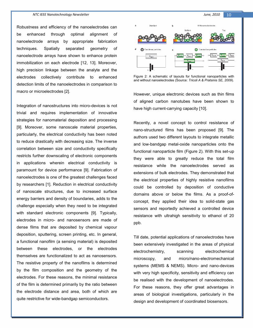
Figure 2: A schematic of layouts for functional nanoparticles with and without nanoelectrodes (Source: Tricoli A & Pratsinis SE, 2009).
However, unique electronic devices such as thin films
of aligned carbon nanotubes have been shown to
have high current-carrying capacity [10].
Recently, a novel concept to control resistance of
nano-structured films has been proposed [9]. The
authors used two different layouts to integrate metallic
and low-bandgap metal-oxide nanoparticles onto the
functional nanoparticle film (Figure 2). With this set-up
they were able to greatly reduce the total film
resistance while the nanoelectrodes served as
extensions of bulk electrodes. They demonstrated that
the electrical properties of highly resistive nanofilms
could be controlled by deposition of conductive
domains above or below the films. As a proof-of-
concept, they applied their idea to solid-state gas
sensors and reportedly achieved a controlled device
resistance with ultrahigh sensitivity to ethanol of 20
ppb.
Till date, potential applications of nanoelectrodes have
been extensively investigated in the areas of physical
electrochemistry, scanning electrochemical
microscopy, and micro/nano-electromechanical
systems (MEMS & NEMS). Micro- and nano-devices
with very high specificity, sensitivity and efficiency can
be realised with the development of nanoelectrodes.
For these reasons, they offer great advantages in
areas of biological investigations, particularly in the
design and development of coordinated biosensors.
11 NTC IEEE Nanotechnology Newsletter June, 2010
Future biomedical application of intelligent
nanosensors could facilitate a direct, point-of-care
clinical device enabling personalized medical care.
Innovative strategies to fabricate nanoelectrodes will
potentially open up other novel applications.
References
[1] D. W. M. Arrigan, “Nanoelectrodes, nanoelectrode arrays and
their applications”. Analyst, vol. 129, pp. 1157-1165, 2004.
[2] J. I. Yeh & H. Shi, “Nanoelectrodes for biological measurements”
Wiley Interdisciplinary Reviews: Nanomedicine and
Nanobiotechnology, 2010.
[3] R. M. Wightman & D. O. Wipf, “Voltammetry at
ultramicroelectrodes”. Electroanalytical Chemistry, ed. A. J. Bard,
Marcel Dekker, New York, pp. 15-267, 1989.
[4] A. M. Bond, “Past, present and future contributions of
microelectrodes to analytical studies employing voltammetric
detection: a review”, Analyst, vol. 119, pp. 1R-21R, 1994.
[5] R. J. Forster “Microelectrodes: new dimensions in
electrochemistry”, Chemistry Society Reviews, vol. 23, pp. 289-297,
1994.
[6] C. G. Zoski, “Ultramicroelectrodes: Design, Fabrication, and
Characterization”, Electroanalysis, vol. 14, pp. 1041-1051, 2002.
[7] R. Feeney & S.P. Kounaves, “On-site analysis of arsenic in
groundwater using a microfabricated gold ultramicroelectrode array”,
Electroanalysis, vol. 72, pp. 2222-2228, 2000.
[8] K. Stulik, C. Amatore, K. Holub, V. Maracek & W. Kutner,
“Microelectrodes. Definitions, characterization, and applications
(Technical report), Pure Applied. Chemistry, vol. 72, pp. 1483 -1492,
2000.
[9] A. Tricoli & S. E. Pratsinis, “Dispersed nanoelectrode devices”,
Nature Nanotechnology, vol. 5, pp. 54-60, 2010.
[10] S. J. Kang et al. “High-performance electronics using dense,
perfectly aligned arrays of single-walled carbon nanotubes”, Nature
Nanotech. vol. 2, pp. 230–236, 2007.
[11] G. D. Withey, J. H. Kim & J. Xu, “Wiring efficiency of a
metallizable DNA linker for site-addressable nanobioelectronic
assembly”, Nanotechnology, vol. 18, 424025, 2007.
[12] H. Shi & J. I. Yeh, “Part I: recent developments in
nanoelectrodes for biological measurements”, Nanomedicine, 2, pp.
587–598, 2007.
12 NTC IEEE Nanotechnology Newsletter June, 2010
Vision of Nanotechnology
NanoRobots
Manu Pallapa
Chongxiao Shen Mechatronics Engineering,
University of Waterloo.
Manu Pallapa
In 1959, Nobel prize winner Richard Feynman gave
the famous talk “There’s plenty of rooms at the bottom”
which inspired advances in nanotechnology.
Nanorobotics is an emerging field of nanotechnology
that may revolutionize the medical world in the future.
Developments in biosensors [17] and nano-kinetic
devices [18, 19] have significant impact in the
operation and locomotion of nanorobots. Here in this
article, the possibility of nanorobot teams working
together to assemble biomolecules for medical
purposes will be discussed.
Approach
Automation of atoms manipulation is one vital step
toward application usage of nanorobots in
nanomedicine. To manipulate molecules into special
patterns, the traditional approach of using Atomic
Force Microscopy (AFM) and Scanning Tunnelling
Microscopy (STM) require too much time and produce
imprecise work [3]. Cavalcanti et al. proposed the use
of artificial intelligence [4], fuzzy logic [5], neural
networks [6] and evolutionary techniques [7] to enable
automation of atom manipulation.
The concept of nanorobot teams performing coherent
work is theoretically possible with the development in
bio-computers [8] to carry out logical tasks, and the
progression in biosensors [8] and nanokinetic devices
[9] [10]. Possible issues related to quantum
mechanics, thermal motion and friction has been
addressed and resolved [11].
Figure 1: Virtual environment, top camera view (Source: Cavalvanti A. et al., 2005).
Applications
Multi-nanorobot teams can potentially perform various
medical tasks to process chemical reactions for injured
organs, or assist in chemotherapy to battle cancer [12].
Once the teams are equipped with nanosensors, they
can be employed to determine glucose demand, which
will benefit many diabetic patients [13].
Simulation environment
A computer simulated environment occupied by
nanorobots, biomolecules, obstacles and organ inlets
was investigated by Cavalcanti et al. (Figure 1). In
order to mimic a biological environment, the computer
simulation parameters were set to be under water,
where gravitational force is not considered, while
friction, adhesion and viscous forces dominate[14, 2].
13 NTC IEEE Nanotechnology Newsletter June, 2010
Figure 2: Sensor based navigational behaviour (Source: Cavalcanti A. et al., 2005).
Figure 3: Molecular Identification (Source: Cavalcanti A. et al., 2005).
Design of nanorobot
Mechanical parameters such as velocity, acceleration,
stoppage time, inertial force, viscous drag force,
rotational power, and turning angle all have to be
calculated and taken into consideration to design
robust nanorobots [3].
In the simulation program reported by Cavalcanti et al.,
the nanorobot was designed to capture molecules, and
assemble them. In order to mimick biological models,
the nanorobot was consisted of 3 main parts:
molecular sorting rotor, robot arm, and chemotactic
sensors used to identify different biomolecules [14].
The dimensions of the nanorobots used were 650 nm
in length, and 160 nm in diameter [3]. To avoid
adverse immune response, a diamondoid, artificial-
glycocalyx surface was chosen as the nanorobot
material [15]. A macroponder navigational system
assisted with beacons placed outside the human skin
may help in real-time identification of the nanorobot
location [15]. Implementation of acoustic
communication sensors provided an extended network
between nanorobot teams. This increased the
efficiency of work; however, too many messages sent
would result in inefficient energy consumption. One
possible alternative suggested in the study was the
use of oxygen and glucose which are abundant in the
human body [15].
Navigation was conducted using two counter-rotating
screw drives for propulsion, and the decision-making
was handled by sensors [15]. In a 3D world, the
nanorobots need to determine the shortest path
displacement while avoiding all obstacles. The
feedforward neural network model can help
accomplish this with low computational effort and high
accuracy [16].
Conclusion
Automating manipulation of atoms in nanomedicine
can be made possible by the proposed nanorobot.
However, from the simulation conducted by Cavalcanti
et al., there are many technical obstacles needing to
be address before nanorobots can be applied in the
real world such as identification of real time location,
and communication between nanorobots. Once these
barriers are taken down, the proposed integration of
medical engineering and medical science may
revolutionize the future of cancer research, and cure
severe maladies such as cancer using brand new
methods made possible with atom manipulation.
14 NTC IEEE Nanotechnology Newsletter June, 2010
References
[1] Weir N.A., Sierra D.P., and Jones J.F., “A review of research in
the field of nanorobotics”, Sandia report, Sandia National
Laboratories, SAND2005-6808, pp. 8 -9, 2005.
[2] R. A. Freitas Jr., “Nanomedicine, Volume I: Basic Capabilities”,
Landes Bioscience, 1999 R. A. Freitas Jr., “Nanomedicine, Volume
I: Biocompatibility”, Landes Bioscience, 2003.
[3] A. Cavalcanti, R. A. Freitas Jr., L. C. Kretly, “Nanorobotics control
design: A practical approach tutorial”, Robotics Today, SME, vol. 18,
no. 4, pp. 1-22, 2005.
[4] T. T Toth-Fejel, “Agents, assemblers, and ANTS: scheduling
assembly with market and biological software mechanisms”,
Nanotechnology, vol. 11, pp 133-137, 2000.
[5] V. Matellan, C. Fernandez, and J. M. Molina, “Genetic learning of
fuzzy reactive controllers”. Robotics and Autonomous Systems, vol.
25, pp. 33-41, 1998.
[6] H. D. Drucker, D.Wu, V. Vapnik, “Support vector machines for
spam categorization”, IEEE Transaction on Neural Networks, vol.
10, no. 5, pp. 1048-1054, 1999.
[7] J.J. Grefenstette, A. Schultz. “An evolutionary approach to
learning in robots”. Machine Learning Workshop on robot Learning,
New Brunswick, NJ, 1994.
[8] M. Hagiya. “From molecular computing to molecular
programming,” Proc. 6th DIMACS Workshop on DNA Based
Computers, Leiden, Netherlands, pp 198-204, 2000.
[9] J. Sun, M. Gao.,J. Feldmann, “Electric field directed layer by-
layer assembly of highly fluorescent CdTe nanoparticles,” Journal of
Nanoscience and Nanotechnology, vol. 1, no. 2, pp. 21-27, 2001.
[10] G. D. Bachand and C. D. Montemagno, “Constructing
organic/inorganic NEMS devices powered by biomolecular motors,”
Biomedical Microdevices, vol. 2, pp. 179-184, 2000.
[11] A. Hellemans, “German team creates new type of transistor-
like device,” News Analysis, IEEE Spectrum Magazine, pp. 20-21,
2003.
[12] M. N. V. R. Kumar, “Nano and microparticles as controlled drug
delivery devices”, J. Pharmacy Parmaceutical Science, vol. 3, no. 2,
pp. 234-258, 2000.
[13] E. Katz, A. Riklin, V. Heleg-Shabtai, I. Willner and A.
F.Bückmann, “Glucose oxidase electrodes via reconstitution of the
apo-enzyme: Tailoring of novel glucose biosensors”, Anal.Chim.
Acta., vol. 385, pp. 45-58, 1999.
[14] K. E. Drexler, “Nanosystems: molecular machinery,
manufacturing, and computation”, John Wiley & Sons, 1992.
[15] R. C. Merkle, “Nanotechnology and Medicine,” Advances in
AntiAging Medicine, Mary Ann Liebert Press, 1, pp. 277-286, 1996.
[16] M. T. Hagan, H. B. Demuth, and O. D. Jesús, “An introduction to
the use of neural networks in control systems,” International Journal
of Robust and Nonlinear Control, John Wiley & Sons, vol. 12, no. 11,
pp. 959-985, 2002.
[17] J. Sun, M. Gao, and J. Feldmann, “Electric Field Directed Layer-by-Layer Assembly of Highly Fluorescent CdTe Nanoparticles”, Journal of Nanoscience and Nanotechnology, vol. 1, no. 2, pp. 21-27, 2001.
[18] G. D. Bachand and C. D. Montemagno, “Constructing organic/inorganic NEMS devices powered by biomolecular motors”, Biomedical Microdevices, vol. 2, 179-184, 2000.
[19] R. Stracke, K. J. Böhm, J. Burgold, H. Schacht, and E. Unger, “Physical and Technical parameters determining the functioning of a knesin-based cell-free motor system”, Nanotechnology, vol. 11, pp. 52-56, 2000.
“For creative research on nanomaterials and nanotechnologies for electronic applications” “
Dr. Phaedon Avouris is an IBM Fellow and manager of Nanoscience & Nanotechnology at the T. J. Watson Research Center in Yorktown Heights, NY. He received his B.Sc. at the Aristotle University in Greece and his Ph.D. in Physical Chemistry at Michigan State University in 1974. He did postdoctoral work at UCLA and was a Research Fellow at AT&T Bell Laboratories before joining the staff of IBM’s Research Division at the Watson Research Center in 1978.
Over the years, he has worked in a wide range of research areas: laser spectroscopy, surface physics/chemistry, scanning tunneling microscopy, atom manipulation and nanoelectronics. His current research focuses on experimental and theoretical studies of the electronic and photonic properties of carbon-based nanostructures. The work also includes the design and study of nanoelectronic and optoelectronic devices based on these materials.
Dr. Avouris has published over 400 scientific papers. He has been elected Fellow of the American Academy of Arts and Sciences, the American Physical Society, the Institute of Physics of the U.K., the Academy of Athens (National Academy of Greece), the IBM Academy of Technology, American Association for the Advancement of Science, New York Academy of Sciences and the American Vacuum Society. He has received many awards including the APS Irving Langmuir Prize for Chemical Physics, the AVS Medard W. Welch Award for Surface Science, the Julius Springer Award for Applied Physics, the Richard E. Smalley Research Award of the Electrochemical Society, the Richard Feynman Nanotechnology Prize, the CNSI Nanoscience Prize and the IEEE John Raper Award. He has also received many IBM Corporation “Outstanding Technical Achievement” awards. He serves or served on the Editorial Boards of a number of journals and book series.
Dr. Ali Javey received a Ph.D. in chemistry from Stanford University in 2005, and served as a Junior Fellow of Harvard Society of Fellows from 2005 to 2006. He then joined the faculty of the University of California at Berkeley as an assistant professor of Electrical Engineering and Computer Sciences. Effective July 2010, he is promoted to an associate professor.
Professor Javey's research interests encompass the fields of chemistry and electrical engineering, focusing on the integration of synthetic nanomaterials for electronic, sensor and energy applications. His publications have been cited >4500 times with h index of 27. He has received a number of awards, including 2010 Alfred P. Sloan Fellowship, 2010 Mohr Davidow Ventures Innovators Award, 2009 National Academy of Sciences Award for Initiatives in Research, 2009 MIT Technology Review TR35, 2008 NSF CAREER Award, 2008 U.S. Frontiers of Engineering (National Academy of Engineering), and the 2003 Peter Verhofstadt Fellowship from the Semiconductor Research Corporation.
“For leadership excellence as Editor-in-Chief of IEEE Transactions on Nanotechnology”
Dr. Toshio Fukuda received the B.A. degree from Waseda University, Tokyo, Japan, in 1971, and the M.S and Dr. Eng. from the University of Tokyo, Tokyo, Japan, in 1973 and 1977, respectively. In 1977, he joined the National Mechanical Engineering Laboratory. In 1982, he joined the Science University of Tokyo, Japan, and then joined Nagoya University, Nagoya, Japan, in 1989. Currently, he is Director of Center for Micro-Nano Mechatronics and Professor of Department of Micro-Nano Systems Engineering at Nagoya University, where he is mainly involved in the research fields of intelligent robotic and mechatronic system, cellular robotic system, and micro- and nano-robotic system.
Dr. Fukuda was President of IEEE Robotics and Automation Society (1998-1999), Director of the IEEE Division X, Systems and Control (2001-2002), and Editor-in-Chief of IEEE / ASME Transactions on Mechatronics (2000-2002). He was President of IEEE Nanotechnology Council (2002-2003, 2005) and President of SOFT (Japan Society for Fuzzy Theory and Intelligent Informatics) (2003-2005). He was elected as a member of Science Council of Japan (2008-). He received the IEEE Eugene Mittelmann Award (1997), IEEE Millennium Medal (2000), IEEE Robotics and Automation Pioneer Award (2004), IEEE Robotics and Automation Society Distinguished Service Award (2005), Award from Ministry of Education and Science in Japan (2005). IEEE Nanotechnology Council Distinguished service award (2007). Best Googol Application paper awards from IEEE Trans. Automation Science and Engineering (2007). Best papers awards from RSJ (2004) and SICE (2007), Special Funai Award from JSME (2008), 2009 George Saridis Leadership Award in Robotics and Automation (2009), IEEE Robotics and Automation Technical Field Award (2010), IEEE Fellow (1995), SICE Fellow (1995), JSME Fellow (2001), RSJ Fellow (2004).
Aristides A. G. Requicha received the Engenheiro Electrotécnico degree from the Instituto Superior Técnico, Lisbon, Portugal, in 1962, and the Ph.D. in electrical engineering from the University of Rochester, Rochester, NY in 1970. He was a college and high school Valedictorian, and is listed as a highly cited author in the ISI Web of Science for 1980-99. He was awarded the Pioneer in Robotics and Automation Prize of the IEEE Robotics and Automation Society in 2008, the first-ever Pierre Bézier Prize of the Solid Modeling Association in 2007, and the Senior Research Award of the Viterbi School of Engineering of the University of Southern California (USC) in 2006.
Dr. Requicha holds the Gordon Marshall Chair in Engineering and is a Professor of Computer Science and Electrical Engineering at USC. He was the founding director of the Laboratory for Molecular Robotics at USC. His past research focused on geometric modeling of 3–D solid objects and spatial reasoning for intelligent engineering systems. His recent work is on robotic manipulation of nanometer-scale objects using scanning probe microscopes; nanorobot components and nanorobotic system integration; fabrication of nanostructures by robotic self-assembly; sensor/actuator networks; and applications in NEMS and nanobiotechnology. The long-term goals are to build, program, and deploy nanorobots and networks of nanoscale sensors/actuators for applications to the environment and health care.
He currently is the Editor-in-Chief of the IEEE Transactions on Nanotechnology, and recently stepped down as co-chair of the Micro/Nano Robotics and Automation Technical Committee of the IEEE Robotics and Automation Society. He is a member of the AAAI (Association for the Advancement of Artificial Intelligence), AVS (American Vacuum Society) and SME (Society of Manufacturing Engineers). He is a Fellow of the IEEE, of the ACM (Association for Computing Machinery) and of the AAAS (American Association for the Advancement of Science), and a member of Computer Graphics Pioneers and Sigma Xi.
“For pioneering and sustained contributions to compound semiconductor quantum structures and optoelectronic
devices”
Dr. Jagadish received the B.Sc. degree from Nagarjuna University, Guntur, India in 1977, the M.Sc(Tech) degree from Andhra University, Waltair, India in 1980 and the M.Phil. and Ph.D. degrees from the University of Delhi, India in 1982 and 1986, respectively. He was a Lecturer in Physics and Electronics at S.V. College, University of Delhi, during 1985-88 and worked at Queen’s University, Kingston, Canada, during 1988-90 as a post-doctoral research fellow. He moved to Australia in 1990 and established a major research program in the field of optoelectronics and nanotechnology. He is currently an Australian Laureate Fellow, Distinguished Professor and Head of Semiconductor Optoelectronics and Nanotechnology Group in the Department of Electronic Materials Engineering, Research School of Physical Sciences and Engineering, the Australian National University. His research interests include compound semiconductor optoelectronics and nanotechnology.
Jagadish is a winner of 2000 Institute of Electrical and Electronics Engineers, Inc (USA) (IEEE) Third Millennium Medal and a Distinguished Lecturer of IEEE Nanotechnology Council (NTC), IEEE Lasers and Electro-Optics Society (LEOS) and IEEE Electron Devices Society (EDS). He has published more than 580 research papers (390 journal papers), 5 US patents assigned, co-authored a book, co-edited a book and edited 12 conference proceedings. Jagadish has served as President of the IEEE Nanotechnology Council (2008 and 2009) and Associate Vice-President (Membership and Regional Activities- Asia-Pacific) of the IEEE Lasers and Electro-Optics Society (2008). He served as an elected member of EDS AdCom (1999-2004), and as Chair of Optoelectronic Devices Technical Committee of EDS (1998-2003) and Vice-President (Publications) of the IEEE Nanotechnology Council (2004-2005) and served as a member of the nanotechnology technical committee of EDS (2003-2005) and Chair of the NTC Nano-Optoelectronics, Nano-Optics and nano-photonics technical committee (2003-2006) and Chair of the NTC Awards Committee (2006-2008). He is a Fellow of the Institute of Electrical and Electronics Engineers, Inc. (USA), the American Physical Society, the Materials Research Society, the Optical Society of America, the Australian Institute of Physics, the Institute of Physics (UK), the Institute of Nanotechnology (UK), SPIE-the International Society for Optical Engineering, Electrochemical Society, the Institution of Engineering and Technology, American Association for Advancement of Science, American Vacuum Society, the Australian Academy of Technological Sciences and Engineering and the Australian Academy of Science. Jagadish served as an Associate Editor of the Journal of Nanoscience and Nanotechnology (2001-2005) and as an Associate Editor of the IEEE/OSA Journal of Lightwave Technology (2003-2008). He is currently serving as an Editor of the IEEE Electron Device Letters (2008-), an Editor of Progress in quantum Electronics (2008-) and an Editor of the Journal Semiconductor Technology and Science (2009-). He is a member of editorial boards of 12 journals. He is the Convener of the Australian Research Council Nanotechnology Network and ACT Node Director of the Australian National Fabrication Facility. He chaired many conferences (Program Chair of IEEE NANO2003, San Francisco, Co-Chair ICONN 2006, Brisbane, Co-Chair, IEEE NMDC 2006, 2008) and served on many international professional society committees. He advises high tech industries in Australia and overseas in the field of photonics and nanotechnology and collaborated with researchers from 20 different countries. He received Peter Baume Award (ANU's prestigious and highest award) for excellence in research and research leadership. He has also been awarded Australian Federation Fellowship (2004-2009) by the Australian Research Council and Distinguished Professor position (since 2009) by the Australian National University.
Submit on line at: http://ees.elsevier.com/nanocomnet/
Nano Communication Networks Journal is an international, archival and multi-disciplinary journal providing a publication vehicle for complete coverage of all topics of interest to those involved in all aspects of nano-scale networking and communications. Theoretical research contributions presenting new techniques, concepts, or analyses, applied contributions reporting on experiences and experiments, and tutorials are published.
Nano Communication Networks is a part of COMNET (Computer Networks) family of journals within Elsevier. The family of journals covers all aspects of networking except the nano-scale communications subject which is the target for this newly proposed journal.
1. Architectures and Systems for Nanocommunications
2. Novel Information Theory Aspects of Nanocommunications
3. Communication Protocols for Nanonetworks
4. Nano-addressing and Nano-coding for Communications
5. Molecular Communication aspects such as Ion Signaling, Molecular Motors, Flagellated Bacteria, Nanorods, Pheromones, Axons, Light Transducers, Capillaries
6. Quantum Theory and its Application on Nano-Communication Networks
7. Modeling and Simulation of Nano-Networks
8. Automata Models for Nanonetworks
9. Graph Theory Aspects of Nano-Networks
10. Nano-Sensor Networks: Architecture and Communication Protocols
11. Bio-nano Applications: Bio-micro/nanoelectronics, molecular scale chemical and biosensors, bio-MEMS technology, data and power management
12. Networks-on-Chip (NoC): Network architectures and topologies, NoC performance and trade-off analysis, Energy efficiency and power management, CAD flows for NoCs and MP-SoC platforms, Fault tolerance and reliability issues
13. Innovative System Interconnects: Nano-technologies and devices for on-chip interconnects (CNTs, semiconductor, metallic and DNA-templated nanowires), Molecular, optical and wireless interconnects, Interconnects for non-charge-based devices
14. Electro-Magnetic Communication for Nanonetworks (Nanoscale Electromagnetics, Carbon Nanotubes, Propagation models for nanoscale communications, planning and optimization, nano-radios, nano-batteries, nanoscale antennas, nano-arrays, EM aspects at nanoscale, reconfigurability issues)
The Eighteenth Annual International Conference on Composites/nano Engineering (ICCE - 18) Date: July 4–10, 2010 Venue: Alaska, USA More info: http://myweb.polyu.edu.hk/~mmktlau/ICCE/ICCE_Main.htm
SPIE NanoScience + Engineering symposium Date: August 1–5, 2010 Venue: California, USA More info: http://spie.org/nanoscience-engineering.xml
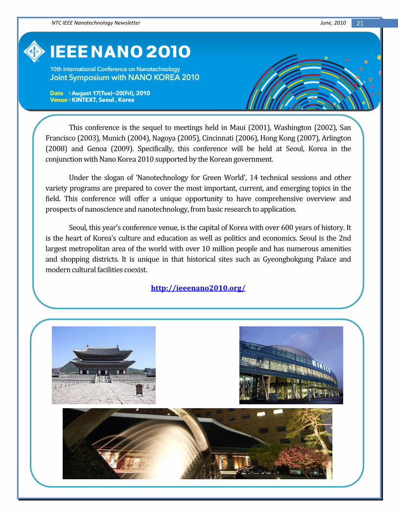
IEEE NANO 2010 Date: August 17–20, 2010 Venue: Seoul, Korea More info: http://ieeenano2010.org/
Third International NanoBio Conference 2010 Date: August 24–27, 2010 Venue: Zurich, Switzerland More info : http://www.nanobio.ethz.ch/ NMDC Nanotechnology Materials and Devices Conferences Date: October 12-15, 2010 Venue: Monteresy, California, USA More info: http://www.egr.msu.edu/nmdc2010/
IEEE Sensors 2010 Conference Date: November 1–4, 2010 Venue: Hawaii, USA More info: http://www.ieee-sensors2010.org/
International Conference on Solid-State and Integrated Circuit Technology Date: November 1–4, 2010 Venue: Shanghai, China
More info: http://www.icsict2010.com/index.htm
IEEE International Conference on Microelectronics (ICM) Date: December 19–22, 2010 Venue: Cairo, Egypt More info: http://www.ieee-icm.com/