16
INT. J. ELECTRONICS, 1998, VOL . 84, NO . 3, 187± 202 Numerical simulation of an optoelectronic thyristor in the regime of incomplete turn-o V. KOROBOV² , V. MITIN ² and W. BUCHWALD

INT J ELECTRONICS 1998 VOL 84 NO 3 187plusmn 202
Numerical simulation of an optoelectronic thyristor in the regime ofincomplete turn-o
V KOROBOVsup2 V MITINsup2 and W BUCHWALDsup3
Direct two-dimensional simulations are used to analyse the possibility ofcontrolling the carrier concentration in the gated base of a GaAs optoelectronicthyristor which operates in the regime of incomplete turn-o Modelling resultsindicate that the number of carriers light intensity current distribution and theposition of the light-emitting region the gated base of the thyristor can e ectivelybe changed using gate currents insu cient to turn the device completely o Theutilization of incomplete turn-o principle can be used for light-intensitymodulation and switching purposes
1 Introduction
Extensive research has been performed on III-V direct bandgap light-emittingthyristor-like PnpN structures (Simmons and Taylor l988 Crawford et al 1988Taylor and Cooke 1991 Kasahara et al 1988 Buchwald et al 1994 Heremanset al 1994) Work by numerous researchers shows that these devices have manyadvantages over traditional pn light-emitting diodes and lasers due to their compati-bility with key electrical elements of integrated circuits (Taylor and Cooke 1991) thecapability of generating noticeable optical output for a small optical or electricalinput (Simmons and Taylor 1988) and large-signal optical gain (Crawford et al1988) Optothyristors based on IIIplusmn V materials are currently used as e cient light-triggerable devices (Taylor and Cooke 1991) laser drivers (Buchwald et al 1994)elements of dynamic memories (Kasahara et al 1988) optical amplireg ers and opto-electronic switches (Heremans et al 1992) Conventional applications of light-emit-ting thyristor-like structures as optoelectronic switches are based on the transitionsbetween ON and OFF states These transitions can be triggered by optical or elec-trical signals It was suggested (Vagidov et al 1995) that a third intermediate state ofgate turn-o (GTO) thyristors may be interesting for an e ective gate control oflight-emitting thyristors In this intermediate state (named the regime of the incom-plete turn-o (Gribnikov et al 1996) gate currents are not su cient to turn thedevice o and the middle pn junction is partially reverse biased and partially for-ward biased For an appropriate value of the gate current Jg this heterogeneousthyristor state is stationary and stable The size of the central highly conductingregion depends on the applied gate current Negative gate currents can squeeze theelectronplusmn hole plasma If the anode current Ja is kept constant (ie if it is completelydetermined by the anode load resistance) we have the possibility of controlling thecurrent density in the center of the device the carrier concentrations the local light-emitting intensity and the total output power of radiation The utilization of gate
0020plusmn 721798 $1200 Ntilde 1998 Taylor amp Francis Ltd
Received 2 January 1997 accepted 2 June 1997sup2 Department of Electrical and Computer Engineering Wayne State University Detroit
MI 48202 USAsup3 US Army Research Laboratory Physical Sciences Directorate Fort Monmouth
NJ 07703 USA
squeezing in light-emitting structures may provide new methods of controlling theoptical output and essentially extend the functional capabilities of optothyristors bymaking direct modulation of the optical output independent of the carrier lifetime(Vagidov et al 1995) The gated turn-o mechanism was reg rst modelled by Wolley(Wolley 1966) His analytical description of turn-o was used as a guideline fordesign of GTO power thristors (Kurata et al 1982 Azuma and Kurata 1988)Gribnikov and Rothwarf (1994) and Dutta and Rothwarf (1992) focused on theanalytical calculation of storage and fall times when a negative voltage pulse su -cient to switch the device completely o is applied to the gate terminal A steady-state theory for the potential distribution and current densities in the incomplete turno regime has been developed (Vagidov et al 1995 Gribnikov et al 1996) whichutilizes linear recombination mechanisms for the case of low base injection levelsThis analytical approach assumes that the thyristor structure is inreg nitely long in thedirection perpendicular to the current macr ow and thus a quasi-one dimensionalapproximation holds Analysis of the two-dimensional carrier distribution at highinjection levels and arbitrary gate signals has not yet been carried out Because ananalytical approach has several natural limitations it is interesting to obtain aninsight into the device operation in the incomplete turn-o mode using directnumerical modelling
The goal of this paper is to present the results of exact two-dimensional simula-tions of a GTO thyristor which operates in the regime of incomplete turn-o Although signireg cant work has been presented on thyristor-like optical switchespractically nothing exists on computer simulations of such devices where an accu-rate physical model could play an important role in design and optimization Todate most work has been done on the computer simulation of silicon power thyr-istors (Cornu and Lietz 1972 Herlet 1968 Kurata 1976 Adler 1978) Other research(Fardi 1994 1996 Carson et al 1989 1991 Korobov and Mitin 1996) deals with thenumerical simulation of IIIplusmn V PnpN optical switches The numerical approachdeveloped by Fardi (1994 1996) accounts for several important physical e ectssuch as band-gap discontinuity avalanche breakdown and optical carrier genera-tion This approach also has current boundary conditions which are more suitablefor four-layer PnpN device where terminal currents are single-valued in voltage for agiven current under any circumstances This model was successfully used for ananalysis of steady-state currentplusmn voltage characteristics in IIIplusmn V PnpN switchesand transient simulations were reported by Carson et al (1991) and Korobov andMitin (1996) Note that almost all the models cited above are one-dimensional andthe current squeezing e ect is essentially a two-dimensional phenomenon To eval-uate the e ects of applied gate voltage on steady-state and transient characteristics ofgate-controlled optothyristors we have created a two-dimensional solver which maybe useful for the analysis and optimization of multi-terminal thyristor-like devicesoperating in the regime of incomplete turn-o
2 Numerical approach
The semiconductor device equations that we solve are Poissonrsquos equation forelectrostatic potential y
F1( x ) = Ntilde middotsup2 Ntilde y - q(n - p + NA - ND) = 0 (1)
188 V Korobov et al
and time-dependent current continuity equations for electron and hole concentra-tions n and p
F2( x ) = para npara t - Ntilde middotJn
q+ R(np) - G = 0 (2)
F3( x ) = para ppara t
+ Ntilde middotJp
q+ R(np) - G = 0 (3)
Here Jn and Jp are electron and hole current densities NA and ND are donor andacceptor concentrations q is the electron charge and G is the rate of optical genera-tion x is a group of variables consisting of n p and y The recombination termin (2) and (3) accounts for three major mechanisms of generationplusmn recombinationband-to-band radiative recombination Rsp Hallplusmn Shockleyplusmn Read RHSR and AugerRAug terms
R(np) = Rsp + RHSR + RAug (4)
Rsp = B0(np - n2i ) (5)
RHSR =np - n2
iiquest1(n + n1) + iquest2( p + p1)
(6)
RAug = (C1n + C2 p)(np - n2i ) (7)
Material parameters correspond to GaAs ni stands for the intrinsic carrier concen-tration in GaAs B0 = 77 acute 10- 10 cm3 s is the spontaneous recombination coe -cient The parameters of the HSR recombination are iquestn = iquestp = 5 acute 10- 7 s andn1 = p1 = ni the intrinsic concentration Rsp gives the main contribution to thetotal recombination term R(n p) in (4) The impact ionization mechanism is notincluded in the current simulator because as will be seen from our results this e ectis not important in the range of applied voltages under considerations The tempera-ture is assumed to be 300K
The box integration method (Selberherr 1984) has been used to discretizePoissonrsquos equation A Scharfetterplusmn Gummel scheme (Scharfetter and Gummel1969) has been implemented for the dicretization of the drift-di usion continuityequations A fully implicit reg nite di erence scheme generates a nonlinear system ofdiscrete equations
F( x ) = 0 (8)
where F is a vector composed of the discretized forms of these three equations for allthe grid points and x is a vector form of n p and y for the entire grid structure Thissystem of nonlinear equations has been solved by the Newtonplusmn Raphson method(Selberherr 1984) After linearization we obtain
para F1 para y para F1 para n para F1 para ppara F2 para y para F2 para n para F2 para p
para F3 para y para F3 para n para F3 para p
aeligccedilegrave
oumldivideoslashmiddot
D yD nD p
aeligccedilegrave
oumldivideoslash=
- F1
- F2
- F3
aeligccedilegrave
oumldivideoslashor in short notations
FAcirc ( x (m- 1) ) D x (m) = - F( x (m- 1) ) (9)
Optoelectronic thyristor in the regime of incomplete turn-o 189
where FAcirc is the jacobian matrix of F and x m- 1 is the vector form of the solution fromthe previous (m - 1)th iteration and D x m is the increment of x at the mth Newtoniteration The Yale Sparse Matrix Solver (Eisenstat et al 1977) has been used for theinversion of the jacobian matrix at each iteration step
3 Results and discussions
Figure 1 shows the geometry of the simulated PnpN gate turn-o thyristor(GTO) The simulated device is a rectangular structure where two outer emitterregions of 3 m m width (P and N) have doping concentrations 1017 cm- 3 The n-and p-bases are doped with 1015 cm- 3 and have widths 10 m m and 4 m m respectivelyThe sizes of the gate and cathode electrodes are 3 m m and 12 m m The device length inthe direction perpendicular to the current macr ow is 40 m m
31 ON stateGenerally a thyristor exhibits a current-controlled type of switching character-
istic The static thyristor voltage is uniquely dereg ned as a single-valued function of thecurrent which is not the case if the thyristor current is viewed as a function of thevoltage In general there are three currents that correspond to a given voltage one in
190 V Korobov et al
Figure 1 The geometry of the simulated thyristor
the forward blocking branch the second in the holding branch and the third in theconduction branch Thus in a purely theoretical sense it is unknown which of theoperating conditions is reached as a consequence of the numerical convergence Inthe regime with reg xed electrode current the currentplusmn voltage characteristic is a single-valued function of the current The inclusion of current boundary conditionsrequires the integration of current density along a contact Discretizing this formof boundary condition introduces far neighbour interactions which destroy thepentadiagonal nature of the jacobian and often complicates the solution of the set oflinear equations due to the convergency problems (Adler et al 1987) In practice thisfact imposes strict limitations on the magnitudes of current increments if the solu-tion at the previous bias is used as an initial guess for the next bias It has beenshown (Kurata 1976) that if the initial trial conditions are close to the true solutionfor the ON state this solution can be obtained using the voltage-controlled type ofboundary conditions A similar argument holds for the forward blocking state In aone-dimensional problem Kurata (1976) used an analogy between thyristors in thereg red state and p-i-n rectireg ers to reach an upper branch of the Iplusmn V characteristics
In the two-dimensional problem to reach the ON state solution we proceed asfollows After obtaining the solution for the zero bias we then decrease the cathodevoltage at a reg xed anode and gate potential The anode is assumed to be groundedand the gate potential is kept equal to its built-in potential The decrease of thecathode voltage means that the gate e ectively becomes positive with respect tocathode and thus positive gate current increases the carrier concentrations in thep-base The excess carriers provide the biasing action which cause a decrease ofpotential barrier of the middle junction and the thyristor turns on Next we reg xthe cathode potential and total anode current Now currents through the gate elec-trodes can be changed and we can study the e ects of gate current on carrier andpotential distributions This procedure was found to be useful for the reduction ofthe total computational time Figure 2(a) shows the carrier distributions along thecentre of the device for the anode current Ia = 028Acm and no gate currents Theelectron n(xy) and hole p(xy) concentrations are found to be nearly uniform andalmost equal to each other in both bases (ie n(xy) p(xy) 3 acute 1016 cm- 3 at3 m mlty lt17 m m) and much greater than the background doping concentrations(1015 cm- 3) From Fig 2(b) one can see that potential barrier across the middle pnjunction practically disappears due to high injection level in both bases
32 Gate squeezing e ectsThe application of a negative gate bias causes the removal of excess holes
through the gate contact The removal of holes is accompanied by a removal ofelectrons to maintain space charge neutrality Because the removal of one type ofcarrier is always balanced by the removal of a carrier of the opposite type followingWolley (1966) we concern ourselves with only one type of excess carrier which in thiscase we choose to be electrons Fig 3 shows the electron concentration for the gatecurrent Ig = 0028Acm which corresponds to a gate potential of - 42V It is seenthat in the regions adjacent to the gates the electron concentration decreases dras-tically Analysis of the hole distribution shows a concentration that is equal to theequilibrium value of p = 1015 cm- 3 in these regions The number of holes startsdecreasing in the n-side of the middle pn junction at y = 13 m m It is clear fromFig 2 that in the p-base excess holes and electrons are present only in the central
Optoelectronic thyristor in the regime of incomplete turn-o 191
192 V Korobov et al
(a)
(b)
Figure 2 (a) Electron and hole concentrations in the ON state along the centre of the devicewith anode current Ia = 028Acm and no gate currents in the inner regions at3 m m lty lt17 m m carrier concentrations are very close to each other (n p 3 acute 1016 cm- 3) curves 1 and 2 correspond to electron and hole densities Thedashed line 3 shows equilibrium electron distribution (b) Electrostatic potential dis-tribution for the same anode current there is no potential barrier across the middle pnjunction
part of the device Due to carrier removal portions of the middle pn-junction JMcome from saturation and depletion regions with high electric reg elds (see Fig 4) areformed near the gates As can be seen in Fig 5 these regions are low-conducting andthey block the current
The driven decrease of carrier concentrations in the p-base makes the cathode-p-base junction also partially reverse biased Fig 5 shows that the current density atthe cathode-p-base junction is squeezed and electrons are injected only from thecentral part of the cathode From Fig 3 it is clearly seen that there is a heterogeneousstate of carrier distribution inside the thyristor with two substantially di erentregions of high and low concentrations The transition layer between regions isrelatively thin thus the carrier squeezing e ect is well pronounced From theabove it is obvious that light emission due to spontaneous recombination in thep-base would be concentrated in the centre of the device and would be negligible inthe depletion regions Fig 6 shows the distribution of the spontaneous recom-bination rate calculated using (5) in the controlling p-base There is a sharp maxi-mum at the centre of the device where excess carriers are present The number ofemitted photons from the central part of the device is many orders of magnitudegreater than the radiation from the unsqueezed region This well pronounced squeez-ing e ect gives us a hope that an experiment to demonstrate the proof of principlebehind PnpN structures operating in an incomplete turn o mode can be successfulLight from the unsqueezed portion of the devices probably will not substantiallylimit the ability to detect the modulated optical signal due to the applied gatecurrents
Optoelectronic thyristor in the regime of incomplete turn-o 193
Figure 3 Electron concentration plot in the regime of optothyristor incomplete turn-o distribution corresponds to the anode current Ia = 028Acm and two equal gate cur-rents Jg1 = Jg2 = 0028Acm JM indicates the location of the middle pn junction
194 V Korobov et al
Figure 4 Electric reg eld distribution for the same currents as in Fig 3 areas of high electricreg eld correspond to the reverse biased middle p-n junction the central part of thejunction is still forward-biased
Figure 5 Lateral component of current density J in the thyristor incomplete turn o regimetotal gate and anode currents are the same as in Fig 3 the current is squeezed towardsthe centre of the device and macr ows in the regions where the middle and cathode-p-basejunctions are forward-biased
The distributions in Figs 3plusmn 6 were plotted for the ratio of currents Ia Jg = 10Thus the gate current which is only 10 of the anode current causes this dramaticinhomogeneous carrier distribution
Our analysis has shown that a well-pronounced squeezing e ect depends on themagnitude of the anode current and geometrical device parameters If the anodecurrent is too small the device will be turned o before the central conductingchannel is formed For the simulated structure it was impossible to obtain essentiallyinhomogeneous carrier distributions if the anode current was less than 005Acm Atthese anode currents a gate voltage changed the carrier distribution but regions withsmall and large concentrations separated by a narrow boundary did not appearInstead the voltage drop across the device increased sharply and the device wasturned completely o At high anode currents there is another limitation tothe applied gate signal At a high negative gate bias the regions of high electricreg eld at the edges of the middle pn-junction become wide enough to reach the gateelectrode In this case the size of the conducting channel in the p-base cannot becontrolled Making the p-base wider is not desirable because then higher gate cur-rents are required to squeeze the electronplusmn hole plasma However a higher doping ofthe p-base would solve this problem It was also found that the width of the n-base isvery important in controlling the size of the conducting region with a small gatesignal In the structure presented here the hole current is concentrated in the centreof the device If some fraction of the injected holes reaches the region of the reversebiased middle pn junction they will be carried to the gates by the strong electricreg eld of the depletion region These holes contribute to the parasitic gate currentmacr owing through the Pnp transistor This current is not related to the squeezing of
Optoelectronic thyristor in the regime of incomplete turn-o 195
Figure 6 Rate of spontaneous recombination in the controlling p-base for the same anodeand gate currents as in Fig 3
the conducting region and decreases the sensitivity with respect to the gate control Itwas found that if we decreased the width of the n-base by a factor of two and keptthe same initial excess carrier concentrations then the gate current required toachieve the same size of the conducting channel as in Figs 3plusmn 6 was even higherthan the device total anode current
For the structure presented here an increase of current density in the centre of thedevice was accompanied by an increase in the anodeplusmn cathode voltage drop Thecarrier concentration in the conducting region was found to monotonically decreasewith an increase of the negative gate voltage An increase in the carrier concentrationby up to 10 due to the current squeezing in comparison with the zero gate signalcase was found in the wider structure with a device cross-section of 100 acute 200 m mFor this wider structure during the initial stage of gate turn-o the carrier concen-tration was found to increase slightly in the centre of the device and then decrease ina fashion similar to the narrower device
At gate currents greater than 003Acm the supply of holes into the plasmaregion is no longer su cient to sustain a macr ow of electrons across the p-base ForJg gt0035Acm the anode voltage drop increases rapidly and a potentialbarrier develops across the whole area of the middle p-n junction This means thatthe critical gate current Jcr
g which determines the upper boundary of the incompleteturn-o regime (Wolley 1966) for the simulated structure is approximatelyJcr
g = 0035Acm The electric reg eld distribution for Jg = 004Acm is plotted inFig 7 Regions of high electric reg eld reached each other and the whole middle pnjunction is reverse-biased The carrier concentration at a given gate current
196 V Korobov et al
Figure 7 Electric reg eld distribution for anode current Ia = 028Acm and gate currents Jg =004Acm the whole middle pn junction is reverse-biased
Optoelectronic thyristor in the regime of incomplete turn-o 197
(a)
(b)
Figure 8 Shift of electron density distribution due to the di erent gate currents (a) ratio ofcurrents Jg2 Jg1 = 263 (b) Gate current ratio is Jg1 Jg2 = 263
decreases almost up to the equilibrium values Thus the conducting regions shrinksto a very narrow reg lament and the device turns o
33 Shift of the conducting channelWe have considered the case where equal currents macr owing through each gate
control the size of the conduction region Dual gates make it possible to control theposition of the light-emitting region This control can be used for a new type ofoptical space division switches The major component of the switches is a device thatcan direct light in one of several directions in reaction to an external control (Lu et al1995 Yao and OrsquoMahony 1994 Kalman et al 1992)
To study the possibility of the conducting channel shift we have simulated theGTO thyristor with di erent gate currents Jg1 and Jg2 macr owing through the left andright gates Results are presented for the ratios Jg1 Jg2 = 038 and Jg1 Jg2 = 263The total gate current Jg = Jg1 + Jg2 was constant for both cases and was equal toJg = 005Acm Figs 8(a) and 8(b) indicate that for these gate current ratios theconducting region can be shifted to one or the other edge of the cathode withoutchanges in the width of the conducting channel It is seen that the region of highcarrier concentrations is located closer to the gate with the smaller current The shiftof the blocking regions causes a shift in the position of the maximum total currentdensity and of the maximum of carrier concentrations The spontaneous recombina-tion rate given by (5) is shown in Fig 9 for the gated base Two maxima correspondto the same gate currents ratios as in Fig 8 From the distribution of the sponta-neous recombination rate shown in Fig 9 it is possible to conclude that the shift of
198 V Korobov et al
Figure 9 Two plots of spontaneous recombination rate calculated for carrier distributionsshown in Figs 8(a) and (b)
Optoelectronic thyristor in the regime of incomplete turn-o 199
(a)
(b)
Figure 10 Results of transient simulation when the gate current ratio Jg1 Jg2 was changedfrom 263 to 038 (a) electron current distribution at t = 0 (b) electron current densityat t = 05ns
light intensity across the p-base is greater than a half-width of the channel regionwhen gate currents were equal to zero and is approximately equal to the wholelength of the cathode (12 m m)
We have also performed transient simulations where gate current ramps wereapplied to the gates The initial carrier distribution corresponds to Fig 8(a) At t = 0the gate currents have been changed so that their ratio became 263 Simulationresults show that it takes approximately 05ns for the electron distribution to coin-cide with the plot of Fig 8(b) The distribution of the electron current density att = 05ns is shown in Fig 10(b) Although the transient process did not reg nish at thistime carrier concentrations demonstrate a well-dereg ned maximum very similar tothat in Fig 8(b) at the right edge of the anode Thus the shift of the conductingregion over a distances nearly 12 m m occurs during 05ns It is easy to estimate thatchannel shifts over distances comparable with the GaAs radiation wavelength maybe made during time intervals of order 01ns This fact may lead to a new design offast optoelectronic devices where optical switching could be based on the shift of thelight-emitting region
4 Conclusion
We have performed exact two-dimensional simulations of a GaAs GTO light-emitting thyristor which operates in the regime of incomplete turn-o Simulationresults show that relatively small gate currents can create inhomogeneous currentand carrier distributions and thus make possible e ective gate control of lightemission in optoelectronic thyristors The size of the conducting region was foundto be a sensitive function of applied gate current which squeezes the electronplusmn holeplasma towards the centre of the device Small gate currents change the rate ofspontaneous recombination by many orders of magnitude in a large area of thedevice This can be used for light-intensity modulation in light-emitting devices aswell as in optical switching applications The device can be further optimized by theaddition of heterojunctions for the conreg nement of light or a Fabryplusmn Perot cavity forlazing
We have demonstrated numerically the possibility of shifting the current-con-ducting region in the case of asymmetric gate currents In our simulation this shiftwas found to be at least 12 m m which is larger than the width of the conducting light-emitting region Shifts of the emitting region can be used to create a new type of logicoptothyristors or memory cell Simulation results show that switching times in thesubnanosecond range can be obtained in this type of device
ACKNOWLEDGMENT
This work was supported by the NSF
References
Adler M S 1978 Accurate calculations of the forward drop and power dissipation inthyristors IEEE Transactions on Electron Devices 25 16plusmn 22
Adler M S Pattnayak D N Baliga B J Temple V K and Chang H R 1987Device physics and modelling of integrated power devices Proceedings of the FifthInternational Conference on the Numerical Analysis of Semiconductor Devices andIntegrated-Circuits pp 1plusmn 19
200 V Korobov et al
Azuma M and Kurata M 1988 GTO thyristors Proceedings of the IEEE 76 419plusmn427
BuchwaldW RZhao J HZhuLSchauer Sand Jones KA 1994 A three terminalInPInGaAsP optoelectronic thyristor IEEE Transactions on Electron Devices 41620plusmn 622
Carson R F Hughes R C ZipperianT EWeaver HT BrennanT M HammonsB E and Klem J F 1989 Radiation responce of optically-triggered GaAs thyris-tors IEEE Transactions on Nuclear Science 36 2147plusmn 2154
Carson R F Hughes R C and Weaver H T 1991 Long switching delay mechanismsfor optically triggered GaAs thyristors Applied Physics Letters 59 834plusmn 836
Cornu J and Lietz M 1972 Numerical investigation of the thyristor forward character-istic IEEE Transactions on Electron Devices 19 975plusmn 981
Crawford W Taylor G Cooke P Chang T Y Tell B and Simmons J 1988Optoelectronic transient response of the self-aligned double heterostructure optoelec-tronic switch Applied Physics Letters 53 1797plusmn 1799
Dutta R and Rothwarf A 1992 A new analytical model for gated turn-o of thyristorsIEEE Transactions on Electron Devices 39 1752plusmn 1757
Eisenstat S C Gursky M C Schultz M H and Scherman A N 1977 The Yalesparse matrix package 2 The nonsymmetric codes Technical report 114 YaleUniversity
Fardi H Z 1994 Simulation and modelling of p-n-p-n optical switches IEEE Trans-actions on Computer-Aided Design of Integrated Circuits and Systems 12 666plusmn 6711996 E ects of interface and bulk recombination on switching characteristics ofAlGaAsGaAs pnpn bistable device IEEE Transactions on Electron Devices 422248plusmn 2250
Gribnikov Z and Rothwarf A 1994 A new intermediate state model for the GTOrelation to the turn-o process Solid-state Electronics 37 135plusmn 139
Gribnikov Z S Korshak A N Vagidov N Z and Mitin V V 1996 E ect of baseparameters on gate-controlled squeeze of current-conducting region in pnpn struc-tures Solid-state Electronics 39 915plusmn 922
Heremans P L Kuijk M and Borghs G 1992 Fast turn-o of two-terminal double-heterojunction optical thyristor Applied Physics Letters 61 1326plusmn 1328
Heremans P Kuijk MVounckx R and Borghs G 1994 Properties and applicationsof optical thyristors Journal de Physique 4 2391plusmn 2404
Herlet A 1968 The forward characteristics of silicon power rectireg ers at high currentdensities Solid-state Electronics 11 717-742
Kalman R F Kazovsky L G and Goodman JW 1992 Space division switches basedon semiconductor optical amplireg ers IEEE Photonics Technology Letters 4 1048-1049
Kasahara KTashiroY Namao N Sugimoto M andYanaseT 1988 Double hetero-structure optoelectronic switch as a dynamic memory with low-power consumptionApplied Physics Letters 52 679plusmn 681
Korobov V and Mitin V 1996 Reverse recovery of a GaAs optoelectronic thyristorJournal of Applied Physics 79 1143-1150
Kurata M 1976 One-dimensional calculation of thyristor forward voltages and holdingcurrents Solid-state Electronics 16 681plusmn 688
Kurata M Azuma M Ohashi HTakigami K Nakagawa A and Kishi K 1982Gate turn-o thyristors Semiconductor Devices for Power Conditioning (New YorkPlenum) pp 91plusmn 119
Lu Y-C Cheng J Zolper J C and Klem J 1995 Integrated opticaloptoelectronicswitch for parallel optical interconnects Electronics Letters 31 579plusmn 580
Scharfetter D L and Gummel H K 1969 Large-signal analysis of a silicon Read diodeoscillator IEEE Transactions on Electron Devices 16 64plusmn 77
Selberherr S 1984 Analysis and Simululation of Semiconductor Devices (New YorkSpringer-Verlag)
Simmons J and Taylor G 1988 Electronic conduction and generation mechanism in thedouble heterostructure optoelectronic switch (DOES) IEEE Trancsactions on ElectronDevices 35 1278plusmn 1284
Optoelectronic thyristor in the regime of incomplete turn-o 201
Taylor G and Cooke P 1991 Determination of the switching condition in the quantum-well double-heterostructure optoelectronic switch (DOES) IEEE Transactions onElectron Devices 39 2529plusmn 2541
Vagidov N Z Gribnikov Z S Korshak A N and MitinVV 1995 Intermediate stateof a controllable four-layer p-n-p-n structure Semiconductors 29 1021-1029
Wolley E 1966 Turn-o in pnpn devices IEEE Transactions on Electron Devices 13 590plusmn597
Yao J and OrsquoMahony M J 1994 Experimental study of semiconductor laser amplireg ers forphotonic time and space switching amplireg ers International Journal of Optoelectronics9 219plusmn 220
202 Optoelectronic thyristor in the regime of incomplete turn-o
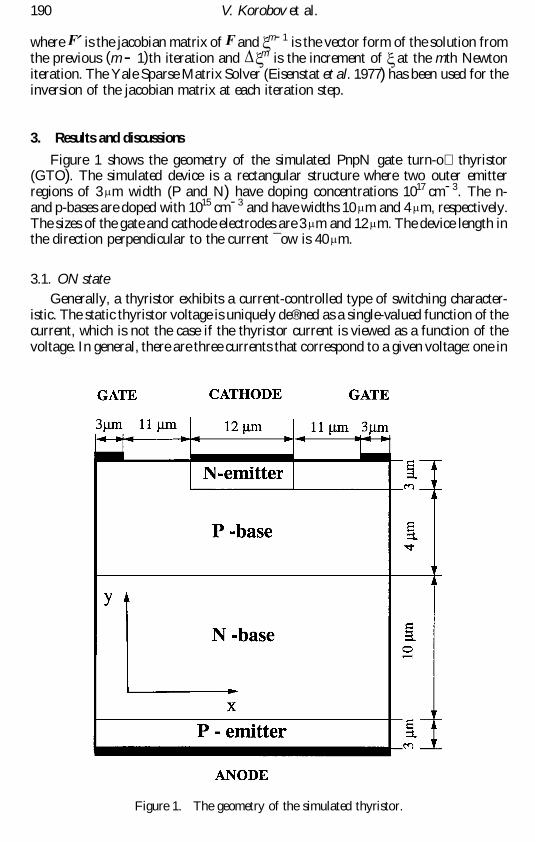
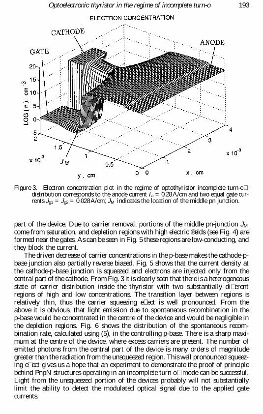
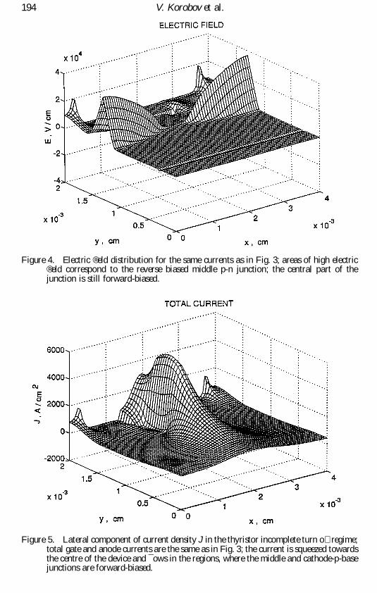
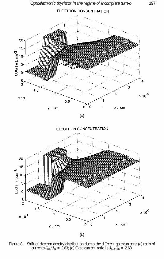
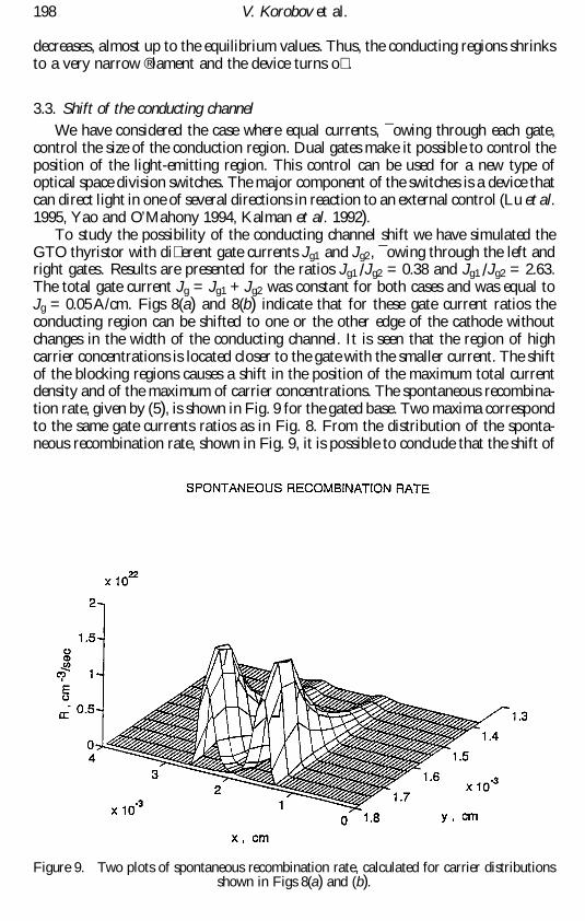
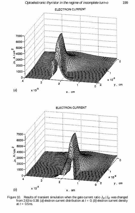


