319942-02 December 2008 Numonyx™ StrataFlash ® Embedded Memory (J3-65nm) 256-Mbit Datasheet Product Features Architecture — Multi-Level Cell Technology: Highest Density at Lowest Cost — 256 symmetrically-sized blocks of 128 Kbytes Performance — 95 ns initial access time for Easy BGA — 105 ns initial accsss time for TSOP — 25 ns 16-word Asynchronous page-mode reads — 512-Word Buffer Programming at 1.46MByte/s (Typ) Voltage and Power —V CC (Core) = 2.7 V to 3.6 V —V CCQ (I/O) = 2.7 V to 3.6 V — Standby Current: 65 μA (Typ) — Erase & Program Current: 35 mA (Typ) — Page Read: 12 mA (Typ) Quality and Reliability — Operating temperature: -40 °C to +85 °C — 100K Minimum erase cycles per block — 65 nm Numonyx TM ETOX™ X Process technology Security — Enhanced security options for code protection — Absolute protection with V PEN = GND — Individual block locking — Block erase/program lockout during power transition — Password Access feature — One-Time Programmable Register: 64 OTP bits, programmed with unique information by Numonyx 64 OTP bits, available for customer programming Software — 20 μs (Typ) program suspend — 20 μs (Typ) erase suspend — Numonyx™ Flash Data Integrator (FDI) — Common Flash Interface (CFI) Compatible Packaging — 56-Lead TSOP — 64-Ball Easy BGA package
Density at Lowest Cost— 256 symmetrically-sized blocks of 128
KbytesPerformance— 95 ns initial access time for Easy BGA— 105 ns initial accsss time for TSOP— 25 ns 16-word Asynchronous page-mode
reads— 512-Word Buffer Programming at
1.46MByte/s (Typ) Voltage and Power— VCC (Core) = 2.7 V to 3.6 V— VCCQ (I/O) = 2.7 V to 3.6 V— Standby Current: 65 µA (Typ) — Erase & Program Current: 35 mA (Typ)— Page Read: 12 mA (Typ)Quality and Reliability— Operating temperature:
-40 °C to +85 °C— 100K Minimum erase cycles per block— 65 nm NumonyxTM ETOX™ X Process
technology
Security— Enhanced security options for code
protection— Absolute protection with VPEN = GND— Individual block locking— Block erase/program lockout during power
64 OTP bits, programmed with unique information by Numonyx64 OTP bits, available for customer programming
Software— 20 µs (Typ) program suspend— 20 µs (Typ) erase suspend— Numonyx™ Flash Data Integrator (FDI)— Common Flash Interface (CFI) CompatiblePackaging— 56-Lead TSOP — 64-Ball Easy BGA package
Datasheet December 20082 319942-02
Legal Lines and DisclaimersINFORMATION IN THIS DOCUMENT IS PROVIDED IN CONNECTION WITH NUMONYX™ PRODUCTS. NO LICENSE, EXPRESS OR IMPLIED, BY ESTOPPEL OR OTHERWISE, TO ANY INTELLECTUAL PROPERTY RIGHTS IS GRANTED BY THIS DOCUMENT. EXCEPT AS PROVIDED IN NUMONYX'S TERMS AND CONDITIONS OF SALE FOR SUCH PRODUCTS, NUMONYX ASSUMES NO LIABILITY WHATSOEVER, AND NUMONYX DISCLAIMS ANY EXPRESS OR IMPLIED WARRANTY, RELATING TO SALE AND/OR USE OF NUMONYX PRODUCTS INCLUDING LIABILITY OR WARRANTIES RELATING TO FITNESS FOR A PARTICULAR PURPOSE, MERCHANTABILITY, OR INFRINGEMENT OF ANY PATENT, COPYRIGHT OR OTHER INTELLECTUAL PROPERTY RIGHT. Numonyx products are not intended for use in medical, life saving, life sustaining, critical control or safety systems, or in nuclear facility applications.
Numonyx B.V. may make changes to specifications and product descriptions at any time, without notice.
Numonyx B.V. may have patents or pending patent applications, trademarks, copyrights, or other intellectual property rights that relate to the presented subject matter. The furnishing of documents and other materials and information does not provide any license, express or implied, by estoppel or otherwise, to any such patents, trademarks, copyrights, or other intellectual property rights.
Designers must not rely on the absence or characteristics of any features or instructions marked “reserved” or “undefined.” Numonyx reserves these for future definition and shall have no responsibility whatsoever for conflicts or incompatibilities arising from future changes to them.
Contact your local Numonyx sales office or your distributor to obtain the latest specifications and before placing your product order.
Copies of documents which have an order number and are referenced in this document, or other Numonyx literature may be obtained by visiting the Numonyx website at http://www.numonyx.com.
Numonyx, the Numonyx logo, and StrataFlash are trademarks or registered trademarks of Numonyx B.V. or its subsidiaries in other countries.
*Other names and brands may be claimed as the property of others.
11.0 Registers ................................................................................................................. 3011.1 Status Register ................................................................................................. 3011.2 Status Signal .................................................................................................... 3111.3 OTP Protection Register...................................................................................... 32
12.0 Power and Reset Specifications ............................................................................... 3512.1 Power-Up and Power-Down................................................................................. 35
Numonyx™ StrataFlash® Embedded Memory (J3-65nm)
Datasheet December 20084 319942-02
12.2 Reset Specifications ...........................................................................................3612.3 Power Supply Decoupling....................................................................................37
13.0 Maximum Ratings and Operating Conditions ............................................................3813.1 Absolute Maximum Ratings .................................................................................3813.2 Operating Conditions..........................................................................................38
14.0 Electrical characteristics ..........................................................................................3914.1 DC Current Specifications ...................................................................................3914.2 DC Voltage Specifications....................................................................................4014.3 Capacitance .....................................................................................................40
15.0 AC characteristics ....................................................................................................4115.1 AC Test Conditions.............................................................................................4115.2 AC Read Specifications .......................................................................................4315.3 AC Write Specification ........................................................................................46
16.0 Program and erase characteristics ...........................................................................4816.1 Program & Erase Specifications............................................................................48
A Reference Information.............................................................................................50A.1 Common Flash Interface.....................................................................................50A.2 Query Structure Output ......................................................................................50A.3 Flow Charts.......................................................................................................57
B Terms, definitions, and acronyms ............................................................................62B.1 Nomenclature....................................................................................................62B.2 Acronyms .........................................................................................................62B.3 Conventions......................................................................................................63
C Revision History.......................................................................................................64
December 2008 Datasheet319942-02 5
Numonyx™ StrataFlash® Embedded Memory (J3-65nm)
1.0 Functional Overview
The Numonyx™ StrataFlash® Embedded Memory (J3-65nm) provides improved mainstream performance with enhanced security features, taking advantage of the high quality and reliability of the NOR-based Numonyx 65 nm ETOX™ X process technology. Offered in 32-Mbit up through 256-Mbit densities, the Numonyx™ Embedded Memory (J3-65nm) device brings reliable, low-voltage capability (3 V read, program, and erase) with high speed, low-power operation. The Numonyx™ StrataFlash® Embedded Memory (J3-65nm) device is ideal for code and data applications where high density and low cost are required, such as in networking, telecommunications, digital set top boxes, audio recording, and digital imaging. Numonyx Flash Memory components also deliver a new generation of forward-compatible software support. By using the Common Flash Interface (CFI) and Scalable Command Set (SCS), customers can take advantage of density upgrades and optimized write capabilities of future Numonyx Flash Memory devices.
1.1 Document purpose
This document contains information pertaining to the Numonyx™ StrataFlash® Embedded Memory (J3-65nm) device features, operation, and specifications.
The Numonyx™ Embedded Memory (J3-65nm) device is offered in Single Bit Cell technology for 32-, 64-, 128-Mbit densities. The Numonyx™ StrataFlash® Embedded Memory (J3-65nm) device is offered in Multi-Level Cell technology for 256-Mbit density. This document just covers 256-Mbit die information.
Unless otherwise indicated throughout the rest of this document, Numonyx™ StrataFlash® Embedded Memory (J3-65nm) is referred to as J3-65nm.
1.2 Product overview
The 256-Mbit J3-65nm is organized as 256 individual 128Kbyte symmetrical blocks.
A 128-bit Protection Register has multiple uses, including unique flash device identification.
The J3-65nm device includes new security features that were not available on the (previous) 0.25µm, 0.18µm, and 0.13µm versions of the J3 family. The new security features can be implemented to protect critical code and data from unwanted modification (program or erase). Usage can be defined to fit the specific needs of each customer.
The J3-65nm optimized architecture and interface dramatically increases read performance by supporting page-mode reads. This read mode is ideal for non-clock memory systems.
The J3-65nm Common Flash Interface (CFI) permits software algorithms to be used for entire families of devices. This allows device-independent, JEDEC ID-independent, and forward- and backward-compatible software support for the specified flash device families. Flash vendors can standardize their existing interfaces for long-term compatibility.
The Scalable Command Set (SCS) allows a single, simple software driver in all host systems to work with all SCS-compliant flash memory devices, independent of system-level packaging (e.g., memory card, SIMM, or direct-to-board placement). Additionally, SCS provides the highest system/device data transfer rates and minimizes device and system-level implementation costs.
Numonyx™ StrataFlash® Embedded Memory (J3-65nm)
Datasheet December 20086 319942-02
A Command User Interface (CUI) serves as the interface between the system processor and internal operation of the device. A valid command sequence written to the CUI initiates device automation. An internal Write State Machine (WSM) automatically executes the algorithms and timings necessary for block erase, program, and lock-bit configuration operations.
A block erase operation erases one of the device’s 128-Kbyte blocks typically within one second, independent of other blocks. Each block can be independently erased 100,000 times. Block erase suspend mode allows system software to suspend block erase to read or program data from any other block. Similarly, program suspend allows system software to suspend programming (byte/word program and write-to-buffer operations) to read data or execute code from any other block that is not being suspended.
Each device incorporates a Write Buffer of 512 words to allow optimum programming performance. By using the Write Buffer data is programmed more efficiently in buffer increments.
Memory Blocks are selectively and individually lockable in-system. Individual block locking uses block lock-bits to lock and unlock blocks. Block lock-bits gate block erase and program operations. Lock-bit configuration operations set and clear lock-bits (using the Set Block Lock-Bit and Clear Block Lock-Bits commands).
The Status Register indicates when the WSM’s block erase, program, or lock-bit configuration operation completes.
The STS (status) output gives an additional indicator of WSM activity by providing both a hardware signal of status (versus software polling) and status masking (interrupt masking for background block erase, for example). Status indication using STS minimizes both CPU overhead and system power consumption. When configured in level mode (default mode), it acts as a RY/BY# signal. When low, STS indicates that the WSM is performing a block erase, program, or lock-bit configuration. STS-high indicates that the WSM is ready for a new command, block erase is suspended (and programming is inactive), program is suspended, or the device is in reset/power-down mode. Additionally, the configuration command allows the STS signal to be configured to pulse on completion of programming and/or block erases.
Three CE signals are used to enable and disable the device. A unique CE logic design ( see Table 6, “Chip Enable Truth Table for 256-Mb” on page 15) reduces decoder logic typically required for multi-chip designs. External logic is not required when designing a single chip, a dual chip, or a 4-chip miniature card or SIMM module.
The BYTE# signal allows either x8 or x16 read/writes to the device:
• BYTE#-low enables 8-bit mode; address A0 selects between the low byte and high byte.
• BYTE#-high enables 16-bit operation; address A1 becomes the lowest order address and address A0 is not used (don’t care).
When the device is disabled (see Table 6, “Chip Enable Truth Table for 256-Mb” on page 15), with CEx at VIH and RP# at VIH, the standby mode is enabled. When RP# is at VIL, a further power-down mode is enabled which minimizes power consumption and provides write protection during reset. A reset time (tPHQV) is required from RP# going high until data outputs are valid. Likewise, the device has a wake time (tPHWL) from RP#-high until writes to the CUI are recognized. With RP# at VIL, the WSM is reset and the Status Register is cleared.
December 2008 Datasheet319942-02 7
Numonyx™ StrataFlash® Embedded Memory (J3-65nm)
1.3 Configuration & Memory Map
The J3-65nm device features a symmetrically-blocked architecture. The flash device main array is divided as follows:
• 256-Mbit, organized into two-hundred-fifty-six 128-Kbyte blocks.
Figure 1: J3-65nm Memory Map
64-Kword Block
64-Kword Block
64-Kword Block
Word Wide (x16) Mode
7FFFFF
7F0000
01FFFF
01000000FFFF
000000
128-Kbyte Block
128-Kbyte Block
128-Kbyte Block
Byte-Wide (x8) Mode
0FFFFFF
0FE0000
003 FFFF
0020000001 FFFF
0000000
A<24:0> 256 Mbit
64-Kword Block3FFFFF
3F0000128-Kbyte Block
07FFFFF
07E0000
1
0
127
63
1
0
127
63
64-Kword Block128-Kbyte BlockFFFFFF
FF0000
1FFFFFF
1FE0000255 255
256-
Mbi
t
A<24:1> 256 Mbit
Numonyx™ StrataFlash® Embedded Memory (J3-65nm)
Datasheet December 20088 319942-02
1.4 Device ID
Table 1: Device Identifier Codes
Code Address Data
Device Code 256-Mbit 00001h 001Dh
December 2008 Datasheet319942-02 9
Numonyx™ StrataFlash® Embedded Memory (J3-65nm)
2.0 Package Information
2.1 56-Lead TSOP Package, 256-Mbit
Notes:1. One dimple on package denotes Pin 1.2. If two dimples, then the larger dimple denotes Pin 1.3. Pin 1 will always be in the upper left corner of the package, in reference to the product mark.
Figure 2: 56-Lead TSOP Package Mechanical
A
0
L
Detail A
Y
D
C
Z
Pin 1
E
D1
b
Detail B
See Detail A
e
See Detail B
A1
SeatingPlane
A2See Note 2See Notes 1 and 3
Table 2: 56-Lead TSOP Dimension Table
Parameter SymbolMillimeters Inches
Min Nom Max Min Nom Max
Package Height A 1.200 0.047
Standoff A1 0.050 0.002
Package Body Thickness A2 0.965 0.995 1.025 0.038 0.039 0.040
Lead Width b 0.100 0.150 0.200 0.004 0.006 0.008
Lead Thickness c 0.100 0.150 0.200 0.004 0.006 0.008
Package Body Length D1 18.200 18.400 18.600 0.717 0.724 0.732
Package Body Width E 13.800 14.000 14.200 0.543 0.551 0.559
Lead Pitch e 0.500 0.0197
Numonyx™ StrataFlash® Embedded Memory (J3-65nm)
Datasheet December 200810 319942-02
Terminal Dimension D 19.800 20.00 20.200 0.780 0.787 0.795
Lead Tip Length L 0.500 0.600 0.700 0.020 0.024 0.028
Lead Count N 56 56
Lead Tip Angle θ 0° 3° 5° 0° 3° 5°
Seating Plane Coplanarity Y 0.100 0.004
Lead to Package Offset Z 0.150 0.250 0.350 0.006 0.010 0.014
Table 2: 56-Lead TSOP Dimension Table
Parameter SymbolMillimeters Inches
Min Nom Max Min Nom Max
December 2008 Datasheet319942-02 11
Numonyx™ StrataFlash® Embedded Memory (J3-65nm)
2.2 Easy BGA Package, 256-Mbit
Figure 3: Easy BGA Mechanical Specifications
Table 3: Easy BGA Package Dimensions Table
Parameter SymbolMillimeters Inches
Min Nom Max Min Nom Max
Package Height (256 Mbit) A 1.200 0.0472
Ball Height A1 0.250 0.0098
Package Body Thickness (256 Mbit) A2 0.780 0.0307
Ball (Lead) Width b 0.330 0.430 0.530 0.0130 0.0169 0.0209
Package Body Width D 9.900 10.000 10.100 0.3898 0.3937 0.3976
Package Body Length E 12.900 13.000 13.100 0.5079 0.5118 0.5157
Pitch e 1.000 0.0394
Ball (Lead) Count N 64 64
Seating Plane Coplanarity Y 0.100 0.0039
Corner to Ball A1 Distance Along D (256 Mb) S1 1.400 1.500 1.600 0.0551 0.0591 0.0630
Corner to Ball A1 Distance Along E (256 Mb) S2 2.900 3.000 3.100 0.1142 0.1181 0.1220
2
Ball A1Corner
8 7 6 5 4 3 2 11 2 3 4 5 6 7 8
E
A
B
C
D
E
F
G
H
Seating
Plane
S1
S
e
b
Top View - Plastic BacksideComplete Ink Mark Not Shown
Bottom View - Ball Side Up
YA
A1
D
A
B
C
D
E
F
G
H
Ball A1Corner
A2
Numonyx™ StrataFlash® Embedded Memory (J3-65nm)
Datasheet December 200812 319942-02
3.0 Ballout
J3-65nm is available in two package types. All densities of the J3-65nm devices are supported on both 64-ball Easy BGA and 56-lead Thin Small Outline Package (TSOP) packages. The figures below show the ballouts.
3.1 Easy BGA Ballout
Figure 4: Easy BGA Ballout
A1 A6 A8 VPEN A13 VCC A18 A22
A2 VSS A9 CE0 A14 RFU A19 CE1
A3 A7 A10 A12 A15 RFU A20 A21
A4 A5 A11 RP# RFU RFU A16 A17
DQ8 DQ1 DQ9 DQ3 DQ4 RFU DQ15 STS
BYTE# DQ0 DQ10 DQ11 DQ12 RFU RFU OE#
A23 A0 DQ2 VCCQ DQ5 DQ6 DQ14 WE#
CE2 RFU VCC VSS DQ13 VSS DQ7 A24
1 2 3 4 5 6 7 8
A
B
C
D
E
F
G
H
Easy BGATop View – Ball Side Down
A22
CE1
A21
A17
STS
OE#
WE#
A24
8
A18
A19
A20
A16
DQ15
RFU
DQ14
DQ7
7
VCC
RFU
RFU
RFU
RFU
RFU
DQ6
VSS
6
A13
A14
A15
RFU
DQ4
DQ12
DQ5
DQ13
5
VPEN
CE0
A12
RP#
DQ3
DQ11
VCCQ
VSS
4
A8
A9
A10
A11
DQ9
DQ10
DQ2
VCC
3
A6
VSS
A7
A5
DQ1
DQ0
A0
RFU
2
A1
A2
A3
A4
DQ8
BYTE#
A23
CE2
1
A
B
C
D
E
F
G
H
Easy BGABottom View – Ball Side Up
December 2008 Datasheet319942-02 13
Numonyx™ StrataFlash® Embedded Memory (J3-65nm)
3.2 56-Lead TSOP Package Pinout, 256-Mbit
Notes:1. No internal connection on Pin 9; it may be driven or floated. For legacy designs, pin can be tied to Vcc.
Figure 5: 56-Lead TSOP Package Pinout (256 Mbit)
56-Lead TSOPStandard Pinout
14 mm x 20 mm
Top View
1
34
2
5
78
6
9
1112
10
13
1516
14
17
1920
18
21
2324
22
25
2728
26
56
5453
55
52
5049
51
48
4645
47
44
4241
43
40
3837
39
36
3433
35
32
3029
31
A22
A21A20
CE1
A19
A17A16
A18
A14A13
A15
A12
VPENRP#
CE0
A11
A9A8
A10
GND
A6A5
A7
A4
A2A1
A3
A24
OE#STS
WE#
DQ15
DQ14DQ6
DQ7
GND
DQ5DQ12
DQ13
DQ4
GNDDQ11
VCCQ
DQ3
DQ2VCC
DQ10
DQ9
DQ8DQ0
DQ1
A0
A23CE2
BYTE
VCC(1)
Numonyx™ StrataFlash® Embedded Memory (J3-65nm)
Datasheet December 200814 319942-02
4.0 Signal Descriptions
Table 4 lists the active signals used on J3-65nm and provides a description of each.
Table 4: TSOP & Easy BGA Signal Descriptions
Symbol Type Name and Function
A0 InputBYTE-SELECT ADDRESS: Selects between high and low byte when the device is in x8 mode. This address is latched during a x8 program cycle. Not used in x16 mode (i.e., the A0 input buffer is turned off when BYTE# is high).
A[MAX:1] InputADDRESS INPUTS: Inputs for addresses during read and program operations. Addresses are internally latched during a program cycle:256-Mbit — A[24:1]
DQ[7:0] Input/Output
LOW-BYTE DATA BUS: Inputs data during buffer writes and programming, and inputs commands during CUI writes. Outputs array, CFI, identifier, or status data in the appropriate read mode. Data is internally latched during write operations.
DQ[15:8] Input/Output
HIGH-BYTE DATA BUS: Inputs data during x16 buffer writes and programming operations. Outputs array, CFI, or identifier data in the appropriate read mode; not used for Status Register reads. Data is internally latched during write operations in x16 mode. DQ[15:8] float in x8 mode
CE[2:0] Input
CHIP ENABLE: Activate the 256-Mbit devices’ control logic, input buffers, decoders, and sense amplifiers. When the device is de-selected (see Table 6, “Chip Enable Truth Table for 256-Mb” on page 15), power reduces to standby levels.All timing specifications are the same for these three signals. Device selection occurs with the falling edge of CE0, CE1, or CE2 that enables the device. Device deselection occurs with the rising edge of CE0, CE1, or CE2 that disables the device (see Table 6, “Chip Enable Truth Table for 256-Mb” on page 15).
RP# InputRESET: RP#-low resets internal automation and puts the device in power-down mode. RP#-high enables normal operation. Exit from reset sets the device to read array mode. When driven low, RP# inhibits write operations which provides data protection during power transitions.
OE# Input OUTPUT ENABLE: Activates the device’s outputs through the data buffers during a read cycle. OE# is active low.
WE# Input WRITE ENABLE: Controls writes to the CUI, the Write Buffer, and array blocks. WE# is active low. Addresses and data are latched on the rising edge of WE#.
STS Open Drain Output
STATUS: Indicates the status of the internal state machine. When configured in level mode (default), it acts as a RY/BY# signal. When configured in one of its pulse modes, it can pulse to indicate program and/or erase completion. For alternate configurations of the Status signal, see the Configurations command and Section 11.2, “Status Signal” on page 31. STS is to be tied to VCCQ with a pull-up resistor.
BYTE# Input
BYTE ENABLE: BYTE#-low places the device in x8 mode; data is input or output on DQ[7:0], while DQ[15:8] is placed in High-Z. Address A0 selects between the high and low byte. BYTE#-high places the device in x16 mode, and turns off the A0 input buffer. Address A1 becomes the lowest-order address bit.
VPEN InputERASE / PROGRAM / BLOCK LOCK ENABLE: For erasing array blocks, programming data, or configuring lock-bits.With VPEN ≤ VPENLK, memory contents cannot be altered.
VCC PowerCORE Power Supply: Core (logic) source voltage. Writes to the flash array are inhibited when VCC ≤ VLKO.Caution: Device operation at invalid Vcc voltages should not be attempted.
VCCQ Power I/O Power Supply: Power supply for Input/Output buffers.This ball can be tied directly to VCC.
GND/VSS Supply GROUND: Ground reference for device logic voltages. Connect to system ground.
NC — No Connect: Lead is not internally connected; it may be driven or floated.
RFU — Reserved for Future Use: Balls designated as RFU are reserved by Numonyx for future device functionality and enhancement.
December 2008 Datasheet319942-02 15
Numonyx™ StrataFlash® Embedded Memory (J3-65nm)
5.0 Bus Interface
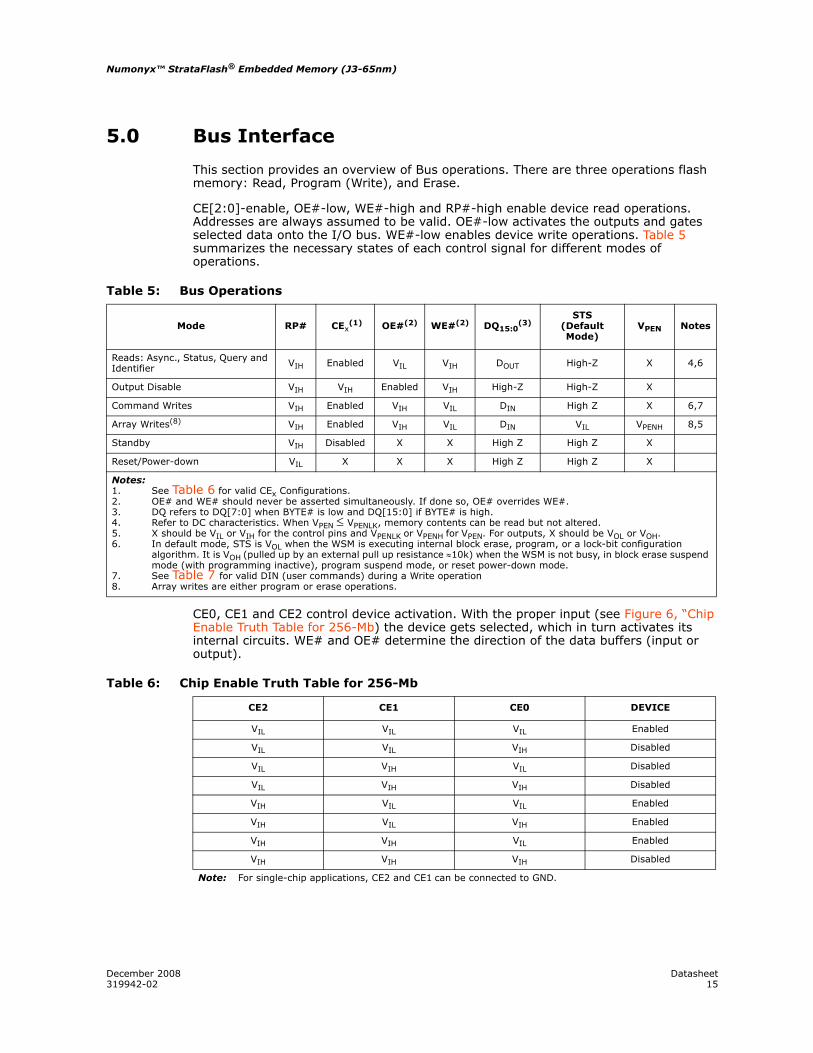
This section provides an overview of Bus operations. There are three operations flash memory: Read, Program (Write), and Erase.
CE[2:0]-enable, OE#-low, WE#-high and RP#-high enable device read operations. Addresses are always assumed to be valid. OE#-low activates the outputs and gates selected data onto the I/O bus. WE#-low enables device write operations. Table 5 summarizes the necessary states of each control signal for different modes of operations.
CE0, CE1 and CE2 control device activation. With the proper input (see Figure 6, “Chip Enable Truth Table for 256-Mb) the device gets selected, which in turn activates its internal circuits. WE# and OE# determine the direction of the data buffers (input or output).
Table 5: Bus Operations
Mode RP# CEx(1) OE#(2) WE#(2) DQ15:0
(3)STS
(Default Mode)
VPEN Notes
Reads: Async., Status, Query and Identifier VIH Enabled VIL VIH DOUT High-Z X 4,6
Output Disable VIH VIH Enabled VIH High-Z High-Z X
Command Writes VIH Enabled VIH VIL DIN High Z X 6,7
Array Writes(8) VIH Enabled VIH VIL DIN VIL VPENH 8,5
Standby VIH Disabled X X High Z High Z X
Reset/Power-down VIL X X X High Z High Z X
Notes:1. See Table 6 for valid CEx Configurations.2. OE# and WE# should never be asserted simultaneously. If done so, OE# overrides WE#.3. DQ refers to DQ[7:0] when BYTE# is low and DQ[15:0] if BYTE# is high.4. Refer to DC characteristics. When VPEN ≤ VPENLK, memory contents can be read but not altered.5. X should be VIL or VIH for the control pins and VPENLK or VPENH for VPEN. For outputs, X should be VOL or VOH.6. In default mode, STS is VOL when the WSM is executing internal block erase, program, or a lock-bit configuration
algorithm. It is VOH (pulled up by an external pull up resistance ≈10k) when the WSM is not busy, in block erase suspend mode (with programming inactive), program suspend mode, or reset power-down mode.
7. See Table 7 for valid DIN (user commands) during a Write operation8. Array writes are either program or erase operations.
Table 6: Chip Enable Truth Table for 256-Mb
CE2 CE1 CE0 DEVICE
VIL VIL VIL Enabled
VIL VIL VIH Disabled
VIL VIH VIL Disabled
VIL VIH VIH Disabled
VIH VIL VIL Enabled
VIH VIL VIH Enabled
VIH VIH VIL Enabled
VIH VIH VIH Disabled
Note: For single-chip applications, CE2 and CE1 can be connected to GND.
Numonyx™ StrataFlash® Embedded Memory (J3-65nm)
Datasheet December 200816 319942-02
5.1 Reads
Reading from flash memory outputs stored information to the processor or chipset, and does not change any contents. Reading can be performed an unlimited number of times. Besides array data, other types of data such as device information or device status are available from the flash.
To perform a bus read operation, CEx (refer to Table 6 on page 15) and OE# must be asserted. CEx is the device-select control; when active, it enables the flash memory device. OE# is the data-output control; when active, the addressed flash memory data is driven onto the I/O bus. For all read states, WE# and RP# must be de-asserted. See Section 7.0, “Read operation” on page 21.
5.2 Writes
Writing or Programming to the device is where the host writes information or data into the flash device for non-volatile storage. When the flash device is programmed, ‘ones’ are changed to ‘zeros’. ‘Zeros’ cannot be programmed back to ‘ones’. To do so, an erase operation must be performed. Writing commands to the Command User Interface (CUI) enables various modes of operation, including the following:
• Reading of array data
• Common Flash Interface (CFI) data
• Identifier codes, inspection, and clearing of the Status Register
Erasing is performed on a block basis – all flash cells within a block are erased together. Any information or data previously stored in the block will be lost. Erasing is typically done prior to programming. The Block Erase command requires appropriate command data and an address within the block to be erased. The Byte/Word Program command requires the command and address of the location to be written. Set Block Lock-Bit commands require the command and block within the device to be locked. The Clear Block Lock-Bits command requires the command and address within the device to be cleared.
The CUI does not occupy an addressable memory location. It is written when the device is enabled and WE# is active. The address and data needed to execute a command are latched on the rising edge of WE# or the first edge of CE0, CE1, or CE2 that disables the device (see Table 6 on page 15). Standard microprocessor write timings are used.
5.3 Output Disable
With CEx asserted, and OE# at a logic-high level (VIH), the device outputs are disabled. Output signals D[15:0] are placed in a high-impedance state.
5.4 Standby
CE0, CE1, and CE2 can disable the device (see Table 6 on page 15) and place it in standby mode. This manipulation of CEx substantially reduces device power consumption. D[15:0] outputs are placed in a high-impedance state independent of OE#. If deselected during block erase, program, or lock-bit configuration, the WSM continues functioning, and consuming active power until the operation completes.
December 2008 Datasheet319942-02 17
Numonyx™ StrataFlash® Embedded Memory (J3-65nm)
5.5 Reset
RP# at VIL initiates the reset/power-down mode.
In read modes, RP#-low deselects the memory, places output drivers in a high-impedance state, and turns off numerous internal circuits. RP# must be held low for a minimum of tPLPH. Time tPHQV is required after return from reset mode until initial memory access outputs are valid. After this wake-up interval, normal operation is restored. The CUI is reset to read array mode and Status Register is set to 0080h.
During Block Erase, Program, or Lock-Bit Configuration modes, RP#-low will abort the operation. In default mode, STS transitions low and remains low for a maximum time of tPLPH + tPHRH until the reset operation is complete. Memory contents being altered are no longer valid; the data may be partially corrupted after a program or partially altered after an erase or lock-bit configuration. Time tPHWL is required after RP# goes to logic-high (VIH) before another command can be written.
As with any automated device, it is important to assert RP# during system reset. When the system comes out of reset, it expects to read from the flash memory. Automated flash memories provide status information when accessed during Block Erase, Program, or Lock-Bit Configuration modes. If a CPU reset occurs with no flash memory reset, proper initialization may not occur because the flash memory may be providing status information instead of array data. Numonyx Flash memories allow proper initialization following a system reset through the use of the RP# input. In this application, RP# is controlled by the same RESET# signal that resets the system CPU.
Numonyx™ StrataFlash® Embedded Memory (J3-65nm)
Datasheet December 200818 319942-02
6.0 Command Set
6.1 Device Command Codes
The system Central Processing Unit provides control of all in-system read, write, and erase operations of the device via the system bus. The on-chip WSM manages all block-erase and program algorithms.
Device commands are written to the CUI to control all flash memory device operations. The CUI does not occupy an addressable memory location; it is the mechanism through which the flash device is controlled. Table 7 shows valid device command codes and descriptions.
Table 7: Command Codes and Definitions (Sheet 1 of 2)
Mode Code Device Mode Description
Read
0xFF Read Array Places the device in Read Array mode. Array data is output on DQ[15:0].
0x70 Read Status Register Places the device in Read Status Register mode. The device enters this mode after a program or erase command is issued. SR data is output on DQ[7:0].
0x90Read Device ID or Configuration Register
Places device in Read Device Identifier mode. Subsequent reads output manufacturer/device codes, Configuration Register data, Block Lock status, or OTP register data on DQ[15:0].
0x98 Read Query Places the device in Read Query mode. Subsequent reads output Common Flash Interface information on DQ[7:0].
0x50 Clear Status Register The WSM can only set SR error bits. The Clear Status Register command is used to clear the SR error bits.
Progra
m
0x40 Word/Byte Program Setup
First cycle of a 2-cycle programming command, prepares the CUI for a write operation. On the next write cycle, the address and data are latched and the WSM executes the programming algorithm at the addressed location. During program operations, the device responds only to Read Status Register and Program Suspend commands. CEX or OE# must be toggled to update the Status Register in asynchronous read. CEX must be toggled to update the SR Data for synchronous Non-array reads. The Read Array command must be issued to read array data after programming has finished.
0xE8 Buffered Program This command loads a variable number of words up to the buffer size of 512 words onto the program buffer in x16 mode. (1)
0xD0 Program ConfirmThe confirm command is Issued after the data streaming for writing into the buffer is done. This instructs the WSM to perform the Buffered Program algorithm, writing the data from the buffer to the flash memory array.
Era
se
0x20 Block Erase Setup
First cycle of a 2-cycle command; prepares the CUI for a block-erase operation. The WSM performs the erase algorithm on the block addressed by the Erase Confirm command. If the next command is not the Erase Confirm (0xD0) command, the CUI sets Status Register bits SR [5,4], and places the device in Read Status Register mode.
0xD0 Block Erase Confirm
If the first command was Block Erase Setup (0x20), the CUI latches the address and data, and the WSM erases the addressed block. During block-erase operations, the device responds only to Read Status Register and Erase Suspend commands. CEX or OE# must be toggled to update the Status Register in asynchronous read. CEX must be toggled to update the SR Data for synchronous Non-array reads.
Susp
end 0xB0 Program or Erase
Suspend
This command issued to any device address initiates a suspend of the currently-executing program or block erase operation. The Status Register indicates successful suspend operation by setting either SR.2 (program suspended) or SR 6 (erase suspended), along with SR.7 (ready). The WSM remains in the suspend mode regardless of control signal states (except for RPRP# asserted).
0xD0 Suspend Resume This command issued to any device address resumes the suspended program or block-erase operation.
December 2008 Datasheet319942-02 19
Numonyx™ StrataFlash® Embedded Memory (J3-65nm)
6.2 Device Command Bus Cycle
Device operations are initiated by writing specific device commands to the CUI. See Table 8, “Command Bus Cycles” on page 19. Several commands are used to modify array data including Word Program and Block Erase commands. Writing either command to the CUI initiates a sequence of internally-timed functions that culminate in the completion of the requested task. However, the operation can be aborted by either asserting RP# or by issuing an appropriate suspend command.
Pro
tect
ion
0x60 Block lock SetupFirst cycle of a 2-cycle command; prepares the CUI for block lock configuration changes. If the next command is not Block Lock (0x01), Block Unlock (0xD0), the CUI sets SR.5 and SR.4, indicating a command sequence error.
0x01 Block lock If the previous command was Block Lock Setup (0x60), the addressed block is locked.
0xD0 Unlock Block If the previous command was Block Lock Setup (0x60), on issuing this command, all of the Block lock bits that are set are cleared in parallel.
0xC0 Protection program setup
First cycle of a 2-cycle command; prepares the device for a OTP register or Lock Register program operation. The second cycle latches the register address and data, and starts the programming algorithm to program data the OTP array.
0xEB Extended Function Interface (EFI)
This command is used in security features. first cycle of a multiple-cycle command second cycle is a Sub-Op-Code, the data written on third cycle is one less than the word count; the allowable value on this cycle are 0 through 511. The subsequent cycles load data words into the program buffer at a specified address until word count is achieved.
For additional information and collateral request, please contact your filed.
STS C
onfigura
tion
B8h Configuration Set-Up
Configures the STS pin to different states. The default operation of the STS pin isthe level mode, just like RY/BY# which indicates if the Write State Machine is Busyor Available. Using this command the STS pin can be configured to generate anErase/Program interrupt pulse once the operation is done.
00h
Configuration Code
Configures the STS pin in level mode. Makes the STS pin function like a RY/BY#pin.
01h Configures the STS pin to generate a pulse once an erase operation is completed.
02h The STS pin is configured to generate a pulse once a program operation completes.
03h The STS pin is configured to generate a pulse when either a program or eraseoperation completes.
Table 7: Command Codes and Definitions (Sheet 2 of 2)
Mode Code Device Mode Description
Table 8: Command Bus Cycles (Sheet 1 of 2)
Mode Command BusCycles
First Bus Cycle Second Bus Cycle Last Bus Cycle
Addr(1) Data(2) Addr(1) Data(2) Addr(1) Data(2)
Read
Read Array 1 DnA 0xFF --- --- --- ---
Read Status Register 2 DnA 0x70 DnA SRD --- ---
Read Device Identifier ≥ 2 DnA 0x90 DBA + IA ID --- ---
Read CFI ≥ 2 DnA 0x98 DBA + CFI-A CFI-D --- ---
Clear Status Register 1 DnA 0x50 --- --- --- ---
Pro
gra
m Word Program 2 WA 0x40 WA WD --- ---
Buffered Program(3) > 2 WA 0xE8 WA N - 1 WA 0xD0
Numonyx™ StrataFlash® Embedded Memory (J3-65nm)
Datasheet December 200820 319942-02
Era
se Block Erase 2 BA 0x20 BA 0xD0 --- ---
Su
spen
d Program/Erase Suspend 1 DnA 0xB0 --- --- --- ---
Program/Erase Resume 1 DnA 0xD0 --- --- --- ---
Pro
tect
ion
Lock Block 2 BA 0x60 BA 0x01 --- ---
Unlock Block 2 BA 0x60 BA 0xD0 --- ---
Program OTP register 2 OTP-RA 0xC0 OTP-RA OTP-D --- ---
Program Lock Register 2 LRA 0xC0 LRA LRD --- ---
STS Configuration 2 BA 0xB8 BA Register Data --- ---
Extended Flash Interface (4) > 2 WA 0xEB WA Sub-Op code WA 0xD0
Notes:1. First command cycle address should be the same as the operation’s target address.
DBA = Device Base Address DnA = Address within the device.IA = Identification code address offset.CFI-A = Read CFI address offset.WA = Word address of memory location to be written.BA = Address within the block.OTP-RA = OTP register address.LRA = Lock Register address.RCD = Read Configuration Register data on A[15:0].
2. ID = Identifier data.CFI-D = CFI data on DQ[15:0].SRD = Status Register data.WD = Word data.N = Word count of data to be loaded into the write buffer.OTP-D = OTP register data.LRD = Lock Register data.
3. The second cycle of the Buffered Program Command is the word count of the data to be loaded into the write buffer. This is followed by up to 512 words of data.Then the confirm command (0xD0) is issued, triggering the array programming operation.
4. The second cycle is a Sub-Op-Code, the data written on third cycle is N-1; 1=<N<=512. The subsequent cycles load data words into the program buffer at a specified address until word count is achieved, after the data words are loaded, the final cycle is the confirm cycle 0xD0)
Table 8: Command Bus Cycles (Sheet 2 of 2)
Mode Command BusCycles
First Bus Cycle Second Bus Cycle Last Bus Cycle
Addr(1) Data(2) Addr(1) Data(2) Addr(1) Data(2)
December 2008 Datasheet319942-02 21
Numonyx™ StrataFlash® Embedded Memory (J3-65nm)
7.0 Read operation
The device can be in any of four read states: Read Array, Read Identifier, Read Status Register or Read Query. Upon power-up, or after a reset, the device defaults to Read Array mode. To change the read state, the appropriate read command must be written to the device (see Section 6.1, “Device Command Codes” on page 18). The following sections describe read-mode operations in detail.
7.1 Read Array
Upon power-up or return from reset, the device defaults to Read Array mode. Issuing the Read Array command places the device in Read Array mode. Subsequent reads output array data on DQ[15:0]. The device remains in Read Array mode until a different read command is issued, or a program or erase operation is performed, in which case, the read mode is automatically changed to Read Status.
To change the device to Read Array mode while it is programming or erasing, first issue the Suspend command. After the operation has been suspended, issue the Read Array command. When the program or erase operation is subsequently resumed, the device will automatically revert back to Read Status mode.
Note: Issuing the Read Array command to the device while it is actively programming or erasing causes subsequent reads from the device to output invalid data. Valid array data is output only after the program or erase operation has finished.
The Read Array command functions independent of the voltage level on VPEN.
7.2 Asynchronous Page Mode Read
J3-65nm supports asynchronous page mode read access only. J3-65nm also supports Byte or Word accesses depending on the level of BYTE#.
• If BYTE# is at VIL then the data will be outputted on the DQ7-0. This read access is called “x8 mode”. The DQ15-8 signals will be in high-z.
• If BYTE# is at VIH then the data will be outputted on DQ15-0.This read access is called “x16 mode.”
The default read mode of the device after power up or hardware reset is read array mode.The Read Array/ Software Reset command returns the device to read array mode. Any following read accesses to devices returns main array data.
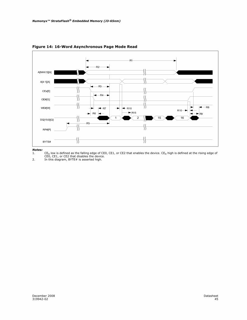
The page size is sixteen words (32 bytes). Each read operation internally retrieves sixteen words of data, which are determined by addressed bits A[MAX:5].In x16 mode, the first word of data, defined by A[4:1], is output to the data bus within tAVQV. After this initial access time, subsequent words can be output to the data bus by changing address bits A[4:1]. In x8 mode, the first byte of data, defined by A[4:0], is output to the data bus within tAVQV. After this initial access time, subsequent bytes can be output to the data bus by changing address bits A[4:0]. Any subsequent data word(s) within the page can be output to the data bus within tAPA, which is much shorter than tAVQV. The internal read operation can also be initiated by asserting CEX while addresses are valid or changing the A[MAX:5] while CEX is asserted.
Numonyx™ StrataFlash® Embedded Memory (J3-65nm)
Datasheet December 200822 319942-02
7.3 Read Status Register
Issuing the Read Status Register command places the device in Read Status Register mode. Subsequent reads output Status Register information on DQ[7:0], and 00h on DQ[15:8]. The device remains in Read Status Register mode until a different read-mode command is issued. Performing a program, erase, or block-lock operation also changes the device’s read mode to Read Status Register mode.
The Status Register is updated on the falling edge of CE, or OE# when CE is active. Status Register contents are valid only when SR.7 = 1. When WSM is busy, SR.7 indicates the WSM’s state and SR[6:0] are in high-Z state.
The Read Status Register command functions independent of the voltage level on VPEN.
7.4 Read Device Information
Issuing the Read Device Information command places the device in Read Device Information mode. Subsequent reads output device information on DQ[15:0].
The device remains in Read Device Information mode until a different read command is issued. Also, performing a program, erase, or block-lock operation changes the device to Read Status Register mode.
The Read Device Information command functions independent of the voltage level on VPEN.
7.5 CFI Query
The CFI query table contains an assortment of flash product information such as block size, density, allowable command sets, electrical specifications, and other product information. The data contained in this table conforms to the CFI protocol.
Table 9: Device Identifier Information
Item Address(1,2,3) Data
Manufacturer Code 0x00 0x89h
Device ID Code 0x01 ID (see Table 1)
Block Lock Configuration:
BBA + 0x02
Lock Bit:
• Block Is Unlocked DQ0 = 0b0
• Block Is Locked DQ0 = 0b1
J3A Block Lock Compatibility 0x03 0x000 (4)
General Purpose Register(5) DBA + 0x07 general data
Lock Register 0 0x80 PR-LK0
64-bit Factory-Programmed OTP register 0x81–0x84 Factory OTP register data
64-bit User-Programmable OTP Register 0x85–0x88 User OTP register data
Notes:1. BBA = Block Base Address.2. DBA = Device base Address, Numonyx reserves other configuration address locations3. A0 is not used in either x8 or x16 modes during manufacturer and device ID reads. The lowest order
address line is A1.4. When reading Block Base Address + 00003h, the user needs to read 0000h to be backward
compatibly to J3A.5. The GPR is used as read out register for Extended Functional Interface (EFI) command.
December 2008 Datasheet319942-02 23
Numonyx™ StrataFlash® Embedded Memory (J3-65nm)
Issuing the CFI Query command places the device in CFI Query mode. Subsequent reads output CFI information on DQ[15:0]. The device remains in CFI Query mode until a different read command is issued, or a program or erase operation is performed, which changes the read mode to Read Status Register mode.
The CFI Query command functions independent of the voltage level on VPEN.
Numonyx™ StrataFlash® Embedded Memory (J3-65nm)
Datasheet December 200824 319942-02
8.0 Program operation
All programming operations require the addressed block to be unlocked, and a valid VPEN voltage applied throughout the programming operation. Otherwise, the programming operation will abort, setting the appropriate Status Register error bit(s).
The following sections describe each programming method.
8.1 Single-Word/Byte Programming
Array programming is performed by first issuing the Single-Word/Byte Program command. This is followed by writing the desired data at the desired array address. The read mode of the device is automatically changed to Read Status Register mode, which remains in effect until another read-mode command is issued.
During programming, STS and the Status Register indicate a busy status (SR.7 = 0). Upon completion, STS and the Status Register indicate a ready status (SR.7 = 1). The Status Register should be checked for any errors (SR.4), then cleared.
Note: Issuing the Read Array command to the device while it is actively programming causes subsequent reads from the device to output invalid data. Valid array data is output only after the program operation has finished.
Standby power levels are not realized until the programming operation has finished. Also, asserting RP# aborts the programming operation, and array contents at the addressed location are indeterminate. The addressed block should be erased, and the data re-programmed. If a Single-Word/Byte program is attempted when the corresponding block lock-bit is set, SR.1 and SR.4 will be set.
8.2 Buffered Programming
The device features a 512-word buffer to enable optimum programming performance. For Buffered Programming, data is first written to an on-chip write buffer. Then the buffer data is programmed into the flash memory array in buffer-size increments. This can improve system programming performance significantly over non-buffered programming. (see Figure 19, “Buffer Program Flowchart” on page 59).
When the Buffered Programming Setup command is issued, Status Register information is updated and reflects the availability of the buffer. SR.7 indicates buffer availability: if set, the buffer is available; if cleared, the buffer is not available. To retry, issue the Buffered Programming Setup command again, and re-check SR.7. When SR.7 is set, the buffer is ready for loading.
On the next write, a word count is written to the device at the buffer address. This tells the device how many data words will be written to the buffer, up to the maximum size of the buffer.
On the next write, a device start address is given along with the first data to be written to the flash memory array. Subsequent writes provide additional device addresses and data. All data addresses must lie within the start address plus the word count.
Optimum programming performance and lower power usage are obtained by aligning the starting address at the beginning of a 512-word boundary (A[9:1] = 0x00). The maximum buffer size would be 256-word if the misaligned address range is crossing a 512-word boundary during programming.
After the last data is written to the buffer, the Buffered Programming Confirm command must be issued to the original block address. The WSM begins to program buffer contents to the flash memory array. If a command other than the Buffered
December 2008 Datasheet319942-02 25
Numonyx™ StrataFlash® Embedded Memory (J3-65nm)
Programming Confirm command is written to the device, a command sequence error occurs and SR[7,5,4] are set. If an error occurs while writing to the array, the device stops programming, and SR[7,4] are set, indicating a programming failure.
When Buffered Programming has completed, additional buffer writes can be initiated by issuing another Buffered Programming Setup command and repeating the buffered program sequence.
If an attempt is made to program past an erase-block boundary using the Buffered Program command, the device aborts the operation. This generates a command sequence error, and SR[5,4] are set.
If Buffered programming is attempted while VPEN is below VPENLK, SR[4,3] are set. If any errors are detected that have set Status Register bits, the Status Register should be cleared using the Clear Status Register command.
Note: In x8 mode, a maximum of 256 bytes of data can be loaded into the write buffer as N can have a max value of FFh.
8.3 Suspend/Resume
An erase or programming operation can be suspended to perform other operations, and then subsequently resumed. Please refer to Chapter 9.0, “Suspend/Resume” for details.
Numonyx™ StrataFlash® Embedded Memory (J3-65nm)
Datasheet December 200826 319942-02
9.0 Erase Operation
Flash erasing is performed on a block basis. An entire block is erased each time an erase command sequence is issued, and only one block is erased at a time. When a block is erased, all bits within that block read as logical ones. The following sections describe block erase operations in detail.
9.1 Block Erase
Erasing a block changes ‘zeros’ to ‘ones’. To change ones to zeros, a program operation must be performed (see Section 8.0, “Program operation”). Erasing is performed on a block basis - an entire block is erased each time an erase command sequence is issued. Once a block is fully erased, all addressable locations within that block read as logical ones (FFFFh). Only one block-erase operation can occur at a time, and is not permitted during a program suspend (see Figure 21, “Block Erase Flowchart” on page 61).
Note: A block-erase operation requires the addressed block to be unlocked, and a valid voltage applied to VPEN throughout the block-erase operation. Otherwise, the operation will abort, setting the appropriate Status Register error bit(s).
The Erase Confirm command latches the address of the block to be erased. The addressed block is preconditioned (programmed to all zeros), erased, and then verified. The read mode of the device is automatically changed to Read Status Register mode, and remains in effect until another read-mode command is issued.
During a block-erase operation, STS and the Status Register indicates a busy status (SR.7 = 0). Upon completion, STS and the Status Register indicates a ready status (SR.7 = 1). The Status Register should be checked for any errors, then cleared. If any errors did occur, subsequent erase commands to the device are ignored unless the Status Register is cleared.
The only valid commands during a block erase operation are Read Status and Erase Suspend. After the block-erase operation has completed, any valid command can be issued.
Note: Issuing the Read Array command to the device while it is actively erasing causes subsequent reads from the device to output invalid data. Valid array data is output only after the block-erase operation has finished.
Standby power levels are not realized until the block-erase operation has finished. Also, asserting RP# aborts the block-erase operation, and array contents at the addressed location are indeterminate. The addressed block should be erased before programming within the block is attempted.
9.2 Suspend/Resume
An erase or programming operation can be suspended to perform other operations, and then subsequently resumed. Table 8 shows the Suspend and Resume command bus-cycles (see Figure 18, “Program/Erase Suspend/Resume Flowchart” on page 57).
Note: All erase and programming operations require the addressed block to remain unlocked with a valid voltage applied to VPEN throughout the suspend operation. Otherwise, the block-erase or programming operation will abort, setting the appropriate Status Register error bit(s). Also, asserting RP# aborts suspended block-erase and programming operations, rendering array contents at the addressed location(s) indeterminate.
December 2008 Datasheet319942-02 27
Numonyx™ StrataFlash® Embedded Memory (J3-65nm)
To suspend an on-going erase or program operation, issue the Suspend command to any device address. The program or erase operation suspends at pre-determined points during the operation after a delay of tSUSP. Suspend is achieved when STS (in RY/BY# mode) goes high, SR[7,6] = 1 (erase-suspend) or SR[7,2] = 1 (program-suspend).
Note: Issuing the Suspend command does not change the read mode of the device. The device will be in Read Status Register mode from when the erase or program command was first issued, unless the read mode was changed prior to issuing the Suspend command.
Not all commands are allowed when the device is suspended. Table 10 shows which device commands are allowed during Program Suspend or Erase Suspend.
During Suspend, array-read operations are not allowed in blocks being erased or programmed.
A block-erase under program-suspend is not allowed. However, word-program under erase-suspend is allowed, and can be suspended. This results in a simultaneous erase-suspend/ program-suspend condition, indicated by SR[7,6,2] = 1.
To resume a suspended program or erase operation, issue the Resume command to any device address. The read mode of the device is automatically changed to Read Status Register. The operation continues where it left off, STS (in RY/BY# mode) goes low, and the respective Status Register bits are cleared.
When the Resume command is issued during a simultaneous erase-suspend/ program-suspend condition, the programming operation is resumed first. Upon completion of the programming operation, the Status Register should be checked for any errors, and cleared. The resume command must be issued again to complete the erase operation. Upon completion of the erase operation, the Status Register should be checked for any errors, and cleared.
Table 10: Valid Commands During Suspend
Device Command Program Suspend Erase Suspend
STS Configuration Allowed Allowed
Read Array Allowed Allowed
Read Status Register Allowed Allowed
Clear Status Register Allowed Allowed
Read Device Information Allowed Allowed
CFI Query Allowed Allowed
Word/Byte Program Not Allowed Allowed
Buffered Program Not Allowed Allowed
Block Erase Not Allowed Not Allowed
Program Suspend Not Allowed Allowed
Erase Suspend Not Allowed Not Allowed
Program/Erase Resume Allowed Allowed
Lock Block Not Allowed Not Allowed
Unlock Block Not Allowed Not Allowed
Program OTP Register Not Allowed Not Allowed
Numonyx™ StrataFlash® Embedded Memory (J3-65nm)
Datasheet December 200828 319942-02
10.0 Security
J3-65nm device offer both hardware and software security features. Block lock operations, PRs and VPEN allow users to implement various levels of data protection.
10.1 Normal Block Locking
J3-65nm has the unique capability of Flexible Block Locking (locked blocks remain locked upon reset or power cycle): All blocks are unlocked at Numonyx factory. Blocks can be locked individually by issuing the Set Block Lock Bit command sequence to any address within a block. Once locked, blocks remain locked when power is removed, or when the device is reset (see Figure 20, “Block Lock Operations Flowchart” on page 60).
All locked blocks are unlocked simultaneously by issuing the Clear Block Lock Bits command sequence to any device address. Locked blocks cannot be erased or programmed. Table 8 summarizes the command bus-cycles.
After issuing the Set Block Lock Bit setup command or Clear Block Lock Bits setup command, the device’s read mode is automatically changed to Read Status Register mode. After issuing the confirm command, completion of the operation is indicated by STS (in RY/BY# mode) going high and SR.7 = 1.
Blocks cannot be locked or unlocked while programming or erasing, or while the device is suspended. Reliable block lock and unlock operations occur only when VCC and VPEN are valid. When VPEN ≤ VPENLK, block lock-bits cannot be changed.
When the set lock-bit operation is complete, SR.4 should be checked for any error. When the clear lock-bit operation is complete, SR.5 should be checked for any error. Errors bits must be cleared using the Clear Status Register command.
Block lock-bit status can be determined by first issuing the Read Device Information command, and then reading from <block base address> + 02h. DQ0 indicates the lock status of the addressed block (0 = unlocked, 1 = locked).
10.2 Configurable Block Locking
One of the unique new features on the J3-65nm,which did not exist on the previous generations of this product family, is the ability to protect and/or secure the user’s system by offering multiple level of securities: Non-Volatile Temporary; Non-Volatile Semi-Permanent or Non-Volatile Permanent. For additional information and collateral request, please contact your filed representative .
December 2008 Datasheet319942-02 29
Numonyx™ StrataFlash® Embedded Memory (J3-65nm)
10.3 VPEN Protection
When it’s necessary to protect the entire array, global protection can be achieved using a hardware mechanism using VPEN. Whenever a valid voltage is present on VPEN, blocks within the main flash array can be erased or programmed. By grounding VPEN, blocks within the main array cannot be altered – attempts to program or erase blocks will fail resulting in the setting of the appropriate error bit in the Status Register. By holding VPEN low, absolute write protection of all blocks in the array can be achieved.
10.4 Password Access
Password Access is a security enhancement offered on the J3-65nm device. This feature protects information stored in main-array memory blocks by preventing content alteration or reads, until a valid 64-bit password is received. Password Access may be combined with Non-Volatile Protection and/or Volatile Protection to create a multi-tiered solution.
Please contact your Numonyx Sales for further details concerning Password Access.
Numonyx™ StrataFlash® Embedded Memory (J3-65nm)
Datasheet December 200830 319942-02
11.0 Registers
11.1 Status Register
The Status Register (SR) is an 8-bit, read-only register that indicates device status and operation errors. To read the Status Register, issue the Read Status Register command. Subsequent reads output Status Register information on DQ[7:0], and 00h on DQ[15:8].
SR status bits are set and cleared by the device. SR error bits are set by the device, but must be cleared using the Clear Status Register command. Upon power-up or exit from reset, the Status Register defaults to 80h. Page-mode reads are not supported in this read mode. Status Register contents are latched on the falling edge of OE# or the first edge of CEx that enables the device. OE# must toggle to VIH or the device must be disabled before further reads to update the Status Register latch. The Read Status Register command functions independently of VPEN voltage.Table 11 shows Status Register bit definitions.
Table 11: Status Register Description
Status Register (SR) Default Value = 0x80
Device Write Status
Erase Suspend Status Erase Status Program
StatusProg/Erase
Voltage Error
Program Suspend Status
Block-Locked Status Reserved
DWS ESS ES PS PEVE PSS BLS
7 6 5 4 3 2 1 0
Bit Name Description
7 Device Write Status (DWS)0 = Device is busy; program or erase cycle in progress.1 = Device is ready; SR[6:1] are valid.
6 Erase Suspend Status (ESS)0 = Erase suspend not in effect.1 = Erase suspend in effect.
5 Erase Status (ES)0 = Erase successful.1 = Erase fail or program sequence error when set with SR.4,SR.7.
4 Program Status (PS)0 = Program successful.1 = Program fail or program sequence error when set with SR.5,SR.7
3 Prog/Erase Voltage Error (PEVE)0 = VPEN within acceptable limits during program or erase operation.1 = VPEN ≤ VPENLK during program or erase operation.
2 Program Suspend Status (PSS)0 = Program suspend not in effect.1 = Program suspend in effect.
1 Block-Locked Status (BLS)0 = Block not locked during program or erase.1 = Block locked during program or erase; operation aborted.
0 Reserved 0 = Default
Note: Always clear the Status Register prior to resuming erase operations. It avoids Status Register ambiguity when issuing commands during Erase Suspend. If a command sequence error occurs during an erase-suspend state, the Status Register contains the command sequence error status (SR[7,5,4] set). When the erase operation resumes and finishes, possible errors during the erase operation cannot be detected via the Status Register because it contains the previous error status
December 2008 Datasheet319942-02 31
Numonyx™ StrataFlash® Embedded Memory (J3-65nm)
11.1.1 Clearing the Status Register
The Clear Status Register command clears the status register. It functions independent of VPEN. The WSM sets and clears SR[7,6,2], but it sets bits SR[5:3,1] without clearing them. The Status Register should be cleared before starting a command sequence to avoid any ambiguity. A device reset also clears the Status Register.
11.2 Status Signal
The STATUS (STS) signal can be configured to different states using the STS Configuration command (Table 12). Once the STS signal has been configured, it remains in that configuration until another Configuration command is issued or RP# is asserted low. Initially, the STS signal defaults to RY/BY# operation where RY/BY# low indicates that the WSM is busy. RY/BY# high indicates that the state machine is ready for a new operation or suspended. Table 12 displays possible STS configurations.
To reconfigure the STATUS (STS) signal to other modes, the Configuration command is given followed by the desired configuration code. The three alternate configurations are all pulse mode for use as a system interrupt as described in the following paragraphs. For these configurations, bit 0 controls Erase Complete interrupt pulse, and bit 1 controls Program Complete interrupt pulse. Supplying the 00h configuration code with the Configuration command resets the STS signal to the default RY/BY# level mode. The Configuration command may only be given when the device is not busy or suspended. Check SR.7 for device status. An invalid configuration code will result in SR.4 and SR.5 being set.
Note: STS Pulse mode is not supported in the Clear Lock Bits and Set Lock Bit commands.
Numonyx™ StrataFlash® Embedded Memory (J3-65nm)
Datasheet December 200832 319942-02
11.3 OTP Protection Register
J3-65nm includes a 128-bit Protection Register (PR) that can be used to increase the security of a system design. For example, the number contained in the PR can be used to “match” the flash component with other system components such as the CPU or ASIC, hence preventing device substitution.
The 128-bits of the PR are divided into two 64-bit segments:
• One segment is programmed at the Numonyx factory with a unique unalterable 64-bit number.
• The other segment is left blank for customer designers to program as desired. Once the customer segment is programmed, it can be locked to prevent further programming.
11.3.1 Reading the OTP Protection Register
The Protection Register is read in Identification Read mode. The device is switched to this mode by issuing the Read Identifier command (0090h). Once in this mode, read cycles from addresses shown in Table 13, “Word-Wide Protection Register Addressing” or Table 14, “Byte-Wide Protection Register Addressing” retrieve the specified information. To return to Read Array mode, write the Read Array command (00FFh).
11.3.2 Programming the OTP Protection Register
PR bits are programmed using the two-cycle Protection Program command. The 64-bit number is programmed 16 bits at a time for word-wide configuration and eight bits at a time for byte-wide configuration. First write the Protection Program Setup command, 00C0h. The next write to the device will latch in address and data and program the specified location. The allowable addresses are shown in Table 13, “Word-Wide
Table 12: STS Configuration Coding Definitions
D7 D6 D5 D4 D3 D2 D1 D0
Reserved3
Pulse on Program Complete
(1)
Pulse on Erase
Complete (1)
D[1:0] = STS Configuration Codes Notes
00 = default, level mode;device ready indication
Controls HOLD to a memory controller to prevent accessing a flash memory subsystem while any flash device's WSM is busy.
01 = pulse on Erase CompleteGenerates a system interrupt pulse when any flash device in an array has completed a block erase. Helpful for reformatting blocks after file system free space reclamation or “cleanup.”
10 = pulse on Program CompleteGenerate a system interrupt pulse when any flash device in an array has complete a Program operation. Provides highest performance for servicing continuous buffer write operations.
11 = pulse on Erase or Program CompleteGenerates system interrupts to trigger servicing of flash arrays when either erase or program operations are completed, when a common interrupt service routine is desired.
Notes:1. When configured in one of the pulse modes, STS pulses low with a typical pulse width of 500 ns.2. An invalid configuration code will result in both SR.4 and SR.5 being set.3. Reserved bits are invalid should be ignored.
December 2008 Datasheet319942-02 33
Numonyx™ StrataFlash® Embedded Memory (J3-65nm)
Protection Register Addressing” on page 33 or Table 14, “Byte-Wide Protection Register Addressing” on page 34. See Figure 22, “OTP Register Programming Flowchart” on page 62. Any attempt to address Protection Program commands outside the defined PR address space will result in a Status Register error (SR.4 will be set). Attempting to program a locked PR segment will result in a Status Register error (SR.4 and SR.1 will be set).
11.3.3 Locking the OTP Protection Register
The user-programmable segment of the PR is lockable by programming Bit 1 of the Protection Lock Register (PLR) to 0. Bit 0 of this location is programmed to 0 at the Numonyx factory to protect the unique device number. Bit 1 is set using the Protection Program command to program “0xFFFD” to the PLR. After these bits have been programmed, no further changes can be made to the values stored in the Protection Register. Protection Program commands to a locked section will result in a Status Register error (SR.4 and SR.1 will be set). The PR lockout state is not reversible.
Note: A0 is not used in x16 mode when accessing the protection register map. See Table 13 for x16 addressing. In x8 mode A0 is used, see Table 14 for x8 addressing.
Note: All address lines not specified in the above table must be 0 when accessing the Protection Register, i.e., A[MAX:9] = 0.
December 2008 Datasheet319942-02 35
Numonyx™ StrataFlash® Embedded Memory (J3-65nm)
12.0 Power and Reset Specifications
12.1 Power-Up and Power-Down
Power supply sequencing is not required if VPEN is connected to VCC or VCCQ. Otherwise VCC and VCCQ should attain their minimum operating voltage before applying VPEN.
Power supply transitions should only occur when RP# is low. This protects the device from accidental programming or erasure during power transitions.
12.1.1 Power-Up/Down Characteristics
To prevent conditions that could result in spurious program or erase operations, several valid power-up/power-down sequences shown in Table 15 are recommended. For DC voltage characteristics refer to Table 20. Note that each power supply must reach its minimum voltage range before applying/removing the next supply voltage.
Note: Power supplies connected or sequenced together.
Device inputs must not be driven until all supply voltages reach their minimum range. RP# should be low during power transitions.
Table 15: Power-Up/Down Sequence
Power Supply Voltage Power-Up Sequence Power-Down Sequence
VCC(min) 1st 1st1st† Sequencing not
required†
3rd 2nd2nd†
Sequencing not required†VCCQ(min) 2nd
2nd†2nd
1st†VPEN(min) 3rd 2nd 1st 1st
Numonyx™ StrataFlash® Embedded Memory (J3-65nm)
Datasheet December 200836 319942-02
12.2 Reset Specifications
Asserting RP# during a system reset is important with automated program/erase devices because systems typically expect to read from flash memory when coming out of reset. If a CPU reset occurs without a flash memory reset, proper CPU initialization may not occur. This is because the flash memory may be providing status information, instead of array data as expected. Connect RP# to the same active low reset signal used for CPU initialization.
Also, because the device is disabled when RP# is asserted, it ignores its control inputs during power-up/down. Invalid bus conditions are masked, providing a level of memory protection.
Table 16: Power and Reset
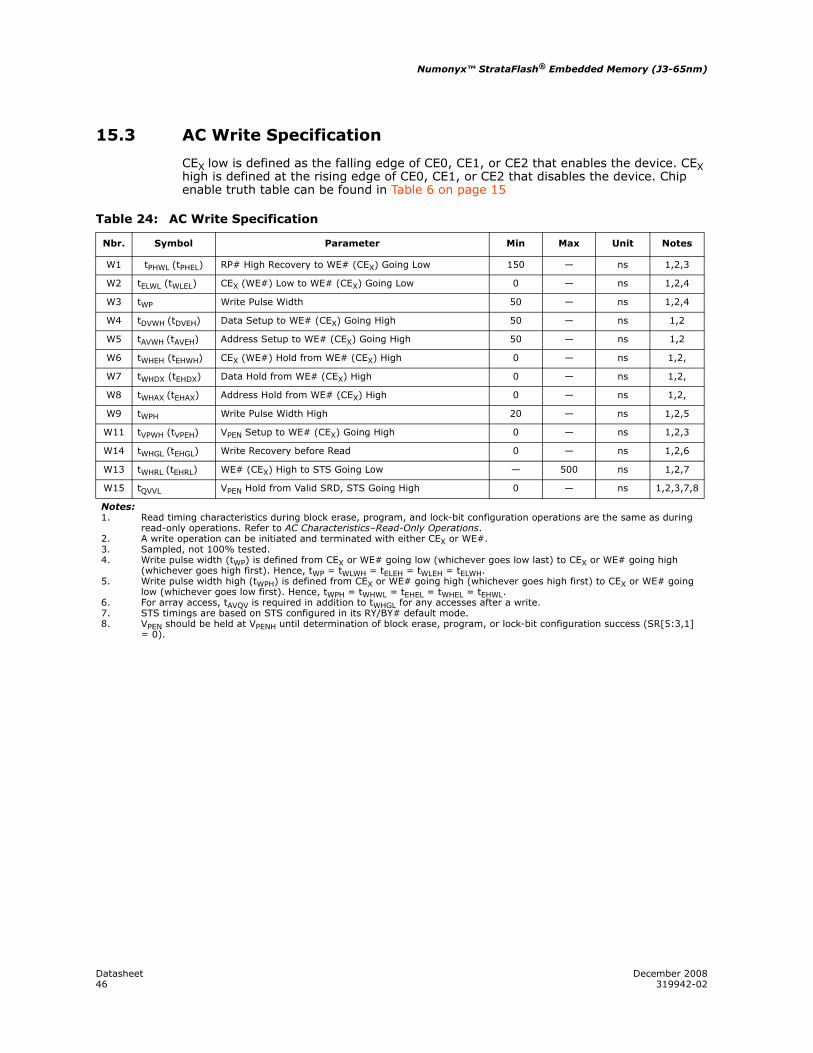
Num Symbol Parameter Min Max Unit Notes
P1 tPLPH RP# pulse width low 100 - ns 1,2,3,4
P2 tPLRH
RP# low to device reset during erase - 25
µs
1,3,4,7
RP# low to device reset during program - 25 1,3,4,7
P3 tVCCPH VCC Power valid to RP# de-assertion (high) 300 - 1,4,5,6
Notes:1. These specifications are valid for all device versions (packages and speeds).2. The device may reset if tPLPH is < tPLPH Min, but this is not guaranteed.3. Not applicable if RP# is tied to VCC.4. Sampled, but not 100% tested.5. When RP# is tied to the VCC supply, device will not be ready until tVCCPH after VCC ≥ VCCMIN. 6. When RP# is tied to the VCCQ supply, device will not be ready until tVCCPH after VCC ≥ VCCMIN.7. Reset completes within tPLPH if RP# is asserted while no erase or program operation is executing.
Figure 7: Reset Operation Waveforms
(A) Reset duringread mode
(B) Reset duringprogram or block eraseP1 ≤ P2
(C) Reset duringprogram or block eraseP1 ≥ P2
VIH
VIL
VIH
VIL
VIH
VIL
RST# [P]
RST# [P]
RST# [P]
AbortComplete
AbortComplete
VCC
0VVCC
(D) VCC Power-up toRST# high
P1 R5
P2
P3
P2 R5
R5
December 2008 Datasheet319942-02 37
Numonyx™ StrataFlash® Embedded Memory (J3-65nm)
12.3 Power Supply Decoupling
Flash memory devices require careful power supply de-coupling. Three basic power supply current considerations are: 1) standby current levels; 2) active current levels; and 3) transient peaks produced when CEX and OE# are asserted and deasserted.
When the device is accessed, many internal conditions change. Circuits within the device enable charge-pumps, and internal logic states change at high speed. All of these internal activities produce transient signals. Transient current magnitudes depend on the device outputs’ capacitive and inductive loading. Two-line control and correct de-coupling capacitor selection suppress transient voltage peaks.
Because Numonyx MLC flash memory devices draw their power from VCC, VSS, and VCCQ, each power connection should have a 0.1 µF ceramic capacitor to ground. High-frequency, inherently low-inductance capacitors should be placed as close as possible to package leads.
Additionally, for every eight devices used in the system, a 4.7 µF electrolytic capacitor should be placed between power and ground close to the devices. The bulk capacitor is meant to overcome voltage droop caused by PCB trace inductance.
Numonyx™ StrataFlash® Embedded Memory (J3-65nm)
Datasheet December 200838 319942-02
13.0 Maximum Ratings and Operating Conditions
13.1 Absolute Maximum Ratings
Warning: Stressing the device beyond the “Absolute Maximum Ratings” may cause permanent damage. These are stress ratings only.
13.2 Operating Conditions
Warning: Operation beyond the “Operating Conditions” is not recommended and extended exposure beyond the “Operating Conditions” may affect device reliability
NOTICE: This document contains information available at the time of its release. The specifications are subject to change without notice. Verify with your local Numonyx sales office that you have the latest datasheet before finalizing a design.
Table 17: Absolute Maximum Ratings
Parameter Min Max Unit Notes
Temperature under Bias Expanded (TA, Ambient) –40 +85 °C —
Storage Temperature –65 +125 °C —
VCC & VCCQ Voltage –2.0 +5.6 V 2
Voltage on any input/output signal (except VCC, VCCQ) –2.0 VCCQ (max) + 2.0 V 1
ISH Output Short Circuit Current — 100 mA 3
Notes:1. Voltage is referenced to VSS. During infrequent non-periodic transitions, the voltage potential between VSS and input/
output pins may undershoot to –2.0 V for periods < 20 ns or overshoot to VCCQ (max) + 2.0 V for periods < 20 ns.2. During infrequent non-periodic transitions, the voltage potential between VCC and the supplies may undershoot to –2.0
V for periods < 20 ns or VSUPPLY (max) + 2.0 V for periods < 20 ns.3. Output shorted must be no more than one second. No more than one output can be shorted at a time.
Table 18: Temperature and VCC Operating Condition
Symbol Parameter Min Max Unit Test Condition
TA Operating Temperature (Amibent) -40 +85 °C Ambient Temperature
VCC VCC Supply Voltage 2.7 3.6 V —
VCCQ I/O Supply Voltage 2.7 3.6 V —
Block Erase Cycles Main Blocks 100k — Cycles —
December 2008 Datasheet319942-02 39
Numonyx™ StrataFlash® Embedded Memory (J3-65nm)
14.0 Electrical characteristics
14.1 DC Current Specifications
Please refer to Figure 6, “Chip Enable Truth Table for 256-Mb” on page 15 to understand the device is disable or enabled.
35 50 mA VPEN = VPENH, program/erase in progress 1,3
ICCWS ICCES
VCC Program SuspendVCC Erase Suspend
Refer to ICCS
µA CE# = VCCQ, suspend in progress 1,4
Notes:1. All currents are in RMS unless otherwise noted. These currents are valid for all product versions (packages and
speeds). 2. Includes STS.3. Sampled, not 100% tested.4. ICCWS and ICCES are specified with the device selected. If the device is read or written while in erase suspend
mode, the device’s current draw is ICCR and ICCWS.
Numonyx™ StrataFlash® Embedded Memory (J3-65nm)
Datasheet December 200840 319942-02
14.2 DC Voltage Specifications
14.3 Capacitance
Table 20: DC Voltage Characteristics
Symbol Parameter2.7 - 3.6 V
Test Conditions NotesMin Max Unit
VIL Input Low Voltage –0.5 0.6 V 2, 5, 6
VIH Input High Voltage 2.0 VCCQ + 0.5V V 2, 5, 6
VOL Output Low Voltage
— 0.4 VVCC = VCCMinVCCQ = VCCQ MinIOL = 2 mA
1, 2
— 0.2 VVCC = VCCMinVCCQ = VCCQ MinIOL = 100 µA
VOH Output High Voltage
0.85 × VCCQ
— VVCC = VCCMINVCCQ = VCCQ MinIOH = –2.5 mA
1, 2
VCCQ – 0.2 — V
VCC = VCCMINVCCQ = VCCQ MinIOH = –100 µA
VPENLKVPEN Lockout during Program, Erase and Lock-Bit Operations — 2.2 V 2, 3
VPENHVPEN during Block Erase, Program, or Lock-Bit Operations 2.7 3.6 V 3
VLKO VCC Lockout Voltage 1.5 — V 4
VLKOQ VCCQ Lockout Voltage 0.9 — V
Notes:1. Includes STS.2. Sampled, not 100% tested.3. Block erases, programming, and lock-bit configurations are inhibited when VPEN ≤ VPENLK, and not guaranteed in the
range between VPENLK (max) and VPENH (min), and above VPENH (max).4. Block erases, programming, and lock-bit configurations are inhibited when VCC < VLKO, and not guaranteed in the
range between VLKO (min) and VCC (min), and above VCC (max).5. Includes all operational modes of the device including standby and power-up sequences6. Input/Output signals can undershoot to -1.0V referenced to VSS and can overshoot to VCCQ + 1.0V for duration of 2ns
or less, the VCCQ valid range is referenced to VSS.
Table 21: Capacitance
Symbol Parameter Signals Min Typ Max Unit Condition Note
CIN Input CapacitanceAddress, Data,
CE#, WE#, OE#, BYTE#,RP#
2 6 7 pFTyp temp = 25 °C, Max temp = 85 °C, VCC = (0 V - 3.6 V),
VCCQ = (0 V - 3.6 V), Discrete silicon die
1,2,3
COUT Output Capacitance Data, STS 2 4 5 pF
Notes:1. Capacitance values are for a single die.2. Sampled, not 100% tested.3. Silicon die capacitance only, add 1 pF for discrete packages.
December 2008 Datasheet319942-02 41
Numonyx™ StrataFlash® Embedded Memory (J3-65nm)
15.0 AC characteristics
Timing symbols used in the timing diagrams within this document conform to the following convention
Note: Exceptions to this convention include tACC and tAPA. tACC is a generic timing symbol that refers to the aggregate initial-access delay as determined by tAVQV, tELQV, and tGLQV (whichever is satisfied last) of the flash device. tAPA is specified in the flash device’s data sheet, and is the address-to-data delay for subsequent page-mode reads.
15.1 AC Test Conditions
Note: AC test inputs are driven at VCCQ for Logic "1" and 0 V for Logic "0." Input/output timing begins/ends at VCCQ/2. Input rise and fall times (10% to 90%) < 5 ns. Worst-case speed occurs at VCC = VCCMin.
Figure 8: Timing Signal Naming Convention
Figure 9: Timing Signal Name Decoder
Signal Code State Code
Address A High H
Data - Read Q Low L
Data - Write D High-Z Z
Chip Enable (CE) E Low-Z X
Output Enable (OE#) G Valid V
Write Enable (WE#) W Invalid I
BYTE# F
Reset (RP#) P
STS R
VPEN V
Et L Q VSource Signal Target StateSource State Target Signal
Figure 10: AC Input/Output Reference Waveform
IO_REF.WMF
Input VCCQ/2 VCCQ/2 Output
VCCQ
0V
Test Points
Numonyx™ StrataFlash® Embedded Memory (J3-65nm)
Datasheet December 200842 319942-02
Notes:1. See the following table for component values.2. Test configuration component value for worst case speed conditions.3. CL includes jig capacitance.
Table 22: Test Configuration Component Value for Worst Case Speed Conditions
Test Configuration CL (pF)
VCCQ Min Standard Test 30
DeviceUnder Test Out
CL
December 2008 Datasheet319942-02 43
Numonyx™ StrataFlash® Embedded Memory (J3-65nm)
15.2 AC Read Specifications
Chip enable truth table can be found on Table 6 on page 15
Test configuration can be found in Table 22 on page 42
Notes:1. CEX low is defined as the falling edge of CE0, CE1, or CE2 that enables the device. CEX high is defined as the rising edge
of CE0, CE1, or CE2 that disables the device 2. See AC Input/Output Reference Waveforms for the maximum allowable input slew rate.3. OE# may be delayed up to tELQV-tGLQV after the falling edge of CE0, CE1, or CE2 that enables the device without impact on
tELQV.4. Sampled, not 100% tested.5. For devices configured to standard word/byte read mode, R15 (tAPA) will equal R2 (tAVQV).
R8 tEHQZ CEX High to Output in High Z — 20 ns 1,2,3,4
R9 tGHQZ OE# High to Output in High Z — 15 ns 1,2,3,4
R10 tOHOutput Hold from Address, CEX, or OE# Change, Whichever Occurs First 0 — ns 1,2,3,4
R11 tELFL/tELFH CEX Low to BYTE# High or Low — 10 ns 1,2,3,4
R12 tFLQV/tFHQV BYTE# to Output Delay — 1 µs 1,2,3
R13 tFLQZ BYTE# to Output in High Z — 1 µs 1,2,3,4
R14 tEHEL CEx High to CEx Low 0 — ns 1,2,3,4
R15 tAPA Page Address Access Time — 25 ns 4, 5
R16 tGLQV OE# to Array Output Delay — 25 ns 1,2,3
Numonyx™ StrataFlash® Embedded Memory (J3-65nm)
Datasheet December 200844 319942-02
Notes:1. CEX low is defined as the falling edge of CE0, CE1, or CE2 that enables the device. CEX high is defined as the rising edge of
CE0, CE1, or CE2 that disables the device.2. When reading the flash array a faster tGLQV (R16) applies. For non-array reads, R4 applies (i.e., Status Register reads,
query reads, or device identifier reads).
Note:1. CEX low is defined as the falling edge of CE0, CE1, or CE2 that enables the device. CEX high is defined as the rising edge of
CE0, CE1, or CE2 that disables the device.2. In this diagram, BYTE# is asserted high.
Notes:1. CEX low is defined as the falling edge of CE0, CE1, or CE2 that enables the device. CEX high is defined at the rising edge of
CE0, CE1, or CE2 that disables the device. 2. In this diagram, BYTE# is asserted high.
Figure 14: 16-Word Asynchronous Page Mode Read
A[MAX:5][A]
1 2 1615
R2
R1
R3
R4
R7
R6
R5
R10
R15R10
R9
R8
A[4:1][A]
CEx[E]
OE#[G]
WE#[W]
DQ[15:0][Q]
RP#[P]
BYTE#
Numonyx™ StrataFlash® Embedded Memory (J3-65nm)
Datasheet December 200846 319942-02
15.3 AC Write Specification
CEX low is defined as the falling edge of CE0, CE1, or CE2 that enables the device. CEX high is defined at the rising edge of CE0, CE1, or CE2 that disables the device. Chip enable truth table can be found in Table 6 on page 15
Table 24: AC Write Specification
Nbr. Symbol Parameter Min Max Unit Notes
W1 tPHWL (tPHEL) RP# High Recovery to WE# (CEX) Going Low 150 — ns 1,2,3
W13 tWHRL (tEHRL) WE# (CEX) High to STS Going Low — 500 ns 1,2,7
W15 tQVVL VPEN Hold from Valid SRD, STS Going High 0 — ns 1,2,3,7,8
Notes:1. Read timing characteristics during block erase, program, and lock-bit configuration operations are the same as during
read-only operations. Refer to AC Characteristics–Read-Only Operations.2. A write operation can be initiated and terminated with either CEX or WE#.3. Sampled, not 100% tested.4. Write pulse width (tWP) is defined from CEX or WE# going low (whichever goes low last) to CEX or WE# going high
(whichever goes high first). Hence, tWP = tWLWH = tELEH = tWLEH = tELWH.5. Write pulse width high (tWPH) is defined from CEX or WE# going high (whichever goes high first) to CEX or WE# going
low (whichever goes low first). Hence, tWPH = tWHWL = tEHEL = tWHEL = tEHWL.6. For array access, tAVQV is required in addition to tWHGL for any accesses after a write.7. STS timings are based on STS configured in its RY/BY# default mode.8. VPEN should be held at VPENH until determination of block erase, program, or lock-bit configuration success (SR[5:3,1]
= 0).
December 2008 Datasheet319942-02 47
Numonyx™ StrataFlash® Embedded Memory (J3-65nm)
Figure 15: Asynchronous Write Waveform
D
W11
W1
W13
W7W4
W9W9W3W3W2
W6
W8W5ADDRESS [A]
CEx (WE#) [E (W)]
WE# (CEx) [W (E)]
OE# [G]
DATA [D/Q]
STS[R]
RP# [P]
VPEN [V]
Figure 16: Asynchronous Write to Read Waveform
D
W11
W1
W7W4
W14
W3W3W2
W6
W8W5Address [A]
CE# [E]
WE# [W]
OE# [G]
Data [D/Q]
RST#/ RP# [P]
VPEN [V]
Numonyx™ StrataFlash® Embedded Memory (J3-65nm)
Datasheet December 200848 319942-02
16.0 Program and erase characteristics
16.1 Program & Erase Specifications
Typical values measured at TA = +25 °C and nominal voltages
Table 25: Program-Erase Characteristics
Nbr. Symbol Parameter Typ Max(8) Unit Notes
Conventional Word Programming
W200 tPROG/W Single word Main Array 150 456 µs
Buffered Programming
W250 tPROG/B
Aligned 32-Word BP Time (64 bytes) 176 716
µs
Aligned 64-Word BP Time (128 bytes) 216 900
Aligned 128-Word BP Time (256 bytes) 272 1140
Aligned 256-Word BP Time 396 1690 1
One Full Buffer(512-Word) 700 3016 1
Erasing and Suspending
W501 tERS/MB Erase time for 64-KW Main Array Block 0.8 4 s
W602 tERS/SUSPErase or Erase-Resume command to Erase-suspend command — 500 µs
W600 tSUSP/P Program suspend time 20 25µs
W601 tSUSP/E Erase suspend time 20 25
Notes:1. Does not apply when in Byte Mode (Byte# at VIL)
Product line designator28F = NumonyxTM Flash Memory
256 = x8/x16 (256 Mbit)
Table 26: Valid Combinations
256-Mbit
TE28F256J3F105
JS28F256J3F105
PC28F256J3F95
RC28F256J3F95
Numonyx™ StrataFlash® Embedded Memory (J3-65nm)
Datasheet December 200850 319942-02
Appendix A Reference Information
A.1 Common Flash Interface
The CFI specification outlines device and host system software interrogation handshake which allows specific vendor-specified software algorithms to be used for entire families of devices. This allows device independent, JEDEC ID-independent, and forward- and backward-compatible software support for the specified flash device families. It allows flash vendors to standardize their existing interfaces for long-term compatibility.
This section defines the data structure or “database” returned by the CFI Query command. System software should parse this structure to gain critical information such as block size, density, x8/x16, and electrical specifications. Once this information has been obtained, the software will know which command sets to use to enable flash writes, block erases, and otherwise control the flash component. The Query is part of an overall specification for multiple command set and control interface descriptions called CFI.
A.2 Query Structure Output
The Query “database” allows system software to gain information for controlling the flash component. This section describes the device’s CFI-compliant interface that allows the host system to access Query data.
Query data are always presented on the lowest-order data outputs (D[7:0]) only. The numerical offset value is the address relative to the maximum bus width supported by the device. On this family of devices, the Query table device starting address is a 10h, which is a word address for x16 devices.
For a word-wide (x16) device, the first two bytes of the Query structure, “Q” and “R” in ASCII, appear on the low byte at word addresses 10h and 11h. This CFI-compliant device outputs 00h data on upper bytes. Thus, the device outputs ASCII “Q” in the low byte (D[7:0]) and 00h in the high byte (D[15:8]).
At Query addresses containing two or more bytes of information, the least significant data byte is presented at the lower address, and the most significant data byte is presented at the higher address.
In all of the following tables, addresses and data are represented in hexadecimal notation, so the “h” suffix has been dropped. In addition, since the upper byte of word-wide devices is always “00h,” the leading “00” has been dropped from the table notation and only the lower byte value is shown. Any x16 device outputs can be assumed to have 00h on the upper byte in this mode.
Table 27: Summary of Query Structure Output as a Function of Device and Mode
Device Type/Mode
Query start location in maximum device bus
width addresses
Query data with maximum device bus width addressing Query data with byte addressing
Hex Offset Hex Code ASCII
ValueHex
Offset Hex Code ASCII Value
x16 device 10h 10: 0051 “Q” 20: 51 “Q”
x16 mode 11: 0052 “R” 21: 00 “Null”
12: 0059 “Y” 22: 52 “R”
x16 device 20: 51 “Q”
December 2008 Datasheet319942-02 51
Numonyx™ StrataFlash® Embedded Memory (J3-65nm)
A.2.1 Query Structure Overview
The Query command causes the flash component to display the Common Flash Interface (CFI) Query structure or “database.” The structure sub-sections and address locations are summarized below. See AP-646 Common Flash Interface (CFI) and Command Sets (order number 292204) for a full description of CFI.
The following sections describe the Query structure sub-sections in detail.
x8 mode N/A(1) N/A(1) 21: 51 “Q”
22: 52 “R”
Note:1. The system must drive the lowest order addresses to access all the device's array data when the device is configured in
x8 mode. Therefore, word addressing, where these lower addresses are not toggled by the system, is "Not Applicable" for x8-configured devices.
Table 28: Example of Query Structure Output of a x16- and x8-Capable Device
Word Addressing Byte Addressing
Offset Hex Code Value Offset Hex Code Value
A15–A0 D15–D0 A7–A0 D7–D0
0010h 0051 “Q” 20h 51 “Q”
0011h 0052 “R” 21h 51 “Q”
0012h 0059 “Y” 22h 52 “R”
0013h P_IDLO PrVendor 23h 52 “R”
0014h P_IDHI ID # 24h 59 “Y”
0015h PLO PrVendor 25h 59 “Y”
0016h PHI TblAdr 26h P_IDLO PrVendor
0017h A_IDLO AltVendor 27h P_IDLO PrVendor
0018h A_IDHI ID # 28h P_IDHI ID #
... ... ... ... ... ...
Table 27: Summary of Query Structure Output as a Function of Device and Mode
Device Type/Mode
Query start location in maximum device bus
width addresses
Query data with maximum device bus width addressing Query data with byte addressing
Hex Offset Hex Code ASCII
ValueHex
Offset Hex Code ASCII Value
Table 29: Query Structure
Offset Sub-Section Name Description Notes
00h Manufacturer Code 1
01h Device Code 1
(BA+2)h(2) Block Status Register Block-Specific Information 1,2
04-0Fh Reserved Reserved for Vendor-Specific Information 1
10h CFI Query Identification String Reserved for Vendor-Specific Information 1
1Bh System Interface Information Command Set ID and Vendor Data Offset 1
Numonyx™ StrataFlash® Embedded Memory (J3-65nm)
Datasheet December 200852 319942-02
A.2.2 Block Status Register
The Block Status Register indicates whether an erase operation completed successfully or whether a given block is locked or can be accessed for flash program/erase operations.
A.2.3 CFI Query Identification String
The CFI Query Identification String provides verification that the component supports the Common Flash Interface specification. It also indicates the specification version and supported vendor-specified command set(s).
2Ah 2 “n” such that maximum number of bytes in write buffer = 2n 2A: --0A 1024 bytes
2B: --00
2Ch 1
Number of erase block regions within device:1. x = 0 means no erase blocking; the device erases in “bulk” 2. x specifies the number of device or partition regions with one or more contiguous same-size erase blocks3. Symmetrically blocked partitions have one blocking region4. Partition size = (total blocks) x (individual block size)
2C: --01 1
2Dh 4
Erase Block Region 1 Information 2D:
bits 0–15 = y, y+1 = number of identical-size erase blocks 2E:
bits 16–31 = z, region erase block(s) size are z x 256 bytes 2F:
30:
Numonyx™ StrataFlash® Embedded Memory (J3-65nm)
Datasheet December 200854 319942-02
A.2.6 Primary-Vendor Specific Extended Query Table
Certain flash features and commands are optional. The Primary Vendor-Specific Extended Query table specifies this and other similar information.
Table 34: Device Geometry: Address Codes
Address 256 Mbit
27: --19
28: --02
29: --00
2A: --05
2B: --00
2C: --01
2D: --FF
2E: --00
2F: --00
30: --02
Table 35: Primary Vendor-Specific Extended Query (Sheet 1 of 2)
Offset(1)
P = 31h Length Description(Optional Flash Features and Commands) Add. Hex
4Optional feature and command support (1=yes, 0=no) Undefined bits are “0.” If bit 31 is “1” then another 31 bit field of optional features follows at the end of the bit-30 field.
36: --CE
37: --00
38: --00
39: --00
bit 0 Chip erase supported bit 0 = 0 No
bit 1 Suspend erase supported bit 1 = 1 Yes
bit 2 Suspend program supported bit 2 = 1 Yes
bit 3 Legacy lock/unlock supported bit 3 = 1(1) Yes(1)
bit 4 Queued erase supported bit 4 = 0 No
bit 5 Instant Individual block locking supported bit 5 = 0 No
bit 6 Protection bits supported bit 6 = 1 Yes
bit 7 Page-mode read supported bit 7 = 1 Yes
bit 8 Synchronous read supported bit 8 = 0 No
bit9 Simultaneous Operation Supported bit 9 = 0 No
bit 30 CFI Link(s) to follow (256 Mb) bit 30 = 0 No
bit 31 Another “Optional Feature” field to follow bit 31 = 0 No
December 2008 Datasheet319942-02 55
Numonyx™ StrataFlash® Embedded Memory (J3-65nm)
(P+9)h 1
Supported functions after suspend: read Array, Status, Query Other supported operations are: bits 1–7 reserved; undefined bits are “0”
3A: --01
bit 0 Program supported after erase suspend bit 0 = 1 Yes
(P+A)h(P+B)h
2
Block Status Register mask 3B: --01
bits 2–15 are Reserved; undefined bits are “0” 3C: --00
bit 0 Block Lock-Bit Status register active bit 0 = 1 Yes
bit 1 Block Lock-Down Bit Status active bit 1 = 0 No
(P+C)h 1VCC logic supply highest performance program/erase voltage bits 0–3 BCD value in 100 mV bits 4–7 BCD value in volts
3D: --33 3.3 V
(P+D)h 1VPEN optimum program/erase supply voltage bits 0–3 BCD value in 100 mV bits 4–7 HEX value in volts
3E: --00 0.0 V
Note:1. Future devices may not support the described “Legacy Lock/Unlock” function. Thus bit 3 would have a value of “0.”2. Setting this bit, will lead to the extension of the CFI table.
Table 36: Protection Register Information
Offset(1)
P = 31h Length Description(Optional Flash Features and Commands) Add. Hex
Code Value
(P+E)h 1 Number of Protection register fields in JEDEC ID space.“00h,” indicates that 256 protection bytes are available 3F: --01 01
(P+F)h(P+10)h(P+11)h(P+12)h
4
Protection Field 1: Protection DescriptionThis field describes user-available One Time Programmable (OTP) protection register bytes. Some are pre-programmed with device-unique serial numbers. Others are user-programmable. Bits 0-15 point to the protection register lock byte, the section’s first byte. The following bytes are factory pre-programmed and user-programmable.bits 0-7 = Lock/bytes JEDEC-plane physical low addressbits 8-15 = Lock/bytes JEDEC-plane physical high addressbits 16-23 = “n” such that 2n = factory pre-programmed bytesbits 24-31 = “n” such that 2n = user-programmable bytes
40:41:42:43:
--80--00--03--03
80h00h
8bytes8bytes
Note:1. The variable P is a pointer which is defined at CFI offset 15h.
Table 35: Primary Vendor-Specific Extended Query (Sheet 2 of 2)
Offset(1)
P = 31h Length Description(Optional Flash Features and Commands) Add. Hex
Code Value
Numonyx™ StrataFlash® Embedded Memory (J3-65nm)
Datasheet December 200856 319942-02
Table 37: Burst Read Information
Offset(1)
P = 31h Length Description(Optional Flash Features and Commands) Add. Hex
Code Value
(P+13)h 1
Page Mode Read capabilitybits 0–7 = “n” such that 2n HEX value represents the number of read-page bytes. See offset 28h for device word width to determine page-mode data output width. 00h indicates no read page buffer.
44: --05 32 bytes
(P+14)h 1 Number of synchronous mode read configuration fields that follow. 00h indicates no burst capability. 45: --00 0
(P+15)h 1
Synchronous Mode Read Capability Configuration 1Bits 3-7 = Reservedbits 0-2 = “n” such that 2n+1 HEX value represents the maximum number of continuous synchronous burst reads when the device is configured for its maximum word width. A value of 07h indicates that the device is capable of continuous linear bursts until that will output data until the internal burst counter reaches the end of the device’s burstable address space. This field’s 3-bit value can be written directly to the Read Configuration Register Bits 0-2 if the device is configured for its maximum word width. See offset 1Fh for word width to determine the burst data output width.
(P+45h)h 1 J3C mark for VIL fix for customers 76: --01 01
Note:1. The variable P is a pointer which is defined at CFI offset 15h.
December 2008 Datasheet319942-02 57
Numonyx™ StrataFlash® Embedded Memory (J3-65nm)
A.3 Flow Charts
Figure 18: Program/Erase Suspend/Resume Flowchart
Start
Erase Suspended ?(SR.6 = '1')
Read Status RegisterSee Status Register
Flowchart
Program DeviceSee Program
Flowchart
End
Wait tSUSP
Error HandlerUser-Defined Routine
Command Cycle- Issue Suspend Command- Address = any device address- Data = 0xB0
Command Cycle- Issue Resume Command- Address = any device address- Data = 0xD0
Yes
Yes
Yes
Yes
Yes
No
No
No
No
No
Yes
No
Read Device
Program Suspended ?(SR.2 = '1')
Program Suspended ?(SR.2 = '1')
Any Errors ?
Read ?
Program ?
Numonyx™ StrataFlash® Embedded Memory (J3-65nm)
Datasheet December 200858 319942-02
December 2008 Datasheet319942-02 59
Numonyx™ StrataFlash® Embedded Memory (J3-65nm)
Figure 19: Buffer Program Flowchart
Start
Get NextTarget Address
Issue Write to Buffer Command E8h and
Block Address
Read Status Register (at Block Address)
Is WSM Ready?SR.7 =
1 = Yes
DeviceSupports Buffer
Writes?
Set Timeout or Loop Counter
Timeoutor Count Expired?
Write Confirm D0hand Block Address
Another Buffered Programming?
Yes
No
No
Write Buffer Data,Start Address
X = 0
Yes
0 = No
No
Yes
Use Single Word Programming
Abort Bufferred Program?
No
X = N?
Write Buffer Data,Block Address
X = X + 1
Write to another Block Address
Buffered Program Aborted
No
YesYes
Write Word Count,Block Address
1. Word count values on DQ0-DQ7 are loaded into the Count register. Count ranges for this device are N = 0000h to 0001Fh.2. The device outputs the status register when read.3. Write Buffer contents will be programmed at the device start address or destination flash address.4. Align the start address on a Write Buffer boundary for maximum programming performance (i.e., A4–A0 of the start address = 0).5. The device aborts the Buffered Program command if the current address is outside the original block address.6. The Status register indicates an "improper command sequence" if the Buffered Program command is aborted. Follow this with a Clear Status Register command.
Full status check can be done after all erase and write sequences complete. Write FFh after the last operation to reset the device to read array mode.
BusOperation
Standby
Read
Command
Write Write to Buffer
Read
Standby
Comments
Check SR.71 = WSM Ready0 = WSM Busy
Status register Data CE# and OE# low updates SRAddr = Block Address
Data = E8HAddr = Block Address
SR.7 = ValidAddr = Block Address
Check SR.71 = Device WSM is Busy0 = Device WSM is Ready
Write Program Confirm
Data = D0HAddr = Block Address
Write(Notes 1, 2)
Data = N-1 = Word CountN = 0 corresponds to count = 1Addr = Block Address
Data Cycle- Issue Lock/Unlock Command- Address = block address- Data = 0x01 (Lock Block) -or- 0xD0 (Unlock Block)
Read Status RegisterSee Status Register
Flowchart
Yes No
Yes
Done
No
Command Cycle- Issue Read Device ID Command- Address = block base address + 0x2- Data = 0x90
Error HandlerUser-Defined Routine Errors ?
Check Lock Status ?
Data Cycle- Read Block Lock StatusBlock Status D1 D0Unlocked 0 0Locked 0 1
December 2008 Datasheet319942-02 61
Numonyx™ StrataFlash® Embedded Memory (J3-65nm)
Figure 21: Block Erase Flowchart
Start
Confirm Cycle - Issue Confirm command - Address = Block to be erased - Data = Erase confirm (0xD0)
Errors?
Yes
No
Error-HandlerUser Defined Routine
Check Ready Status - Read Status Register Command not required - Perform read operation - Read Ready Status on signal SR.7
Command Cycle - Issue Erase command - Address = Block to be erased - Data = 0x20
Yes
SR.7 = '1'?
End
No Suspend?
No
Yes
Read Status Register - Toggle CE# or OE# to update Status Register - See Status Register Flowchart
Erase Suspend See Suspend/
Resume Flowchart
Numonyx™ StrataFlash® Embedded Memory (J3-65nm)
Datasheet December 200862 319942-02
Figure 22: OTP Register Programming Flowchart
Start
Confirm Data - Write OTP Address and Data
Yes
SR.7 = '1'?
End
No
Read Status Register - Toggle CE# or OE# to update Status Register - See Status Register Flowchart
OTP Program Setup- Write 0xC0- OTP Address
Check Ready Status - Read Status Register Command not required - Perform read operation - Read Ready Status on signal SR.7
December 2008 Datasheet319942-02 63
Numonyx™ StrataFlash® Embedded Memory (J3-65nm)
Figure 23: Status Register Flowchart
Start
SR7 = '1'
SR2 = '1'
SR4 = '1'
SR3 = '1'
SR1 = '1'
Yes
Yes
No
Yes
No
No
No
SR6 = '1'Yes
No
SR5 = '1'
No
No
Program SuspendSee Suspend /Resume Flowchart
Erase SuspendSee Suspend /Resume Flowchart
ErrorCommand Sequence
Yes
Yes
Yes
ErrorErase Failure
ErrorProgram Failure
ErrorVPEN/PP < VPENLK/PPLK
ErrorBlock Locked
- Set by WSM- Reset by user- See Clear Status
Register Command
- Set/Resetby WSM
SR4 = '1' Yes
No
End
Command Cycle- Issue Status Register Command- Address = any device address- Data = 0x70
Data Cycle- Read Status Register SR[7:0]
Numonyx™ StrataFlash® Embedded Memory (J3-65nm)
Datasheet December 200864 319942-02
Appendix B Terms, definitions, and acronyms
B.1 Nomenclature
B.2 Acronyms
AMINAll Densities AMIN = A0 for x8
All Densities AMIN = A1 for x16
AMAX 256 Mbit AMAX = A24
Block A group of flash cells that share common erase circuitry and erase simultaneously.
Clear Indicates a logic zero (0)
Program Writes data to the flash array
Set Indicates a logic one (1)
VPEN Refers to a signal or package connection name
VPEN Refers to timing or voltage levels
CUI Command User Interface
OTP One Time Programmable
PLR Protection Lock Register
PR Protection Register
PRD Protection Register Data
RFU Reserved for Future Use
SR Status Register
SRD Status Register Data
WSM Write State Machine
CFI Common Flash Interface
FDI Flash Data Integrator
MLC Multi-Level Cell
SBC Single Bit Cell
NC Not Connect
DU Don’t Use
December 2008 Datasheet319942-02 65
Numonyx™ StrataFlash® Embedded Memory (J3-65nm)
B.3 Conventions
h: Hexadecimal Suffix
k (noun): 1,000
M (noun): 1,000,000
Bit: 1 bit
Nibble: 4 bits
Byte: 8 bits
Word: 16 bits
KByte: 1,024 bytes
Kword: 1,024 words
Kb: 1,024 bits
KB: 1,024 bytes
Mb: 1,048,576 bits
MB: 1,048,576 bytes
Brackets: Square brackets ([]) will be used to designate group membership or todefine a group of signals with similar function (i.e. A[21:1], SR[4,1]and D[15:0]).