12
NX-51 V2 plus P89V51RD2 microcontroller Eexperiment board Documentation
| Date post: | 22-Apr-2018 |
| Category: |
Documents |
| Upload: | trinhhuong |
| View: | 219 times |
| Download: | 1 times |

NX-51 V2 plus experiment board Documentationl1
NX-51 V2 plusP89V51RD2 microcontroller
Eexperiment board
Documentation

2lNX-51 V2 plus experiment board Documentation

NX-51 V2 plus experiment board Documentationl3
1. About P89V51RD2 microcontrollerThe P89V51RD2 is an 80C51 microcontroller with 64 kB Flash and 1024 bytes of data
RAM. A key feature of the P89V51RD2 is its X2 mode option. The design engineer canchoose to run the application with the conventional 80C51 clock rate (12 clocks permachine cycle) or select the X2 mode (6 clocks per machine cycle) to achieve twice thethroughput at the same clock frequency. Another way to benefit from this feature is tokeep the same performance by reducing the clock frequency by half, thus dramaticallyreducing the EMI.
The Flash program memory supports both parallel programming and in serial In-System Programming (ISP). Parallel programming mode offers gang-programming at highspeed, reducing programming costs and time to market. ISP allows a device to bereprogrammed in the end product under software control. The capability to field/updatethe application firmware makes a wide range of applications possible.
The P89V51RD2 is also In-Application Programmable (IAP), allowing the Flash programmemory to be reconfigured even while the application is running.
Features of P89V51RD2 can detail as :
l 80C51 Central Processing Unit
l 5 V Operating voltage from 0 to 40 MHz
l 64 kB of on-chip Flash program memory with ISP (In-System Programming)and IAP (In-Application Programming)
l Supports 12-clock (default) or 6-clock mode selection via software or ISP
l SPI (Serial Peripheral Interface) and enhanced UART
l PCA (Programmable Counter Array) with PWM and Capture/Comparefunctions
l Four 8-bit I/O ports with three high-current Port 1 pins (16 mA each)
l Three 16-bit timers/counters
l Programmable Watchdog timer (WDT)
l Eight interrupt sources with four priority levels
l Second DPTR register
l Low EMI mode (ALE inhibit)
l TTL- and CMOS-compatible logic levels
l Brown-out detection
l Low power modes
l Power-down mode with external interrupt wake-up
l Idle mode
l PDIP40, PLCC44 and TQFP44 packages
4lNX-51 V2 plus experiment board Documentation
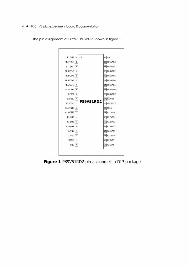
The pin assignment of P89V51RD2BN is shown in figure 1.
P89V51RD2
1
2
3
40
39
38
37
36
35
4
5
6
7
8
9
10
11
12
34
33
32
31
30
29
13
14
28
27
15
16
26
25
17
18
24
23
19
20
22
21
P1.0/T2
P1.1/T2EX
P1.2/ECI
P1.3/CEX0
P1.4/CEX1
P1.5/CEX2
P1.6/CEX3
P17/CEX4
RESET
P3.0/RxD
P3.1/TxD
P3.2/INT0
P3.3/INT1
P3.4/T0
P3.5/T1
P3.6/WR
P3.7/RD
XTAL2
XTAL1
GND
+Vcc
P0.0/AD0
P0.1/AD1
P0.2/AD2
P0.3/AD3
P0.4/AD4
P0.5/AD5
P0.6/AD6
P0.7/AD7
EA/Vpp
ALE/PROG
PSEN
P2.7/A15
P2.6/A14
P2.5/A13
P2.4/A12
P2.3/A11
P2.2/A10
P2.1/A9
P2.0/A8
Figure 1 P89V51RD2 pin assignmet in DIP package

NX-51 V2 plus experiment board Documentationl5
Table 1-1 Summary of pin function of P89V51RD2BN microcontroller
PinPin name Type Description
39-32P0.0-P0.7 Input/Output Port 0 is an 8-bit open drain bi-directional I/O port. Port 0 pins that have ‘1’s written to them float, and in thisstate can be used as high-impedance inputs. Port 0 is also the multiplexed low-order address and data bus duringaccesses to external code and data memory. In this application, it uses strong internal pull-ups when transitioningto ‘1’s. Port 0 also receives the code bytes during the external host mode programming, and outputs the codebytes during the external host mode verification. External pull-ups are required during program verification or as ageneral purpose I/O port.
40Vcc Input Supply +5V
20GND Input Ground
1-8P1.0-P1.7 Input/Output Port 1 is an 8-bit bi-directional I/O port with internal pull-ups. As inputs, Port 1 pins that are externally pulled LOWwill source current (IIL) because of the internal pull-ups. P1.5, P1.6, P1.7 have high current drive of 16 mA. Port 1also receives the low-order address bytes during the external host mode programming and verification.- Timer 2 adn SPI (Serial Peripheral Interface) port function as :
T2 (P1.0 : pin 1) External count input to Timer/Counter 2 or Clock-out from Timer/Counter 2T2EX (P1.1 : pin 2) Timer/Counter 2 capture/reload trigger and direction controlECI (P1.2 : pin 3) External clock input. This signal is the external clock input for the PCA.CEX0 (P1.3 : pin 4) Capture/compare external I/O for PCA Module 0.CEX1/SS (P1.4 : pin 5) Capture/compare external I/O for PCA Module 1 and Slave Select in SPICEX2/MOSI (P1.5 : pin 6) Capture/compare external I/O for PCA Module 2 and SPI Master Output Slave InputCEX3/MISO (P1.6 : pin 7) Capture/compare external I/O for PCA Module 3 and SPI Master Input Slave OutpuCEX4/SCK (P1.7 : pin 8) Capture/compare external I/O for PCA Module 4 and SPI clock
21-28P2.0-P2.7 Input/Output Port 2 is an 8-bit bi-directional I/O port with internal pull-ups.
10-17P3.0-P3.7 Input/Output
9RESET Input Reset by the external logic "1" at least 2 machine cycle. While the oscillator is running.
30ALE Output ALE is the output signal for latching the low byte of the address during an access toexternal memory.
29PSEN Output PSEN is the read strobe for external program memory. When the device is executing from internal programmemory, PSEN is inactive (HIGH). When the device is executing code from external program memory, PSEN isactivated twice each machine cycle, except that two PSEN activations are skipped during each access to externaldata memory. A forced HIGH-to-LOW input transition on the PSEN pin while the RST input is continually held HIGHfor more than 10 machine cycles will cause the device to enter external host mode programming.- For P89V51RD2 connect this pin to ground, apply logic "1" at P2.7 and apply +5V at EA/Vpp pin.
31EA/Vpp Input EA must be connected to VSS in order to enable the device to fetch code from the external program memory.EA must be strapped to VDD for internal program execution.However, Security lock level 4 will disable EA, and program execution is only possible from internal programmemory. The EA pin can tolerate a high voltage of 12 V.
19XTAL1 Input Input to the inverting oscillator amplifier and input to the internal clock generator circuits.
18XTAL2 Output Output from the inverting oscillator amplifier.
P3.7 with internal pull-up Port 3 is an 8-bit bidirectional I/O port with internal pull-ups. Port 3 pins are pulled HIGHby the internal pull-ups when ‘1’s are written to them and can be used as inputs in this state. As inputs, Port 3 pinsthat are externally pulled LOW will source current (IIL) IIL) because of the internal pull-ups. Port 3 also receivessome control signals and a partial of high-order address bits during the external host mode programming andverification.- Support many special function port as :
RxD (P3.0 : pin 10) serial input portTxD (P3.1 : pin 11) serial output portINT0 (P3.2 : pin 12) external interrupt 0 inputINT1 (P3.3 : pin 13) external interrupt 1 inputT0 (P3.4 : pin 14) external count input to Timer/Counter 0T1 (P3.5 : pin 15) external count input to Timer/Counter 1WR (P3.6 : pin 16) external data memory write strobeRD (P3.7 : pin 17) external data memory read strobe

6lNX-51 V2 plus experiment board Documentation
2. NX-51 V2plus : P89V51RD2 MCS-51 microcontroller experiment board
2.1 Features :l Support Philips’s P89C(V)51Rx2 (P89V51RD2BN on-board) Clock 11.0592MHz
l In -system programming via serial port
l Select PROGRAM with a switch
l On-board 16x2 LCD module
l 8-LEDs and 2-digit LED 7 segments
l Piezo speaker
l 4x3 Matrix switch
l Relay and stepper motor driver circuit
l DS1820 1-wire Temperature IC
l DS1307 Real-time clock IC
l 2-Interrupt switch l RS-232 interface
l PCF8574A I/O expander IC
l 24C16 SEEPROM on-board
l D/A converter R-2R ladder
l I2C bus-based ADC 4 ch. and 1 DAC by PCF8591
l Connecter for Timer2 and PCA module
l Port1 can select 2 mode : P1 or Timer2 and PCA
l Use with DC adapter+12V 500-800mA
l Polarity protection circuit

NX-51 V2 plus experiment board Documentationl7
+5V
R14-R21220x8
LED8LED7LED6LED5LED4LED3LED2LED1
40
+5V C30.1/50
9RST
11
10
P3.1
RxD P3.0
+5V
1213
INT0\INT1\
P3.2P3.3
14T0 P3.4
1 2 3
4 5 6
* 0 #
7 8 9
P2.0
P2.1
P2.2
P2.3
21
22
23
24
P2.4P2.5P2.6
252627
R53
R54R53-R5510k x3
+5VINT0INT1GND
K11INTERRUPT
INPUT+5VT0
+5V
GND
K10TIMER0INPUT
S17 S18
S5-S16Keypad
4x3
R49
R50
R52
R49-R524k7 x4
3233343536373839
P0.7P0.6P0.5P0.4P0.3P0.2P0.1P0.0
98765432
D7D6D5D4D3D2D1D0
Q7Q6Q5Q4Q3Q2Q1Q0
1112131415161718
1 10 19
+5V
20
98765432
D7
D6D5D4D3D2D1D0
Q7
Q6Q5Q4Q3Q2Q1Q0
1213141516171819
11 1 10
+5V
20
5
64
14 13 12 11 10 9 8 7D7 D6 D5 D4 D3 D2 D1 D0
E
R/W
RS
+5V
23
1
R510k x8
C40.1/50V
VR110k
R6-R13510x8
DSP1
DSP1-DSP2 LED 7 SEGMENTS COMMON CATHODE
gfedcba
dpDSP2
P1.4P1.3
P1.2
54
3
DRIVER selectDSP2 common line
DSP1
5 12
IC5ULN2003
+12V (+Vmotor)
8
PHASE1PHASE2
916
23
11514134 PHASE3
PHASE4
321
A2A1A0
8
1514
SDA
SCL
+5V
16
P7P6P5P4P3
P1P0
12111097654
P2
+5V
+5V
+5V
18 19
C733pF
C633pF
XTAL111.0592MHz
1 2
C1015pF
C915pF
XTAL232.768kHz
3
SDA
SCLA2A1A0
+V
+VrefAoutI1I2I3I4AG
13 4 3 2 1 15
14
16109765
8
IC2P89C51RD
IC374HC541
DSP3LCD 16x2
IC474HC573
+5V
C50.1/50
K2STEPPER MOTOR
OUTPUT
IC6PCF8574A
S3DIP SW. x4
D3D2D1D0
R27
R28
R29
R30
LED9
LED10
LED11
LED12
D3D2D1D0
R27-R30220 x4
IC8PCF8591
C80.1/50
K5ANALOGOUTPUT
K4ANALOGINPUT
7
5 6
SDA
SCL
+B4
P1.0
P1.1
1
2
SDA
SCL
IC9DS1307
BATT13V
K12SERIAL PORT
20
P0.7P0.6P0.5P0.4P0.3P0.2P0.1P0.0
P0.7P0.6P0.5P0.4P0.3P0.2P0.1P0.0
com com
1617
P3.6P3.7
R3820k
R3720k
R4510k
R3620k
R4610k
R3520k
R4410k
R3420k
R4310k
R3320k
R4210k
R3220k
R4110k
R3120k
R4010k
R3920k
K8ANALOGOUTPUT
1 10 11
+5V
20
C110.1/50
98765432
Q7Q6Q5Q4Q3Q2Q1Q0
1213141516171819
D7D6D5D4D3D2D1D0
P3.515
P0.7P0.6P0.5P0.4P0.3P0.2P0.1P0.0
D7
D6
D5
D4
D3
D2
D1
D0
R-2R select
+
-
+5V
K3I2C BUS
+5VSDASCLGND
DQ4DQ3DQ2DQ1DQ0
DQ4
DQ3DQ2DQ1DQ0
+V RY1RELAY12V
K1RELAY
OUTPUT
NO
C
NC
JP8DRIVER ENABLE
IC1074HC573
SP1PIEZO
10
98
7
3
1
5
4
16 2
+5V
6 15C19
IC13MAX232
C18
C16
C15
TxD
C17
R231k
R221k
Q2BC557 Q1
BC557
+5V
R24-R254k7
+5V
R26/14k7 x8
R26/24k7 x8
K9DC INPUT
IC127805
+5VC12
220/25
C140.1/50
+-
C130.1/50
~
~
+
-
BD11N4001 x4
R48220
LED13POWER
R55
R51
23
78
1
45
6
+5V T2 T2EX
GND
7P1.68P1.7
K6TIMER2 PORT
321
A2A1A0
4
56
SDA
SCL
8
WP7IC7
24C/LC16
+5V
31 EA/Vpp
C15-C1910/50V
CLK8
R474k7
12
R22390
PSEN29
28 P2.7
DQ5
+5V+5V
+5V
IC14DS1820
23
+5V
1
3
5
12
76
84
R1100k
C12.2/50V
IC1555
C20.01/50V
LED1RUN
LED2PGM
R2510
R3220
S1RESET
S2MODE
R41.5k
P1.5 6
ECI (PCA)
CEX2 3 4 ECI
K7PCA PORT
R564.7k
+-
GND
4321
+5V
VR2-VR510k x4
JP4-JP7ADC test
SDA
SCL
T2
T2EX
JP3
JP2
JP1
Figure 2 NX-51 V2 plus experiment board schematic diagram
3. Flash Magic softwareThe ISP software that use with NX-51 V2 plus board is Flash Magic V2.0 or higher. You
can download the latest version at www.esacademy.com. After downloaded, install toyour computer that have Windows 98SE or higher. Before using this software, must connectthe experiment board with computer’s serial port. The figure 3 shows the main window ofFlash Magic software.
The main window has 5 setting boxes. Each box has number indentify. This numbermeans step of operation. You must set in the order from box 1 to 5. Start by select theinterface COM port, select the eraseing memory, select the target file, select some optionand click the start button. in the last. However you can select the operation via menubar. Read mre information in the PDF file manual in same folder that contain this software.

8lNX-51 V2 plus experiment board Documentation
รูปท่ี 1-5 หนาตางหลักของโปรแกรม FlashMagic
4. How to use Flash Magic with NX-51 v2 plus experimentboard
(1) Connect the experiment board with RS-232 serial port by serial cable. If yourcomputer has only USB port, do not worry. You can use USB to serial port adapter. Werecommend UCON-232 board. See more detail at www.inexglobal.com.
(2) Make sure not have any software that operate with Computer’s serail port.
(3) Because using P89V51RD2BN on this experiment board, the MODE switch doesnot use. You must set the switch into RUN mode only. A green LED will on.
(4) Run the Flash Magic software. The title page will appear in a moment. After thatthe main window will appear and has the message Attempting to connect... at status barin the bottom of window. If the error dialogue box in the figure 4 appears, it means theexperiment board cannot interface with flash Magic software. Click the Cancel buttonto continue.
Figure 3 The main window of Flash Magic software in P89V51RD2 selection

NX-51 V2 plus experiment board Documentationl9
(5) At the Setting Box 1, select the COM port interface, Baudrate as 9600 and selectMicrocontroller number to 89V51RD2.
(6) At the Setting BOX 2, check the Erase all flash box for erasing all flash programmemory.
(6) Select the target HEX file in the Setting Box 3.
Figure 4 The error dialogue box about interface between P89V51RD2microcontroller and Flash Magic software

10lNX-51 V2 plus experiment board Documentation
(7) In the Setting Box 4, user can select any parameter or not select. Howeversuggess to select at the Verify after programming.
For P89V51RD2 microcontroller that bundled with NX-51 V2 plus experimentboard will pre-programmed the 6 clks/cycle mode from manufacturer. Thus, all timing inyour code must adjust to relate with 6 clks/cycle. It means the speed will faster 2 timecompare the 8051 original. P89V51RD2 cannot select back to 12 clks/cycle via ISPprocudure. If you need to set back must use the Parallel programmer such as ALL-11 fromHi-Lo system.
(8) Select all 3 P1 SELECTION jumpers to suitable circuit.
(9) Click Start button in the Setting Box 5 to start the downloading.
The warning dialogue box in the figure 5 will apeear. The box infrom you toreset the experiment board to enter the ISP mode.
Apply the supply voltage in this moment or if the board is applied the supplyvoltage before, press RESET switch on the experiment board instead. Do not click Cancelbutton. After that that dialogue box will close automatically and enter to ISP mode withthe download process will happen suddenly.
(10) After the downloading is finished, press RESET switch on the experiment boardagin to run the program.

NX-51 V2 plus experiment board Documentationl11
Figure 5 The Reset Device dialogue appear at the middle of main window toinform user to reset the hardware for entering ISP mode.
5. The MCS-51 CD-ROM informationThe CD-ROM that bundled with NX-51 V2 plus experiemnt board is contained many
software and experiment codes.
5.1 Code for Experiment folder : contains all experiment, for P89V51RD2experiment enter to folder V51Lab_sourcecode. You will found
5.1.1 INCLUDE folder - contains all header and library that use in allexperiment
5.1.2 Lxxxx - xxxx means number of experiment file. Start from 0101 to2601. All C project file of all experiment developed with Rkit-51 by Raisonance. You candownload evaluation version free of charge at www.raisonance.com. All experiment cancompile under the evaluation version.
5.2 Software folder : contains the variety of software tool for develope MCS-51 microcontroller. The softwares that use in all experiment code from 5.1.2 are :
5.2.1 RKIT51 BN733 folder - contains Rkit-51 in evaluation version.
5.2.2 FlashMagic 2.xx - contains the Flash Magic V2.5 or higer.

12lNX-51 V2 plus experiment board Documentation


![NX post processor [NX CAM]](https://static.documents.pub/doc/80x56/588910c81a28ab4a5c8b59e9/nx-post-processor-nx-cam.jpg)

