1. General description
The NX3DV642 is a high-speed triple-pole double-throw differential signal switch. The device is optimized for switching between two MIPI devices, such as cameras or LCD displays and on-board multimedia application processors.
The NX3DV642 is compatible with the requirements of Mobile Industry Processor Interface (MIPI). The low capacitance design allows the NX3DV642 to switch signals that exceed 500 MHz in frequency
2. Features and benefits
Supply voltage range from 2.65 V to 4.3 V
7.5 typical ON resistance
8.4 pF typical ON capacitance
950 MHz typical bandwidth or data frequency
Low crosstalk of 55 dB at 100 MHz
Break-before-make switching
ESD protection:
HBM JESD22-A114F Class 2 exceeds 2000 V
CDM AEC-Q100-011 revision B exceeds 1000 V
HBM exceeds 12000 V for power to GND protection
Latch-up performance exceeds 100 mA per JESD 78 Class II Level A
Specified from 40 C to +85 C
3. Applications
Dual camera applications for cell phones
Dual LCD applications for cell phones, digital camera displays and viewfinders
4. Ordering information
NX3DV6423-lane high-speed MIPI compatible switchRev. 1 — 20 August 2012 Product data sheet
Table 1. Ordering information
Type number Package
Temperature range Name Description Version
NX3DV642GU 40 C to +85 C XQFN24 plastic, extremely thin quad flat package; no leads; 24 terminals; body 2.5 x 3.4 x 0.5 mm
SOT1310-1
NXP Semiconductors NX3DV6423-lane high-speed MIPI compatible switch
5. Marking
6. Functional diagram
Table 2. Marking
Type number Marking code
NX3DV642GU 3DV642
Fig 1. Logic symbol
17
221
CLK1+CLK+
CLK2+
16
232
CLK1-CLK-
CLK2-
15
203
1D1+1D+
1D2+
14
214
1D1-1D-
1D2-
13
195
2D1+2D+
2D2+
12
186
2D1-2D-
8OE
CONTROLLOGIC
2D2-
aaa-002567
11S
Fig 2. Application block diagram
MAP PROCESSORDD C
aaa-002568
LCD 2DD C
LCD 1DD C
NX3DV642
MAP PROCESSORDC D
CAMERA 2DC D
CAMERA 1DD C
NX3DV642
NX3DV642 All information provided in this document is subject to legal disclaimers. © NXP B.V. 2012. All rights reserved.
Product data sheet Rev. 1 — 20 August 2012 2 of 16
NXP Semiconductors NX3DV6423-lane high-speed MIPI compatible switch
7. Pinning information
7.1 Pinning
7.2 Pin description
Fig 3. Pin configuration SOT1310-1 (XQFN24)
terminal 1index area
aaa-002569
NX3DV642
Transparent top view
1
2
3
4
5
6
18
17
16
15
14
13
2D2-
CLK1+
CLK1-
1D1+
1D1-
2D1+
CLK+n.
c.
OE
GN
D
VC
C S
2D1-
n.c.
CLK
2-
CLK
2+
1D2-
1D2+
2D2+
CLK-
1D+
1D-
2D+
2D-
987 10 11 12
222324 21 20 19
Table 3. Pin description
Symbol Pin Description
CLK+, CLK 1, 2 common output or input clock path
1D+, 1D 3, 4 common output or input data path 1D
2D+, 2D 5, 6 common output or input data path 2D
n.c. 7, 24 not connected
OE 8 output enable input (active LOW)
GND 9 ground (0 V)
VCC 10 supply voltage
S 11 select input
2D1+, 2D1 13, 12 independent input or output data path 2D1
1D1+, 1D1 15, 14 independent input or output data path 1D1
CLK1+, CLK1 17, 16 independent input or output clock path CLK1
2D2+, 2D2 19, 18 independent input or output data path 2D2
1D2+, 1D2 20, 21 independent input or output data path 1D2
CLK2+, CLK2 22, 23 independent input or output clock path CLK2
NX3DV642 All information provided in this document is subject to legal disclaimers. © NXP B.V. 2012. All rights reserved.
Product data sheet Rev. 1 — 20 August 2012 3 of 16
NXP Semiconductors NX3DV6423-lane high-speed MIPI compatible switch
8. Functional description
[1] H = HIGH voltage level; L = LOW voltage level; X = don’t care. (n = + or )
9. Limiting values
[1] The minimum input voltage rating may be exceeded if the input current rating is observed.
10. Recommended operating conditions
[1] To avoid sinking GND current from terminals CLKn, 1Dn and 2Dn when switch current flows in terminals CLK1n, CLK2n, 1D1n 1D2n, 2D1n and 2D2n (n = + or ), the voltage drop across the bidirectional switch must not exceed 0.4 V. If the switch current flows into terminals CLKn, 1Dn and 2Dn, no GND current flows from terminals CLK1n, CLK2n, 1D1n 1D2n, 2D1n and 2D2n. In this case, there is no limit for the voltage drop across the switch.
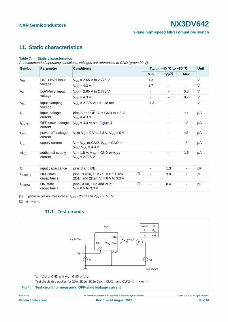
Table 4. Function table[1]
Input Channel on
S OE
L L CLKn, 1Dn, 2Dn = CLK1n, 1D1n, 2D1n
H L CLKn, 1Dn, 2Dn = CLK2n, 1D2n, 2D2n
X H switch off
Table 5. Limiting valuesIn accordance with the Absolute Maximum Rating System (IEC 60134). Voltages are referenced to GND (ground = 0 V).
Symbol Parameter Conditions Min Max Unit
VCC supply voltage 0.5 +5.5 V
VI input voltage pins S and OE [1] 0.5 +5.5 V
VSW switch voltage 0.5 +5.5 V
IIK input clamping current VI < 0.5 V 50 - mA
ISK switch clamping current VI < 0.5 V 50 +50 mA
ISW switch current 100 +100 mA
ICC supply current - +50 mA
Tstg storage temperature 65 +150 C
Ptot total power dissipation Tamb = 40 C to +85 C - 533 mW
Table 6. Recommended operating conditions
Symbol Parameter Conditions Min Max Unit
VCC supply voltage 2.65 4.3 V
VI input voltage pins S and OE 0 4.3 V
VSW switch voltage [1] 0 4.5 V
Tamb ambient temperature 40 +85 C
NX3DV642 All information provided in this document is subject to legal disclaimers. © NXP B.V. 2012. All rights reserved.
Product data sheet Rev. 1 — 20 August 2012 4 of 16
NXP Semiconductors NX3DV6423-lane high-speed MIPI compatible switch
11. Static characteristics
[1] Typical values are measured at Tamb = 25 C and VCC = 2.775 V.
[2] n = + or .
11.1 Test circuits
Table 7. Static characteristicsAt recommended operating conditions; voltages are referenced to GND (ground 0 V).
Symbol Parameter Conditions Tamb = 40 C to +85 C Unit
Min Typ[1] Max
VIH HIGH-level input voltage
VCC = 2.65 V to 2.775 V 1.3 - - V
VCC = 4.3 V 1.7 - - V
VIL LOW-level input voltage
VCC = 2.65 V to 2.775 V - - 0.5 V
VCC = 4.3 V - - 0.7 V
VIK input clamping voltage
VCC = 2.775 V; II = 18 mA 1.2 - - V
II input leakage current
pins S and OE; VI = GND to 4.3 V; VCC = 4.3 V
- - 1 A
IS(OFF) OFF-state leakage current
VCC = 4.3 V; see Figure 4 - - 2 A
IOFF power-off leakage current
VI or VO = 0 V to 4.3 V; VCC = 0 V - - 2 A
ICC supply current VI = VCC or GND; VSW = GND or VCC; VCC = 4.3 V
- - 2 A
ICC additional supply current
VI = 1.8 V; VSW = GND or VCC; VCC = 2.775 V
- - 1.5 A
CI input capacitance pins S and OE - 1.3 - pF
CS(OFF) OFF-state capacitance
pins CLK1n, CLK2n, 1D1n 1D2n, 2D1n and 2D2n; VI = 0 V to 3.3 V
[2] - 3.0 - pF
CS(ON) ON-state capacitance
pins CLKn, 1Dn and 2Dn; VI = 0 V to 3.3 V
[2] - 8.4 - pF
VI = VCC or GND and VO = GND or VCC.
Test circuit also applies for 2Dn, 2D1n, 2D2n CLKn, CLK1n and CLK2n (n = + or ).
Fig 4. Test circuit for measuring OFF-state leakage current
S
1Dn
1D1nVIL or VIH
VIH
VCC switch1
2 VIH
VIL
S
VI
aaa-002570
1D2nswitch
GNDOE
1
2
VO
IS
NX3DV642 All information provided in this document is subject to legal disclaimers. © NXP B.V. 2012. All rights reserved.
Product data sheet Rev. 1 — 20 August 2012 5 of 16
NXP Semiconductors NX3DV6423-lane high-speed MIPI compatible switch
11.2 ON resistance
[1] Typical values are measured at Tamb = 25 C.
[2] Measured at identical VCC, temperature and input voltage.
11.3 ON resistance test circuit and graphs
Table 8. ON resistanceAt recommended operating conditions; voltages are referenced to GND (ground = 0 V).
Symbol Parameter Conditions 40 C to +85 C Unit
Min Typ[1] Max
low speed mode
RON ON resistance VI = 1.2 V; ISW = 10 mA; see Figure 5
VCC = 2.65 V - 7.5 14
RON ON resistance mismatch between channels
VI = 1.2 V; ISW = 10 mA [2]
VCC = 2.65 V - 0.65 -
High speed mode
RON ON resistance VI = 0.1 V; ISW = 10 mA; see Figure 5
VCC = 2.65 V - 5.5 9.5
RON ON resistance mismatch between channels
VI = 0.1 V; ISW = 10 mA [2]
VCC = 2.65 V - 0.65 -
RON = VSW / ISW.
Test circuit also applies for 2Dn, 2D1n, 2D2n CLKn, CLK1n and CLK2n (n = + or ).
Fig 5. Test circuit for measuring ON resistance
S
1Dn
1D1nVIL or VIH
VIL
VCCswitch
1
2 VIH
VIL
S
VI
aaa-002571
1D2nswitch
GNDOE
1
2
V
VSW
ISW
NX3DV642 All information provided in this document is subject to legal disclaimers. © NXP B.V. 2012. All rights reserved.
Product data sheet Rev. 1 — 20 August 2012 6 of 16
NXP Semiconductors NX3DV6423-lane high-speed MIPI compatible switch
12. Dynamic characteristics
[1] Typical values are measured at Tamb = 25 C, CL = 5 pF and VCC = 2.775 V.
[2] n = + or .
[3] tpd is the same as tPLH and tPHL.
ten is the same as tPZH
tdis is the same as tPHZ
[4] Guaranteed by design.
12.1 Waveform and test circuits
Table 9. Dynamic characteristicsAt recommended operating conditions; voltages are referenced to GND (ground = 0 V); for load circuit see Figure 9.
Symbol Parameter Conditions Tamb = 40 C to +85 C Unit
Min Typ[1] Max
tpd propagation delay CLKn to CLK1n or CLK2n; 1Dn to 1D1n or 1D2n or 2Dn to 2D1n or 2D2n; see Figure 6
[2][3][4]
VCC = 2.775 V - 0.25 - ns
ten enable time S or OE to CLKn, 1Dn or 2Dn; see Figure 7 [2][3]
VCC = 2.65 V to 2.775 V - 13.5 37 ns
tdis disable time S or OE to CLKn, 1Dn or 2Dn; see Figure 7 [2][3]
VCC = 2.65 V to 2.775 V - 5.5 27 ns
tb-m break-before-make time see Figure 8 [4]
VCC = 2.65 V to 2.775 V 3 7 - ns
tsk(p) pulse skew time VCC = 2.65 V to 2.775 V; VSW = 0.2 V (p-p) [4] - 10 - ps
tsk(o) output skew time VCC = 2.65 V to 2.775 V; VSW = 0.2 V (p-p) [4] - 15 - ps
tsk(pr) process skew time VCC = 2.65 V to 2.775 V; VSW = 0.2 V (p-p) [4] - 40 - ps
Logic levels: VOL and VOH are typical output voltage levels that occur with the output load.
tr = tf 500 ps.
Fig 6. The data input to output propagation delay times
aaa-001359
tPHLtPLH
50%
50%input
400 mV
GND
VOH
VOL
output
NX3DV642 All information provided in this document is subject to legal disclaimers. © NXP B.V. 2012. All rights reserved.
Product data sheet Rev. 1 — 20 August 2012 7 of 16
NXP Semiconductors NX3DV6423-lane high-speed MIPI compatible switch
Measurement points are given in Table 10.
Logic level: VOH and VOLare typical output voltage levels that occur with the output load.
Fig 7. Enable and disable times
aaa-002572
tPHZ
switchdisabled
switchenabled
switchenabled
outputHIGH to OFFOFF to HIGH
S, OE input
VOH
GND
GND
VI
tPZH
VM
VX VX
Table 10. Measurement points
Supply voltage Input Output
VCC VM VI VX
2.65 V to 2.775 V 0.5VCC VCC 0.9VOH
a. Test circuit.
b. Input and output measurement points
Test circuit also applies for 2Dn, 2D1n, 2D2n CLKn, CLK1n and CLK2n (n = + or ).
Fig 8. Test circuit for measuring break-before-make timing
aaa-002573
RL
S
GND
1Dn
1D1n
1D2n
VCC
VI CLG V VO VEXT = 1.2 V
VIL
OE
001aag572
VI
tb-m
VO
0.9VO0.9VO
0.5VI
NX3DV642 All information provided in this document is subject to legal disclaimers. © NXP B.V. 2012. All rights reserved.
Product data sheet Rev. 1 — 20 August 2012 8 of 16
NXP Semiconductors NX3DV6423-lane high-speed MIPI compatible switch
12.2 Additional dynamic characteristics
[1] fi is biased at 0.5VCC.
Test circuit also applies for 2Dn, 2D1n, 2D2n CLKn, CLK1n and CLK2n (n = + or ).
Test data is given in Table 11.
Definitions test circuit:
RT = Termination resistance (should be equal to output impedance Zo of the pulse generator).
RL = Load resistance.
CL = Load capacitance including jig and probe capacitance.
VEXT = External voltage for measuring switching times.
VI may be connected to S or OE.
Fig 9. Test circuit for measuring switching times
aaa-002574
RL
S
GND
1Dn
1D1n
1D2n
VCC
VI CLG VEXT = 1.2 V
VIL
OE
Table 11. Test data
Supply voltage Input Load
VCC VI tr, tf CL RL
2.65 V to 2.775 V VCC 2.5 ns 5 pF 50
Table 12. Additional dynamic characteristicsAt recommended operating conditions; voltages are referenced to GND (ground = 0 V); VI = GND or VCC (unless otherwise specified); tr = tf 2.5 ns.
Symbol Parameter Conditions Tamb = 25 C Unit
Min Typ Max
f(3dB) 3 dB frequency response
RL = 50 ; see Figure 10 [1]
CL = 0 pF; VCC = 2.775 V - 950 - MHz
iso isolation (OFF-state) fi = 100 MHz; RL = 50 ; see Figure 11 [1]
VCC = 2.775 V - 35 - dB
Xtalk crosstalk between switches; fi = 100 MHz; RL = 50 ; see Figure 12
[1]
VCC = 2.775 V - 55 - dB
NX3DV642 All information provided in this document is subject to legal disclaimers. © NXP B.V. 2012. All rights reserved.
Product data sheet Rev. 1 — 20 August 2012 9 of 16
NXP Semiconductors NX3DV6423-lane high-speed MIPI compatible switch
12.3 Test circuits
Adjust fi voltage to obtain 0 dBm level at output. Increase fi frequency until dB meter reads 3 dB.
Test circuit also applies for 2Dn, 2D1n, 2D2n CLKn, CLK1n and CLK2n (n = + or ).
Fig 10. Test circuit for measuring the frequency response when channel is in ON-state
S
1Dn
1D1nVIL or VIH
VIL
VCC 0.5 VCC switch1
2 VIH
VIL
S
fi
aaa-002575
1D2nswitch
GNDOE
1
2
CL
RL
dB
Adjust fi voltage to obtain 0 dBm level at input.
Test circuit also applies for 2Dn, 2D1n, 2D2n CLKn, CLK1n and CLK2n (n = + or ).
Fig 11. Test circuit for measuring isolation (OFF-state)
S
1Dn
1D1nVIL or VIH
VIH
VCC 0.5 VCC switch1
2 VIL
VIH
S
fi
aaa-002576
1D2nswitch
GNDOE
1
2
RL
0.5 VCC
RL
dB
NX3DV642 All information provided in this document is subject to legal disclaimers. © NXP B.V. 2012. All rights reserved.
Product data sheet Rev. 1 — 20 August 2012 10 of 16
NXP Semiconductors NX3DV6423-lane high-speed MIPI compatible switch
20 log10 (VO2 / VO1) or 20 log10 (VO1 / VO2).
Fig 12. Test circuit for measuring crosstalk between switches
V
aaa-002577
CHANNELOFF
CLK-, nD-
S 0.5 VCC
RL
Ri50 Ω VO2
CLK2- or nD2-
V
CHANNELON
CLK+, nD+
VIL
0.5 VCC
RL
50 Ωfi VO1
CLK1+ or nD1+
NX3DV642 All information provided in this document is subject to legal disclaimers. © NXP B.V. 2012. All rights reserved.
Product data sheet Rev. 1 — 20 August 2012 11 of 16
NXP Semiconductors NX3DV6423-lane high-speed MIPI compatible switch
13. Package outline
Fig 13. Package outline SOT1310-1 (XQFN24)
ReferencesOutlineversion
Europeanprojection Issue date
IEC JEDEC JEITA
SOT1310-1 MO-288
sot1310-1_po
11-07-1911-08-18
Unit
mmmaxnommin
0.5 0.05 2.6 3.52.0 0.40 0.10
A
Dimensions
Note1. Plastic or metal protrusions of 0.075 mm maximum per side are not included
XQFN24: plastic, extremely thin quad flat package; no leads; 24 terminals; body 2.5 x 3.4 x 0.5 mm SOT1310-1
A1 b
0.250.127 2.5 3.4 0.40.20
A3 D E e
0.05
e1
2.0
e2 L L1
0.50
v w
0.050.45 0.55
y y1
0.00 2.4 3.30.15 0.35 0.450.05
0 2 mm
scale
D
E
B
terminal 1index area
A
C
yCy1
X
detail X
A3
A1A
L
6
1
L1
24 19
18
13
e2
e
1/2 e
1/2 e
e1
AC Bvw C
b
e
127
NX3DV642 All information provided in this document is subject to legal disclaimers. © NXP B.V. 2012. All rights reserved.
Product data sheet Rev. 1 — 20 August 2012 12 of 16
NXP Semiconductors NX3DV6423-lane high-speed MIPI compatible switch
14. Abbreviations
15. Revision history
Table 13. Abbreviations
Acronym Description
CDM Charged Device Model
CMOS Complementary Metal-Oxide Semiconductor
ESD ElectroStatic Discharge
HBM Human Body Model
MM Machine Model
TTL Transistor-Transistor Logic
Table 14. Revision history
Document ID Release date Data sheet status Change notice Supersedes
NX3DV642 v.1 20120820 Product data sheet - -
NX3DV642 All information provided in this document is subject to legal disclaimers. © NXP B.V. 2012. All rights reserved.
Product data sheet Rev. 1 — 20 August 2012 13 of 16
NXP Semiconductors NX3DV6423-lane high-speed MIPI compatible switch
16. Legal information
16.1 Data sheet status
[1] Please consult the most recently issued document before initiating or completing a design.
[2] The term ‘short data sheet’ is explained in section “Definitions”.
[3] The product status of device(s) described in this document may have changed since this document was published and may differ in case of multiple devices. The latest product status information is available on the Internet at URL http://www.nxp.com.
16.2 Definitions
Draft — The document is a draft version only. The content is still under internal review and subject to formal approval, which may result in modifications or additions. NXP Semiconductors does not give any representations or warranties as to the accuracy or completeness of information included herein and shall have no liability for the consequences of use of such information.
Short data sheet — A short data sheet is an extract from a full data sheet with the same product type number(s) and title. A short data sheet is intended for quick reference only and should not be relied upon to contain detailed and full information. For detailed and full information see the relevant full data sheet, which is available on request via the local NXP Semiconductors sales office. In case of any inconsistency or conflict with the short data sheet, the full data sheet shall prevail.
Product specification — The information and data provided in a Product data sheet shall define the specification of the product as agreed between NXP Semiconductors and its customer, unless NXP Semiconductors and customer have explicitly agreed otherwise in writing. In no event however, shall an agreement be valid in which the NXP Semiconductors product is deemed to offer functions and qualities beyond those described in the Product data sheet.
16.3 Disclaimers
Limited warranty and liability — Information in this document is believed to be accurate and reliable. However, NXP Semiconductors does not give any representations or warranties, expressed or implied, as to the accuracy or completeness of such information and shall have no liability for the consequences of use of such information. NXP Semiconductors takes no responsibility for the content in this document if provided by an information source outside of NXP Semiconductors.
In no event shall NXP Semiconductors be liable for any indirect, incidental, punitive, special or consequential damages (including - without limitation - lost profits, lost savings, business interruption, costs related to the removal or replacement of any products or rework charges) whether or not such damages are based on tort (including negligence), warranty, breach of contract or any other legal theory.
Notwithstanding any damages that customer might incur for any reason whatsoever, NXP Semiconductors’ aggregate and cumulative liability towards customer for the products described herein shall be limited in accordance with the Terms and conditions of commercial sale of NXP Semiconductors.
Right to make changes — NXP Semiconductors reserves the right to make changes to information published in this document, including without limitation specifications and product descriptions, at any time and without notice. This document supersedes and replaces all information supplied prior to the publication hereof.
Suitability for use — NXP Semiconductors products are not designed, authorized or warranted to be suitable for use in life support, life-critical or safety-critical systems or equipment, nor in applications where failure or malfunction of an NXP Semiconductors product can reasonably be expected to result in personal injury, death or severe property or environmental damage. NXP Semiconductors and its suppliers accept no liability for inclusion and/or use of NXP Semiconductors products in such equipment or applications and therefore such inclusion and/or use is at the customer’s own risk.
Applications — Applications that are described herein for any of these products are for illustrative purposes only. NXP Semiconductors makes no representation or warranty that such applications will be suitable for the specified use without further testing or modification.
Customers are responsible for the design and operation of their applications and products using NXP Semiconductors products, and NXP Semiconductors accepts no liability for any assistance with applications or customer product design. It is customer’s sole responsibility to determine whether the NXP Semiconductors product is suitable and fit for the customer’s applications and products planned, as well as for the planned application and use of customer’s third party customer(s). Customers should provide appropriate design and operating safeguards to minimize the risks associated with their applications and products.
NXP Semiconductors does not accept any liability related to any default, damage, costs or problem which is based on any weakness or default in the customer’s applications or products, or the application or use by customer’s third party customer(s). Customer is responsible for doing all necessary testing for the customer’s applications and products using NXP Semiconductors products in order to avoid a default of the applications and the products or of the application or use by customer’s third party customer(s). NXP does not accept any liability in this respect.
Limiting values — Stress above one or more limiting values (as defined in the Absolute Maximum Ratings System of IEC 60134) will cause permanent damage to the device. Limiting values are stress ratings only and (proper) operation of the device at these or any other conditions above those given in the Recommended operating conditions section (if present) or the Characteristics sections of this document is not warranted. Constant or repeated exposure to limiting values will permanently and irreversibly affect the quality and reliability of the device.
Terms and conditions of commercial sale — NXP Semiconductors products are sold subject to the general terms and conditions of commercial sale, as published at http://www.nxp.com/profile/terms, unless otherwise agreed in a valid written individual agreement. In case an individual agreement is concluded only the terms and conditions of the respective agreement shall apply. NXP Semiconductors hereby expressly objects to applying the customer’s general terms and conditions with regard to the purchase of NXP Semiconductors products by customer.
No offer to sell or license — Nothing in this document may be interpreted or construed as an offer to sell products that is open for acceptance or the grant, conveyance or implication of any license under any copyrights, patents or other industrial or intellectual property rights.
Document status[1][2] Product status[3] Definition
Objective [short] data sheet Development This document contains data from the objective specification for product development.
Preliminary [short] data sheet Qualification This document contains data from the preliminary specification.
Product [short] data sheet Production This document contains the product specification.
NX3DV642 All information provided in this document is subject to legal disclaimers. © NXP B.V. 2012. All rights reserved.
Product data sheet Rev. 1 — 20 August 2012 14 of 16
NXP Semiconductors NX3DV6423-lane high-speed MIPI compatible switch
Export control — This document as well as the item(s) described herein may be subject to export control regulations. Export might require a prior authorization from competent authorities.
Non-automotive qualified products — Unless this data sheet expressly states that this specific NXP Semiconductors product is automotive qualified, the product is not suitable for automotive use. It is neither qualified nor tested in accordance with automotive testing or application requirements. NXP Semiconductors accepts no liability for inclusion and/or use of non-automotive qualified products in automotive equipment or applications.
In the event that customer uses the product for design-in and use in automotive applications to automotive specifications and standards, customer (a) shall use the product without NXP Semiconductors’ warranty of the product for such automotive applications, use and specifications, and (b) whenever customer uses the product for automotive applications beyond
NXP Semiconductors’ specifications such use shall be solely at customer’s own risk, and (c) customer fully indemnifies NXP Semiconductors for any liability, damages or failed product claims resulting from customer design and use of the product for automotive applications beyond NXP Semiconductors’ standard warranty and NXP Semiconductors’ product specifications.
Translations — A non-English (translated) version of a document is for reference only. The English version shall prevail in case of any discrepancy between the translated and English versions.
16.4 TrademarksNotice: All referenced brands, product names, service names and trademarks are the property of their respective owners.
17. Contact information
For more information, please visit: http://www.nxp.com
For sales office addresses, please send an email to: [email protected]
NX3DV642 All information provided in this document is subject to legal disclaimers. © NXP B.V. 2012. All rights reserved.
Product data sheet Rev. 1 — 20 August 2012 15 of 16
NXP Semiconductors NX3DV6423-lane high-speed MIPI compatible switch
18. Contents
1 General description . . . . . . . . . . . . . . . . . . . . . . 1
2 Features and benefits . . . . . . . . . . . . . . . . . . . . 1
3 Applications . . . . . . . . . . . . . . . . . . . . . . . . . . . . 1
4 Ordering information. . . . . . . . . . . . . . . . . . . . . 1
5 Marking . . . . . . . . . . . . . . . . . . . . . . . . . . . . . . . . 2
6 Functional diagram . . . . . . . . . . . . . . . . . . . . . . 2
7 Pinning information. . . . . . . . . . . . . . . . . . . . . . 37.1 Pinning . . . . . . . . . . . . . . . . . . . . . . . . . . . . . . . 37.2 Pin description . . . . . . . . . . . . . . . . . . . . . . . . . 3
8 Functional description . . . . . . . . . . . . . . . . . . . 4
9 Limiting values. . . . . . . . . . . . . . . . . . . . . . . . . . 4
10 Recommended operating conditions. . . . . . . . 4
11 Static characteristics. . . . . . . . . . . . . . . . . . . . . 511.1 Test circuits . . . . . . . . . . . . . . . . . . . . . . . . . . . . 511.2 ON resistance. . . . . . . . . . . . . . . . . . . . . . . . . . 611.3 ON resistance test circuit and graphs. . . . . . . . 6
12 Dynamic characteristics . . . . . . . . . . . . . . . . . . 712.1 Waveform and test circuits . . . . . . . . . . . . . . . . 712.2 Additional dynamic characteristics . . . . . . . . . . 912.3 Test circuits . . . . . . . . . . . . . . . . . . . . . . . . . . . 10
13 Package outline . . . . . . . . . . . . . . . . . . . . . . . . 12
14 Abbreviations. . . . . . . . . . . . . . . . . . . . . . . . . . 13
15 Revision history. . . . . . . . . . . . . . . . . . . . . . . . 13
16 Legal information. . . . . . . . . . . . . . . . . . . . . . . 1416.1 Data sheet status . . . . . . . . . . . . . . . . . . . . . . 1416.2 Definitions. . . . . . . . . . . . . . . . . . . . . . . . . . . . 1416.3 Disclaimers . . . . . . . . . . . . . . . . . . . . . . . . . . . 1416.4 Trademarks. . . . . . . . . . . . . . . . . . . . . . . . . . . 15
17 Contact information. . . . . . . . . . . . . . . . . . . . . 15
18 Contents . . . . . . . . . . . . . . . . . . . . . . . . . . . . . . 16
© NXP B.V. 2012. All rights reserved.
For more information, please visit: http://www.nxp.comFor sales office addresses, please send an email to: [email protected]
Date of release: 20 August 2012
Document identifier: NX3DV642
Please be aware that important notices concerning this document and the product(s)described herein, have been included in section ‘Legal information’.