AN 1538 Fashion Reference Antenna Design for the UCODE G2XM / G2XL IC Rev. 1.0 — 14 March 2008 Application note 1538 Document information Info Content Keywords UCODE EPC G2, G2XM, G2XL, Reference Design, Antenna Design, Fashion, Aluminum Abstract This application note describes a label antenna design for the UCODE G2XM / G2XL, optimized for fashion applications. This design represents a reference design to demonstrate performance of the NXP UCODE G2XM / G2XL.
Transcript
AN 1538 Fashion Reference Antenna Design for the UCODE G2XM / G2XL IC
Abstract This application note describes a label antenna design for the UCODE G2XM / G2XL, optimized for fashion applications. This design represents a reference design to demonstrate performance of the NXP UCODE G2XM / G2XL.
NXP Semiconductors AN 1538 Reference Label Antenna Design for Fashion Applications
Application note 1538 Rev. 1.0 — 14 March 2008 4 of 21
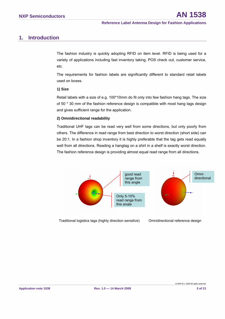
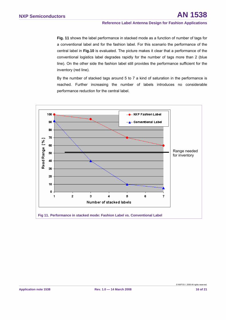
3) Readability in stacked mode
In fashion, tags are often densely stacked e. g. T-shirts on a shelf. Traditional logistics
UHF tags dramatically loose range in these conditions. The NXP fashion reference
design shows consistently strong read range even densely stacked.
2. Technical requirements on a Fashion Design • Region: world wide 860 – 960 MHz; • Read Range 3,5 – 4,5 m • ASIC: G2X (ZIC = 24 – j 195 Ohm @ 915 MHz @ PIC = PIC min ); • Packaging type: direct chip attach; • Performance in presence of additional dielectrics: paper and plastic laminate, apparel
material (from thin shirts to thick jeans) and still operate world wide. • Operates well in typical fashion applications (mobile inventory, smart shelf, POS) • Less orientation sensitivity compared to conventional logistics UHF Tags • Operates in close proximity of other labels • Symmetrical radiation properties according to X and Y axes. • Be competitive with actual benchmark label(s) used for fashion applications
Simulation of densely stacked fashion tags The NXP fashion reference design show significantly better range than conventional tags in stacked mode.
Range needed for inventory
NXP Semiconductors AN 1538 Reference Label Antenna Design for Fashion Applications
Application note 1538 Rev. 1.0 — 14 March 2008 5 of 21
3. Fashion Reference Antenna Design
3.1 Geometry • Dimensions of the design: 50 mm x 30 mm; • Antenna material: copper; thickness 18um; • Substrate material: PET; thickness 50um; • Antenna should be matched to following assembled IC impedance:
(Z ass. IC = 22 – j 147 Ohm @ 915 MHz @ PIC = PIC min );
Cass = 0,3 pF;
Fig 1. Fashion Reference Design
NXP Semiconductors AN 1538 Reference Label Antenna Design for Fashion Applications
Application note 1538 Rev. 1.0 — 14 March 2008 6 of 21
3.2 Design description
To meet all of the above listed requirements a series of special design concepts have been worked out.
The requirement of long read range calls for a utilization of resonance dipole.
To reach the necessary dipole length on a given electrically small label area (50 x 30 mm) on one side and necessary/sufficient radiation in desired directions (the directions, poor for a conventional dipole) on the other side a technique of multiple bending the dipole is used.
To meet the requirements of symmetrical radiation with respect to Y axis the central part of the dipole is placed / shifted close to Y axis. This way however decreases the current in the transverse parts of the dipole (perpendicular to the Y axis) and as a consequence radiation in Y-axis direction. For this reason the central part of the dipole is not exactly symmetric to the Y-axis (see Fig 1).
To make the conjugate-complex matching between the antenna and capacitive ASIC possible, a small inductive loop is utilized.
To ensure the required increased bandwidth of the label the classical conjugate-complex matching technique is set aside. The antenna is tuned in such a manner that a good compromise between a required label performance (Read Range) and a required bandwidth (more than 100 MHz) is made.
The tuning elements are the lengths of both dipole and the loop as well as the way of connection them.
In the present design the loop-dipole connection is created using a mixed magnetic and galvanic coupling.
The performance in a coupling mode is synthesized based on theoretical and experimental investigations as well as based on simulations. The shaping of the loop and dipole as well as changing their geometrical parameters (length, width) were used to tune the antenna for close coupling operation.
Design is optimized for paper laminate!
NXP Semiconductors AN 1538 Reference Label Antenna Design for Fashion Applications
Application note 1538 Rev. 1.0 — 14 March 2008 7 of 21
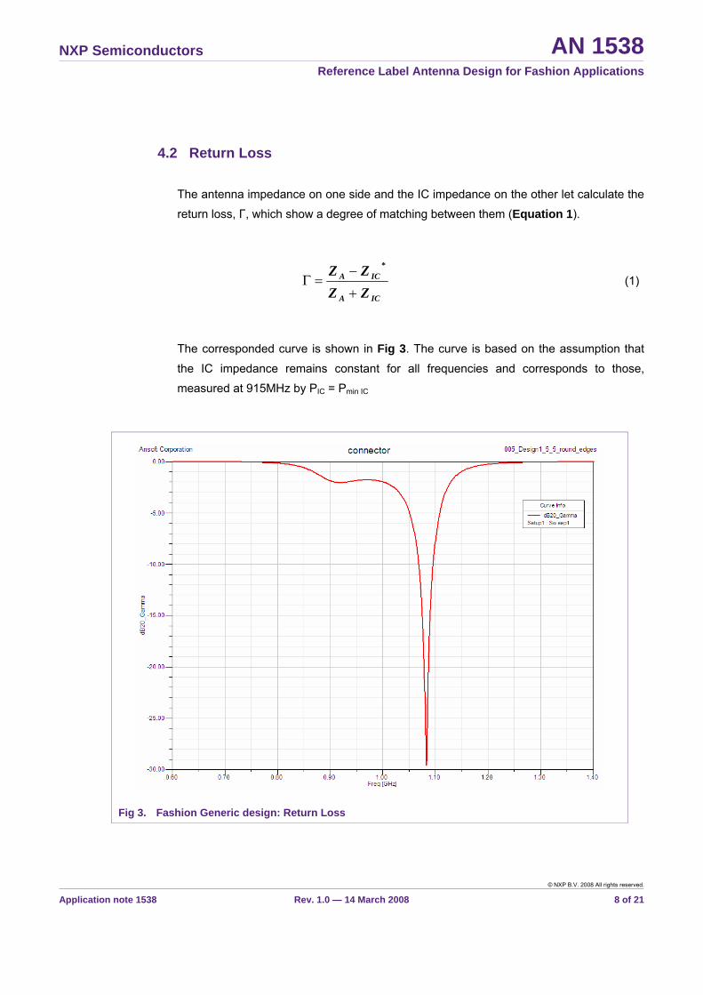
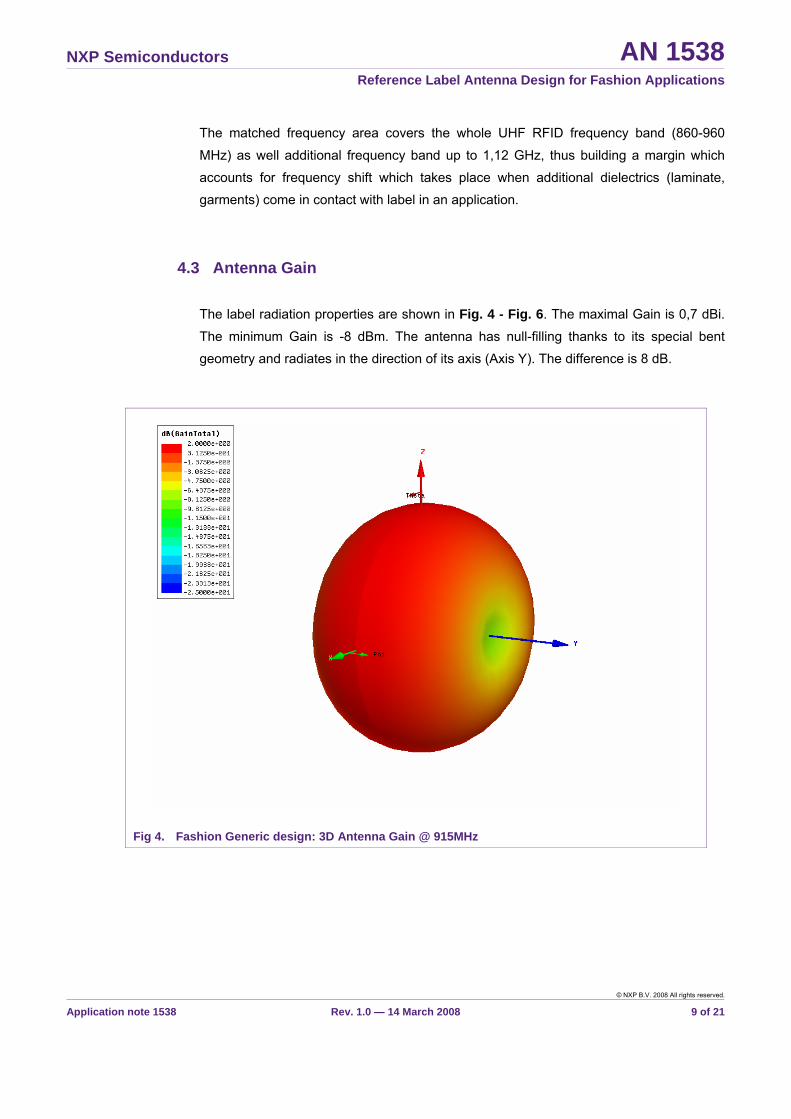
4. HFSS Simulation Results
The following simulations are solved using HFSS, a commercial 3-D finite element method solver for electromagnetic structures used for antenna design and the design of complex RF electronic circuit elements.
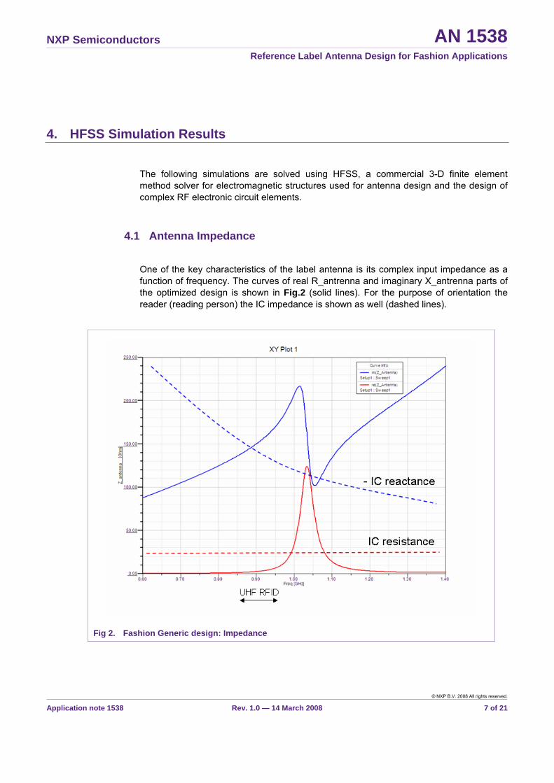
4.1 Antenna Impedance
One of the key characteristics of the label antenna is its complex input impedance as a function of frequency. The curves of real R_antrenna and imaginary X_antrenna parts of the optimized design is shown in Fig.2 (solid lines). For the purpose of orientation the reader (reading person) the IC impedance is shown as well (dashed lines).
Fig 2. Fashion Generic design: Impedance
NXP Semiconductors AN 1538 Reference Label Antenna Design for Fashion Applications
Application note 1538 Rev. 1.0 — 14 March 2008 18 of 21
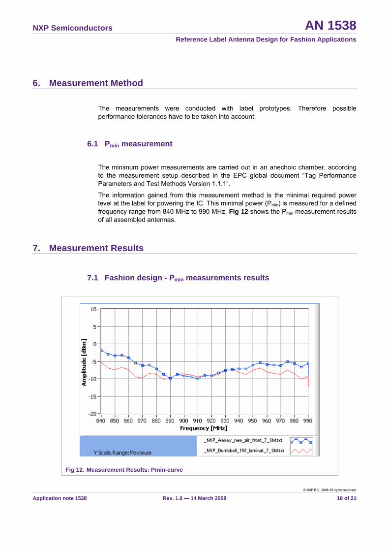
6. Measurement Method
The measurements were conducted with label prototypes. Therefore possible performance tolerances have to be taken into account.
6.1 Pmin measurement
The minimum power measurements are carried out in an anechoic chamber, according to the measurement setup described in the EPC global document “Tag Performance Parameters and Test Methods Version 1.1.1”.
The information gained from this measurement method is the minimal required power level at the label for powering the IC. This minimal power (Pmin) is measured for a defined frequency range from 840 MHz to 990 MHz. Fig 12 shows the Pmin measurement results of all assembled antennas.
7. Measurement Results
7.1 Fashion design - Pmin measurements results
Fig 12. Measurement Results: Pmin-curve
NXP Semiconductors AN 1538 Reference Label Antenna Design for Fashion Applications
Application note 1538 Rev. 1.0 — 14 March 2008 19 of 21
8. Conclusions
Fashion applications, such as inventory or self check out, have specific requirements for UHF label antennas in order to reach reliable read rates.
Intense physical studies have translated the required features like broad bandwidth, orientation insensitivity and good performance in stacked mode into design concepts. These have been optimized with the 3D electromagnetic simulation tool Ansoft HFSS.
Measurements of prototypes have confirmed the simulated results.
This application note described a reference label antenna design optimized for fashion applications.
NXP Semiconductors AN 1538 Reference Label Antenna Design for Fashion Applications
Application note 1538 Rev. 1.0 — 14 March 2008 20 of 21
9. Legal information
9.1 Definitions Draft — The document is a draft version only. The content is still under internal review and subject to formal approval, which may result in modifications or additions. NXP Semiconductors does not give any representations or warranties as to the accuracy or completeness of information included herein and shall have no liability for the consequences of use of such information.
9.2 Disclaimers General — Information in this document is believed to be accurate and reliable. However, NXP Semiconductors does not give any representations or warranties, expressed or implied, as to the accuracy or completeness of such information and shall have no liability for the consequences of use of such information.
Right to make changes — NXP Semiconductors reserves the right to make changes to information published in this document, including without limitation specifications and product descriptions, at any time and without notice. This document supersedes and replaces all information supplied prior to the publication hereof.
Suitability for use — NXP Semiconductors products are not designed, authorized or warranted to be suitable for use in medical, military, aircraft, space or life support equipment, nor in applications where failure or malfunction of a NXP Semiconductors product can reasonably be expected to result in personal injury, death or severe property or environmental damage. NXP Semiconductors accepts no liability for inclusion and/or use of NXP Semiconductors products in such equipment or applications and therefore such inclusion and/or use is for the customer’s own risk.
Applications — Applications that are described herein for any of these products are for illustrative purposes only. NXP Semiconductors makes no representation or warranty that such applications will be suitable for the specified use without further testing or modification.
9.3 Trademarks Notice: All referenced brands, product names, service names and trademarks are property of their respective owners.
UCODE G2XM/G2XL — is a trademark of NXP B.V.
NXP Semiconductors AN 1538 Label Antenna Reference Design for Fashion Applications
Please be aware that important notices concerning this document and the product(s) described herein have been included in the section 'Legal information'.