JT u. 0) o ^^mDC41099.1FR Copy No.1-1- 3 THEORETICAL AND EXPERIMENTAL INVESTIGATION OF HETEROJUNCTION INTERFACES 3 C3 FINAL REPORT FOR THE PERIOD September 1, 1976 through June 30, 1983 CONTRACT NO. N00014-7G-C-1109 Prepared for Office of Naval Research 800 N. Quincy Street Arlington, VA 22217 Principal Investigator: E.A. Kraut Co-Principal Investigator: R.W. Grant Key Personnel: J.R. Waldrop, S.P. Kowalczyk NOVEMBER 1983 Approved for public release; distribution unlimited D i «d * Rockwell International *">, 83 12 14 024 -.
Transcript
JT u.
0) o
^^mDC41099.1FR
Copy No. 1-1-
3 THEORETICAL AND EXPERIMENTAL INVESTIGATION OF HETEROJUNCTION INTERFACES
3
C3
FINAL REPORT FOR THE PERIOD September 1, 1976 through June 30, 1983
CONTRACT NO. N00014-7G-C-1109
Prepared for
Office of Naval Research 800 N. Quincy Street Arlington, VA 22217
Principal Investigator: E.A. Kraut Co-Principal Investigator: R.W. Grant
Key Personnel: J.R. Waldrop, S.P. Kowalczyk
NOVEMBER 1983
Approved for public release; distribution unlimited
D i «d
*
Rockwell International
*">,
83 12 14 024
-.
..
·•·
THIS DOCUMENT IS BEST QUALITY AVAILABLE. THE COPY
FURNISHED TO DTIC CONTAINED
A SIGNIFICANT NUMBER OF
PAGES WHICH DO NOT
REPRODUCE LEGIBLY,
I i
UNCLASSIFIED SECURITY CLASSIFICATION OF THIS PAGE (H»Mjn Dala Enlarad)
REPORT DOCUMENTATION PAGE \. REPORT NUMBER 2. GOVT ACCESSION NO.
4. TITLE fand Submit)
"THEORETICAL AND EXPERIMENTAL STUDY OF HETEROJUNCTION BANDMATCMNG
7. AUTHORflJ
E.A. KRAUT, R.W. GRANT, J.R. WALDROP and S.P. KOWALCZYK
9- PERFORMING ORGANIZATION NAME AND AODRESS
MICROELECTRONICS RESEARCH AND DEVELOPMENT CENTER 3370 Miraloma Avenue Anaheim, CA 92803 M. CONTROLLING OFFICE NAME AND ADDRESS
READ INSTRUCTIONS BEFORE COMPLETING FORM
3. RECIPIENT'S CATALOG NUMBER
S. TYPE OF REPORT a PERIOD COVERED
9/1/76 - 6/30/83 FINAL REPORT
6. PERFORMING ORG. REPORT NUMBER
MRDC41099.1FR e. CONTRACT OR GRANV NUMBERfiJ
N00014-76-C-1109
10. PROGRAM ELEMENT, PROJECT, TASK AREA 4 WORK UNtT NUMBERS
12. REPORT DATE
November 1983 13. NUMBER OF PAGES
69 14. MONITORING AGENCY NAME 4 ADORESSC" dllleronl from Controlling Otlic») IS. SECURITY CLASS, (ol thl» raportj
UNCLASSIFIED
ISa. OECLASSIFlCATlON/ DOWNGRADING SCHEDULE
I«. DISTRIBUTION STATEMENT (at thit Xoport)
Unlimited Thn document has been app.oved ( hi public release cud sale; its \ dittiibution is unlimited. I
17. DISTRIBUTION STATEMENT (at Uta abairael ontorod in Block 20. II dllltront from »»port)
IB. SUPPLEMENTARY NOTES
1». KEY WORDS (Cominua on rataraa «ids II naeaaaary and Idmntlty by block nuoibar;
Heterojunction XPS Band discontinuities Ge Core-level binding energies GaAs Interface potential ZnSe Semiconductor interface AlAs
Interface dipoles
20. ABSTRACT fCanilnua an nyrbo «da II nacanary —•" Idontity by block numöari
This is the final report for Contact # N00014-76-C-1109 which covered the period 9/1/76 through 6/30/83, and was entitled •Theoretical and Experimental Study of Heterojunction Bandma^ching".^ A technique based on the use of x-ray photoelectron spectroscopy was developed to measure heterojunction band dis- continuities with an uncertainty of ± 0.04 eV and changes in band discontin- uities for a specific heterojunction interface with an uncertainty of ± 0.01 eV. This technique was used to investigate Ge-GaAs, GaAs-AlAs, ZnSe-GaAs,
DO i JAM TJ 1473 eoiTioN or i NOV «s is OBSOLETE UNCLASSIFIED SECURITY CLASSIFICATION OF THIS PAGE fWhan Data Eniarad)
UNCLASSTFTFn SECURITY CLASSIFICATION Of THIS PAQgflWmi D»l* tnimrmd)
and ZnSe-Ge heterojuctions. It was discovered that microscopic dipoles present at abrupt heterojunction interfaces can substantially affect observed band discontinuities. Variations in heterojunction band discontinuities as functions of crystallographic orientation, growth sequence, and growth conditions were observed. It was established that heterojunction band dis- continuities depend on microscopic properties of the interface and cannot be predicted from individual semiconductor properties alone. Based on electro- static considerations, it was shown that polar heterojunction interfaces cannot be atomically abrupt but must require at least two interfacial transition planes to be consistent with experimental observations.
UNCLASSIFIED •ccuftiTv CLARIFICATION or THIS PAQtr*t>— o«* £«!•/■•*.»
*
Rockwell International
TABLE OF CONTENTS
MR0C41099.1FR
Page
I
1.0 INTRODUCTION 1
2.0 SUMMARY OF ACCOMPLISHMENTS 2
3.0 APPENDIX 3
N'T'? C-y.-.ecl
C5570A/sn
r 1 :t
jvi
_sz^_
* Rockwell International
MRDC41099.1FR
1.0 INTRODUCTION
This is the final report for Contract No. N00014-76-C-1109 entitled,
"Theoretical and Experimental Study of Heterojunction Bandmatching," which
covered the period September 1976 to July 1983.
The energy-band discontinuities at an abrupt heterojunction interface
are quantities of both practical and fundamental significance. The existence
of these band discontinuities at an abrupt heterojunction provides the ability
to selectively control transport properties of electrons and holes. The addi-
tional freedom in device design offered by heterojunctions permits new device
concepts (for example, the high electron mobility transistor (HEMT)) to become
feasible. Prior to initiation of this program, traditional methods of measur-
ing band discontinuities yielded results with uncertainties of typically
+ 0.1 eV. The ability to theoretically predict band offsets relied primarily
on the electron affinity rule, which involves considerably larger uncertain-
ties. Because device electrical characteristics ara sensitive to potential
variations on the order of the thermal energy, a clear need existed to improve
the ability both to predict theoretically and to measure experimentally
heterojunction band discontinuities.
The research program supported by Contract NÜ0014-76-C-1109 developed
an experimental technique based on the use of x-ray photoelectron spectroscopy
(XPS) to measure band offsets with an absolute uncertainty of + 0.04 eV and a
relative uncertainty of + 0.01 eV. In addition, the program contributed ideas
to the development of a LCA0 theory of heterojunctions by Prof. W.A. Harrison,
which has substantially advanced the ability to predict band discontinuities.
The accomplishments of this research program were reported in eleven publica-
tions. In Section 2.0 of this final report, the primary program accomp-
lishments are briefly summarized. The Appendix (Section 3.0) reproduces the
publications which were supported by this contract.
1 C5570A/sn
* Rockwell International
MRDC41099.1FR
2.0 SUMMARY OF ACCOMPLISHMENTS
When this research program was initiated, a major objective was to
determine heterojunction band discontinuities and factors which influence or
control heterojunction band alignment; the program had both theoretical and
experimental aspects. On the theoretical side, the problem was to predict
accurately the magnitude of the conduction-and valence-band discontinuities at
a heterojunction interface. It was proposed to do this by performing band
structure calculations for lattice matched heterojunction pairs on an absolute
energy scale so that valence-band discontinuities could be determined simply
by subtracting tabulated energies of valence-band maxima. The problem was how
to set up an absolute energy scale. Several discussions concerning this prob-
lem were held with Prof. W.A. Harrison (Department of Applied Physics,
Stanford University). He suggested an energy scale based on Herman-Skillman
ionization energies for free atoms corrected by a bonding energy which varies
as the inverse square of bond length. This bonding correction takes into
account the difference in ionization energies for a p-electron in a free atom,
and a p-electron on an atom residing in a crystal lattice. Harrison published
his LCAO theory (W.A. Harrison, J. Vac. Sei. Technol. 14, 1016 (1977)) and
acknowledged our role in its development.
On the experimental side, the challenge was tc develop an XPS method
for measuring band discontinuities with an uncertainty on the order of the
room temperature thermal energy. This new approach for measuring heterojunc-
tion band discontinuities was first described^ in 1978 with refinements dis-
cussed in subsequent publications.5,8 The key factor required to apply XPS
for heterojunction band discontinuity measurements is an accurate knowledge of
core-level to valence-band maximum (VBM) binding-energy differences for the
bulk semiconductors which form the abrupt heterojunction. The difficult part
of this binding-energy difference measurement is the precise determination of
the VBM in XPS data. A new approach for this determination was developed
which involves least squares fitting of XPS data in the energy region around
the VBM, with a function obtained by folding a theoretically calculated
2 C5570A/sn
* Rockwell International
MRDC41099.1FR
valence-band density of states with an experimentally determined instrumental
response function. Detailed analysis* of Ge and GaAs XPS data indicated that
the uncertainty in determining the VBM position was < 0.019 eV, and that core j
level to VBM binding-energy differences for these materials could be deter-
mined with uncertainties < 0.026 eV. This uncertainty makes it possible to
measure absolute heterojunction band discontinuities to t 0.04 eV, and in this
program absolute band discontinuity measurements were carried out for Ge-
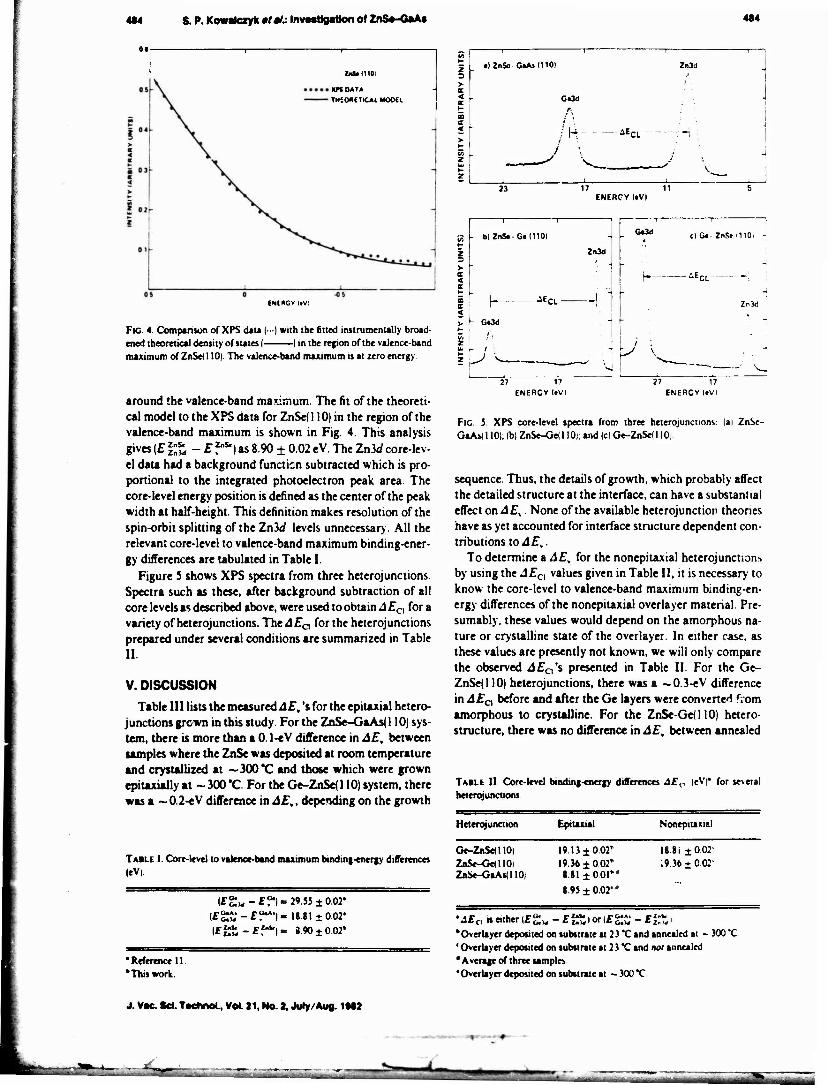
GaAs,11, GaAs-AlAs,6 ZnSe-GaAs7 and ZnSe-Ge7 heterojunctions.
Early in the program, it was found possible to measure changes in
band discontinuities (relative values) with very high precision (+ 0.01 eV)
simply by monitoring changes in core-level binding-energy differences between
atoms located on opposite sides of an abrupt heterojunction interface. This
excellent sensitivity led to the discovery that microscopic dipoles present at
abrupt heterojunction interfaces can substantially affect observed band dis-
continuities. Variations in heterojunction band discontinuities were observed
as functions of crystallographic orientation, »** growth sequence6,7 and
growth conditions. • It was also demonstrated by direct experimental test
that heterojunction band discontinuities are nontransitive; this result
established that band discontinuities depend on microscopic properties of the
interface and cannot be predicted from individual semiconductor properties
alone. The crystallographic orientation variation in band discontinuity for
Ge-GaAs heterojunctions was examined in some detail theoretically.-' From
electrostatic considerations, it was shown that polar interfaces cannot be
atomically abrupt, but require at least two interfacial transition planes to
be consistent with the experimental observations. The Fermi-level positions
and band discontinuities were determined for Ge-GaAs (110) heterojunctions as
a function of GaAs dopant type-, these studies found no evidence for the
presence of a dipole layer associated with interface defect levels.
3 C5570A/«*
• Rockwell International
MRDC41099.1FR
3.0 APPENDIX
This appendix reproduces publications supported by Contract No.
N00014-76-C-1109 in chronological order. These publications (which are
referenced in this final report) are:
1. "0bserv?.tion of the Orientation Dependence of Interface Dipole Energies in Ge-iaAs," R.W. Grant, J.R. Waldrop and E.A. Kraut, Phys. Rev. Lett. 40, 656 (1978).
2. "XPS Measurements of Abrupt Ge-GaAs Heterojunction Interfaces," R.W. Grant, J.R. Waldrop and E.A. Kraut, J. Vac. Sei. Technol. J_5, 1451 (1978).
3. "Polar Heterojunction Interfaces," W.A. Harrison, E.A. Kraut, J.R. Waldrop and R.W. Grant, Phys. Rev. B. _18, 4402 (1978).
4. "Semiconductor Heterojunction Interfaces: Nontransitivity of Energy-Band Discontinuities," J.R. Waldrop and R.W. Grant, Phys. Rev. Lett. 43, 1686 (1979).
5. "Precise Determination of the Valence-Band Edge in X-Ray Photoemission Spectra: Application to Measurement of Semiconductor Interface Poten- tials," E.A. Kraut, R.W. Grant, J.R. Waldrop and S.P. Kowalczyk, Phys. Rev. Lett. 44, 1520 (1980).
6. "XPS Measurement of GaAs-AlAs Heterojunction Band Discontinuities: Growth Sequence Dependence," J.R. Waldrop, S.P. Kowalczyk, R.W. Grant, E.A. Kraut and D.L. Miller, J. Vac. Sei. Technol. \9_, 573 (1981).
7. "Measurement of ZnSe-GaAs (110) and ZnSe-Ge (110) Heterojunction Band Discontinuities by X-Ray Photoelectron Spectroscopy (XPS)," S.P. Kowalczyk, E.A. Kraut, J.R. Waldrop and R.W. Grant, J. Vac. Sei. Technol. 2±t 482 (1982).
8. "Measurement of Potential at Semiconductor Interfaces by Electron Spec- troscopy," R.W. Grant, E.A. Kraut, S.P. Kowalczyk and J.R. Waldrop, J. Vac. Sei. Technol. B _l, 320 (1983).
9. "Band Discontinuities and Interface Fermi-Level Positions in Ge-GaAs (110) Heterojunctions," S.P. Kowalczyk, R.W. Grant, J.R. Waldrop and E.A. Kraut, J. Vac. Sei. Technol. B U 684 (1983).
4 C5570A/sn
*> Rockwell Irternational
MRDC41099.1FR
■'.
10. "Semiconductor Core-Level to Valence-Band Maximum Binding-Energy Differ- ences: Precise Determination by X-Ray Photoelectron Spectroscopy," E.A. Kraut, R.W. Grant, J.R. Waldrop and S.P.Kowalczyk, Phys. Rev. B ^8, 1965 (1983).
11. "Valence-Band Discontinuities for Abrupt (110), (100) and (111) Oriented Ge-GaAs Heterojunctions," J.R. Waldrop, E.A. Kraut, S.P. Kowalczyk and R.W. Grant, Surf. Sei. 132, 513 (1983).
C5570A/sn
VOLUME 40, NLMBE* 10 PHYSICAL REVIEW LETTERS 6 MARCH 1<T8
Observation of the Orientation Dependence of Interface Dipole Energies in Ge-GaAs
R. W. Grant, J. R. Waldrop, and E. A. Kraut Selene« Center, Rockwell International, Thousand Oaks, California 91360
(Received 19 December 1977)
The Interfaces between a thin (*• 20-A) abrupt epitaxial layer of Ge grown on substrates of (111), (110), and (100) GaAs have been Investigated with x-ray photoelectron spectos- copy. Observed changes in core-level binding energies have been directly related to the crystallographs orientation dependence of interface dipoles and variations of band-gap discontinuities. The orientation variation of the band-gap discontinuities is found to be a significant fraction (fe \) of the total band-gap discontinuity.
There has been considerable theoretical inter- est in the properties of ideal abrupt interfaces between different semiconductors, stimulated in part by the recent progress in molecular beam epitaxy (MBE) whereby trvüy abrupt interfaces can now be achieved. A basic property of the abrupt semiconductor interface is the relative alignment of the energy bands of the two semicon- ductors; i.e., how the energy difference in the band gaps (AE,) is distributed between the va- lence- and conduction-band discontinuities (AE, and AE e) such that AE,« AE „ ♦ AE e.
The first and most widely used model for esti- mating AE c (or AE „) is based on electron affinity differences.1 Critical evaluations'*' have been made of this model. Alternative models for pre- dicting AE. have appeared,** and two self-consis- tent calculations of the Ge/GaAs-interface eUv tronic structure have been completed.1'1 Although It has long been recognized that interface dipoles could produce energy-b?nd discontinuities which depend on crystallographic orientation of the in- terface plane, such effects have generally been ignored. Transport measurements' on vapor- grown Ge/GaAs heterojunctions suggested that
there could be substantial (a few tenths of an eV) changes in valence- and conduction-band disconti- nuities, 6(A£V) and 6(AEC), dependent on crystal- lographic orientation. Unfortunately, it is rela- tively difficult to determine these dopant-level- independent quantities from transport measure- ments and the scatter in these data is as large as the measured effect.
To investigate the interface dipole orientation dependence, we have developed a contactless x- ray photoemission spectroscopy (XPS) technique which allows a direct probe of interface potential variations. Herein, we report the observation of sizable and systematic variations in A£v for the Ge/GaAs interface as a function of crystallograph- ic orientation. Figure 1 is a schematic energy- band diagram of an ideal abrupt Ge/GaAs inter- face. The relative positions of the average bulk crystal potential within the two semiconductors determine AE, and AE ,.**"* An orientationally dependent change in the interface dipole magni- tude may shift the relative positions of the va- lence and conduction bands in the two semicon- ductors as shown schematically by dashed lines in Fig. 1. Figure 1 also shows the position of a
VOLUME 40, NUMBER 10 PHYSICAL REVIEW LETTERS 6 MARCH 1978
Sä*i it
Htt i
v0
? «61.
?
FIG. 1. Schematic energy-band diagram. The dashed lines Illustrate a decreased value of A£u associated with an Interface dlpole layer that accelerates photo- electrons from a GaAs substrate relative to Ge id pho- toelectrons which do not cross the Interface.
core level in Ge and in GaAs. As the average bulk crystal potential changes to adjust to the di- pole variation, the relative binding energies of all levels on both sides of an abrupt interface (measured relative to the common Fermi level, £ r) must also vary by the change in dipole ener- gy with orientation; i.e., |6(^£v)| s|o(A.£e)| *|6(A£*)I also indicated by dased lines in Fig. 1. For the Ge/GaAs interface, we will specifically consider the energy separation, AE,, between the Ga 3d and Ge 3d core electron levels. A mea- surement of 6(oi£a) by XPS thus provides a direct measure of ö(A£,). The dashed lines in Fig. 1 illustrate a change in the interface dipole which would Increase the splitting between the Ga 3d and Ge 3d core levels to equal the decrease in AE..
Our experiment used Al Ka {ftv ■ 1486.6 eV) ra- diation in conjunction with an extensively modified Hewlett-Packard model 59S0A ESCA (electron spectroscopy for chemical analysis) spectrome- ter to excite photoelectrons from C-VGaAs inter- faces for which the Ge was an *20-A-thick layer on a thick (=0.5 mm) GaAs substrate. The es- cape depth for the Ge 3d and Ga 3d photoelectrons is «20 A. Thus, photoelectrons from both sides of the Ge/GaAs interface are observed simulta-
neously in the same XPS spectrum. Electrons which originate on the GaAs side of an abrupt in- terface pass through any dipole layer at the inter- face in order to be emitted from the free surface and detected, while electrons originating in the Ge do not. For example, an electron passing through a dipole layer in a direction from higher to lower electron density will experience an acce- leration and, consequently, a relative increase in hinetic energy proportional to the dipole mo- ment per unit area, T, at the interface.9 A kinet- ic-energy increase will appear as an apparent binding-energy decrease in the XPS spectrum. In terms of the average charge density p(z) over planes parallel to the interface, the dipole mo- ment per unit area is
T = /*p(*)d*.
The self-consistent calculations of Baraff, Appel- baum, and Hamann6 and Pickett, Louie, and Co- hen7 have shown that the potential variations near an interface are localized to within 1 or 2 atomic layers, a length considerably less than the Ge 3d and Ga 3d photoelectron escape depths.
Interface states and bulk doping differences which cause band bending can complicate the abil- ity to determine A£v from transport measure- ments. In the XPS techniques described here, however, because the photoelectron escape depth is much smaller than typical band-bending lengths £ (£ >103 A for moderate dopant \P S), the ef- fect of interface states is to shift .ie potential within the sampled region on both sides of an in- terface by 'he same constant value. Therefore, since AEa is the difference in core-level binding energy for photoelectrons which originate from each side of the interface, any potential shift due to interface states or other sources of band bend- ing cancel. It is assumed that the two semicon- ductors are nondegenerately doped and that the dimensions perpendicular to the Interface sam- pled by XPS are small compared to £.
The «rery thin (- 20-A) epitaxial layers of Ge used for these interface studies were grown with- in the XPS apparatus on heated (*425CC) GaAs substrates by evaporative MBE techniques simi- lar to those previously described,10 but at low flux rates. GaAs substrates with (100), (111), (TIT), and (110) faces were cut from a single boule of undoped GaAs (n-type carrier concentra- tion 10* cm')." Laue back-reflection photogra- phy showed that the substrates were oriented to better than 1°. Each substrate was etched in 3:1:1 HJSCVH.O^HJO prior to insertion into the
XPS vacuum system. Substrate surfaces were cleaned by ArMon sputtering (750 eV) followed by annealing at = 575CC to remove sputter damage (vacuum-system base pressure was low 10"10
Torr). Room-temperature low-energy electron- diffraction (LEED) patterns characteristic of (110) (lxl), (HDGa(2x2), (TTT)As(lxl), and (100)Ga c(8x2) were obtained. In addition, a (100)As surface was also studied which was ei- ther c(2xB) or (2x4). Additional LEED measure- ments confirmed the epitaxy of the Ge overlay era. Following the XPS measurements, a metal point contact was made to the semiconductor surface to ensure reasonable diode characteristics.
Figure 2 shows an XPS spectrum from a sam- ple of epitaxial Ge grown on a (110) (lxl) GaAt substrate. To determine &EB, a background function which is proportional to the integrated photoelectron area was subtracted from tht data to correct for the effect of inelastic photoelectron scattering. A£jwas measured between the cen- ters of the peak widths at half of the peak heights. This procedure made it unnecessary to resolve the spin-orbit splitting of the Ge 3d and Ga 3d lev«
n M IMMNCMIC« «VI
FIG. 2. XPS • pert rum tn the energy region of the O* id and Ge 3rf core level* obtained from a (110) Ge/GaAe Interface. The thickness of the epitaxial Ge overlayer waa • SO A.
els (=0.5 eV) to obtain high-precision peak posi- tions.
Measurement results of eight different inter- faces are given in Table I. In general, several (three to five) independent determinations were made on each interface. In all cases, measure- ment reproducibility was <0.01 eV and was usual- ly <0.005 eV; calibration uncertainties increase the error limits to 0.1 eV. The measurements on the two samples of (110) (lxl) and (TTT)As (lxl) reproduce very well. We believe u.r> dis- crepancy in the two values shown for (lll)Ga (2x2) is real and represents a subtle difference in the interface properties grown on this surface.
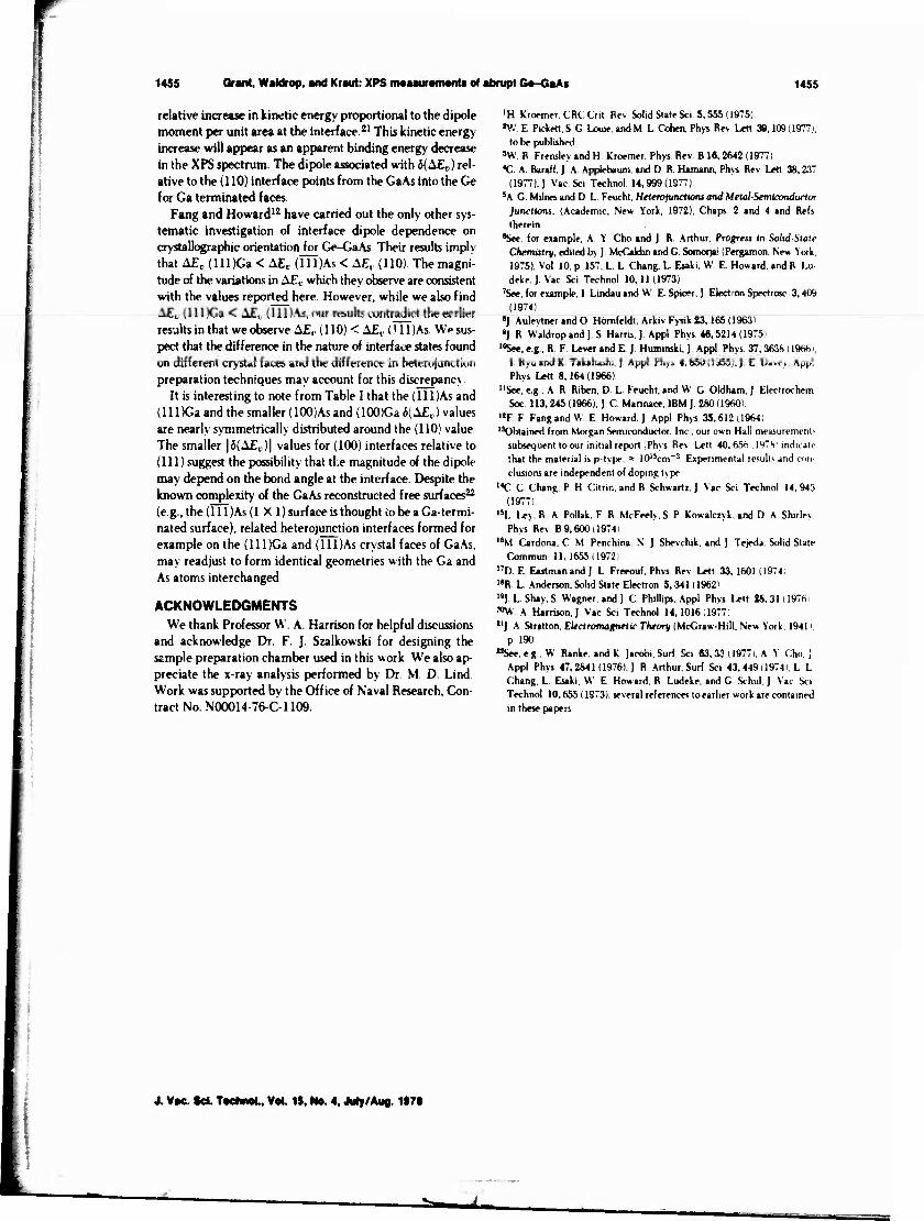
If we arbitrarily reference all 6(&E„) values to the (U0) charge-neutral surface such that o(A£„)nos0, we obtain the values of 6(A£„) shown in Table I. It is interesting that the (TTI)As and (lll)Ga and the (100)As and (100)Ga differences are nearly symmetrically distributed around the (110) value. However, the known complexity of these surfaces" makes a simple interpretation of the variations in valence-band discontinuity difficult.
In summary, a technique has been developed to observe directly variations in band-gap discon- tinuities at abrupt semiconductor interfaces, and systematic changes in &£t as a function of inter- face crystallographic orientation have been ob- served for Ge/GaAs. The maximum variation in AE,. between the (111) and (TTI) interfaces is *0.2 eV, which is a significant fraction (*«) of &E, (0.75 eV). This result suggests that accurate future models used to predict AE„ and AEC need to account for dipole orientation dependence.
We acknowledge helpful discussions with Profes-
TABLE I. Ge-3rf-Ga-3rf binding- energy- differences and corresponding variations In valence-band discon- tinuity for various Ge/GaAs interfaces.
Substrate surface
A£4 (cV)
6(A£.) (eV)
mir-. 10.27 ±0.01 *-0.085 ii*ii 10.3W0.01
(100)Ga ev8*2) 10.22*0.01 -0.015
(110) 10.20*0.01 0 (lxl) 10.21*0.01
(100)Aa 10.17*0.01 «0.035
(TTHAa 10.11*0.01 «0.10 (1*1) 10.10*0.01
651
-=Z_ .-/
F
VOLUME 40, NtMsri 10 PHYSICAL REV1EVC LETTERS 6 MARCH 1978
sor W. A. Harrison and appreciate the x-ray anal- ysis performed by Dr. M. D. Lind. This work was supported by the U. S. Office of Naval Re- search, Contract No. N00014-76-C-1109.
'R. L. Anderson. Solid-State Electronic. 5, 341 (1962). 2H. Kroeir.er. CRC Crlt. Rev. Solid State Scl. 5, 555
(1975). 5J. L. Shay, S. Wagner, and J. C. Phillips, Appl.
Phys. Lett. 2H. 31 (1976). 4W. A- Harrison, J. Vac. Sei. Technol. U, 1016
(1977). *W. R. Frensley and H. Kroemer, Phys. Rev. 16,
2642(1977).
iC. A. Baraff, J. A. Appelbaum, and D. R. Hamann, Phys. Rev. Lett. 38, 237 (1977), and J. Vac. Sei. Tech- nol. 14, 999 (1977).
'W. E. Pickett, S. G. Louie, and M. L. Cohen, Phys. Rev. Lett. 39, 109 (1977), and to be published.
'F. F. Fang and W. E. Howard. J. Appl. Phys. 35, 612 (1964).
*J. A. Stratton, Flectrotnagnetic Theory (McGraw- Hill. New York. 1941), p. 190.
WR. F. Lever and E. J. Humtnski, J. Appl. Phys. 37, 3638(1966).
"Obtained from Morgan Semiconductor, Inc. "See, e.g.. W. Ranke and K. Jacobi, Surf. Set. 63, 33
(1977); A. Y. Cho. J. Appl. Phys. 47, 2841 (1976); J. R. Arthur, Surf. Sei. 43, 449 (1974); L. L. Chang. L Esa- ki, W. E. Howard, R. Ludeke, and G. Schul, J. Vsc. Sei. Technol. 1J), 655 (1973); several references to earlier work are contained in these papers.
659
._/
XPS measurements of abrupt Ge-GaAs heterojunction interfaces
R. W. Grant, J. R. WaWrop, and E. A. Kraut
Rockwell International Science Ctnttr, Thousand Oaks. California 91360
(Received 24 January 1978; accepted 17 April 1978)
A method has been developed to grow thin epitaxial layers of Ge on GaAs substrates within an XPS system by an evaporative MBE technique. Abrupt heterojunctions with Ge layer thicknesses of =20 A have been grown on (111), (110), and (100) GaAs crystal faces. By using XPS data obtained oi these heterojunctions, variations in band gap discontinuities related to the crystallographic orientation dependence of interface dipoles have been observed directly. The data are also used to make an initial estimate of the valence band discontinuity for the abrupt Ge-GaAs heterojunction and with refinement of the technique, accurate values for this quantity should be obtainable.
PACS numbers: 73.40.Lq, 79.60.-i
I. INTRODUCTION
The use of heterojunctions in semiconductor devices can provide selective control over carrier transport properties which is unobtainable with single semiconductor devices This effect arises from the energy band discontinuities which occur at a heterojunction; the total energy band gap discontinuity is A£( and is equal to the difference in energy band gaps of the semiconductor pair The distribution of AEg between the valence and conduction bands, A£t, and A£f, respectively, has fundamental interest as well as importance to semicon- ductor device design and understanding of device charac- teristics (clearly, A£, " A£„ + AEC). The relative positions of the average bulk crystal potential determines A£t and AEC. l_4 An orientationally dependent change in the interface dipole magnitude may shift the relative positions of the va- lence and conduction bands in the two semiconductors If variations in band edge discontinuities are sizable, eg , with respect to the thermal energy, they may also be important considerations for carrier transport within semiconductor devices.
Previous experimental investigations of heterojunction band discontinuities and the dependence of these discontinuities on crystallographic orientation have involved analysis of transport measurements to extract the information.5 Unfor- tunately, it is relatively difficult to determine with precision these dopant level independent -n^ntities from transport measurements and the scatter in reported results is frequently large. In this paper, we will describe a new technique which employs x-ray photoelectron spectroscopy (XPS) in con- junction with abrupt heterojunctions grown by molecular- beam epitaxy (MBE) to study heterojunction band discon- tinuities. The method is a contactless potential probe of the junction which does not involve transport measurements We have investigated abrupt Ge/GaAs interfaces with particular emphasis on thi* variation of A£r with crystallographic ori- entation.
II. EXPERIMENT RATIONALE
The recent progress6 in MBE whereby truly abrupt het-
erojunctions can now be fabricated has at least in part stim- ulated considerable theoretical interest in the properties of ideal abrupt interfaces. Two self-consistent calculations of the Ge-GaAs interface electronic structure have been com- pleted.2-4 Both of these calculations have shown that potential variations near the abrupt junction are localized to within 1 or 2 atomic layers normal to the interface
The escape depth for energetic electrons excited within a solid by some form of incident radiation increases monoton- ically from *5 to *25 A as the electron kinetic energy in- creases from about 100 to 1500 eV.7 Thus, the unscattered photoelectrons observed in a particular XPS peak which have kinetic energies £1000 eV sample over a distance which is Urge compared to the distance over which potential variations occur near an abrupt interface. If one can prepare a large area abrupt heterojunction sample which consists of a very thin top layer of one semiconductor (»20 Ä thickness) grown onto a different semiconductor, it is possible to observe directlv photoelectrons which originate from both sides of the junction in the same XPS spectrum As we describe below, such an experimental arrangement can be used to study directlv the band discontinuities at an abrupt heterojunction A large photoelectron escape depth of several atomic layers will avoid unnecessary complications caused by any potential variation spread over 1 or 2 atomic layers at the abrupt interface However, from another viewpoint, complications due to band bending in the two semiconductors must be considered Typical band bending lengths for moderately doped semi- conductors are 500-1000 A. The potential variation due to band bending in the interface region sampled by XPS should be small relative to the accuracy with which one is attempting to measure the band discontinuities Thus, a sampling depth of *20 A seems mos» suitable for the experiment described here
Most XPS studies of core levels capitalize on variations in binding energies caused by chemical bonding effects which affect inner shell screening However, it has long been rec- ognized8 that the potential variations produced by changes in the Fermi level position in the surface region of semicon- ductor and insulator samples can also be observed as binding
MSI J. Vac. Sei TadMoL 1S(4), JUL/AHO, ItTS 002X-UU/7S/1S04-14S1S01.00 « 1«7i American Vacuum Society 1451
1452 Grant, Waldrop, and Kraut: XPS meaauramanta or abrupt Ga-GaAs 1452
GeW
Fir. 1 Schematic energy band diagram for an abrupt Ge-GaAs hetero- junction The dimensions perpendicular tc the interface are assumed to be small compared to the band bending length and thus band bending is ne- glected Various quantities indicated in the figure are defined in the teit.
energy variations in XPS spectra. We will use the latter effect, namely, the use of XPS as a potential probe, to study hetero- junction discontinuities. Auger electron spectroscopy has previously been used for potential probing a semiconductor p-n junction.9
To illustrate the use of XPS for studying heterojunction band discontinuities, we show in Fig. 1 a schematic band di- agram of an ideal abrupt heterojunction, Although an abrupt Ge/GaAs heterojunction is illustrated, as this is the interface reported on here, the technique is completely general for any abrupt heterojunction. With appropriate change of algebraic signs the expression given below for AE„ at Ge-GaAs is easily generalized to other heterojunction pairs. For samples with electrical contact between sample and spectrometer, the XPS binding energies Eg are usually referenced to a common Fermi energy, Ep. Although we will use this concept in the following discussion (i.e.. Eg * 0 at Ei-), the choice of a ref- erence energy can be arbitrary. A potential variation caused by the presence of an abrupt interface, or free surface or in- terface states, causes the energy positions of all bands, in- cluding the very narrow core level bands, to shift in energy. Within «ach individual semiconductor all bands will shift by an equal energy. If the barA bending lengths are considerably greater than the XPS sampling depth (as we have assumed in Fig. 1), then the presence of surface or interface states will shift all energy levels measured by XPS in both semiconduc- tors which form an abrupt heterojunction by the same amount By referring to Fig 1, a very simple expression is obtained for A£t,, namely
AEt,-(E£'M-E^)-(Ea-M-E^A')-AEB (1)
where Eg*M and Ej* are the binding energies of the Ge 3d core level and valence-band edge, respectively, in bulk Ge; Eg*u and ££*** are the binding energies of the Ga 3d core level and valence-band edge, respectively, in bulk GaAs. AEB
J. Vac. Set. TachnoL, Vo!. IS, No. 4. Jury/Aug. 1«7»
is the energy difference between the Ge 3d and Ga 3d levels measured with a Ge-GaAs heterojunction sample. Thus, we see from Eq. (1) that if the bulk core level binding energy relative to the valence band edge is known for both semi- conductors which form a heterojunction, an XPS measure- ment of AEB at an abrupt interface with the sample geometry described above will provide a direct measure of A£„.
At least two approaches might be tried to obtain the re- quired very thin MBE-grown epitaxial layers. One might grow a layer somewhat thicker than necessary in a dedicated MBE apparatus, transfer the sample to the XPS apparatus and use a combination of sputtering and annealing (to remove sputter damage) to reduce the epitaxial layer to the desired thickness. Alternatively, the very thin epitaxial layer could be grown in place within the ultrahigh vacuum XPS system, as we chose to do. This latter approach avoids any use of sputtering to remove surface contamination or thin the epi- taxial overlayer.
The semiconductor pair Ge/GaAs was chosen for study because of the nearly perfect lattice matching of this pair In addition, by growing Ge on GaAs substrates, a very simple "single-cell" MBE system could be us<<l. Considerable ex- perience with both evaporative10 and vapor growth11 of Ge on GaAs has been reported. The Ge/GaAs heterojunction has interesting device applications and as we will discuss in some detail below, it is the one system where a strong systematic variation in AE„ (or A£c) with crystallographic orientation has been reported.12
III. EXPERIMENTAL
A schematic diagram of the experimental apparatus is shown in Fig 2. A HP 5950A ESCA spectrometer with a completely redesigned sample preparation chamber was used. This spectrometer employed monochromatic AlK0 radiation (hv — 1486.6 eV) as the source of photoelectric excitation. A long high-vacuum bellows is used in conjunction with the movable sample rod. The base pressure in the bakeable sample preparation chamber was in the low 1CT10 Torr range. The essential instrumentation on the sample preparation chamber included a LEED system, a rastered ion sputter gun, a Ge evaporation system with a shutter to interrupt the beam, and a quartz crystal film thickness deposition monitor. The sample holder incorporates a heater and thermocouple arrangement
2 trl •ASTtICO
IM
on
n
SCHEMATIC DIAGRAM Of EXPERIMENTAL APPARATUS
KK; 2. Sehr latkr diagram illustrating eaential components of experimental apparatus-
of abrupt Ga-GaAa 1453
M 24
BINDING ENERGY ItVl
FlC. 3. Representative XPS spectrum in the region of the Ci 3d and Ge 3d core levels obtained from a (110) Ce-CaAs interface.
Room-temperature LEED patterns of the GaAs substrates characteristic of (110) (1 X 1), (lll)Ga (2 X 2), (Ul)As (1 X 1) and (100)Ca c(8 X 2) were obtained. In addition, a (100)As surface was also studied which was either c(2 X 8) or (2X4) Following the XPS measurement, a metal point-contact v as made to the semiconductor surface to ensure reasonable diode characteristics.
IV. RESULTS
A. Measurement of AE»
In Fig. 3, we show an XPS spectrum obtained from a sample consisting of a thin epitaxial layer of Ge grown on a GaAs (110) (1 X 1) substrate. A background function which is proportional to the integrated photoelectron peak area was subtracted from the data to correct for the effect of inelastic photoelectron scattering. The quantity A£B is measured be- tween the centers of the peak widths at half of the peak heights. This procedure made it unnecessary to resolve the spin-orbit splitting of the Ge 3d and Ga 3d levels («0.5 eV) to obtain high precision peak positions.
In all, 33 independent measurements were made on eight different heterojunctions. In Fig. 4 we show representative background subtracted XPS spectra obtained from samples having each of the crystallographic faces studied. Each peak has been normalized to an equal height for easy comparison
A temperature controller is used to hold the sample temper- ature between room temperature and *1000°C. The GaAs substrate material was attached to a Mo metal holder with In
All the GaAs substrates were cut from a single boule of GaAs.13 Substrate crystal faces with (111), (ITT), (100), and (110) orientations were investigated. The orientation of the substrate materials was confirmed with Laue back-reflection x-ray photography and found to be better than 1 °. Following chemical lapping, each substrate was etched in 3:1:1 H2SO4: HJGYHJO prior to insertion into the XPS vacuum system.
After insertion into the sample preparation chamber, GaAs substrates were cleaned by sputtering with 750-eV Ar4 ions. The GaAs was held at 575° C during sputtering and was sub- sequently annealed at this temperature for «10 min to remove sputter damage. Ti sublimation pumping was employed during sputtering to minimize any reactive background gases. After annealing, the surface cleanliness was assessed by XPS and the removal of sputter damage was confirmed by LEED.
The Ge evaporation source consisted of a simple resistively heated W wire-wound basket filled with undoped n-type (* 1014 cm"3) Ge. After stablizing the evaporation rate to ~i A/s as measured by the quartz deposition monitor, a *20-A layer of Ge was grown on the GaAs substrate. The Ge source to substrate distance was «12 in. and a mechanical shutter was used to initiate and terminate growth. During Ge growth the GaAs substrate was held at 425°C. After growth the sample was cooled to room temperature and LEED was used to confirm the epitaxy of the Ge overlayer.
> «un« 10 oiaoii a u ■ •>
FKi XPS spectra in the region of the Ga3d and Ge 3d coreleveb obtained for five different Ce-CaAi interface» The GaAl substrate faces on which the thin epitaxial Ge overlayer» were grown ate indicated in the figure The vertical hue* indicate the ccntratds of the vano-is peaks as discussed in the text
J. Vac ScL TaetaieL, Vet 18, Mo. 4, Juty/Aug. 1171
1454 Grant, Waldrop, and Kraul: XPS meaauramonta of abrupt Qa-GaA* 1454
TABLE l Ge 3d - Ga id binding energy differences, linewidths, Ge epitaxial layer thicknesses and variation in valence-band discontinuities for various Ge-GaAs interfaces
(TTT)As 10 II ±01 1 21 ± 01 1 32 ± 01 13 +0 10 11X11 (llllAs 10.10 ± .01 1.22 ±.01 I28±.0i 18 +0 10 (1 x II
in the figure and the centroid (which we define as the center of the peak width at half peak height) of each peak is indi- cated by a vertical solid line in the figure. The centroids of the five Ga 3d peaks have been aligned in the figure. The dashed vertical reference line which runs through the Ge 3d peaks is the centroid of the Ge 3d peak observed from the hetero- junction which was grown on the GaAs (11 DGa (2 X 2) sub- strate. In Fig. 4 it is clearly observed that AEg is dependent on the crystallographic orientation of the interface; we will return to a discussion of this observation below.
Measurement results on the eight different interfaces are given in Table I. In general, three to five independent mea- surements were made on each interface and the averaged values are presented in the table. In all cases, measurement reproducibility for AEg was < ±0.01 eV and in most cases it was < ±0.005 eV. Calibration uncertainties increase the total error limits for AEg to ±0.01 eV In the table, we also list values for the average linewidths T of the Ge 3d and Ga 3d levels which were measured at half of the peak height. If a sizable potential variation occurred either within the het- erojunction area sampled by XPS or within the photoelectron escape depth, one would expect this variation to affect I\ Although the values of T scatter somewhat there is little sig- nificant systematic variation with crystallographic orientation (the r's observed on the (lll)As faces seem to be slightly larger than on the other faces). We also list the Ge epitaxial layer thicknesses in the Table. This thickness was calculated from the relative Ge 3d to Ga 3d line intensities by assuming an escape depth of 20 A and equal photoelectric cross sections for the two lines.
B. AEr Considerations By using the A£g values given in Table I, in conjunction
with Eq. (1), we could now calculate AE„ if accurate values of (£?" - E?) and (E^u - Ej4*") were known. Several determinations of (Ej*M - E?4*") have been reported for bulk
J. Vac. Set. Tachnol., Vol. 15. No. 4, My/Aug. 1»7t
GaAs; these are 18.9 ± 0.1 eV,u 18.82 ± 0.15eV,15 189 ± 0.1 eV,16 and 18.8 ± 0 1 eV.17 Our own estimate is 19 0 eV For (Ef M - E?) in bulk Ge, values of 29.0 ± 0.1 eV1* and 29.3 ±0.1 eV17 are reported; our own estimate is 29.5 eV. At present, the uncertainty of our own estimates is * ±0.2 eV. By using values from Refs 16 and 17, we obtain A£„ = — 0.10 ± 0.14 eV and AE„ = +0.30 ± 0.14 eV, respectively; our own estimates give AEC = +0.3 ± 0.3 eV for the (110) Ge-GaAs interface. Clearly, it will be necessary to obtain more accurate values of (E§* M - £<*) and (E^" - E?,As) before mean- ingful comparisons with theory can be made; we expect to report refined values in a later publication.
C. Measurement of S( AEv)
The main difficulty in determining accurate values for {Efr*4 -E?) and (E§'M - E^) in bulk Ge and GaAs, respectively, lies with the accuracy to which E^* or E^**1 can be determined from the XPS data.
However the change in A£„ with crystallographic orien- tation, which we will define as 5(AE„), can be determined to the same accuracy as which the Ge 3d and Ga 3d line centroid positions are determined If we set (Efid - E^) - (E£"M
— E^tAi) = C, where C is a materials constant, then Eq. (1) becomes AE„ = C — AEg- If we now denote the values of A£t
observed on tv/o different crystallographically oriented in- terfaces by subscripts 1 and 2, 6(A£V.) becomes
6(A£J = (AE„), - (AE„)2 = (A£„)2 - (AEB) (2)
and the poorly known value of C is eliminated. In Table I, we tabulate values of rj(A£t,) which have arbitrarily been ref- erenced to the (110) charge neutral surface such that rS(AE,,)no - 0; the values of AEg used to calculate 6(A£,,) are also given in Table I.
The measurements on the two samples of (110) (1 X 1) and (Ul)As(l X 1) reproduce very well The discrepancy in the two values shown for (11 DGa (2 X 2) seems to be real and most likely represents a subtle difference in the properties of these two interfaces.
V. DISCUSSION
The first and most widely used model for estimating AE, (or AEB) is based on electron affinity differences.'8 Critical evaluations11* have been made of this model and alternative models for predicting AE„ have appeared.1"410 Although it has been recognized that interface dipoles could produce energy band discontinuities which depend on crystallographic orientation of the interface plane, such effects have generally been ignored. The experiment described herein provides a sensitive method to probe variations in the interface dipoles as can be seen from Eq. (2).
Specifically, considering the interface formed by a thin Ge epitaxial overlayer grown on a GaAs substrate, photoelectTons which originate on the GaAs side of the abrupt interface must pass through any dipole layer at the interface before being emitted from the free surface to be detected, photoelectrons originating in .he Ge do not An electron which passes through the dipole layer in a direction from higher to lower electron density will experience an acceleration and consequently a
1455 Grant, Waldrop, and Kraut: XPS moaauramonta of abrupt Ga-GaAs 1455
relative increase in kinetic energy proportional to the dipole moment per unit area at the interface.21 This kinetic energy increase will appear as an apparent binding energy decrease in the XPS spectrum. The dipole associated with 6(AEJ rel- ative to the (110) interface points from the GaAs into the Ge for Ga terminated faces
Fang and Howard12 have carried out the only other sys- tematic investigation of interface dipole dependence on crystallographic orientation for Ge-GaAs Their results imply that A£„ (lll)Ga < A£t. (Ill)As < AEV (110). The magni- tude of the variations in A£t. which they observe are consistent with the values reported here. However, while we also find AE„ (lll)Ga < AE„ (lll)As, our results contradict the earlier results in that we observe A£c (110) < A£t, () 11 )As We sus- pect that the difference in the nature of interface states found on different crystal faces and the difference in heterojunction preparation techniques may account for this discrepancy.
It is interesting to note from Table I that the (111)As and (lll)Ga and the smaller (100)As and (100)Ca 6(AE„) values are nearly symmetrically distributed around the (110) value The smaller |d(A£^)| values for (100) interfaces relative to (111) suggest the possibility that the magnitude of the dipole may depend on the bond angle at the interface. Despite the known complexity of the GaAs reconstructed free surfaces22
(e.g.,the(lll)As(l X 1) surface is thought io be a Ga-termi- nated surface), related heterojunction interfaces formed for example on the (lll)Ga and (lll)As crystal faces of GaAs, may readjust to form identical geometries with the Ga and As atoms interchanged.
ACKNOWLEDGMENTS We thank Professor W. A. Harrison for helpful discussions
and acknowledge Dr. F. J. Szalkowski for designing the sample preparation chamber used in this work. We also ap- preciate the x-ray analysis performed by Dr. M. D. Lind. Work was supported by the Office of Naval Research, Con- tract No. N00014-76-C-1109.
'H Kroemer, CRC Crit Rev Solid State Sei 5,555 (1975) «W. E Pickett. S G Louie, and M L Cohen. Phys Rev Lett 39,109 (1977),
to be published 5W R Frensley and H Kroemer, Phys Rev B 18,2642 (1977) *G A Baraff. J A Applebaum, and D R Hamann, Phys Rev Lett 38,237
(1977); J Vac Sei Technol 14,999(1977) 5A G Milnes and D L Feucht, Heterofuncttons and Metal-Semiconductor
junctions, (Academic, New York, 1972), Chaps 2 and 4 and Refs therein
"See. for example, A Y Cho and J R. Arthur, Progress in Solid-Staff Chemistry, edited by ] McCaldin and C Somotja! (Pergamon. New York. 1975), Vol 10, p 157, L L Chang, L Esaki, W E Howard, and R Lu- deke, J Vac Sei Technol 10,11 (1973)
'See, for example, 1 Lindau and W. E Spicer, j Electron Spectrosc 3,409 (1974)
»J Auleytner and O Hörnfeldt, Arkiv Fysik 43,165 (1963) •J R Waldrop and J S Harris. J Appl Phys 46,5214 (1975)
10See, eg, R. F Lever and E. J Humiraki, J Appl Phys 37,3638 (19661, 1 Ryu and K Takahashi, J Appl Phys. 4.850 (1955), J E Dave\. Appl Phys Lett 8,164(1966)
"See, e.g., A. R Riben, D L Feucht, and W G Oldham, J Electrochem Soc 113,245 (1966), J C Mannace. IBM J 280 (1960)
"FF Fang and W E Howard.) Appl Phys 35.612(1964) 13Obtained from Morgan Semiconductor, lnc , our own Hall measurement'
subsequent to our initial report |Phys Rev Lett 40,65d \ 197S' indicate that the material is p-type. * 1015cm~3 Experimental results and con elusions are independent of doping type
'«C C Chang P H Citrin. and B Schwartz. J Vac Sei Technol 14,943 (19771.
15L Ley, R A Pollak F R McFeely, S P Kowalczyk. and D A Shirle>. Phys Rev B9,600(19741
'*M Cardona. C M Penchina N J Shevchik, and J Tejeda Solid State Commun 11.1655(1972!
nD E Eastman and J L Freeouf. Phys Rev Lett 33,1601 (19741 '•R. L Anderson, Solid State Electron 5,341 (1962> »*J L Shay, S Wagner, and ] C Phillips. Appl Phys Lett 88,31 (1976i *W. A Harrison, ] Vac Sei Technol 14,1016 (1977) "J A Stratton, Electromagnetic Theory (McGraw-Hill. New York. 1941).
p 190 •"See, eg W Ranke, and K Jacobi, Surf Sei «3,33 (19771. A Y Cho J
Appl Phys 47,2841 (1976), J R Arthur. Surf Sei 43.449(1974). L L Chang, L Esaki. W E Howard. R Ludeke. and G Schul.) Vac Sei Technol 10,655 (1873), several references to earlier work are contained in these papers
X Vac Sei. TaohnoL, Vol. IS, No. 4, My/Aug. 1*71
Jäa
PHYSICAL REVIEW B VOLUME IB, NUMBER 8 15 OCTOBER 1978
il
Polar heterojunction interfaces
W. A. Harrison,* E. A. Kraut, J. R. Waldrop, and R. W. Grant Sewn« Critter. Rockwell International. Thousand Oaks, California 91360
(Received 9 June 1978)
A study of heterojunction interface geometry based on our measured differences in 3d core-state binding energies for germanium and gallium at Ge-GaAs heterojunctions of different crystallographic orientations is reported. For the interfaces which have teen studied, i.e., (110), (100) Ga, (100) As, (111) Ga, and (Til) As, orientation-dependent variations in dipole contributions to valence-band discontinuities of about 0.2 eV have been observed. From electrostatic considerations we deduce the simplest interface geometries consistent with the facts that the differences are small and no large charge accumulations can occur at the junction. An abrupt planar junction is allowed for the (110) interface, but the polar interfaces require at least two transition planet, of atoms with compositions which are deduced from the two conditions above. The electrostatic calculations were based upon the differences in nuclear charge and are unaffected by the resulting polarization of the bonds if that polarization is described in an "electronegativity" approximation. In this approximation there would in fact be no dipole shift for the idea! geometries proposed. An improved treatment of the bond polarization based upon the bond-orbital model gives residual dipole shifts somewhat smaller than those observed, and in poor agreement with our measurements. Inclusion of lattice-distortion effects at the interface also fails to account for the observed dipole shifts. We conclude that the experimentally prepared junctions must contain deviations from the ideal atom arrangements The number of these deviations required to account for the observed shifts is on the order of one for every fifteen interface atoms.
I. INTRODUCTION
It has been possible to understand the essential properties of heterojunctions without concern for the possibility of electrostatic dipole shifts at the interface. Band-edge discontinuities could be predicted from differences in experimental elec- tron affinities' or theoretically from differences in bulk energy bands.2 A direct estimate of the dipole for a Si-Ge Junction,* a detailed treatment of the Ge-GaAs nonpolar (110) junction by Picket, Louie, and Cohen,' and general considerations of junctions by Frensley and Kroemer* all suggested that indeed the dipole effects should be small, at most on the scale of a few tenths of an eV.
If, however, there were no electrostatic dipole shifts at the interface, the band-edge discon- tinuities would necessarily be identical for any pair of materials, independent of the crystal orientation of the interface separating them. Thus a measure of differences for different crystal faces can give unambiguous evidence for dipole shifts and experimental distinction of dipole shifts from intrinsic band-energy differences associated with electron affinities. We analyze here a direct measurement of the differences in dipole shifts on different interfaces for Ge-GaAs heterojunc- tions,' and thus the first direct evidence of elec- trostatic dipole shifts.
To see what these measurements can tell us
about the junction, we need a formulation of the electrostatic properties of the different junctions. This leads immediately to the fact that properties such as dipole shifts are extremely sensitive to the detailed geometry of the interface. Because details are not known experimentally, we use the experimental findings, with the electrostatic formulation, to learn about the geometry. We find that the analysis places rather stringent conditions on the geometries which must exist in the experi- mental systems.
In Sec. II, the experimental results concerning the measurement of the relative dipole shifts are briefly summarized. In Sec. Ill, we make a care- ful formulation of the electrostatics for (110). (100), and (111) interfaces, and include bond di- pole s in a simple approximation, finding that the ideal planar geometry is not allowed for the polar interfaces. We then proceed to find the simplest geometry which is consistent with the experimen- tal findings of only small shifts. Geometries are in fact found which give no shift at all and the problem becomes that of understanding th > ob- served small shifts. Improvements in the calcu- lation of electron redistribution, discussed in Sec. IV, do not account tor them, nor do lattice distortions suggested by covalent radii, and dis- cussed in Sec. V. In Sec. VI, we conclude that the experimentally prepared junctions must contain deviations from the proposed ideal-atom arrange- ments.
II. SUMMARY OF EXPERIMENTAL RESULTS FOR Ge-GiAs HETEROJUNCTIONS
For convenience, in this section we briefly summarize our experimental findings on the rela- tive dipole shifts for Ge-GaAs heterojunctions with different crystallographic orientations. These results which employ x-ray photoeler^-on spectro- scopy (XPS) as the primary measurement tech- nique have now been reported.'
Substrates of GaAs with (100), (111), (111), and (110) faces were cleaned within the XPS vacuum system by Ar*-ion sputtering (750 eV) followed by annealing at about 575 °C to remove sputter damage. After annealing the surface, cleanliness was confirmed by XPS and the removal of sputter damage was assessed by low-energy electron dif- fraction (LEED). Very thin (»20 A) epitaxial layers of Ge were grown within the XPS appara- tus on heated (»425°C) GaAs substrates by evapor- ative molecular beam epitaxy (MBE) techniques. Additional LEED measurements confirmed the epitaxy of the Ge overlayers. XPS was used to measure the differences in Ge-3d and Ga-3d core- level binding energies at Ge-GaAs heterojunctions with different crystallographic orientations. As discussed in Ref. 5, observed changes in core- level binding energies provide a direct measure of the crystallographic orientation dependence of interface dipoles and variations of band-gap dis- continuities.
Measurements were carried out on eight dif- ferent interfaces. In Table I we summarize the results. Additional experimental details may be found in Ref. 5.
III. THEORY OF THE DIPOLE SHIFT
We are concerned here with potentials arising from infinite arrays of charges, a type of prob- lem known to be very tricky and even to lead to conditionally convergent answers in some cases. It is therefore absolutely essential to proceed with care and to be certain that we include the essential physical effects correctly. A model of the system may not be adequate; we must treat the system it- self.
To do this we start with a plane (to become the
TABLE I. Ge 3d-Ga 3d binding energy differences A£«for various Ge-GaAs heterojunctions. All error limits are »0.01 eV.
Substrate surface (111) Ga (100) Ga (110) (100) As (TU) As
junction plane) through a germanium crystal, with germanium atoms extending indefinitely on both sides. We Imagine having solved for the electronic states in this system which by definition has no dipole shift across the junction. We will then "freeze" the electronic structure and imagine transferring protons between nuclei to the right of the junction such as to convert half of the nuclei to gallium (atomic number one less than germa- nium) and half to arsenic (atomic number one greater than germanium). This shift of protons (theoretical alchemy6) will of course produce an exactly calculable change in electrostatic poten- tial and may produce an accumulation of nuclear charge at the interface or a dipole layer at the interface. [In fact, both occur at polar inter- faces, (100) and (111).] We then allow the elec- tronic system to relax, which if done sufficiently accurately would lead to a precise description of the true Ge-GaAs heterojunction with this parti- cular set of germanium, gallium, and arsenic atom positions. The change in electronic struc- ture can, of course, only be done approximately but the most important qualitative features can be obtained rigorously.
We begin with a discussion of the (110) inter- face, which provides a reference for the other interfaces. Shown in Fig. 1 is a Ge-GaAs (110) interface resulting from the transfer of protons,
8
o- Gt
• - Gl
o- As
[110]
AC, (eV) 10.27 10.31
10.20 10.11 10.22 10.17 10.21 10.10
FIG. 1. A (110) heterojunction between Ge and GaAs. The crystal is viewed along the iTlO] direction with the [0011 direction vertical. Note that every plane of atoms parallel to the junction is on the average neutral corres- ponding to a nonpolar junction. The symbols used to identify specific atoms are defined in this figure and are the same in all figures. All atoms are tetrahedrally bonded; the "double" bonds schematically illustrated in the figures are two tetrahedral bonds separated by the usual 109* tetrahedral bond angle and projected on to the plane of the figure.
-L.
4404 HARRISON, KRAUT, WALDROP, AND GRANT 18
with the electronic structure still frozen as in germanium. It is apparent from the figure that each plane of atoms parallel to the interface is still neutral on average. This corresponds to the transfer of protons parallel to the surface, per- haps downward in the figure. This also corre- sponds to no charge accumulation at the inter- face nor any electrostatic dipole layer. There are, of course, fluctuations in electrostatic po- tential along the interface, but the potential aver- aged over a plane parallel to the interface (which is equivalent to the potential at one point due to charges averaged over planes parallel to the sur- face) is unchanged. At a heterojunction interface, the terms dipole shift and charge accumulation are defined as a discontinuity in average potential and average potential slope, respectively. The average potential is defined as the potential aver- aged over a plane midway between adjacent atomic planes. We will return later to the relaxation of the electronic structure and see that its effect should be very small.
We turn next to a (100) interface shown in Fig. ?,. Again, think of the electronic structure as frozen to be the same as in germanium. In this case each plane of atoms parallel to the interface is charged; this corresponds to proton transfer perpendicular to the interface. The consequences of this transfer may not be immediately obvious, but we may again understand them by averaging the charge distribution over planes parallel to the interface. We may readily integrate Poisson's equation from the germanium on the left, where we take the potential to be constant and zero through the junction. The result is illustrated at the bot- tom of Fig. 2. Upon crossing the first plane of negatively charged atoms the potential gradient becomes positive and constant, and then becomes zero again after crossing the first plane of posi- tively charged atoms. Thus the potential in the GaAs contains an average gradient in addition to a fluctuating component; the average gradient may be thought of as coming from charge accumula- tion at the interface due to proton transfer, and therefore polarization density, perpendicular to the interface, and terminating at the interface. In any case, it is real and unambiguous and results in a potential which cannot be sustained in the real system because it leads to potential differences over a few atom distances which are greater than the band gap; spontaneous generation of car- riers would immediately occur.
Let us turn to the redistribution of the electrons due to the redistribution of protons. We look first at the response to the fluctuating component of the potential, with the average potential gradient subtracted. This becomes just the fluctuating po-
■[001] i
/ >
A
FIG. 2. A (001) heterojunction between Ge and GaAs, again viewed along the (TlO) direction with the [TTo] direction now vertical. Note that the first atomic plane to the right of the Junction ts entirely Ga lit is therefore called a (001) Ga junction] which, without bond polariza- tion, is negatively charged. The potential averaged over planes parallel to the junction, is obtained by Integrat- ing Poisson's equation from left to right. A nonzero average electric field has ar;^,. to the right of the junction due to charge accumulation. It is not elimin- ated by bond polarization although this will change the sign of the effective charge on the Ga (see Sec. IV).
tential which would arise in a bulk crystal from converting the germanium nuclei to gallium and arsenic nuclei |for example, by transferring pro- tons parallel to the surface of a slab with (110) surfaces]. The charge redistribution could be calculated rather reliably in a linear combination of atomic Orbitals (LCAO) context and in the bond- orbital model7 in particular, but the essential features are more easily understood in terms of an electronegativity approximation. In that ap- proximation we assert that the added proton lowers the energy of the atomic states on the arsenic atom, the removed proton raises the en- ergy on the gallium atom, and this effect polarizes the intervening bonds towards the arsenic. This will produce a dipole in the bond but no net change in the charge of two in the bond. Whatever charge is added to the arsenic is removed from the neigh- boring gallium atoms. This would follow from any nearest-neighbor (or higher-order neighbor) LCAO or Wannier-function calculation. It follows
18 POLAR HETEROJUNCTION INTERFACES 4405
that charge redistribution in the bonds at the in- terface cannot remove the charge accumula'ion which arose from the proton transfers.
We turn next to the average potential gradient, which has not been eliminated by the bond distor- tions. (In our construction this occurred in the GaAs, but it could as well have been in the Ge; it is the difference in gradients which is guaranteed by the electrostatic calculation.) This gradient will cause an additional polarization of each bond extending indefinitely to the right and therefore can cause a charge accumulation. This is just the dielectric polarization of GaAs and reduces the average field by a factor of the dielectric con- stant t. We are left with an average potential gradient which may be readily calculated. The charge density in each plane is 2e/a2, where a is the cube edge, 5.65 A for GaAs. The change in the potential gradient (Va# = -4np) is 4JT times this. To obtain the average gradient we divide by 2 and by the dielectric constant t = 10.9 for GaAs and multiply by e to obtain a change in electro- static potential energy of
6£=4ne2Aa = 2.9eV (1)
for each distance a. This corresponds to a huge field and, as we indicated earlier, would raise the valence band maximum at one point above the conduction-band minimum a few atom distances away, thus producing instantaneous carriers (in this case, one electron per area a2) and reducing the net charge at the interface to zero. This is exactly the result which Baraff, Appelbaum, and Hamann* obtained by detailed treatment of just this junction geometry. As Baraff' has empha- sized, it is guaranteed by this geometry of the junction.
There is, however, no experimental evidence for such a huge free-carrier density or such a large qualitative difference in junctions prepared upon (100) faces rather than (110) faces. Indeed, it is almost inconceivable that a junction could be prepared with one electron per surface atom in an antibonding (conduction-band) state. We there- fore postulate that the planar geometry must be modified to eliminate the excess charge; the planar geometry Shown in Fig. 2 is not expected to occur in a real junction. We proceed to seek the simplest modification which is acceptable.
The geometry of Fig. 2 produced fields which corresponded to a deficit of one proton for every two surface atoms at the junction. In terms of our theoretical alchemy one proton must be added for every two surface atoms. Note that this could be done by adding a proton to half of the gallium atoms in 'he first gallium plane to the right of the junction in Fig. 2, converting them to germanium
atoms, or it could be done by adding one to half of the last plane of germanium atoms to the left of the junction, converting them to arsenic atoms. There are innumerable other ways to add the pro- tons, but these two are the simplest; the first is illustrated in Fig. 3.
We may again average the charges over atom planes, leaving the electrons frozen in the ger- manium electronic structure, and integrate Poisson's equation through the junction as indi- cated below in Fig. 3. The added protons have eliminated the average potential gradient in the GaAs and therefore produce an allowed geometry in this regard. However, this geometry has pro- duced a shift in the average potential in the GaAs of 6 = nex/2a(. =0.37 eV. One way of seeing that there is a dipole shift here is to construct to the right of the GaAs shown in Fig. 3 the analogous junction with an extra half-plane of gallium atoms (so the entire system is neutral) aid with ger- manium to the right; that is, to construct a GaAs slab surrounded by germanium. We then see that the potential in the germanium to the right is shifted with respect to that on the left by twice the value given above. This large dipole did not occur on the (110) junction illustrated in Fig. 1 and is not consistent with the much smaller differences
[001] 1
6 1 A \ / i A \
I
FIG. 3. A (001) heterojunctlon as in Fig. 2, but with k of the Ga atoms in the junction plane replaced by Ge atoms. The average electric field in the GaAs has been eliminated but there is still a dipole shift o much larger than is experimentally observed. The dipole shift is not eliminated by bond polarization.
4406 HARRISON, KRAUT, WALDROP, AND GRANT 18
in dipole shifts on different surfaces which are ob- served (Sec. II). We conclude that this geometry also is not correct; however, the redistribution of electronic charge must first be considered.
We approximated the redistribution in terms of an increased electronegativity on each arsenic atom which polarized neighboring bonds in propor- tion to the electronegativity difference with the neighboring atoms. We may do this atom by atom near the junction and see immediately that the dipoles induced to the right of each atom are just equal and opposite to those on the left; no net di~ pole layer is introduced and the shift in average potential remains. Thus the geometry of Fig. 3 must be modified.
It is interesting that this same result was ob- tained by Frensley and Kroemer' who modeled the total charge distribution at a polar inteface by just such an electronegativity model. They found no charge accumulation and no dipole shifts for geometries such as those of Figs. 2 and 3. We note that this model omits the very important dif- ference in nuclear charges which is an essential feature of real junctions.
The conclusion of no net dipole layer would be modified slightly by a more realistic LCA:/ cal- culation. We will see in Sec. V that in the bond- orbital approximation,1 the excess electronic charge on the arsenic is not extracted equally from the neighbors on the two sides. This does not modify our earlier conclusion concerning total- charge accumulations, but it does introduce di- pole shifts of the order of a few hundreths of an eV for the geometries we have discussed. These are not large enough to cancel the 0.37 eV shift found above; thus we conclude that the (100) geometry, consisting of a single transition layer (the half-gallium layer of Fig. 3) does not occur.
The simplest modification which eliminates the dipole shift requires two transition layers, a I -gallium layer and a j -arsenic layer as sche- matically illustrated in Fig. 4. It seems appro- priate to think of this as a modification of a geometry with the last GaAs layer being gallium and we therefore refer to this as a (100) \ -Ga surface. The integration of Poisson's equation, shown below, indicates that there is no dipole shift nor charge accumulation. The second alter- native is a \ -arsenic and \ -gallium layer; it can be constructed by interchanging gallium and arsenic atoms in Fig. 4. We refer to it as the (100) \ -As junction. Either type of junction can be grown on a given (100) surface of GaAs, which we will see is in contrast to the (111) surface. All other allowed alternatives involve more than two transition planes and will not be considered. It would be difficult to {mess the precise pattern
-►[001)
FIG. 4. A (001) heterojunction as in Figs. 2 and 3, but with two transition planes. The first is \ As, the second \ Ga with the remaining atoms Ge; it is appro- priate to refer to It as a (100) j-Ga Junction. This is the simplest junction geometry which eliminates both charge accumulation and dipole shift.
which occurs in a real junction although elect '- static energies are usually lowered by high-s>.n- metry patterns. The geometries shown in Figs. 3-6 are only intended to illustrate the average composition of atom planes without specifying a two-dimensional symmetry pattern. The highest symmetry allowed for the (100) interface would be 1x4, but it is possible that a 2x4 pattern would have lower electrostatic energy.
It is fair to ask how such a pattern would arise experimentally. If it were possible to construct a planar junction, as in Fig. 2, with its sheet of compensating carriers, the chemical force deriv- able from the excess energy of electrons in anti- bonding states would cause diffusion of gallium atoms out of the junction or arsenic atoms in until there was no excess nuclear charge at the junction and no free carriers. In fact, a residual dipole would favor diffusion in such a way as to eliminate the dipole. It seems more likely, however, that the growth process itself produces a ncnplanar junction such as that shown in Fig. 4 directly, as an interface of lowest energy.
We have applied this same analysis to the (111) junctions, requiring that in the electronegativity
18 POLAR HETEROJUNCTION INTERFACES 4407
-♦[111] -►[111]
FIG. 5. A (111) heterojunction, viewed along the [OlT] direction, constructed on the (111) Ga face of GaAs. It is a two-transition-plane junction with the first plane 5 As and the second plane \ Ga. We call it a (lll)j-Ga junction. This is one of the two-plane geom- etries giving no charge accumulation nor dtpole shift, as seen in the potential plot below. The other is shown in Fig. 6.
approximation there be no charge accumulation nor dipole shift at the Junctions. In Fig. 5 we show a (111) interface. Note that along the [111 ] direction atomic planes are alternately connected by bonds parallel to the [111) direction and bonds (three times as many) inclined to that direction. Thus there are two distinct [111] directions and two crystallographically distinct (111) junctions; Fig. 5 illustrates the orientation with gallium atoms at the end of the parallel bonds away from the germanium. This is usually called the (111) Ga face since it is assumed that the crystal will terminate with the minimum number of bonds broken leading in this case to a Ga terminating plane. We find that for this crystallographic ar- rangement there are two kinds of interfaces with two transition planes which give no charge ac- cumulation and no dipole shift in the electronega- tivity approximation The interface shown in Fig. 5 terminates in a Ga plane, with I of the gallium atoms replaced by germanium; the first germani- um plane has i of the Ge atoms replaced by As. We call it the (111) t -Ga geometry. The second
FIG. 6. The second two-transition-plane geometry for a heterojunction, on a (111) Ga face, such as that shown in Fig. 5; it gives no charge accumulation and no dipole shift. The first plane is ] Ga; the second is \ As. We call it a (111) j-Ga junction. The corresponding two allowed geometries on the (111) As face of GaAs are obtained by interchanging empty and full circles on Fig. 5 and here.
alternative (with two transition planes) terminates the GaAs n a Ga plane with | of the Ga atoms re- placed by Ge with j of the As atoms in the next GaAs plane replaced by Ge; it is shown in Fig. 6. Both Figs. 5 and 6 give allowed geometries for a heterojunction on the crystallographic (111) Ga face of the GaAs. The allowed geometry for a heterojunction on a (111) As face can be con- structed by interchanging Ga and As atoms in Figs. 5 and 6.
This completes the specification of the simplest allowed Interface geometries on the different crystallographic interfaces. They have been chosen to give no charge accumulation at the in- terface and, in the electronegativity approxima- tion, no dipole shift.
rv CORRECTIONS TO THE ELECTRONEGATIVITY APPROXIMATION
We have used only the smallness of the dipole shifts, not the actual values, to learn about the interface geometry. We wish also to see what can
4408 HARRISON, KRAUT, WALDROP, AND GRANT 18
be learned from the shifts themselves. The ideal geometries proposed in Figs. 1 and 4-6, and the electronegativity model oi the bond polarization have led to no dipole shift at all. Small dipole shifts may be expected to arise from corrections to the electronegativity model, from distortions of the lattice at the interface, and from deviations from the ideal arrangements of atoms we have proposed. These are discussed here and in Sees. V and VI.
We first improve on the electronegativity model by using the bond-orbital model.1 Each bond is treated individually by using known parameters' to obtain the effective charge on each plane; Poisson's equation is then integrated over these effective charges, just as was done with the frozen-electron charges in Sec. 31. It is inter esting that bond polarization actually changes the sign of most effective charges but as we have seen this has only a small effect on the net dipole shift. The calculation is rather intricate because with two transition planes the effective charges on four planes are modified. We have carried the analysis through and will give here only the final resulting dipcle contribution to &Ea. Enough details will be given in Sec.V to see exactly how the calculation was performed.
For the (110) interface shown in Fig. 1 a contri- bution of +0.02 eV is obtained. For the (100) \ -Ga junction shown in Fig. 4 we also obtain +0.02 eV but for the (100) \ -As interface obtained by inter- changing Ga and As atoms in Fig. 4 we obtain 0.00 eV. Both the (111) j -Ga interface shown in Fig. 5 and the (111) j -Ga interface shown in Fig. 6 yield a contribution of -0.01 eV. The corre- sponding (111) J-As and (111) j -As interfaces yield 0.05 eV. By subtracting shifts from that for the (110) interface we may make a direct compari- son with the experimental shifts. Ws find that the magnitudes of the relative shifts are about half of those observed but for both (111) faces they are just the opposite sign as those observed. It is not clear which of the two (100) geometries is to be associated with the gallium-rich and arsenic-rich surfaces.
V. EFFECT OF LATTICE DISTORTIONS
It is to be expected that the ideal germanium geometry will not continue through the junction. A table of covalent radii for tetrahedral systems10
gives a value of 1.22 A for Ge, a value of 26 A for Ga, and a value of 1.18 A for As. We st by summing radii that the GaAs bond length equa s the Ge-Ge bond length, in accord with the gooi match in lattice constant but a Ge-Ga bond should be about 2^ longer and the Ge-As bond 2% shorter.
The effect of these distortions is included next. For this aspect of the problem the electronega-
tivity approximation is not adequate. It would imply that the effective charges on the atoms re- main constant as the lattice is distorted while it is well known*-7,11 that charge redistribution gives effects as large as the displacement of static charge. We therefore use the bond-orbital mod- el,*,T discussed in Sec. TV, which is known to give a good account of both effects."
The dipole associated with each bond has a con- tribution from the electron-charge distribution and from the difference in nuclear charge at the two ends of the bond. (A quarter of each nucleus is associated with each bond.) For a Ge-Ga bond, for example, the dipole is given by*'7,11
p = &*,-l)fd\ (2)
where d is the vector distance from the Ge to the Ga nucleus. (We have dropped a scale factor > = 1.4 used in the earliest treatments.11) a, is the polarity given by l',/(Vj + Vj)1/2 based upon a polar energy"-7
V,= s(e?*-£,0') 0)
(with values 0.73 eV for Ge-Ga, 0.78 eV for As-Ge, and 1.51 eV for As-Ga) and a covalent en- ergy given by
V, = 2.16»7mrf' (4)
(equal to 2.76 for all bonds if d is taken to be 2.44 A for all). It is these dipoles, or more par- ticularly effective atomic charges obtained by- summing the dipoles from the four bonds directed at each atom, which were used in the calculation of the dipole shifts listed in Sec. IV. They were used to determine charge densities averaged over atomic planes. We then integrated Poissons equation through the junction. The results in- cluded a reduction by a factor of the dielectric constant, as did the potential shifts in Eq. (1). This approximates the self-consistent response of the intervening bonds to the charge redistribu- tion.
We are interested here in the change due to dis- tortion. The change in magnitude of the dipole due to a change in bond length d is
6t>"iedt>a,*\e(ap-t)bd. (5)
From Eq. (5) we see that
6o, ■ (v;Vvj)^ 2o»(1 " a'] T l6)
and thus
bp'(-la\ + ia,-\)eM'Z. (7)
We will approximate the effect of distortion by
/-y
18 POLAR HETEROJUNCTION INTERFACES 4409
this change in dipole tor any Ge-Ga or Ge-As bond due to a change in bond length d computed from the covalent radii given above; i.e., +0.04 and -0.04 A, respectively, for the Ge-Ga and Ge-As bonds. By using the expressions given above (with an appropriate V, for the Ge-As bond) we obtain a magnitude of bp of 0.24e6d for the Ge-Ga bond and 0.26eM for the Ge-As bond.
In both cases the effect of the distortion is to transfer electrons to the germanium atom. Physi- cally the reason for the same sign is that the in- crease of bond length for the Ge-Ga bond makes it more polar, increasing the difference in elec- tronic charges, while the decrease of the Ge-As bond length makes it less polar, decreasing the difference in electronic charges. Since the Ge has excess charge in the first case and a deficit in the second, in both cases the transfer of electrons is to the germanium. The fact that the sign is the same, along with an almost equal magnitude, leads directly to the result that lattice distortions have little effect on our observed variation in dipole shifts for different crystallographic orien- tations.
We note first that if the difference between the 0.24t>6d and 0.26e6d for the two bond types is neglected, any dipole shift arising from bond dis- tortion will not be changed by interchanging pal- lium and arsenic atoms. Thus bond distortion in the (100) interface shown in Fig. 4 will lead to the same dipole shift as in the corresponding inter- face obtained with Ga and As atoms interchanged. Furthermore, a shift of the electrostatic energy in the germanium relative to that in the GaAs wiil be proportional to the number of Ge-Ga and Ge-As bonds per unit area of interface and this is the same in the allowed geometry of Fig. 4 as in the abrupt geometr of Fig. 2. (One fourth of the bonds to the right from the last full Ge layer are Ge-As bonds, \ from the next layer are Ge-Ga bonds, and J from the next layer are Ge-As bonds. This is equivalent to having all Ge-Ga or Ge-As bonds in one layer.) The dipole shift is in fact independent of interface geometry. We obtain its magnitude by considering the abrupt geometry, multiplying the average change in bond dipole, 6p-0.2$eM, by the cosine of the angle it makes with the surface (8**'*), multiplying by 4i from Poisson's equation, multiplying by the bond den- sity (4/a*). and dividing by the dielectric con- stant to obtain
6£ = 0.25{M/dHne2/ta = 0.012 eV , (8)
with the electron potential energy higher in the germanium than in the GaAs. In fact, the product of the bond-angle cosine and bond density is iden- tical for the (110) and (111) surfaces so this model predicts the same dipole shift for all interfaces considered and therefore no contribution to the measured differences.
This model is rather crude but should give the principal effect of bond distortion. Since the shift obtained is small compared to the observed dif- ferences, and corrections to the model would be smaller, bond distortions cannot alone account for the observed differences in dipole shift.
VI. CONCLUSIONS
We conclude that the smallness of the differences in dipole shift on the different crystallographic faces is inconsistent with a structure containing less than two transition layers. With two or more layers a structure can be selected which in the simplest (electronegativity model) approximation gives no dipole differences at all. We found fur- ther that the leading corrections tc this model for the ideal structure gave smaller dipole shifts than those observed and thai *heir signs were not con- sistent with those of the experimental shifts. Finally, we considered the expected dist 'ions of the lattice at the interface and found that the effects were small and independent of crystal orientation.
We therefore conclude that an explanation of the experimentally observed dipole shifts must be a deviation from the structures proposed in Figs. 4-6. The simplest kind of deviation would be an interchange of atom pairs. This shift of a single proton between adjacent planes, separated by \a, introduces a dipole of {ea. If the number of such displacements was a fraction x of the two inter- face atoms per area a", the dipole shift would be 4ie,(a/4)(2*/a,)/£ = 2ie2x, ta. To obtain a dipole shift of 0.1 eV, a value of x = 0.07 is required. We see no inconsistency of such a compositional mixing with our experimental results.
ACKNOWLEDGMENT
This work «as partially supported by the U. S. ONR under Contract No. N00014-76-C-1109.
'R. L. Anderson, in Proceedings of the International Conference on Semiconductors, Prague, 1960 iCzecho- slovak lan Academy of Science, Prague, 1960), p. 563.
'W. A. Harrison, J. Vac. Set. Technol. 14, 1016(1977). *W. E. Plckett, S. G. Louie, and M. L. Cohen, Phys.
Rev. Lett. 39, 109 (1977). 4W. R. Frensley and H. Kroemer, Phys. Rev. B 16_,
2642 (1977). sAn initial account of these expertmental findings has
been reported: R. W. Grant, J. R. Waldrop, and E. A. Kraut, Phys. Rev. Lett. 40, 656 0978); also, a more detailed discussion of the experimental ap- proach has been prepared for publication, J. Vac. Sei.
Technol. (to be published). *W. A. Harrison, "The Physics of Solid State Chemis-
try," in Festköperprobleme, edited by J. Treusch (Vieweg, Braunschweig, 1977).
TW. A. Harrison, Phys. Rev. B 8, 4487 (1973); the full- est development will appear In W. A. Harrison, The Physics of the Chemical Bond (Freeman, San Fran- cisco, to be published).
*G. A. Baraff, J. A. Appelbaum, and D. R. Hamann, Phys. Rev. Lett. 38, 237 (1977); J. Vac. Sei. Technol. 14, 999 (1977).
*G. A. Baraff (private communication). 10C. Kittel, Introduction to Solid State Physics, 3rd ed.
(Wiley, New York, 1967), p. 105. "W. A. Harrison, Phys. Rev. B 10, 767 (1974).
VOLUME 44, NUMBER 24 PHYSICAL REVIEW LETTERS 16 JUNE 1980
Precise Determination of the Valence-Band Edge in X-Ray Pbotoemission Spectra: Application to Measurement of Semiconductor
Interface Potentials E. A. Kraut, R. W. Grant, J. R. Waldrop, and S. P. Kowalczyk
Rockwell International Electronics Research Center. Thousand Oaks, California 91360 (Received 26 December 1979)
A highly precise method for locating the valence-band edge In x-ray photoemisslon spectra is reported. The application to measuring semiconductor Interface potentials is discussed. X-ray pbotoemission-spectroscopy experiments on Ge and GaAs(llO) crystals have given Ge 3d, Ga 3d, and As 3d core level to valence-band edge binding-energy dif- ferences of 29.55, 18.81, and 40.73 eV to a precision of ±0.02 eV. For illustration, the valence-band discontinuity at an abrupt Ge/GaAs(110) heterojunction is determined to be 0.53*0.03 eV.
We report a method for markedly increasing the precision in locating the valence-band edge in spectra observed by XPS (x-ray photoemission spectroscopy). It is shown, by use of this method, how the binding-energy difference between a semi- conductor core level and the valence-band edge can be precisely determined and how the result enters into the measurement of heterojunction band discontinuities, Schottky-barrier heights, and interface band bending. Accurate XPS de- termination of the above quantities requires that experimental values of core level to valence- band-edge energies be known with a precision better than the ± 0.1 eV uncertainty typically quoted in the literature. A procedure fcr obtain- ing a better precision has not been previously discussed. A determination of the valence-band discontinuity for the Ge/GaAs(110) heterojunc- tion precise to * 0.03 eV will be given. A pre- cision of this order is needed to critically test models that predict heterojunction band discon- tinuities.
The disruption of a perfect crystal lattice pro- duced by the presence of either a metal, semi- conductor, or vacuum interface is generally ac- companied by a deviation of the charge distribu- tion near the interface frcm that deeper in the bulk semiconductor. Consequently, Poisson's equation predicts a spatially varying electrostatic potential VBB
position of the Fermi level in the bulk relative to the valence-band edge öx, band-bending po- tential potential VBB
X, and depletion-layer width W are also shown in Fig. 1(a).
Given an XPS measurement of the position of the core level ECL
x(i) at the interface and the binding-energy difference (ECL
X -Evx) between
core level ECLX and the valence-band maximum
Evx, it follows from Fig. 1(a) that the position
of the conduction-band minimum at the interface is given by
£,*(*■) =(ECLX -E*)*Ees -£e/(i), (1)
the position of the valence-band maximum at the interface is given by
x Ej(i)--ECLx(i)-(E cS-ES), (2)
and the band-bending potential VBBX at a surface
or interface is given by
<]VBBX =(ECLX -£/)+ö* -£Cix(i). (3)
The experimental determinations of Ecl and Ey
x for Ge and GaAs were carried out with a UHV modified Hewlett-Packard model-5950A XPS spectrometer which has a monochromatized Al Ka (hv = 1486.6 eV) x-ray source; this system has been described previously.1 Each XPS spec- trum was collected by repeatedly (> 100 scans) sweeping a 50-eV energy interval. The energy Interval contained both the core level(s) of inter- est and the valence-band region. The spectrom- eter energy scale was calibrated to 0.02Tb. The (110) specimens of Ge and GaAs were prepared hv etehif»» i" dilute HF ""A 4*1 •! (H ^O •!! fi • H,0) acid solutions, respectively.. This was fol- lowed by IM situ sputter and anneal cycles until the 1 * 1 low-energy electron diffraction pattern characteristic of GaAs(llO) (Ref. 2) and a com- plex pattern which resembles the reported3 c(8
VOLUME 44, NUMBER 24 PHYSICAL REVIEW LETTERS 16 JUNE 1980
INTERFACE
Ec>>
(b)
METAL
~10JA
SEMICONDUCTOR X Y
Iiiii\\\\i i»
Ejili) (E* -EK) (EY -Ev)
nim ÄE
EVL„)
FIG. 1. (a) Generalized energy-band diagram at an abrupt Interface between a semiconductor and vacuum, metal, insulator, or a different semiconductor; (b) schematic flat-band diagram at a metal-semicon- ductor fleft) or h'terojunctlon (right) Interface.
xiO) pattern characteristic of room-temperature Ge(llO) were obtained. A background function which is proportional to the integrated photoelec- tron peak area was subtracted from the data to correct for the effect of inelastic photoelectron scattering. The core-level energy position was defined to be the center of the peak width at half of the peak height. This procedure made it un- necessary to resolve the spin-orbit splitting of the relatively narrow Ga, Ge, and As 3d levels to obtain high-precis ion peak positions. The es-
cape depth of the photoelectrons in the experi- ment here is ~ 20 Ä. This escape depth (several atomic layers) minimizes any complications caused by potential variation spread over 1 or 2 atomic layers at an abrupt interface and also is insensitive to band bending at the interface which occurs over a typical width of ~ 1000 A.4
Tht> energy levels defined in Fig. 1(a) as meas- ured within the ~ 20 A XPS sampling depth are shown in Fig. 1(b) for a heterojunction interface and for a metal-semiconductor interface. The Schottky-barrier height <P» =£e
JC(») at the metal- semiconductor interface is given by Eq. (1) and the valence-band discontinuity A£„ at the hetero- Junction interface is given by
A£„ = (£c/-E/)-(Eclx -EV
X)-AECL, (4)
where *ECL £ECLr(i) -£cx,z(i). The effect of in-
terface states is to shift the potential within the sampled region on both sides of an interface by the same constant value. Thus, any potential shift due to interface states or other sources of band bending cancel.
The determination of (£«, -£») depends on lo- cating the position of the valence-bnad maximum £v in the XPS data with greater accuracy than has been generally attampted previously. The required accuracy is achieved by fitting the XPS valence-band data in a limited region around the estimated position of £„ with an instrumentally broadened valence-band density of states (VBDOS) Nv (£) chosen so that
#. (£)=/«"". {E')g(E-E')dE\ (5)
The recent Chelikowsky-Cohen* nonlocal pseudo- potential VBDOS has been used for »»(£') in Eq. (5) to analyze the Ge and GaAs data shown in Fig. 2. The Listrumental resolution function g(E) is separately determined by observing Au 4/ core-level line shapes in metallic gold. These lines have an inherent linewidth (~ 0.29 eV),e
narrower than g(E), and narrower than most photoelectron lines of other solids. Typical ex- perimentally observed Au 4/ line shapes U;/u(£) have full widths at half maximum (FWHM) of 0.86 eV and are related to g(ß) by
Wt(Av(E)~rmg(E-E')L(E')dE', (6)
where £(£') is a Lorentzlan line shape (FWHM «0.29 eV) and represents the inherent lifetime broadening of the Au 4/ levels. Both W4/
Au(£) and «(£) in (6) are analytically representable as the fold of Gaussian and Lorentzian line shapes
1621
4 --*-*
SJL.tfSHÄ«.*
VOLUME 44, NUMBER 24 PHYSICAL REVIEW LETTERS 16 JUNE 1980
Ai3d G»3d GaAi VBDOS 4~ GaAsd 01
I ^ __,cGaAs . iiA», As3d
-r T"
«125
V .cGaAs cGaAs. (tGa3d " fcv '
40 35 30 25 20 15 10 5 0 ENERGY («VI
(M
10 — _
i 1 i 1 1 1 , 1 1 1 1 1 . 1 r
Ge3d Ge VBDOS Ge(llO),
«40
,EGe _ EGe, tEGe3d % H
^»JaJ 30 25 20 15 10 5 0
ENERGY leV)
0 -1 -2 -3 -4 ENERGY (tV)
FIG. 2. Least-square fit of lnstrumencally broadened theoretical VBDC6 (solid curve) to XPS data (points) in the region of the valence-band edge for (a) GaAs and (b) Ge. Insets show the XPS spectra which contain the VBDG6 and the outermost core levels. The energy scale is zero at the valence-band edge.
(Voigt functions)/ Instrumental resolution func- tions g(E) determined from Eq. (6) and used to analyze the data in Fig. 2 have typical FWHM ■0.81 eV and are the result of folding a Gaussian with a Lorentzian which has a half width equal to 20% of the Gaussian half width.'
Our procedure for precisely determining the valence-band edge employs the method of least squares. The position of the valence-band max- imum E» is determined by fitting the leading edge of the experimental XPS spectrum /(£) to A, (E) with
TABLE I. Core level to valence-band maximum binding-energy difference (eV) for Ge and GaAs.
LCtU
r . GaAi.
-£ c« = V Oa Ai m
GaAi m
29.55* 18.81* 40.73*
0.02 0.02 0.02
eV eV eV
where S is a scale factor and £ is a constant ran- dom-noise background. The fits obtained for Ge and GaAs are shown by solid curves in Fig. 2. As only the leading edge of the XPS valence-band spectrum is fitted, where the orbital symmetry is essentiallyp in character, matrix-element ef- fects enter only through the constant scale factor S in Eq. (7).
By using the technique discussed above, (Eoe*0' -E„Ge), {£, Gay
GaAs -£,G,As), and (£Aa,G,As -£,G»As)
have been obtained from measurements of (110) oriented single crystals of Ge and GaAs. The results obtained from analysis of the data shown in Fig. 2 are presented in Table L
The valence-band discontinuity A£„ for an abrupt Ge/GaAs(110) heterojunction can now be obtained by using the previously reported value of ^£^=(£0^°«-fo.,,,0»^) =10.21*0,01 eV and the results from Table I in Eq. (4). This leads to
A£„ = 0.53 ±0.03 eV
for the valence-band discontinuity at an abrupt Ge/GaAs(110) heterojunction inter&ce. Our ex- perimental evidence1 indicates that this value of A£v is intrinsic to an abrupt Ge/GaAs(110) inter- face. The precision of the method presented here can provide a sensitive test for the effect of in- terface nonideality on the magnitude of A£„.
In summary, the method reported here for precisely determining core-level to valence- band-edge binding-energy differences makes possible the use of XPS for high-accuracy mea- surements of heterojunction band discontinuities, Schottky-barrier heights, and interface band- bending potentials.
This work was supported in part by the U. S. Office of Naval Research Contract No. N00014- 76-C1109.
/(E) "SN.(£ -E.) + B, (7)
'R. W. Grant. J. R. Waldrop, and E. A. Kraut. Phys. Rev. Lett. «0. 656(1978). and J. Vac. Sei. Tcchnol. }i, 1451 (1978).
lF. Jona. IBM J. Res. Dev. 9, 375 (19C5). 'B. Z. Oishanetsky. S. M. Repinsky, and A. A.
1622
VOLUME 44, NUMBER 24 PHYSICAL REVIEW LETTERS 16 JUNE 1980
Shklyaev, Surf. Sei. 64, 224 (1977). 'For a heavily doped semiconductor with a depletion
width < 10J Ä, a small correction to ECLX and E„x may
be required due to the potential variation within the photoelectron sampling depth. For the moderate doping levels oi our samples (<■ lO17 cm"3), this correction was <0.01 eV.
lJ. R. Chelikowsky and M. L. Cohen, Phys. Rev. B 14, 556 (1976).
P. Pianetta and I. Lindau, J. Electron Spectrosc.
Relat. Phenom. 11, 13 (1977). 'G. K. Wertheim, M. A. Butler. K. W. West, and
D. N. E. Buchanan, Rev. Sei. Instrum. 45, 1369 (1974). 'Phonon broadening of the Au 4/ lines used to determine
g(E) was calculated following P. H. Citrin et al. [Phys. Rev. B 16, 4256 (1977)1 and was found to affect the g<£) width by <0.01 eV; a similar result was found by P. H. Citrine« d. [Phys. Rev. Lett. 41, 1425 (1978)1. This contribution XogiE) affects the position of the derived value of Ev by <0.01 eV.
Pressure Dependence of Superconducting Transition Temperature of High-Pressure Metallic Te
F. P. Bundy and K. J. Dunn General Electric Company. Corporate Research and Development, Schenectady, Neu- York 12301
(Received 19 December 1979)
Existing data at high pressures of Berman, Binzarov, and Kurkin show that the various metallic forms of Te have considerable variation of their superconduction temperatures, T , depending upon the phase and the pressure; the observed Tc's ranged from 2.5 to 4 J°K over the pressure span of 40 to 150 kbar. The present experiments, with use of a d'amond-tipped apparatus with a cryogenic arrangement, have extended the pressure range to over 300 kbar. The results indicate that a new metallic phase develops in the 150-180-kbar region, which has a higher fe of about 6.5'K.
PACS numbers: 74.10.+v, 62.50.+p
Many covalently bonded crystalline materials such as Si, Ge, Te, Se, etc., which are insula- tors or semiconductors in their usual low-pres- sure forms, transform to metallic phases under sufficient pressure,1*1 some of these "high-pres- sure metals" exhibit superconductivity at low temperatures.'** In 1973, Berman, Binzarov, and Kurkin9 (BBK) published their results for an extensive series of high-pressure cryogenic ex- periments with Te in which they explored the Tc
of the metallic forms of Te over the pressure range of about 38-260 kbar (which corresponds to about 38-150 kbar on the modern pressure scale.10'") Their findings are shown here in Fig. 1, in which Tt is plotted against P (modern scale). They concluded that in this range there are three different metallic phases: the first (38-60 kbar) having an unusually large positive dTt/dP; the second (60-75 kbar) with a nearly modTt/dP, and the third (75 kbar and up) with a strong nega- tive dTjdP.
With our new apparatus" one of the early runs (to test the apparatus and procedure) was made with a specimen of Te because it was known to be superconducting. The run was made at about 220 kbar. This specimen exhibited an excellent super- conduction transition as shown in Fig. 2, but at
a much higher temperature than observed by BBK. This discrepancy indicated that Te may have a different metallic phase at '.he higher pressure.
This report gives the results of a recent series of experiments done with our apparatus" in which a specimen was compressed at room temperature in eight successive steps from 50 to 305 kbar and was tested at each step for superconductivity by cooling it to about 2.7"K. At the lower pressures our results agree moderately well with those of BBK, and at higher pressures a new metallic phase with the higher Tt does indeed develop, as was suggested by our earlier experiment.
The series of tests spanned a period of 44 days, as each warmup took a few days of time. After warming through the Tt zone, measurements were taken of the resistance of the "normal-state" metal on up to room temperature to provide infor- mation tor determining the Grüneisen "character- istic temperature" of electrical conductivity, 9.'4
The room-temperature resistance behavior dur- ing the eight stepwise loadings is shown in Fig. 3(a). The room-temperature electrode resistance of about 0.18 n needs to be subtracted from the values shown in order to get the specimen resis- tance. Note that during the first cryogenic tem- perature cycle, at 7.2 tons loading, the room-
VOLUME 43, NUMBEB 22 PHYSICAL REVIEW LtTTERS 26 NOVEMBER 1979
Semiconductor Heterojuoction Interfaces: Nontransitivity of Energy-band Discontiuities
J. R. Waldrop and R. W. Grant Electronics Research Center, Rockwell International, Thousand Oaksr California 91360
(Received 18 September 1979)
A direct experimental teat has revealed that heterojunctlon energy-band discontinuities are oontransttlve. This result was obtained by an x-ray pbotoemisslon-spectroscopy In- vestigation of abrupt (113) interfaces in the heterojuoction series Ge/CuBr, CuBr/GaAs, and GaAs/Ge. The sum of the valence-band discontinuities for these lntefaces is 0.64 * 0.05 eV, a large deviation from the aero sum expected by transitivity.
A fundamental feature of an abrupt semiconduc- tor heterojunction is the discontinuity in the va- lence band and conduction band, AE, and AE#, that arises from the bandgap change A£, across the interface. Theoretical models1"1 have been proposed to predict AE„ (or AEt); these models have as a common feature a transitive relation- ship for the band discontinuities. In general, such models express a band discontinuity as the difference in an energy associated with each in- dividual semiconductor. The widely used elec- tron-affinity rule,' whereby A£«(A/fl) ■ I x* - XB\, is an example of a transitive model; x i* the re- spective electron affinity of semiconductors A and B which form the Junction A /B. Transitivity, if true, is appealing for the relative simplicity
brought to the resulting models; implied is that interface properties per se need not be investigat- ed to predict AE y and A£e.
A transitive model has the property that if A£„C4/fl), A£,(B/C), and AE,(C/A) are the va- lence-band discontinuities associated with hetero- junction interfaces from semiconductors A, B, and C, the relationship
A£,v4/fl)*A£k(B/C)+A£t(C/A)«0 U) must be valid. Since AE,*AEc»A£f, any conclu- sions drawn tor AEt can always be expressed in terms of AEC. An experimental test of Sq. (1) is thus a test of transitivity.
The electronic properties of relatively t-w abrupt heterojunctions have been studied experi-
VOLUME 43, NUMB« 22 PHYSICAL REVIEW LETTERS 26 NOVEMBER 1979
mentally. As a result, data are not available to determine whether heterojunction band-edge dis- continuities are transitive. Semiconductors in row four of the periodic table, Ge, GaAs, ZnSe, and CuBr, are all lattice matched, have tetrahed- ral crystal structures, and range from covalent to highly ionic. Thus, if these semiconductors can be grown epitaxially to form abrupt hetero- junctions, characterization of at least three ap- propriate interfaces would test transitivity.
We report the first experimental results which demonstrate that no general transitive relation- ship exists for heterojunction band discontinuities. Specifically, by using x-ray photoemission spec- troscopy (XPS) the (110) nonpolar abrupt inter- faces in the series Ge/CuBr, CuBr/GaAs, and GaAs/Ge have been found to exhibit a large devi- ation from transitivity. To study this series of junctions, CuBr epitaxial layers were grown on Ge and GaAs; this to our knowledge is the first reported characterization of a heterojunction in- volving a I-VII compound.
A generalized band diagram is given in Fig. 1 for a heterojunction interface between semicon- ductors A and B. Shown are the valence- and conduction-band edges £„ and£e, &EV(A/B)*EV* -£/, £JEeiA/B)*Ee'-Ec
A, and the binding-en- ergy separation, AE8 (A/B) *££»*-£»'', between arbitrary core levels b which have binding ener- gy £»•* and£»* in semiconductors A and B, re- spectively. By inspection of the figure, A£„(A/B) can be expressed as
AE.C4/B)-- AE t{A/B) + (£/ -E,A)
-(£.'-£,'). (2)
Since A/B is any heterojunction, similar expres- sions can be written for bEjß/C) and A£,(C/A). Upon substitution of these expressions into Eq. (1), terms of the form (£»*-£,*) cancel to yield
ü£a(A/B) +A £a(B/C) +AE,(C/A) -0. (3)
These A£, quantities can be measured with high accuracy at appropriate heterojunctions by XPS; thus, Eq. (3) provides a sensitive and direct ex- perimental test of Eq. (1). In our experiment, A - Ge, £ - CuBr, and C - GaAs. Although the bind- ing energies in Fig. 1 and in XPS measurements are referenced to the Fermi energy £F such that £j*0=£r, Eqs. (l)-(3) involve only energy dif- ferences. Thus, knowledge of the actual position of the Fermi level is not required and bulk doping differences or interface states resulting in band
AEe(A/B)
-EB-0
K O I'
AE¥(A/B!
<-E*l
AEB(A/B)
lEg-E6)
FIG. 1. Generalized energy-band diagram for a thin abrupt A/B beterojuncUoii Interface.
bending do not affect the analysis or the XPS measurement.
The experimental apparatus consists of a Hew- lett-Packard 5950A XPS spectrometer combined with an ultrahigh-\acuum sample preparation chamber. This system also includes LEED (low- energy electron diffraction), a rastered sputter ion gun, a sample heater, and a CuBr sublima- tion source. System base pressure is -2x10*l0
Torr. The XPS x-ray source is Al Ka (h „»1486.6 eV) radiation.
Epitaxial CuBr films were grown on (110)GaAs and (110)Ge substrates by vacuum sublimation of CuBr. Sublimation has frequently been used to prepare polycrystalline films of CuBr with tinc- blende structure.*
The GaAs substrate was etched in 4:1:1 H,SO«: H,0,:H,0 solution and was cleaned under vacuum by heating (- 620 °C) until no O or C was detectable by XPS. At room temperature this surface ex- hibited the (lxl) LEED pattern which is observed on the cleaved, stochiometric (110) surface. The Ge substrate was etched in a dilute HF solution
1687
VOLUME 43, NUMBER 22 PHYSICAL REVIEW LETTERS 26 NOVEMBER 1979
and then cleaned under vacuum by -1-keV Ar+- ion sputtering and 550 °C annealing cycles until no O or C was detectable and a LEED pattern was obtained. The room-temperature (110)Ge LEED pattern was complex and strongly re- sembled the reported c(8xl0) pattern.5
The CuBr film growth proceeded at a deposition rate of - 3 A/sec on room-temperature substrates; growth was stopped at a layer thickness of 25-30 A. Chamber vacuum during deposition was 2 x 10*9 Torr. No O or C was detectable in the XPS spectra of the CuBr films.
Examination by LEED was used to confirm the epitaxy of the CuBr films. The CuBr overlayer on GaAs exhibited a sharp LEED pattern that ap- peared to contain only integral-order spots and have lattice vectors parallel to the corresponding substrate vectors. Only the electron energy maxi- mizing the pattern spot intensities distinguished the overlayer and clean substrate patterns; this suggests a (lxl) surface structure for the CuBr on (HO)GaAs. Deposition of CuBr on room-tem- perature (HO)Ge did not result in a LEED pat- tern; however, slow incremental heating of the sample to -150 °C caused a pattern to appear. No evidence of higher-order spots was observed in the CuBr LEED pattern and, as with GaAs, the lattice vectors were parallel to the corresponding substrate vectors. This suggests that CuBr epi- taxially grown on (HO)Ge also forms a (lxl) sur- face structure.
For heteroj unction samples consisting of a thin (on the order of the 25-A XPS sampling depth)
&EB(CuBr/G«Ai) A» 3d
I - —I G«3d
t <.
70 M SO 40 BINDING ENERGY Eg (*V)
30
FIG. 2. XPS core-level spectra ID the blndlng-eneigy region of the Br id. As 3rf. and Ge 3d level* obtained from thin, abrupt (110>CuBr/GaAs and (110)Ge/CuBr bete injunctions.
overlayer of one semiconductor on a thick sub- strate of another, photoelectrons originating from each side of the interface can be observed in the same XPS spectrum. The upper half of Fig. 2 shows the core-level XPS binding-energy spec- trum In the vicinity of the As 3d and Br 3d core- level peaks for the (110)CuBr/GaAs junction; similarly, the lower half of Fig. 2 shows a spec- trum that includes the Ge 3d and Br 3d peaks for the (110)Ge/CuBr junction. For both junctions, a core-level peak originating from each side of the interface is evident. The &EB indicated in the figure is that needed to test Eq. (3). To accurate- ly determine A£a, a background function which is proportional to the integrated peak area was subtracted from the data to correct for the effect of inelastic scattering. Core-level energies were consistently measured at the center of the peak width at half-height; this eliminated the necessity of resolving spin-orbit splitting to obtain high- precision peak positions.
Interface abruptness was assessed by compar- ing core-level peaks from pure samples of Ge, GaAs, and CuBr with the corresponding core-lev- el peaks from the thin heterojunction samples. No evidence of interfacial chemical reactions was found (interfacial chemical effects would produce XPS peak broadening or splitting). In addition, the reduction of substrate core-level peak inten- sities with coverage and the accompanying ap- pearance of the overlayer LEED pattern was con- sistent with uniform film growth and abrupt junc- tion formation.
Table I gives the A£4 values measured for Ge/ CuBr, CuBr/GaAs, and GaAs/Ge. The core lev- el used in Ge, GaAs, and CuBr was Ge 3d, As 3d, and Br 3d, respectively. The A£a value foi the GaAs/Ge heterojunction was obtained from pre- viously reported (110)Ge/GaAs data* which used the Ga 3d core level in GaAs. In an independent measurement on clean (HO)GaAs [surfaces which exhibited (lxl) LEED patterns] the energy separation, determined as described above, of
TABLE I. XPS core-level binding-energy difference A£J for abrupt interfaces which Involve Ge, GaAs, and CuBr.
Interface A£. (eV)
(110)Ge/CuBr (110)CuBr/GaAs (110)GaAs/Ge
39.S5i0.0S - 28.77 IO.OS -11.72* 0.02
1688
.^.-4L -"—. -.........' Kmssm -
VOLUME 43, NUMB» 22 PHYSICAL REVIEW LETTERS 26 NOVEMBER 1979
the Ga id and As 3d cere levels was found to be 21.92* 0.01 eV.7 This value was used to compute the AE,( GaAs/Ge) quoted in Table I.
Substitution of the A£ b values in Table I into Eq. (3) shows that the sum is nonzero and that Eq. (3), and therefore Eq. (1), is clearly not satisfied: AE„(Ge/CuBr) + A£„(CuBr/GaAs) + AE,(GaAs/Ge) = -0.6410.05 eV. This result provides the first direct experimental proof that semiconductor-heterojunction band discontinui- ties are nontransitive quantities.
For perspective, this transitivity deviation can be compared to the magnitude of the AEv's in- volved. By use of valence-band XPS data from pure samples of Ge, GaAs, and CuBr, and ap- proximate value of the parameter £,-E„ for each material was estimated by inspection. From Eq. (2) the AE/s of Ge/CuBr, CuBr/GaAs, and GaAs/Ge are found to be in the range: 0.4s.i£, *0.9 eV. Thus, the 0.64-eV transitivity devia- tion is comparable in magnitude to the individual AE„ values.
An interesting consequence of nontransitivity would appear in a repeating slab structure of, for example, Ge/CuBr/GaAs/Ge, etc. If the bulk semiconductor doping is chosen so that a flat- band condition is expected, the electrostatic po- tential would have to change by 0.64 eV for each repeat of three interfaces. Therefore, the po- tential across a repeating structure would become arbitrarily large. As this is unreasonable, non- transitivity of energy-band discontinuities im- plies that charge accumulation and/or space- charge formation must occur at one or more oi the interfaces in each three-Junction sequence to result in band bending that cancels the potential change.
A primary objective for a theoretical model of semiconductor heterojunctlons should be a quanti- tative prediction of the interface band discontinui- ties. Models1"' which have been developed for this purpose have a transitive relationship for the band discontinuities. The widely used electron- affinity rule1 depends on the difference In a sur-
face property of semiconductor materials (this approach has been reviewed In detail*). Models develoed In Refs. 2,3 express band discontinui- ties in terms of bulk-material properties. The explicit calculation of Interface electronic struc- ture has been used to obtain energy-band discon- tinuities for a few selected heterojunctions.*10
The self-consistent pseudopotentlal calculations10
for (110) interfaces of Ge/GaAs, GaAs/ZnSe, and ZnSe/Ge suggest that these band discontinuities may be nontransitive; however, the reported error limits do not allow an unambiguous conclu- sion. The large deviation from transitive be- havior for semiconductor-heterojunction energy- band discontinuities that we report suggests that heterojunction models need to explicitly treat true interface properties associated with recon- struction and charge redistribution and should not be inherently transitive if AE„ and A£c are to be accurately predicted.
The authors acknowledge helpful discussions with Dr. E. A. Kraut and Dr. S. P. Kowalczyk. This work was supported by the U. S. Office of Naval Research, Contract No. N00014-76-C-1109.
'R. L. Anderson, Solid-Sate Electron. 5, S4] (1962). lW. A. Harrison, J. Vtc. Scl. Technol. 14, 1016 (1977). *W. R. Frensley and H. Kroemer, Phys. Rev. B 16,
2642 (1977). 4See, for example, S. F. Lin, W. E. Splcer, and R. S.
Bauer, Phys. Rev. B 14, 4551 (1976). JB. Z.Olshanetsky, S. M. Replnsky, and H. A. Shkl-
yaev, Surf. Sei. 64, 224 (1977). *R. W. Grant, J. R. Waldrop, and E. A. Kraut. Phys.
Rev. Lett. 40. 656 (1978). TR. W. Grant, J. R. Waldrop, S. P. Kowalciyk, and
E. A. Kraut, unpublished data. 'H. Kroemer, Crtt. Rev. Solid State Scl. 5, 555 (1975). *G. A. Baratt, J. A. Appelbaum, and D. R. Hamann,
Phys. Rev. Lett. SB, 297 (1977). WW. E. Plckett, S. G. Louie, and M. L. Cohen, Phys.
Rev. Lett. 89. 109 (1977); W. E. Plckett and M. L. Co- ten. Phys. Rev. B IB, 939 (1976); J. Ihm and M. L. Co- hen. Phys. Rev. B 20, 729 (1979).
1689
"--^-—r~-„r
XPS measurement of GaAs-AIAs heterojunction band discontinuities: Growth sequence dependence
J. R. Waldrop. S. P. Kowalczyk, R. W. Grant, E. A. Kraut, and D. L. Miller
Rockwell International Microelectronics Research 4 Development Center. Thousand Oaks, California 91360
(Received 17 February 1981; accepted 24 April 1981)
We report the direct measurement, by x-ray photoemission spectroscopy, of the valence-band discontinuity, AE,, for two types of abrupt GaAs-AIAs (110) heterojunctions grown by molecular beam epitaxy: (i) those formed by growth of GaAs on AlAs, and (ii) those grown in the reverse sequence, AlAs on GaAs. The AE, at GaAs-AIAs interfaces is, on average, 0.25 eV larger than at AlAs-GaAs interfaces. The AE, for GaAs-AIAs heterojunctions was found to average 0.4 eV; the corresponding AE, for AlAs-GaAs heterojunctions averaged 0.15 eV. The 0.25 eV difference in average AE, value that we observe for the two types of interface demonstrates mat the energy-band discontinuities depend on growth sequence in the GaAs-AIAs heterojunction system.
PACS numbers: 73.40.Lq, 68.55. + b, 33.60.Fy, 81.10. - h
I. INTRODUCTION
Heterojunctions involving the GaAs-Al,Gai-tAs system have attracted considerable recent experimental and theoretical interest A wide range of devices and applications for this heterojunction system have been either developed or envi- sioned; including, lasers, superlattices, modulation-doped structures, transistors, CCDs, and solar cells. A fundamental feature of the electronic structure of heterojunctions is the discontinuity in the valence band and conduction band, AE, and AEf, owing to the band gap difference A£Ä across the interface. Since the electrical properties of heterojunctions can strongly depend on AE,, and AEC, knowledge of their magnitude in the important GaAs-Al,Gai-, As system is es- sential
We report the direct measurement, by x-ray photoemission spectroscopy (XPS), of the valence-band discontinuity for two types of GaAs-AlAs (110) abrupt heterojunctions: (i) those formed by growth of GaAs on AlAs (designated GaAs-AlAs), and by the reverse growth sequence, (ii) AlAs grown on GaAs (AlAs-GaAs). These heterojunctions were grown under similar conditions by molecular beam epitaxy (MBE). The A£„ for the GaAs-AlAs interfaces ranged from 0.32 to 0.50 eV with a 0.4 eV average value. The AE„ for AlAs-GaAs interfaces ranged from 0.12 to 0.19 eV with a 0.15 eV average value. This 0.25 eV difference in average AE„ value that we observe for the two types of interface demonstrates that heterojunction band discontinuities in the GaAs-AlAs system depend on the MBE growth sequence in which the interface is formed (noncommutativity effect).
II. EXPERIMENTAL PROCEDURE
The schematic energy-band diagram given in Fig. 1 for an abrupt GaAs-AlAs (or AlAs-GaAs) heterojunction interface depicts the energy values we measure by XPS to ascertain AE,
(additional details of XPS heterojunction measurements may be found elsewhere12). Shown are the valence and conduction band edges, E„ and Ec, A£t. = (E *■** - Ef***). A£c = (£f
C4Ai
- E*lAs), and the binding-energy difference AEB = (E\\% — ESa2) across the interface between the Al 2p core level from the AlAs side of the junction and the Ga 3d core level from the GaAs side Thus by inspection, A£t. is
AE, = AEB + (Eg& ~ E?*) " (EA$ - E?IA*). (1)
The core-level to valence-band binding-energy difference terms in Eq (1) are material constants which are separately measured on samples of pure GaAs and AlAs3; thus Eq. (1) is of the form AE,, = AEB + constant It follows that any change in AEB value measured in a series of heterojunctions by XPS directly corresponds to the same change in AE, Note that a measurement of AEr also measures A£r through the relationship A£t, + A£r ■ A£g
For an appropriate GaAs-AlAs (or AlAs-GaAs) hetero- junction sample, AEB can be measured with high accuracy by XPS to provide a direct measure of AE,, Moreover, al- though the binding-energy scale in Fig 1 is referenced to the Fermi level, Eq. (1) for A£„ involves solely energy differ- ences. Thus it is not necessary to know the actual Fermi-level position; any bulk doping difference or interface states that result in band bending do not affect the analysis or the XPS measurement.
The experimental apparatus is a Hewlett-Packard 5950* XPS spectrometer combined with an ultrahigh vacuum (UHV) sample preparation chamber This system includes LEED (lo * energy electron diffraction) and a sample heater System baj? vacuum pressure is ~1 X 10",0 Torr (1.3 X 10⁻⁸
Pa) The XPS r-ray source is monochromatic Al Ko (hv ■ 1486 6 eV) radiation
The two types of abrupt heterojunction samples were grown by MBE in a system designed and constructed at our labora- tory. For each type of sample the substrate is (110) oriented
FlC 1 Schematic energy-band diagram for an abrupt CaAs-Al.As (or AlAs-GaAs) interface
n-type GaAs (Np ~ 5 X 1016 cm-3) upon which is first grown an ~5000 A GaAs buffer layer To form an AlAs-GaAs junction suitable for XPS investigation, a ~20 A thick layer of AlAs is grown onto this buffer layer. For the GaAs-AlAs junction this AlAs layer is continued to a thickness of ~1000 A then followed by the growth of an ~20 A thick GaAs top layer. In each sample the junction studied is that between the 20 A top layer and layer directly underneath. The 20 A top layer thickness is adequate to ensure that the heterojunction interface properties are bulk-like.4 All the layers were grown at a temperature of 580°C. Careful control was exercised over substrate temperature and the fluxes from the Ga, Al, and As sources to keep sample-to-sample growth conditions as similar as possible. Interfaces in the AiAs-GaAs heterojunction system formed by MBE are well known to be abrupt on the order of atomic dimensions.5
The samples were protected from contamination, partic- ularly oxidation, during their removal from the MBE growth system to the XPS apparatus by using a novel transfer tech- nique (which will be described in detail elsewhere) In brief, after growth of the epitaxial layers a finished sample is cooled to <20°C and exposed to only the MBE Ai, source to condense a protective layer of elemental As onto the sample surface After transfer in air to the XPS vacuum system, which takes MO min, and following attainment of UHV, the sample is heated to ~350°C to evaporate the As overlayer. XPS and
J. Vac. Sei. Tachnol.. Vol. 18, No. 3, SopUOct. 1M1
574
LEED measurements show that this procedure leaves the underlying GaAs or AlAs surface atomically clean and crys- talline
For our heterojunction samples, in which a thin (on the order of the 25 A XPS sampling depth) surface layer of one semiconductor lies on a relatively thick (>500 A) layer of another, photoelectrons that originate from each side of the interface are observed in the same XPS spectrum For ex- ample, the upper spectrum in Fig 2 is the XPS core-level spectra for a GaAs-AlAs sample over a binding-energy in- terval that includes the Al 2p, Ga 3d, and As 3d peaks, simi- larly, the lower spectrum is for an AlAs-GaAs sample In each spectrum the photoelectrons in the Al 2p peak originate from the AlAs side of the interface and the photoelectrons con- tributing to the Ga 3d peak originate from the GaAs side The AEB shown in Fig 2 indicates the Al 2p to Ga 3d energy separation in each spectrum that is needed to evaluate Eq (1).
To accurately determine AEg from the raw data, a back- ground function which is proportional to the integrated peak area was subtracted from each core-level peak to correct for the effect of inelastic scattering Core-level energies were consistently measured at the center of the peak-width at half-height
III. RESULTS
Table 1 gives the AEß values measured (at room temper- ature) for the Al 2p to Ga 3d core-level binding-energy dif- ference for three GaAs-AlAs interfaces (a-c) and for three
80 70 60 SO 40
BINDING ENERGY. Eg dV)
FlC 2 XPS core-lcve! spectra in the binding-energy region of the A12p and Ga3d leveb obtained from MBF.-grown Ga As- Al A« i upper I »nd AIAs-G»As (lower) (110) interfaces
!*?*■'
575 J. R. Waldrop •( */.-' XPS maaaurament 575
TABLE I. XPS core-level binding-energy difference A£j (Al Ip 10 Ga id) and valence-band discontinuity A£, for GaAs-AIAs and AiAs- GaAs interfaces.
Sample Interface A£„ (eV)*> A£,(eV»
a GaAs-AIAs 54.60 ) 0.50) b GaAs-AIAs 54.42 > 54.50 0.32 > 0.40 c GaAs-AIAs (~600°C) 54.48 \ Avg 0.38) Avg d AlAs-GaAs 54.29 | 0.191 e AlAs-GaAs 54.22 V 54.25 0.12 > 0.15 f AlAs-GaAs 54.24 \ Avg 0.14 \ Avg
g (f heated to ~550°C) 54.27 on
*' Error limit is ±0.02 eV
AlAs-GaAs interfaces (d-f). Samples a-d are Si-doped and are from different growth runs; samples e and f are undoped AlAs on Sn-doped GaAs and are from the same growth run. Samples c and g were heated momentarily to ~600c and ~550°C, respectively.
We have recently reported a value of 18.81 ± 0 02 eV for (EciaJ ~ Ec*A') in GaAs > By using the same procedure de- scribed for GaAs, we have measured (E^% - E*lAs) for AlAs and have obtained a preliminary value of 72.9 eV. Substitution of these values into Eq (1) gives AE, = AEB - 54.1 eV, which is used to obtain the AE, values listed in Table 1 The results of additional experiments which are in progress should provide a refined value for (E*'iVp - EJUs) and thus refined values for AE„.
For the GaAs-AlAs interface the average value of AEr is 0.4 eV; the individual interface AEt values are within ±0.10 eV of the average. The AlAs-GaAs interface has an average value for AEr of 0.15 eV; the individual interface AE, values are within ±0 04 eV of the average. No change in AE, as a result of heating was apparent for either type of interface As a group, the samples show a variation in AE, of 0 38 eV, which is a large fraction of A£f • 0.7 eV (calculated by using the indirect, room temperature, AlAs band gap, Et = 2 15 eV).
IV. DISCUSSION
The 0.25 eV difference in average AE„ value that we ob- serve for the two types of interface (which follows directly from the A£B values) is clear evidence that A£t depends on MBE growth sequence in the GaAs-AlAs system. Such a noncommutativity effect for energy-band discontinuities indicates a Urge variation in magnitude of an interface electrostatic dipole This dipole variation could arise if the AlAs-GaAs and GaAs- AlAs interfaces have different char- acteristic structures. The small variation in AEt, observed for AlAs-GaAs may indicate, for example, a more reproducible structure for this interface. The larger variation in A£r for GaAs-AlAs is evidence for a less reproducible interface structure.
The interface effects which give rise to noncommutativity in the GaAs-AlAs system are likely to be the same which cause the nontransitivity* seen when comparing the energy-band discontinuities associated with three or more heterojunction pairs. Thus the noncommutativity effect is probably also present in other heterojunction systems.
Optical measurements of superlattices that consist of al- ternating layers of AlxGai-zAs and GaAs for i = 0 2 by Dingle et a/.6 found that AE„/ AEg = 0 15 In comparison, if we use the difference in direct gaps for x = 1, which is AEg
= 2.9-1 43 = 1.47 eV, and our average value of 0.15 eV for AlAs-GaAs, then we find AE„/ AEg ~0 1 for this interface By using the average AE„ of 0.4 eV for the GaAs-AlAs in- terface we find A£„/ AEg ~0.3. Thus our results suggest that growth sequence should be considered when assuming AE„/ AEg = constant for all values of x
The noncommutativity of AE„ with respect to growth shows that the carrier-confinement potentials formed in su- perlattice Al,Gai_,As-GaAs quantum well structures may be more complex than present models suggest Noncommu- tativity also has implications for modulation-doped hetero- junction structures,7 as, for example, when AEr is used to confine a» the interface the electrons transferred from a heavily n-type AlxGai_,As layer to an adjacent undoped GaAs layer. For GaAs-AlAs inteifaces our results have show that AEC is significantly smaller than presently predicted and consequently will provide a less effective confinement barrier than expected In fact, this may explain the recently reported observation that MBE grown modulation-doped Als- Gai_,As-GaAs interfaces show a mobility enhancement while GaAs-Al,Gai-,As interfaces do not.8
In summary, we have measured the energy-band discon- tinuities for MBE grown GaAs-AlAs and AlAs-GaAs inter- faces and have found a significant difference in magnitude as a function of growth sequence (noncommutativity ef- fect)
ACKNOWLEDGMENTS
The authors thank Peter Newman for the MBE sample growths This work was supported by the IS Office of Naval Research, Contract No N0G014-76-C-1109
'E A Kraut. R W Grant. J R Waldrop, and S P Kowafezyk, Phys Rev Lett 44.1620(1980)
»J R Waldrop and R W Grant. Phys Rev Lett 43,1686 (1979) 'If sizable chemical shifts were to occur with interface bond formation the
core-level to valence-band terms could be affected However, since in our eipenment the escape depth (or XPS photorlectroru is large compared to the interlace dimension (by a factor of —10), only —10* of the photo electrons contributing to an XPS spectrum originate from the atoms at an abrupt interface Abo, chemical shifts, if present should broaden the Ca 3d and Al ip core-level peaks observed from hrterojunction samples compared to those from pure GaAs and AlAs samples No difference in Ga 3d or Al 2p core-level peak widths (to within ~0 03 eV) was observed in the spectra from heterojunctints and the respective pure materials, thus any chemical shifts associated with the interface are not eipected to complicate the A£c measurements
«W E Pickett. S C Louie, and M L Cohen. Phys Rev B 17, 815 (1378)
*L EsakiandL L Chang. CRC Grit Rev Solid State Sei 6. 195 (1976). L L Chang. A Segmüller, »nd L Eaaki. Appl Phys Lett 18.39 0976)
•R Dingle. W Wiegmann. and C H Henry. Phys Rev Lett 33.827 (1974), R Dingle. A C Gosaard. and W Wiegmann. Phys Rev Lett 34,1327 (1975)
7R Dingle, H L Stornier. A C Gossard. and W Wiegmann. Appl Phys Lett 33.665(1978)
*H Morkoc.L C Witkowski.T ) Drummond.C M Sunchak.A Y Cho. and B C Streetman. Electron Lett IS, 753 (1980)
J. Vac ScL TachnoL. Vei II, No. S, SopUOct. 1M1
Measurement of ZnSe-GaAs(110) and ZnSe-Ge(110) heterojunction band discontinuities by x-ray photoelectron spectroscopy (XPS)
Steven P. Kowaiczyk, E. A. Kraut, J. R. Waldrop. and R. W. Grant
Rockwell International, Microelectronics Research and Development Center. Thousand Oaks. California 91360
(Received 27 January 1982; accepted 5 April 1982)
X-ray photoelectron spectroscopy was used to study the growth and energy-band alignment of ZnSe-GaAs(llO) and ZnSe-Ge(110) heterojunctions. The ZnSe-GaAs heterojunctions were formed by growing ZnSe on GaAs(llO). Growth temperatures were varied to produce both epitaxial and nonepitaxial interfaces. For ZnSe grown at ~300'C on GaAs(llO), the valence- band discontinuity AE, was 0.96 eV; for ZnSe deposited at room temperature and crystallized at - 300 *C, d£v is 1.10 eV. The Ge-ZnSe( 110) interfaces were formed by depositing Ge(ZnSe) on ZnSe(Ge)(110) at room temperature, followed by ~300*C crystallization. The corresponding d£v'swere l.S2and 1.29eV,respectively.OurmeasuredJ£v values for epitaxial heterojunctions are compared with the predictions of theoretical models. Our results demonstrate that substantial interface structure dependent contributions to AEr can occur at Ge-ZnSe(llO) and GaAs- ZnSe(l 10) heterojunctions.
PACS numbers: 73.40.Lq, 71.25.Tn, 79.60.Eq
I. INTRODUCTION
Semiconductor heterojunction structures are becoming an increasingly important element in the design of advanced solid-state electronic devices. Among the key parameters which characterize semiconductor-semiconductor contacts are the valence-band and conduction-band discontinuities, d£v and AEC, respectively, present at the interface between two semiconductors. In the past, these key quantities have been predicted by using simple phenomenological models; however, in recent years, more sophisticated quantum me- chanical calculations of the electronic structure of hetero- junctions have also become available. '~7 These calculations either predict the band discontinuities, or use the band dis- continuities as input parameters. Thus, there is a necessity for reliable measurements of these band discontinuities on a wide variety of heterojunctions. Photoemission techniques have been recently applied to the determination of AE, .""'4
X-ray photoelectron spectroscopy has been shown to be par- ticularly useful for the direct determination of 4£,."''*"" One of the principal results of these XPS studies was to dem- onstrate that interface properties can significantly influence AEy. Thus, in the Ge-GsAs,GaAs-CuBr,Ge-CuBr series of heterojunctions, it was shown that d£v is not a transitive property "; for GaAs-AlAs heterojunctions, A £, was found to depend on the growth sequence. '*
In this paper, we report the results of XPS measurements on heterojunctions of ZnSe with the isoelectronic, lattice- matched semiconductors Ge and GaAs. All the investigated heterojunctions were grown in situ under ultrahigh vacuum (UHV) conditions by ~eans of molecular beam epitaxy (MBE). The goal of the present paper is to study the role of growth details on the magnitude of AE, and to compare these results with the available models used to predict AE,.
II. XPS MEASUREMENTS
The XPS measurements were obtained with a Hewlett- Packard HP S9S0A electron spectrometer system,11 modi-
fied iof UHV (< 10",0 Ton). Monochromatized AlKa {hv = 1486.6 eV) x rays were utilized as the excitation source. The sample substrates are mounted on Mo plates with In. The Mo plate is clamped to a sample heater capable of heating to —1000 "C. The sample preparation chamber includes a low energy electron diffraction (LEED) system.
The schematic energy-band diagrams, Figs. 1(a) and 1(b), illustrate the XPS technique'' for determining band discon- tinuities for the GaAs-ZnSe and Ge-ZnSe heterojunctions. It can be easily seen that three quantities are necessary to determine AEV for a particular heterojunction, two of which are the core-level to valence-band maximum energy separa- tion for each constituent of the heterojunction. For example, in the case of the GaAs-ZnSe heterojunction, one needs to obtain the quantities (£g^J - £?■**) and (£££ - £?*). The third quantity, obtained by measurement on the hetero- junction itself (Fig. 2), is a core-level binding-energy differ- ence AEa for a core level on each side of the heterojunction. Thus, for the GaAs-ZnSe case, AEa is (£g& - £££|. For the materials of interest in this study, we have previous- ly" obtained (£££ -£?**•)= 18.81 ±0.02 eV and i£9*..-£o,)«?9 55±0.02 eV. Therefore, the only quantities we need to obtain are (£££ -£?"*) *nd the
AEa for the various heterojunctions grown under the de- sired conditions.
III. GROWTH DETAILS
The substrates for the growths were bulk grown GaAs which had been wafered and polished to give a (110) surface and 20 mil thickness (obtained from Crystal Specialties). Pri- or to mounting on the Mo plates, the substrates were chemi- cally etched with a fresh 4:1:1 solution of H2S04.H202:H:0 for ~ 1 min to remove polishing damage. The substrates were loaded into the spectrometer vacuum within severs! minutes of etching. This surface preparation produced a se- veral monolayer thick native oxide layer.IV The growth sur-
4*2 J. Vac Set TeelweL, 21(2), July/Aus.1M2 0022-ttSS/»2/0»O4t2-O4$01.00 >1*t2 American Vacuum Society 4S2
7 JL aig
M3 S. P. Kowalcxyk »/ */.: In vMtlgation of ZnS«-GaAs
GaAs ZnSe
L EG.As AE(J , EC
.GaAs cGaAs
9 1
AEV
ZnSe
.2nSe
GaAs GaAsi EGa3d " EV
GaAs EGa3d"
(o)
ZnSe _ZnSe Z«3d - Ev
Ge
r .ZnSe -Zn3d
ZnSe
483
GaAs (110)
Fie. 2. Schematic of sample for XPS measurements of ZnSe-GaAsll 10] heterojunction.
pGe
EGe C_
(EGe . EGe) Ge3d V
AEr
AE,
AE, CL
cZnSe
:ZnSe
EZnSe V
icZnSe cZnSe v Zn3d V
EZnSe " Zn3d
Ge Ge3d" (b)
FIG. 1. Schematic energy-band diagram which shows the quantities neces- sary to determine 4£, and J£c for a heterojunction. (a) GaAs-ZnSe, |b| Ge-ZnSe.
with substrate temperatures of ~ 300 *C. Samples deposited with substrate temperatures of ~400*C would not grow, due to re-evaporation from the surface. The Ge source was a resistively heated W basket, as used previously in studies of the Ge-GaAs(llO) heterojunction." The Ge deposition rates we.e generally ~ 1 A/s. Ge films deposited at room temperature could be crystallized by annealing to ~ 300 "C, as determined by LEED.
IV. RESULTS
Figure 3 nhows a XPS spectrum of the Zn3d core-level and valence-band region from a ZnSe( 110) epilayer (~ 100 A). To determine (£ g£ - E ?n% the Chelikowsky-Cohen nonlo- cal pseudopotential valence-band density of states for ZnSe22 is broadened by the instrumental line shape la Voigt function). The instrumental function is obtained from an analysis of the Au4/ line shape as described in more detail in Ref. 11. The instrumentally broadened theoretical function is least squares fit to the experimental data in the region
face is prepared by heating to ~ 550 *C *ar ~ 30 s in the UHV of the sample preparation chamber. This treatment yields an atomically clean and ordered surface as determined by XPS spectra of contaminant spectral regions and LEED.19 The crystallinity of all substrates prior to overlayer deposition was confirmed in all cases by LEED measurements.
The ZnSe source is a single charge quartz oven filled with high purity (99.999%) ZnSe (from Cerac). ZnSe evaporates via congruent vaporization to produce a Zn and Se2 flux. Similar single charged MBE sources have been successfully used for ZnSe by Smith and Pickhardt20 and by Ludeke." XPS measurements of the relative Zn and Se core-level in- tensities and splittings were used to confirm that the surfaces prepared in this manner were atomically clean and stoichio- metric. The ZnSe films were grown at rates of -1 A/min. Film« deposited at room temperature could be crystallized by «mealing to ~300*C for ~1 min, as determined by LEED measurements. Films were also grown epitaxially
120 -
! - T - T
ZnS«IM0i -
Ä
I VBDOS -
% M L Zn3d ,' ■ - >•
i m
2
•'.'..
■10
ENERGY ItVI
FIG. 3. XPS spectrum of the Zn W core-level and valence-band region from a ZnSeO 10) epiUyer
J. Vac Sd. Tochnel., Vol. 21, No. 2, July/Awg. 1M2
ZL. -t
8. P. Kowaicxyk •/ al.: Investigation of ZnSo-QaAa 484
XK DAT*
THSOMTICAl MOOEi
SNEBGV i.V)
Fie. 4. Comparison of XPS <Uti |—) with the fitted instrumental!) broad- ened theoretical density of states ( ) in the region of the valence-band maximum of ZnSe( 110) The valence-band maximum is at zero energy
around the valence-band maximum. The fit of the theoreti- cal model to the XPS data for ZnSe( 110) in the region of the valence-band maximum is shown in Fig. 4. This analysis gives (£ ££ - £ fnSc) as 8.90 ± 0.02 eV. The Zn3</ core-lev- el data had a background function subtracted which is pro- portional to the integrated photoelectron peak area. The core-level energy position is defined as the center of the peak width at half-height. This definition makes resolution of the spin-orbit splitting of the Znld levels unnecessary. All the relevant core-level to valence-band maximum binding-ener- gy differences are tabulated in Table I.
Figure 5 shows XPS spectra from three heterojunctions. Spectra such as these, after background subtraction of all core levels as described above, were used to obtain AEa for a variety of heterojunctions. The J£C) for the heterojunctions prepared under several conditions are summarized in Table II.
V. DISCUSSION
Table III lists the measured AE, 's for the epitaxial hetero- junctions grown in this study. For the ZnSe-GaAs( 110) sys- tem, there is more than a 0.1-eV difference in J£„ between samples where the ZnSe was deposited at room temperature and crystallized at ~ 300 *C and those which were grown epitaxially at - 300 *C. For the Ge-ZnSe( 110) system, there was a ~0.2-eV difference in AE,, depending on the growth
TABLE I. Core-level to valence-band maximum binding-energy differences l«V|.
FIG. 5 XPS core-level spectra from three heterojunctions lal ZnSe- GaMi 110), (b) ZnSe-Gef 130); and lei Ge-ZnSet 1 lOi
sequence. Thus, the details of growth, which probably affect the detailed structure at the interface, can have a substantial effect on AEV. None of the available heterojunction theories have as yet accounted for interface structure dependent con- tributions to AEy.
To determine a <4£v for the nonepitaxial heterojunctions by using the AEC] values given in Table II, it is necessary to know the core-level to valence-band maximum binding-en- ergy differences of the nonepitaxial overlayer material. Pre- sumably, these values would depend on the amorphous na- ture or crystalline state of the overlayer. In either case, as these values are presently not known, we will only compare the observed AEa's presented in Table II. For the Ge- ZnSe(l 10) heterojunctions, there was a ~0.3-eV difference in AEa before and after the Ge layers were converted from amorphous to crystalline. For the ZnSe-Ge(110) hetero- structure, there was no difference in J£, between annealed
TABLE II Core-level binding-energy differences J£c
heterojunctions |e\T for several
Heterojunction Epitaxial Nonepitaxiel
Ge-ZnSeU10! ZnSe-GesllOi ZnSe-GaAs|ll0|
19.13 ±0.02* 19.36 ± 0.02* 111 ±001"
8.95 ± 0.02"
18 Si ±002' ',9.3c- + 002'
'AE< ■seither (££„-£i£lOf (£££,'-£££i 'Overlayer deposited on substrate at 23 *C and annealed at - 300 "C 'Overlayer deposited on substrate at 23 "C and not annealed ' Average of three sampln 'Overlayer deposited on substrate at - 300 'C
J. Vac. Scl. TachnoL, VoL 21, No. 2, July/Auo. 1M2
as S. P. Kowaiczyk *t al.\ InvMUgation of ZnS*-GaA«
TABLE HI. Valence-bind discontinuities for epit&xial heterojunctions.
•Overiayer deposited on substrate at 23 'C and annealed at ~ 300 *C. * Average of three samples. •Overfayer deposited on substrate at - 300 "C.
485
In summary, 4£v values heve been obtained for ZnSe- GaAs(l 10) and ZnSe-Ge(l 10) heterojunctions prepared un- der several different growth conditions. 4£v was shown to be significantly dependent on the growth parameters, i.e., the details of interface structure.
ACKNOWLEDGMENT
This work was supported by ONR Contract #N00014- 76-C-1109.
and unanne&led ZnSe layers. This may be due to the ZnSe being polycrystalline for room temperature deposition, while room temperature deposition of the Ge yields amor- phous films.
In Table IV, the AEy predictions of various models are given. An early, still frequently employed, model is the elec- tron affinity rule (EAR) proposed by Anderson.23 Other methods incluue the LCAO approach of Harrison24 and a pseudopotential model of Frensley and ICoemer (FK.).25
Self-consistent pseudopotential (SCPP) calculations have also recently become available.4"* Table IV indicates that the LCAO approach gives closest agreement with the experi- mental values (Table III) for the epitaxial interfaces. Margar- itondo et a/.9 have previously noted that the LCAO model is in reasonable agreement with 4£v 's obtained by depositing amorphous Ge on several semiconductors. However, the sig- nificance of comparing data on nonlattice m itched hetero- junctions which involve amorphous layers with predictions of an LCAO model for crystalline interfaces requires further explanation.
TABLE IV. Predictions of 4£% (in eV) by several theories
•Reference 24 * Reference 25. ' A. G. Milnes and D L. Feucht, Heterojunctions and Metal-Stmiconduc- lor Junctions (Academic, New York. 1972). p. 9. 'References. •Reference 6.
'M L. Cohen, Adv. Electron. Electron Phys Si, 1 (1980). aJ. Pollman, Festkörperprobleme 20,117 (1980) 5M. Schlüter, Festkörperprobleme 18,155 (1978|. 'W. E. Pickett, S. G. Louie, and M. L. Cohen Phys. Rev. B17. 815 (1978) 5W. E. Pickett and M. L. Cohen, Phys Rev. B18,939 (1978). 'J Ihm and M. L Cohen, Phys. Rev. B 20, 729 (1979). 'A. Madhukar and J. Delgado, Solid State Commun. 37,199 119811. *G Margaritondo, N. G. Stoffel, A D. Katani, H S. Edelman, and C M Bertoni, J. Vac. Sei. Technol. 18,784 (1981).
*A. D. Katani, R R Daniels, Te-Xiu Zhao, and G. Margaritondo, J Vac Sei. Technol. 20,662 (1982); G Margaritondo, Bull. Am. Phys. Soc. Ser. II 27,140(1982).
,0P. Perfetti, D. Denley, K. A. Mills, and D. A. Shirley, Appl. Phys. Lett 33, 667 (1978).
"E. A. Kraut, R. W. Grant, J. R. Waldrop, and S. P. Kowaiczyk. Phys Rev. Leu. 44. 1620(1980).
I2R. S. Bauer and J. C. McMenamin, J. Vac. Sei. Technol 15, 144411978), R. S. Bauer, ibid, (submitted)
"R. W. Grant. J. R. Waldrop. and E. A. Kraut, J. Vac. Sei Technol. 15. 1451 (1978); Phys Rev. Lett 40, 656 (1978)
"W. Mönch, R. S. Bauer, H. Gam, and R. Murschall. J. Vac Sei. Technol 21,49811982|; W. Mönch, Bull. Am Phys. Soc. Ser II27.141 (19*2); W Mönch and H. Gam. J. Vac. Sei. Technol 17.109411980)
"J. R. Waldrop and R W. Gram, Phys. Rev Lett 43, 1686 (I979j '"J. R Waldrop, S P Kowaiczyk, R W. Gram E. A Kraut, and D L
Miller, J Vac Sei Technol 19, 573 (19811 ,7S P. Kowaiczyk. W. J. Schaffer, E A Kraut, and R W Gram. J Vac
Sei Technol 20.705(19821 "K Seigbahn. D. Hammond, H Fellner-Feldegg. and E F Barneti.
Science 176. 245119721 '»R W. Grant. S P. Kowaiczyk. J. R Waldrop. and W A Hill, in The
PhysicsefMOS Insulators, edited by G. Lucovsky, ST Pantelides, and F L. Galeener (Pergamon, New York, 1980), p 202
"D L Smith and V. Y. Prekhardl, J Appl Phys 4«, 2366 (1975i "R Ludeke. Solid Sute Commun 24. 725 (1977). "J. R. Chelikowsky and M L. Cohen. Phys Rev B 14, 556 (1976) "R L. Anderson. Solid Sute Electron. 5, 341 (I962i MW. A. Harrison. Electronic Structure and the Properties of Solids (Free-
man, San Francisco, 1980). pp. 252-55 MW. R Frensley and H Kroemer. Phys Rev. B 16, 2642 (1977|
J. Vac Sei. TcchnoL Vot il, No. 1, Juty/Au«. 1M2
~»
~ -* '•J^-^riliBlM;jifMOiiid
^^"-"'---liiTilii
Measurement of potential at semiconductor interfaces by electron spectroscopy
R. W. Grant, E. A. Kraut, S. P. Kowalczyk, and J. R. Waldrop
Rockwell International, Microelectronics Research and Development Center. Thousand Oaks. California 91360
(Received 10 January 1983; accepted 3 March 1983)
Electron spectroscopy performed in ultrahigh vacuum can be used to measure potential and heterojunction band discontinuities at abrupt semiconductor interfaces. The technique provides a direct contactless and nondestructive means to determine and correlate interface chemistry and potential. This article discusses some of the factors which affect applications of Auger electron spectroscopy, ultraviolet photoelectron spectroscopy, soft x-ray photoelectron spectroscopy, and x-ray photoelectron spectroscopy for semiconductor interface potential measurements.
PACS numbers: 73.40.Lq, 82.80.Pv
I. INTRODUCTION
The application of the frequently employed forms of electron spectroscopy, i.e., Auger electron spectroscopy (AES), ultra- violet photoelectron spectroscopy (LPS), soft x-ray photoel- ectron spectroscopy (SXPS), and x-ray photoelectron spec- troscopy (XPS) to determine semiconductor interface elemental and chemical composition by analyzing emitted electron kinetic energies is well known. Several edited vol- umes and reviews (see, e.g., Refs. 1-8) as well as comparisons of relative merits (see, e.g., Refs. 9-11) have been published related to these techniques.
It is well established12" that the kinetic energy, EK, of electrons emitted from a semiconductor depends on the posi- tion of the Fermi level (EF) within the semiconductor band gap. This makes it possible to determine EF relative to the semiconductor band edges in the region of the semiconduc- tor from which the electrons originate. Electron spectrosco- py can therefore measure semiconductor interface-poten- tial-related quantities, i.e., band bending, Schottky-barrier height, and heterojunction band discontinuities, by a con- tactless nondestructive technique and provide a direct corre- lation of interface chemistry and potential. The majority of electron spectroscopic interface potential measurements have typically reported accuracies of ±0.1 eV. Although many important results have been obtained with this level of accuracy, improvement would benefit several studies related to semiconductor device performance. This article discusses some of the principal factors which limit the application of electron spectroscopy for semiconductor interface-potential measurements and concludes that with refinement of cur- rently existing experimental techniques it should be possible to improve substantially the measurement accuracy.
II. EF MEASUREMENT AT SEMICONDUCTOR INTERFACES
The basic approach for utilizing electron spectroscopy to measure interface potentials is illustrated with the schematic energy-band diagram shown in Fig. 1. The quantities E", El,Eci,6\E't,*niVn denned in this figure are the con- duction-band minimum, the valence-band maximum, the binding energy of an arbitrary core level, the position of E,
in the semiconductor bulk relative to £*, the energy gap, and the interface band-bending potential in semiconductor x respectively. The depletion layer width associated with KBB
is W and the binding-energy EB scale (as discussed in Sec. II A) is referenced to EF(EB —0&{EF),EB is denned both in the region of the bulk [b) semiconductor outside the deple- tion layer and at the interface (/). In order to use electron spectroscopy for potential measurements it is important to ensure that the sample has sufficient conductivity that it does not charge under the influence of the exciting beam (photons or electrons) and that the sample and spectrometer are in electrical contact.
An abrupt semiconductor interface which is suitable for electron spectroscopic investigation must have an over'-yer (which may be a metal, semiconductor, insulator, or vacu- um) thickness which is comparable to (or less than) the emit- ted electron escape depth, A, and an interface width which is a fraction of A. Several compilations of A as a function of EK
have been published (see, e.g., Refs. 14 and 15). Although A will depend somewhat on the materials involved, the no- minal values of A decrease from s 20 to = 5 Ä for increasing £A from s 10 eV to ~ 100 eV and increase to = 25 A at £A
of = 1500 eV. The 10-1500 eV EK range is typical for most electron spectroscopy measurements, thus the nominal
ErlE F,eB ,0| T—l — T_^f lejw
6" f C<'> J
E> + ? E'.lbl ±Zs
EX o=>
3 <
h Jo
il u 2
103A
Fic. I Schematic energy-band diagram at an abrupt semiconductor inter- face
320 J. Vac. Set. Tochoot B 1 (2). Apr.-Jur» 1N3 0734-211X/»3/02032O-0M01.00 @ 1M3 American Vacuum Sectary 320
^'-4iS^*'=sBa>flB((P?5SSwfi
321 Grant 0t Ml.: MnnrMMnt of potential 321
overlayer thickness convenient for study is indicated as 0-20 A in Fig. 1. Numerous studies have shown (see, e.g., Rcfs. 16-20) that the ultimate semiconductor interface EF posi- tion is established after only a few monolayers or less of over- layer are deposited so that interface potential properties of these very thin samples can be expected to be retained for the much thicker (~ 103 k) overlayers of direct interest for semi- conductor device applications.
By inspection of Fig. 1, it follows that if £CL('1 >S mea-
sured by electron spectroscopy at an interface between semi- conductor x and an overlayer, the position of £ *(/), which is the Schottky-barrier height for an «-type semiconductor, is
EM = \E'CL-E:) + E't-E*CLii\- (1)
The position of E*(i), which is the Schottky-barrier height for ap-type semiconductor, is
E'Ai] = E'cl\i)-\E'CL-E:,). (2)
The interface band-bending potential is given by
qV*B=(EcL-E:) + 8*-E>CL{i), (3)
where q is the electronic charge. Assuming that 8' and E"s
are known, the only quantity required to determine interface potential and barrier heights in addition to the £ CL (') mea- surement is thus the material constant (£ CL — £ *).
Figure 1 is drawn specifically for photoelectron spectro- scopic studies in which a core level associated with semicon- ductor x is being studied. This situation is most appropriate for SXPS and XPS studies. Although in some UPS studies a low binding-energy core level is observable, frequently a prominent feature of the semiconductor valence-band spec- trum is studied rather than a core level, in this case, the quantity (£CL — £*) in Eqs. (1H3I is replaced by the bind ing-energy difference between the valence-band featuie, £ VBF> ^d £*. AES can also be used to determine semicon- ductor interface potentials; an effective binding energy E \hs
can be defined for a particular Auger transition energy, £r, and £CL — £* in Eqs. (\)-{i} can be replaced by £AFS
-£;. The measurement of semiconductor interface potential as
illustrated schematically in Fig. 1 is simplified in at least two important ways. The first simplification which follows from Poisson's equation, assumes a specified and equal variation of all bands or energy levels up to an interface of infinitesimal width. Even for an atomically abrupt interface, the local density of states for the atom layer at the interface is known to differ from the bulk density of states (see, e.g., Refs 21- 24). It is also well established that chemical reactions and interdiffusion on a monolayer scale or more can occur at semiconductor interfaces even when they are formed at room temperature (see, e.g., Refs. 25-29). The effects may alter the potential distribution due to the formation of an interfacial dioole layer of finite width in the immediate vicin- ity of the interface. In addition, interfacial chemical bonding can produce interface chemical shifts10 which, if not experi- mentally resolved, can alter the apparent value of £CL(')<
The second simplification implied in Fig. 1 is the existance of a unique value of £ tl (»') within the electron sampling depth.
Even without the microscopic interfacial effects mentioned above, the potential variation away from the interface region will follow Poisson's equation. For a flat-band condition, U will be zero and £ X
CL (/') = £ CL (*>) independent of the semi - conductor doping level. However, in the more general case where £CL(/)^£CL(* )> the potential will vary with distance from the interface and a range of £ CL (/'! values will be ob- served within the electron escape depth. For a fixed interface EF position, W for a specific semiconductor increases for decreasing doping density.
The above considerations suggest that in order to measure semiconductor interface potential by electron spectroscopy there is an advantage to collecting the electron signal pri- marily in a region near, but not precisely at, an abrupt inter- face. The best situation would be to have sufficient energy resolution to resolve electron signals originating in the inter- face region from those originating in the bulk semiconductor very near to the interface. As a rough generality, the energy resolution of electron spectroscopies increases for decreas- ing EK analysis. However, for low EK electrons which origi- nate from low EB cere levels, the fraction of the total elec- tron signal which originates in the bulk semiconductor very near to the interface may be small due to the small /.. Thus in some cases it may be advantageous to sacrifice energy resolu- tion in order to gain a fairly large A and thus minimize the fraction of electron signal originating from the monolayer or two interfacial region. A larg; A, however, will cause elec- trons to be collected at different potentials within the deple- tion layer. Thus it may also be desirable to use moderately or lightly doped semiconductors for study so the W can be made very large relative to A. A typical W for a moderately doped (1017 cm-3) semiconductor with EF near midgap is ~ 10' A as shown in Fig. 1. Poisson's equation can be used to calculate the potential variation for a given doping density and 1BB and to estimate the measurement error from this origin for a given A. In most cases a measurement error of 5 0.01 eV can be expected for 5 10' cm" ' doping density even for/—25 A.
The accuracy with which electron spectroscopy can be used for interface-potential measurements depends on how well the EF position of the spectrometer can be calibrated and the accuracy with which £ CL — £'. or equivalent quan- tities involving EyBT and E\ts f°r UPS and AES can be determined. These factors are discussed below.
A. Spectrometer energy scale
To determine semiconductor interface-potential param- eters by electron spectroscopy, Eqs. (1H3), £CL(')
must he measured [for UPS and AES the equivalent parameters £VBF('1 »nd £ÄES(')
can he measured]. This involves mea- surement of EK as described schematically in Fig. 2. For photoemission «he electron kinetic energy immediately out- side the surface of the semiconductor x interface (11 sample is
£i(l) = Av-£*CL(l)-*'(l) (4|
[for AES, Eic(\) = E*T-E'Als[i) -<t>*{\I], where «Till is the work function of the interface (1) sample As the photoel- ectron passes into the spectrometer, Ek becomes
FIG. 2. Schematic energy-level diagram which illustrates the measurement by electron spectroscopy of interface potential for two samples of semicon- ductor x in electrical contact with the electron spectrometer.
The right-hand side of Fig. 2 illustrates an equivalent situa- tion for a different interface (2) formed on semiconductor x. In this case EK immediately outside the surface of semicon- ductor interface (2) is
E'KV) = hv-E*CL{2)-4'{2), which in the spectrometer becomes
£s/(2) = Av-E£L(2)-<*sp.
Subtracting Eq. (7) from Eq. (S) points out that
A «£»(1) - £s/(2) = E'CL{2) - £CL(1)
and thus a change in E £L (') between two samples appears as a change in E |p regardless what values <f> "i 1) and 4» '(2) may have.
To be useful for semiconductor interface-potential mea- surements, £CL('1 must he determined relative to the elec- tron spectrometer EF position. Various approaches have been used to calibrate the EF position for electron spectro- meters. For UPS and SXPS where the electron analyzer re- solution is in general extremely good, it is common to mea- sure the energy position of EF for a convenient metallic reference sample {see, e.g., Refs. 31-33). The binding ener- gies of core levels for metallic reference samples14 can be conveniently used in XPS experiments. Thermionic and field emission sources"5* are also being used for calibration purposes. No attempt will be made here to document all possible spectrometer calibration techniques. However, it must be remembered that absolute measurement of semicon- ductor interface potentials by electron spectroscopy is di- rectly related to the accuracy with which the spectrometer EF position can be determined. This determination is or
equal importance to the accuracy with which the {E'CL
— El) parameters in Eqs. (1H3) can be determined.
B. Some comparisons of stoctron sptctroscoples
Any attempt to compare merits of related experimental techniques will be subjective and applications to specific ma- terial systems will provide exceptions to any generalities. With these reservations in mind, this section briefly com- pares seme of the characteristics of AES. UPS, SXPS, and XPS for semiconductor interface-potential measurements.
l.AES
A major limitation of AES for potential measurement ap- plication is the energy width of most Auger transitions. The lifetimes of the initial and final electronic states involved in the Auger transition contribute to line broadening. In addi- tion, if valence-band transitions are involved, band disper- sions will broaden the energy width. Thus, in general, most AES energies are only quoted to ± 1 eV although recent efforts37 are in progress to improve substantially this accura- cy for selected metallic re<ertnce samples. As mentioned above, there are some advantage; to utilizing large k for po- tential measurements which can be done for AES by employ- ing high EK transitions.
AES has the advantage over other electron spectroscopies of having good spatial resolution. This is espcially true when AES is performed in a scanning electron microscope (SEM) by using the SEM electron beam for excitation. By using a SEM, submicron spatial resolution AES can be performed. This unique advantage of AES over photoemission has made it possible to study potential variations in electrically active devices as was first demonstrated38 by studying the potential variation across a reverse-biased abrupt p+-n junction in GaAs. The technique has also subsequently been used to study potential variations in the vicinity of grain boundaries in Si (Ref. 39) and GaAs.40
2. UPS UPS has been employed for many semiconductor inter-
face potential measurements (see, e.g., Refs. 41 and 42). The energy resolution for the low EK photoelectrons studied is usually excellent which minimizes the difficulty to deter- mine Ev in UPS spectra with good accuracy. A primary diffi- culty is that features of the valence-band spectrum which are generally studied have quite broad energy widths. As over- layers are deposited onto the semiconductor surface, the overlayer valence-band spectrum will overlap the semicon- ductor valence-band spectrum; in addition, the secondary electron background may change. These considerations can make it difficult to determine £VBF(') w'tn g°°d accuracy. Thus, in general, the accuracy of UPS for semiconductor interface-potential measurements is limited to about ± 0.1 eV.42 One can obtain large X for UPS studies by analyzing low-binding-energy valence-band spectrum features excited by low-energy photons.
3. SXPS
SXPS that is based on synchrotron radiation has the ad- vantage of a variable energy photon source for semiconduc- tor interface studies. With suitable monochromators this source can span the energy ranpe from ä 10 eV to several keV. Practical considerations regarding currently available monochromators have restricted most photoemission stu- dies to photon energies between ~ 10 and s 300 eV. In this energy range, SXPS provides an extremely surface-sensitive probe with excellent energy resolution that allows studies of both valence-band spectral features and low E, core levels. The usefulness of this technique for interface chemistry and interdiffusion studies is well established.'' However, as men-
J. Vac, Set TtchnoL t, Vet 1, No.«, Apr.-Juna IMS
i> -:■ --
Maäk
323 Grant #f ML: Maaauromant of potential 323
tioned above, extreme surface sensitivity {X may be as small as ~ 5 Ä) may actually complicate the measurement of po- tential near a semiconductor interface. Larger X can of course be achieved by using higher-energy radiation but at present decreased resolution and intensity considerations do not appear to make this an attractive alternative.
AE„
-EB = o
4.XPS
The XPS technique, which employs monochromatized ra- diation, has the ability to study narrow well resolved core levels in an EK range where X ~ 2SÄ. The primary disadvan- tage with most current XPS instruments is the modest (=; 0.5 eV) energy resolution available. This limited energy resolu- tion can decrease the sensitivity of the technique for interface chemistry studies. An advantage of XPS for semiconductor interface-potential measurements is that the typical large values of A make it possible to maximize the fraction of elec- tron signal collected in the region of the bulk semiconductor which is near but not precisely at an interface. Because well- resolved and sharp core-level spectra can be studied for al- most all semiconductors, in general the presence of over- layers does not cause substantial spectral interference to complicate the measurement of £CL(/). The limited energy resolution causes some difficulty in determining the position of £ * in XPS spectra. This determination is needed to obtain the (£ CL — E v) parameter in Eqs. (1 )-{i). A method to over- come this difficulty will be outlined in Sec. IV.
II!. HETEROJUNCTION BAND DISCONTINUITY MEASUREMENTS BY PHOTOEMISSION
In addition to measuring the position of EF at semicon- ductor interfaces, electron spectroscopy can be used to de- termine heterojunction band discontinuities (see, e.g., Refs. 43 and 44). This determination is illustrated schematically in Fig. 3. As in Fig. 1, this figure is drawn specifically for photo- electron studies which involve core levels, and it is assumed that the overlayer thickness of semiconductor >> is compara- ble to X. Prominent UPS valence-band spectral features of the two semiconductors could also be used if the energy posi- tions of such features could be well resolved and AES could be used for the measurement if E*AfS — E" parameters for the semiconductors were known with sufficient accuracy. In Fig. 3, AEC, AE„, and AECU are the heterojunction conduc- tion-band discontinuity, valence-band discontinuity, and core-level binding-energy differences M the interface, re- spectively. For convenience, an idealized fiat-band diagram is shown in Fig. 3 which again assumes that WyX and ig- nores potential variations that may occur within a mono- layer or two of an abrupt interface.
The heterojunction band discontinuity measurement differs from the EF position measurement described in Sec. II. In addition to the 4£CL measurement, only accurate val- ues of the bulk material constants (£CL — £„) for the semi- conductors involved are needed and the actual EF position at the interface does not need to be determined. From inspec- tion of Fig. 3
> a oc UJ z UJ
a z 5 z £ u z < UJ CC o z
AEU
(EK-EX) CL v
CL
AE. CL
v y <C" E > CL v
AE. m (E'CL - El) - {E'CL -El) - AEC (9)
CL
FIG. 3. Schematic energy-band diagram at an abrupt heterojunction inter- face
The difference in band-gap energies, AEg, of semiconduc- tors x andy is AEg = AEU + AEC. An arbitrary EF position is shown in Fig. 3; because only energy difference measure- ments are involved in the determination of AEC, the electron spectrometer EF position does not need to be calibrated for a heterojunction band discontinuity measurement. IV. DETERMINATION OF (£CL -£*J PARAMETERS
A key bulk semiconductor material parameter necessary to apply core-level photoelectron spectroscopy for semicon- ductor interface-potential measurements is (£"CL - E'); for AES and UPS studies £JL may be replaced by £^ES and ££„F. respectively. The width and possible complex struc- ture of AES transitions will make it difficult to determine £ AES - £ * parameters with high precision. Also, the preci- sion of £ VBF - £* 'S ultimately limited by band dispersion considerations. Low Et core levels will in general have insig- nificant band dispersion and E"C}_ - E'„ should be a well- defined quantity which is characteristic of a bulk semicon- ductor, in addition, these levels for a given semiconductor will in general have the narrowest linewidths (largest final- state lifetimes) and there is an advantage from the viewpoint of accurately measuring energy differences to keeping ££L
— E', relatively small. Thus in this section we will consider only the determination of outer core-level bulk semiconduc- tor £CL - £* parameters.
In general the precision of most £ * L - £ * measurements has been limited io about -t 0.1 eV for both SXPS and XPS measurements. The SXPS measurements are generally per- formed under extremely surface sensitive conditions. It is known49 that many semiconductors undergo surface recon- struction at the vacuum interface and that core-level surface
J. Vac. Set Tachnot fc\ VoL 1. No. 2. Apc.-Juna 1M3
■ as
324 Grant #f •/.: Mcasurwnont of potential 324
^teafa-,. ... . ■■.
chemical shifts of several tenths of an eV are common.46
Thus even though the present energy resolution of most SXPS measurements is considerably better than most XPS measurements, the small k involved in these measurements makes it necessary to carefully resolve surface and bulk elec- tron signals for both core-level and valence-band emission which is one limitation on the precision of bulk semiconduc- tor £CL — Et parameter measurements by SXPS.
A primary difficulty with the XPS measurement of £ cL
— E" has been the accurate determination of the £,. posi- tion in XPS spectra. The most frequently employed method involves extrapolation of the tangent line to the leading edge of the valence-band spectrum back to the energy axis and defines the slope intercept as E". It has been pointed out that because of the modest energy resolution usually available with the XPS technique, this procedure can lead to substan- tial uncertainties.47 An alternative approach which largely overcomes the difficulty in determining the £,, position in XPS data has recently been suggested.43 In essence the ap- proach involves least-squares fitting XPS data in a limited region around the estimated position of £, with an instru- mentally broadened valence-band density of states (VBDOS) chosen so that
*,(£)= f\, Jo
(E']g{E-E')dE\ (10)
where n „ (£') is the theoretical VBDOS and g(E) is the inst ru- mental response function. The XPS spectral intensity / (£) is assumed to have the form
I(E) = SN,(E-EJ + B, (11)
where S is a scale factor, and B is a constant random-noise background. An example of this procedure is illustrated in Fig. 4 for XPS data collected from a GaAs (110) 1 X 1 surface where a nonlocal pseudopotential VBDOS48 was used for «„(£'). Similar analyses of Ge,49 InAs,50 and ZnSe (Ref. 51) XPS data have been reported . Factors which influence the precision for determining E'CL — E', bulk semiconductor parameters by this approach have recently been consid- ered.49 These factors include the presence of occupied sur- face states, band bending, surface chemical shifts, back- ground effects associated with inelastic processes, instrumental line shape, and spectrometer calibration accu- racy. It was concluded that ££i — E* parameters could be determined for the Id levels of Ge and GaAs with a precision of S 0.026 eV.
Values of £ CL — E ' for many semiconductors are needed if electron spectroscopy is to be widely applied for semicon- ductor interface potential :neasurements. These values are scattered through the literature for specific semiconductor core levels. In Table I, we have collected many of these val- ues for elemental and compound semiconductors (only bina- ry compound semiconductors with formula AB are consid- ered); no attempt was made to obtain an exhaustive listing. No critical selection was applied in compiling this table and clearly there is considerable disagreement in results and un- certainty in many of the values. There is an obvious need to improve the precision with which many of these parameters are known if electron spectroscopy is to be widely used for accurate semiconductor interface potential measurements.
FIG. 4. Least-squares fit of instrumental!) broadened theoretical VBDOS (solid curvel to XPS data (points) obtained with a GaAs (llOl 1 x 1 surlacc The inset shows the spectrum which contains both the valence-band and outer core-level data. The binding-energy scale is zero at the valence-band maximum
The approach outlined above for determining the £, posi- tion in XPS spectra of semiconductor samples could be uti- lized to determine core-level to Er binding-energy differ- ences for metallic reference samples. This would be useful for calibrating the EF position of photoelectron spectro- meters. The position of sharp core levels can be determined in XPS spectra with good precision ($0.01 eV). If EX
CL
— E * parameters for bulk semiconductors are known with a precision of S 0.026 eV and metallic core-level reference line binding energies are available with the same precision, it should be possible to make semiconductor interface-poten- tial measurements and heterojunction band discontinuity measurements to an accuracy of ^0.04 eV, a factor of 2-3 better than the reported ± 0.1 eV measurement accuracy reported for the majority of electron spectroscopic semicon- ductor interface-potential measurements.
The Au4/ levels in metallic gold have frequently been used for photoelectron spectrometer calibration purposes.'4 Sev- eral studies34'6,752-M have obtained EB for Au4/7/, of = 84.0 eV with a scatter in results of about ± 0.1 eV. The need for electron spectroscopic reference standards which can be used for spectrometer energy-scale calibration pur- poses has been strongly emphasized.34 As mentioned in Sec. II A, the accuracy with which the spectrometer Er position can be calibrated is of equal importance to the accuracy with which the £cL — £* bulk semiconductor parameters are known for semiconductor interface-potential measurement purposes.
V. CONCLUSIONS
Electron spectroscopy is an increasingly important tech- nique for measuring abrupt semiconductor interface poten- tials and heterojunction band dicontinuities by a direct con- tactless nondestructive method. Variations in potential near an abrupt semiconductor interface as well as interfacial chemical shifts indicate that advantages are to be gained by employing both large electron escape depths and semicon- ductor depletion widths. Well-resolved sharp semiconduc- tor core-level spectra as opposed to broad valence-band and Auger spectra can simplify data interpretation. These con-
-■...- _ .- .-_.,J.^ .„. .^.^-... m M[l
!
325 Grant *t »I.: Maaaurwnont of potential 325
TABLE I. Values of E "cl - E" in eV iot the outermost core levels [Cl\A ) and CL(5)] of several elemental and AB compound semiconductors. When available,
error in the least significant digit is given parenthetically. A single column entry refers to the line center of the unresolved spin-orbit components; two entries in a column indicates -esolution of the spin-orbit split components.
KXlp Sb4<y 73.40 31.90 33.00 g Gild 17.74(10) h G»ld 18.55(10)
18.4(1) 18.8(1)
18.6(2) 19.0(2) 18.40 18.83
i
j k 1
Gild Asld 18.80(3) 40.79(3) b 18.9(1) 40.8(1) m 18.9(1) 40.9(1) e
18.82(15) 40.76(15) i 18.6(2) 19.09(20) n 18.7(2) 19.1(2) k 18.7(1) 19.28(10) 0
18.60 19.04 40.37 41.07 1 18.63(4) 19.06(4) 40.47(4) 41.18(4) b
Gild StvW 19.00(15) 31.58(15) 32.79(15) i 18.6 31.6 32.7 P
18.8 (2) 19.2 (2) k 18.70 19.13 31.67 32.92 1
In4d 16.80(15) 17.1 (2) 17.88(2)
i k
In4d AsW 17.09115) 40.30(15) i 17.43(2) 40.7712) q
16.9 (2) 17.72(201 k \n*d SiAd 17.31(10) 0
17.29(15) 31.45(15) 32.67(15) i 17.15 18.0 31.0 32.25 r 17.1 (2) 17.94(20) k 16.98110! P.81(10) 0
17.15(5) 18.00(5) 31.27(10) 32.52(10) s
Znld 7.4 7.7(2) 8.81(15) 8.5(4) 7.5(2)
t u i V
w
Znld 9.03(15) i Znld Stld 9.20(15)
9.05(15) 86 920(15) 8.9(4) 8.90(2) 89
53.50(15)
X
y z i V
aa s
Znld Te4J 940(15) y 9.84)15! 40.23(15) 41.70*151 i
91(4) V
Ci*d 964(151
9.212) 10.0(41
1
bb V
Cd*d !0.O4|!5l 9.9(21 10.7(4|
1
bb V
J. Vac Sei. TachnoL B. Vol. 1, No. 2. Apr.^Hma IMS
.U"iJ : --'■ '■
326 Qrant•/ »I.: Maasuramant of potantial
TABLE I (com.)
326
CdTe
HgSe
HgTe
HI-VI GaSc
1V-V1 GeS SnS PbSe PbTe
Cd4rf Tt4d 10.3(2) 10.5(4)
10.2 10.49(151
10.0 10.65 39.50(15) 40.94(15)
cc \ dd l
7
Hg5</ 7.4 (4) 9.2 (4) V
H$Sd Te4d 7.87(15) 9.64| 15| 7.6 (4) 9.5 (4)
38.89(15| 41.33(15i i V
Gald Seid 19.39(10) 54.19(10) 54.82(10; ee
Geld 29.61(8) 30.16(8) ff Sn4rf
Seid TeAd
23.80(8) 24.88(8) 53.50(10)
39.49(15) 40.95(15;
ff
i
•Reference 13. "Reference 49. CD. E.Eastman, J. L. Freeouf, and M. Erbudak, AIP Conference Proceedings So 20 (AIP, New York. 19741. p. 95 D. E E stman and J L Freeouf. Ph>^ Rev. Lett. 33, 1601 (1974). W. D. Grobman, D. E. Eastman, and J. L. Freeouf, Phys. Rev. B 12, 4405 (1975).
"M Cardona, J. Tejeda, N. J Shevchik, and D. W. Langer, Phys. Status Solidi (b) 58,483 (1973) *R. Ludeke, L. Ley, and K Ploog, Solid State Commun. 28, 57 (19781. '}. R. Waldrop, ü. P. Kowalczyk, R. W. Grant, E A. Kraut, and D. L. Miller. J. Vac Sei. Technol. 19, 573 (1981, •N. J. Shevchik, J. Tejeda, C. M. Penchina, and M. Cardona, Solid State Commun 11, 1619 (1972). hy Hedman and N. Martensson. Phys. Scr. 22, 176 (19801.
' L. Ley, R. A. Pollak, F. R. McFeely, S P. Kowalczyk, and D. A. Shirley, Phys. Rev. B 9, 600 11974). 'T. C.Chiang and D E. Eastman, Phys. Rev B21. 5749(1980) kN. J. Shevchik, J Tejeda, and M Cardona. Phys Rev. B 9, 2627 (1974) 'D E. Eastman, T.-C. Chiang, P Heiman, and F. i. Himpsel, Phys Rev Lett 45. 65b (1980) *C. C Chang. P. H. Citrin. and B Schwartz, ] Vac. Sei. Technol 14, 943 (1977). "D. E. Eastman and J L. Freeouf, Phys. Rev. Lett 33, 1601 (1974i
°M Cardona, C. M. Penchiri. N. J. Shevchik, and J. Tejeda, Solid State Commun 11, 1655 (1972). rC. Ance and A. Amamou, Phys. Status Solidi (b| 103. 441 (19811. "Reference 50
'D. E. Eastman and J. L. Freeouf, Solid State Commun 13, 181511973). 'D. E. Eastman, J Freeouf, and M. Erbudak. J. Phys. (Pahs) Colloq 34. C6-37 (1973; "W. Göpel, J. Pollman. I Ivanov, and B. Reihl, Phys. Rev B 26, 3144 (19821. "W. Ranke, Solid State Commun 19,685(1976). *C J Veseley, R L Hengehold, and D. W. Langer, Phvs Rev B5, 22%il972i *R. A. Powell, W E Spicer, and J. C McMenamin, Phys Rev Lett 27. 97 (1971;
"A. Ebina. T. Unno. Y. Suda, H Koinuma, and T. Takahashi, J Vac Sei Technol 19, 301 (19811 * A Ebina, Y. Suda. and T Takahashi. Int. J. Electron 52, 77 1198;:
"D E. Eastman, W. D Grobman. J. L. Freeouf. and M. Erbudak. Phys Rev B 9. 3473 (1974). "Reference 51 T L. Shay and W. E. Spicer. Phys Rev 169, 650 |1968i " J. L. Shay and W. E. Spicer, Phys Rev. 161, 799 (1967| M}. A. Silbcrman. P. Morgan, I. Lindau, and W. E. Spicer, J Vac. Sei Technol II. 142 (1982) "S P. Kowalczyk, L. Ley, F. R. McFeely, and D. A. Shirley, Solid State Commun 17,463 (19751 *A Otto. L. Ley, J A Azoulay, T. Grandke, R. Eymard, W. Braun, and M Cardona. Phys Rev B 16, 442911977,
siderations suggest that high kinetic energy photoelectrons and moderately doped semiconductors should be employed when attempting to maximize measurement accuracy. With existing experimental techniques it is possible to mrasure outer core-level to valence-band maximum binding-energy differences for bulk semiconductors to a precision of S 0.026 eV. This makes it possible to measure heterpjunction va- lence-band discontinuities to ± 0.04 eV; the same precision should be attainable for semiconductor interface Fermi-level position measurements when metallic core-level reference line binding energies, which are suitable for spectrometer Er
calibration purposes, are accurately determined. At present the applicability of electron spectroscopy for high precision
semiconductor interface-pcter.tial measurement is limited to those few semiconductors for which core-level to valence- band maximum binding-energy differences are well known
The use of electron spectroscopy for semiconductor inter- face-potential measurements should complement informa- tion obtained by more traditional I-V and C-V electrical measurements on semiconductor interfaces. Electron spec- troscopy provides a means to determine and correlate direct- ly semiconductor interface chemistry and potential (sec, e.g., Refs. 55 and 56|. It is possible to characterize a semiconduc- tor interface by electron spectroscopy and subsequently ana- lyze the same interface by /-Kand C-V measurements after the overlayer thickness has been increased appropnate-
jy 57.58 Measurements of this type should provide insight into model dependent analysis of electrical measurements which are of direct interest to understanding semiconductor device performance.
ACKNOWLEDGMENT
This work was supported in part by ONR Contract No. N00014-76-C-1109.
'K. Siegbahn, C. Nordling, A. Fahlman, R. Nordberg, K Hamnn. J. Hed- man, G. Johansson, T. Bergmark, S.-E. Karlsson, I. Lindgren, and B. Lindberg, Nova Acta Regiae Soc. Sei. Ups. 20(1967).
'Electron Spectroscopy, edited by D. A. Shirley (North-Holland, Amster- dam, 1972).
^Electron Emission Spectroscopy edited by W. Dekeyser, L. Fiermans, G Vanderkelen, and J. Vennik (Reidel, Dordrecht, Holland, 1973)
'Electron Spectroscopy for Surface Analysis edited by H. loach (Springer- Verlag, Berlin, 1977).
iElectron Spectroscopy. Theory, Techniques, and Applications, edited by C R. Brundle and A. D. Baker (Academic. London, 1977-81), Vols. 1-4.
*Photoemission and The Electronic Properties of Surfaces edited by B. Feuerbacher, B. Fitton. and R. F. Wiihs (Wiley, New York. 1978)
7N. S. Mclmyre, Am. Soc. Test. Mater. Spec. Tech Publ. No 643 (1978). 'Phototnission in Solids, edited by M. Cardona and L. Ley (Springer-Ver- lag. Berlin, 1978-91. Vols I and II.
'C. C. Chang J. Vac Sei. Technol. 18, 276 (1981) l0C. R. Helms, J. Vac. Sei. Technol. 20,948 (1982). "L. J Brillson, Surf. Sei. Rep. 2. 123 (1982). ,2J. Auleytner and O Hörnfeldt, Ark Fys. 23,165 1|963| "J. Hedman, Y. Baer. A. Bemdtsson, M. Klasson. G. Leonhardt. R Nils-
son, and C. Nordling, J. ElectronSpectrosc. Relat Phenom 1,101 (1972/ 73).
"1. Lindau and W. E. Spicer, J. Electron Spectrosc Rel Phenom. 3, 409 (1974|.
"M. P. Seah and W. A. Denen, Surf. Interface Anal. 1, 211979| "G. Margaritondo, J. E. Rowe, and S B Chnstmai., Phys Rev B14,5396
(1976). "W. E. Spicer. I. Lindau, P Skeath, and C Y. Su, J Vac Sei Technol 17,
1019(198C) "P. Skeath, C. Y. Su, 1. Hino. I. Undau, and W. E. Spicer, Appl Phys Lett
39.349(1981). "L. J. BnPson.C. F. Brucker, A. D. Katnani, N G Stoffel, R Daniels, and
G. Margaiitondo. J. Vac. Set Technol 21. 564 (19821 10H. Gant and W. Mönch. Appl. Surf. Sei 11/12. 332 (19821 "W. E. Pickett, S. G. Louie,and M. L. Cohen, Phys Rev. B 17,815 (19781 "W. E. Pickett and M. L. Cohen, Phys. Rev. B II. 939 (1978). "D. J Chadi, Phys Rev BII, 1800 (1978). **J. Pollmann, A. Mazur. and M. Schmeits. Surf. Sei. 99.165 (1980) "A. Hiraki. K. Shuto. S. Kim. W. Kammura, and M Iwami, Appl Pl.ys
Lett. 31,611(1977).
J"P. W Chye. I. Lindau. P PianetU, C. M. Gamer, and W E Spicer, Phys Rev. B 17, 2682 11978|.
"J. R. Waldrop and R W. Grant. Appl. Phys. Lett. 34. 630 (1979|. "A. McKinley, A. W. Parke, and R. H Williams, J Phys C 13, 6723
(1980| 2*L J Bnllson. C F. Brucker, A. D Katnani, N. G Stoffel, andG. Margar-
itondo, J. Vac. Sei. Technol. 19 661 (1981). '"G Margaritondo, A. D. Katnani, N. G Stoffel, R R Daniels, and Te Xiu
Zhao, Solid State Commun. 43,163 (1982). "WE. Spicer, P. E. Gregory, P. W. Chye, I. A. Babalola, and T. Sukegawa.
Appl. Phys. Lett. 27, 617(1975). "T. Grandke and M Cardona, Surf. Sei. 92, 385 (1980) "P. Zürcher, G. J. Lapeyre, J. Anderson, and D. Frankel, J Vac Sei
Technol. 21,476(1982). ,4C J. Powell. N. E. Erickson, and T. E. Madey, J. Electron Spectrosc
Relat. Phenom. 17, 361 (1979). "C. J. Powell and A Mandl, Phys Rev. B 6, 4418 (1972) "C R. Anderson, R. N. Lee, J. F. Morar, and R L Park, J Vac Sei.
Technol. 20,617(1982). J1C. J. Powell, N. E. Erickson. and T. Jach, J Vac. Sei Technol 20. 625
(1982). '"J. R Waldrop and J. S. Harris, J. Appl. Phys 46. 5214 (1975). "L L Kazmerski. P. J. Ireknd, and T. F. Ciszek. J Vac Sei Technol 17.
34(1980). 40M. i Cohen, M D Paul. D L. Miller. J. R. Waldrop. and J S Harns. Jr..
J Vac Sei. Technol 17, 899 (1980) "P. E. Gregory and W. E Spicer, Phys. Rev B 12. 2370(19751. 4:P W Chye, T Sukegawa, \ A. Babalola. H Sunami. P Gregory, and W
E Spicer, Phys. Rev B 15, 2118 (1977). 4,E A Kraut, R. W. Grant, J R Waldrop, and S P. Kowalczyk. Phys
Rev. Lett. 44, 1620(1980) "W Monch, R S Bauer, H. Gant. and R. Murschall. J Vac Sei. Technol
21.498(1982) *'C. B Duke. R J Meyer, and P. Mark, J Vac Sei Technol 17.97111980; 4"D E Eastman. F.J.Himpsel, and JF. van der Veen. J Vac Sei Technol
20.609(1982) 47J Olivier and R Poirier. Surf. Sei, 105, 347 (19811. ■'J. R Chelikowsky and M. L Cohen. Phys Rev B 14. 556119761 4'E A. Kraut. R W Grani, J R Waldrop, and S P Kowalczyk lunpub-
lishedl "'S P Kowalczyk, W j Schaffer. E A Kraut, and R W Gram, J Vac
Sei Technol 20.705(19821 MS P Kowalczyk. E A Kraut. J R Waldrop. and R W Grant. J Vac
Sei Technol.21. 482 (I9S2I.
■ :F R McFeely. S P Kcwalczyk, L Uy. R A Pollak. and D A Shirley. Ph Rev B7. 5228(1973).
"K Asami. J Electron Spectrosc Relat Phenom 9. 469 11.976) ,4M F. Ebel, J Electron Spectrosc Relat. Phenom 8. 213(19761 "R W. Grant. J R Waldrop, S P. Kowalczyk. and E A Kraut. J Vac
3ci. Technol 19.477(1981). ^S P Kowalczyk. J. R Waldrop. and R W Grant. Appl Phys Lett 38.
167(1981) "L. J Brillson. C F Brucker, A D Katnani, N G Stoffel, and G Margar
itondo. Appl Phys Lett 31, 784 (1981) "J. R Waldrop, Appl Phys Lett 41, 350 (1982i
X VK. SeL YaeiNieL •, Vet 1, No. t, Apr.^luM IMS
— --■- M miii
Band discontinuities and interface Fermi-level positions in Ge-GaAs(110) heterojunctions
Steven P. Kowalczyk, R. W. Grant, J. R. Waldrop, and E. A. Kraut
Rockwell International, Microelectronics Research and Development Center, Thousand Oaks, California 91360
(Received 29 January 1983; accepted 27 March 1983)
X-ray photoelectron spectroscopy (XPS) measurements were performed on (p)Ge-(p)GaAs( 110) and (pjGe-CilGaAsIl 10) heterojunctions to investigate the possible influence of interface defect levels on valence-band discontinuities AEV. These XPS experiments indicate that AED is independent of GaAs dopant type. Comparison of the present results with results from previous work shows that AEV is independent of the GaAs(llO) surface preparation method (thermal, sputter and annealed, or cleavage) and Ge dopant type. No evidence is found for the presence of an intrinsic dipole layer associated with interface defect levels.
PACS numbers: 73.40.Lq, 73.20. - r, 81.60. - j
I. INTRODUCTION
The emergence of molecular beam epitaxy and metal-or- ganic chemical vapor deposition techniques as technologies for the fabrication of abrupt semiconductor-semiconductor (heterojunction) interfaces has stimulated much interest in the utilization of heterojunctions in advanced electronic de- sign concepts because of their great design flexibility.1,2 The fundamental physical property and the one which is of cru- cial importance in device design application in a heterojunc- tion system is the relative energy alignment of valence-band edges Ev and conduction-band edges Ec due to the difference in the band gaps Et of the two semiconductor components of the heterojunction, which results in the valence-band dis- continuities AEV and conduction-band discontinuities AEC
at the heterojunction interface. The past five years has seen increasing application of surface sensitive spectroscopies to the study of such heterojunction interface problems as AEV
determination, interface abruptness, and interface chemis- try. X-ray photoelectron spectroscopy (XPS) has been par- ticularly useful for the determination of AE,.' A significant result of these spectroscopic studies has been the observation that AElt(AEC) can be .significantly influenced by microscop- ic factors at the semiconductor-semiconductor interface. This has been clearly demonstrated by the manifestation of the nontransitive nature of AE* and by the exhibition of AE„ dependence on crystallographic orientation (-0.20 eV),s growth sequence (~0.25 eV),6-7 and growth parameters (-0.15 eV).T During this same period considerable activity has been devoted to the Fermi-level pinning problem in Schottky barriers. There has emerged a consensus that Fer- mi-level pinning is induced by surface (interface) or near sur- face ( interface) defects.*-9 Recent evidence has suggested that there is a single defect in both n- and p-type compound semiconductors which has multiple charge states.'0"12 The ubiquitousness of these defects at a wide variety of metal- semiconductor and oxide-semiconductor interfaces and the apparent dependence of heterojunction AEV values on mi- crostructural details has lead a number of researchers to sug- gest that surface (interface) defects may affect heterojunction band alignments In fact a defect mechanism has been tacitly used to propose band alignments in the InAs-GaAs hetero-
junction system.1314
In this paper, XPS measurements of AEV for Ge- GaAs(llO) heterojunctions are reported for samples in which the doping type of the GaAs was varied. As noted above, Fermi-level pinning occurs at many GaAs interfaces. In particular, studies of the Ge-GaAs(UO) interface have shown that two pinning levels are established in GaAs a! 0.88 and 0.55 eV above £„ for n- and/»-type material, respec- tively, even for submonolayer amounts of Ge evaporated onto cleaved GaAs(l 10) surfaces.15 If charge transfer across the interface occurs between defect levels associated with Fermi-level pinning, it might be expected that an interface dipole layer would form which could affect the magnitude of AEL,. The measurements reported here were performed to investigate this possibility.
II. XPS MEASUREMENTS
The details of the XPS technique for the determination of AEt, have been fully described elsewhere,31* only a brief ex- position will be given here. A schematic energy-band dia- gram for the Ge-GaAs heterojunction system is given in Fig. 1 which illustrates the quantities necessary for the determin- ation of AEV by XPS. These are: (1) the Ga Id core-level to valence-band maximum binding-energy difference for bulk GaAs (£g^i - £?***), (2) the Ge Id core-level to valence- band maximum binding-energy difference for bulk Ge (£<£ u — £?*)» *»d (3) the core-level binding-energy differ- ence 4£CLSE(££ M - Eg^i) across the interface. The first two quantities have been previously obtained by XPS measurements on single crystals of GaAs and Ge and have the values of 18.80 ± 0.03 eV and 29.57 ± 0.03 eV, respec- tively.16 The value of AECL is obtained from measurements reported here on in situ prepared heterojunctions with - 17 A of Ge epitaxial!) grown on n- and p-type GaAs. The va- lence-band discontinuity is
4£t, = ( ££ u ~ B?) - ( *Sri - E°*A') - AECX
The XPS measurements were performed with a HP5950A electron spectrometer. This system has been modified for ultrahigh vacuum (- 5;' 10",0 Torr), for in situ film growth and substrate heating, and for low energy electron diffrac-
FIG. 1. Schematic energy-band diagram for the Ge-GaAs heterojunction system which indicates the quantities necessary for a XPS determination of d£„andd£,.
tion (LEED) analysis. The x-ray source is monochromatized AlKa (hv = 1486.6 eV) radiation.
III. GROWTH DETAILS
The substrates for the heterojunctions preparation were bulk grown n-(5x 10'* cm-3) and p- (2x 1016 cm"') type GaAs crystals which had been wafered and polished to give (110) surfaces and 20 mil thickness (obtained from Crystal Specialties, Inc.). The n- and/>-type substrate? were simulta- neously chemically etched with a freshly prepared 4:1:1 HjSO^HjOjiHjO solution for ~ 1 min to remove polishing damage, mounted side by side on a Mo plate, and loaded into the spectrometer vacuum within several minutes of the chemical etch processing. The native oxide overlayer was removed by an —10 s thermal treatment ( — 550 *C at - 5 X 10~l0 Torr) in the XPS spectrometer sample prepara- tion chamber.17 This process produced a clean (O and C free) GaAs surface as determined by XPS and the surface exhibit- ed a 1X1 LEED pattern.
The heterojunctions were prepared i« situ by simulta- neous deposition of Ge from a resistively heated W wire- wound basket filled with high purity (50 Ü cm)Ge onto n- and />-GaAs(110) substrates maintained at ~325*C; this temperature is near the minimum necessary to achieve epi- taxy. About 17 A of Ge was deposited at this temperature. Epitaxy was confirmed by LEED and atomic cleanliness by XPS core-level spectra.
IV. RESULTS
A XPS spectrum in the Ge W-Ga Id core-level region for a \p)Ge-(n )GaAs(l 10) heterojunction is shown in Fig. 2; si- milar data were obtained for (p)Ge-{/>)GaAs(110). These core-level spectra were background subtracted by using a function which is propoitional to the integrated photoelec-
30 20 BINDING ENERGY (eV>
FIG. 2. XPS spectrum in the Ga id-Gt id core-level binding-energy region obtained from a |p)Ge-(" |GaAs( 110) heterojunction.
tron peak area. The core-level peak position is denned as the center of the peak width at half peak height. Table I summar- izes Fermi-level position, core-level splitting, and band dis- continuity results for these experiments. The AE ,'s at 25 *C are 0.59 ±0.05 eV and 0.54 ±0.05 eV for the {p)Gt~ (n)GaAs(HO) and (/>)Ge-^)GaAs(110) heterojunctions, re- spectively. The Fermi-level pinning positions of the thermal- ly cleaned n- and p-type surfaces were 0.69 ± 0.04 eV and 0.43 ± 0.04 eV, respectively, in good agreement with pre- vious results.10 The Ge overlayers were determined to be degenerate />-type, presumably due to Ga doping from the GaAs substrate.
V. DISCUSSION
The AE, values obtained for the (p(Ge-(p)GaAs and (/>)Ge-(n)GaAs heterojunctions are identical to within the experimental error. These values can be compared with pre- viously obtained values for Ge-GaAs heterojunctions fabri- cated on differently prepared surfaces. As can be seen from
TABLE 1. Fermi-level positions, core-level splittings, and J£, for i ptGt- InlGaAHl 1<" and (/>Kje-f p|G«As| 1 10l heterojunctions (in eVi
IflGc-filGaAalllOl |/»Ge-(P)GaAs|ll0i
f^lsurfr* 0.W ± 0.04 0.43 ± 0 04
£?**•(///r 0.45 ± 0.04 0 3« ±0.04
EfiHJT -014 ±004 -0 16 ±004
4£cl 10 18 ±003 10 23 ± 003
4£, (25 *C| 0 59 ± 005 0.54 ±0.05
•Relative toff*' 'Thermally cleaned surface •Relative to £?*
J. Vac SO. TaetwoL B, Vol 1, Ho. X Jury-Sapt UM
M6 Kowalczyk ttal: Band discontinuities 686
TABLE II. Comparison of d£CL from several differently prepared Ge- GaAs( 110) heterojunctions.
Thermal This work Thermal This work Sputter/anneal 3 Cleaved 19
'The doping type of the Ge overlayer for these heterojunctions was not determined but is expected to bep-type [see, for example, R. A. Stull, C. E. C. Wood, K. Board, N. Dandekar, L F. Eastman, and J. Devlin, J. Appl. Phys. 52,4062 (1981) and references therein]
Fig. 1, AECL is the most directly measured quantity for com- parison. Table II lists AECL values obtained from this work on thermally cleaned GaAs( 110) surfaces, and from previous work on sputtered/annealed318 and cleaved surfaces." The AECL values for these heterojunctions agree within experi- mental error. In addition there is no variation in AEct with- in experimental error for heterojunctions with (n)Ge over- layers on cleaved (n)GaAs( 110) surfaces."
The thermally cleaned n- and p-type GaAs surfaces are pinned at the positions noted in Table I. Following the growth of an ~ 17 Ä thick degenerately doped /»-type Ge epilayer, the band bending at the n-GaAs(HO) interface is substantially increased. The observed Fermi-level position at both the n- andp-type GaAs(l 10) interface with degener- ately doped p-type Ge is substantially closer to E?**1 than the GaAs pinning levels determined for the Ge-GaAs(l 10) interface by Mönch and Gant." This suggests that the GaAs surface is not pinned at the interface with degenerately doped Ge and that the donorlike levels associated with Fer- mi-level pinning of/>-GaAs are fully ionized.
In summary, the results of this study when compared to previously published work indicate that for abrupt epitaxial Ge-GaAs(llO) heterojunctions, AEV is independent of do- pant type for both GaAs and Ge and is independent of the GaAs(llO) surface preparation technique (i.e., thermally
cleaned, sputtered/annealed, and cleaved). There is no evi- dence for the formation of an interfacial dipole layer asso- ciated with charge transfer across the interface between de- fect levels.
ACKNOWLEDGMENT
This work is supported by ONR Contract No. N00014- 76-C-1109.
'H. Kroemer, Jpn. J. Appl. Phys. 20, SI (1981). 2H. Kroemer, Proc. IEEE 70,13 (1982). JE A. Kraut, R. W. Grant, J. R. Waldrop, and S. P. Kowalczyk, Phys Rev. Lett. 44, 1620(1980).
'J. R. Waldrop and R. W. Grant, Phys. Rev. Lett. 43,1686 (1979). 5R. W. Grant, J. R. Waldrop, and E. A. Kraut, Phys. Rev. Lett. 40, 656 (1978).
'J. R. Waldrop, S P. Kowalczyk, R. W. Grant, E. A Kraut, and D L Miller, J. Vac. Sei. Technol. 19, 573 (1981).
'S. P. Kowalczyk, E. A. Kraut, J. R. Waldrop, and R. W. Grant, J Vac Sei. Technol. 21,482 (1982).
•See, for example: W. E. Spicer, S. Eglash, I. Lindau, C Y Su, and P R Skeath, Thin Solid Films 89,447 (1982); and references therein.
'A. McKinley, G. J. Hughes, and R. H. Williams, J Phys. C 15, 7049 (1982); and references therein.
10R. W. Grant, J. R. Waldrop, S. P. Kowalczyk, and E A Kraut, J. Vac Sei. Technol. 19,477(1981).
"H. Gant and W. Mönch, Appl. Surf. Sei. 11/12, 332 (1982). 12J. R. Waldrop, S. P. Kowalczyk, and R. W. Grant, Appl Phys. Lett 42,
454(19831. "J. M. Woodall, J L. Freeouf, G. D. Petit, T. Jackson, and P. Kirchner, J
Vac. Sei Technol. 19, 626 < 1981); J. M. Woodall and J. L. Freeouf, ibid 19,794(1981).
I4S. P. Kowalczyk, W. J. Schaffer, E. A. Kraut, and R W Grant, J. Vac. Sei. Technol.20,705(1982).
"W. Mönch *nd H. Gant, Phys. Rev Lett 48. 512 (19821 "E A Kraut. R W. Grant. J R. Waldrop, and S P. Kowalczyk, Phys.
Rev. B (submitted) "R W Grant, S. P. Kowalczyk, J R. Waldrop, and W. A Hill, in The
PhysicsofMOS Insulators, edited by G. Lucovsky, S T. Pantelides. and F. L Galeener (Pergamon. New York, 1981), p 202
"J. R Waldrop, E. A. Kraut. S. P. Kowalczyk, and R. W Grant, Surf. Sei. (in press)
,9W. Mönch. R S. Bauer, H. Gant, and R. Murschall. J Vac Sei. Technol 21.498(1982!
J. Vac ScL Tcchnoi B. Vol 1. No. S. July-taei 1M3
-,^-~ —— - ■ ,,,,„
..■..--.'- ÜIBSäii
PHYSICAL REVIEW B VOLUME 28, NUMBER 4 !5 AUGUST 1983
Semiconductor core-levri to valence-band maximum binding-energy differences: Precise determination by x-ray photoelectron spectroscopy
E. A. Kraut, K. W. Grant, J. R. Waldrop, and S. P. Kowalczyk Microelectronics Research and Development Center, Rockwell International, Thousand Oaks, California 91360
(R<«eived 10 December 1982)
Angle-resolved core-level and valence-band x-ray photoelectron spectroscopy (XPS) data for GaAsd 10), Ge(l 10), and Get 111) surfaces are analyzed to determine core-level to valence-band max- imum binding-energy differences to a precision of the order of the room-temperature thermal ener- gy. A method lor markedly improving the precision with which the position of the valence-band maximum in XPS data can be located is presented. This method is based on modeling the XPS valence-band spectrum in the vicinity of the valence-band maximum by an instrumentally broadened theoretical valence-band density of states and fitting this model to the experimental data by using the least-squares method The factors which influence the attainable precision for determining core- level to valence-band maximum binding-energy differences are quantitatively discussed. These fac- tors include the presence of occupied surface states, band bending, surface chemical shifts, back- ground effects associated with inelastic processes, instrumental line shape, and spectrometer calibra- tion accuracy. The spin-orbit -split components of the Ga, As, and Ge id core lines are resolved and binding energies of these components, measured relative to the valence-band maxim" in GaAs and Ge, are reported.
I. INTRODUCTION
X-ray photoelectron spectroscopy (XPS) is well known for its usefulness in detecting the presence of specific ele- ments by means of binding-energy measurements and for its ability to follow chemical-compound formation through observation of changes in binding energy (chemi- cal shifts) and changes in photoelectron line shape.' A less frequently exploited use of XPS is to monitor the po- tential at a semiconductor interface.2 In this way it be- comes possible to make accurate determinations of band bending, Schottky-barher heights, and heterojunction band discontinuities.3 Accurate XPS determination of the above quantities requires that experimental values of core-level to valence-band maximum binding-energy differences be known with a precision on the order of plus or minus the room-temperature thermal energy (0.025 eV). Recently we reported on a method of achieving this level of precision.' The purpose of the present paper is to pro- vide further important details, and to report new results fcr the binding energies of the spin-orbit-split com- ponents of the W core lines in Ge and GaAs measured rel- ative to the valence-band maximum !£„).
The application of XPS (and other photoelectron spec- troscopies) to monitor semiconductor interface potentials depends on locating £, relative to the Fermi level EF at the interface. This application is illustrated in Fig. 1 for a vacuum-semiconductor interface. Near the interface the local charge-density distribution may differ from that df*per in the bulk semiconductor. Consequently, Poisson's equation predicts a spatially varying electrostatic potential which bends all of the bands or energy levels by an amount that depends only on the distance from the in- terface. This assumes that the energy band gap in the space-charge region is the same as it is deeper in the bulk semiconductor. For semiconductor x in Fig. 1, the energy
of a core-level £CL. the valence-band maximum £*, and the conduction-band minimum £* are shown in the bulk (fc) and at an interface (/'). Binding energy EB is measured with respect to EF{EB =0). The bana gap £/, position of the Fermi level in the bulk relative to £*,&*, band-bending potential VBB, and depletion layer width W are also shown in Fig. 1.
It follows from Fig. 1 that the band-bending potential VBB at the interface is given by
9^.B = <£*CL-£;» + 6*-£*CL</) (1)
where q is the electronic charge. The core-level to valence-band-edg: binding-energy difterer.ee E'cv - £* and
E"(bl lEC<" -
—t—T-t-4-—I £*(.) (EB-0)| j \
o* l\ *■>
E>)
(E" -E"l Cl V
J
t>»
—w—. - 103A
FIG. 1. Generalized energy-band diagram it an abrupt semiconductor-vacuum interface.
6' are material properties of semiconductor x. The pho- toelectron potential monitoring method consists of deter- mining the band-bending potential V\t from Eq. (1) by measuring ££L(/), given knowledge of the material pa- rameters £CL — E* ana" 6*-
Core-level to valence-band maximum binding-energy differences can be measured by several photoelectron spec- troscopies. Each technique has its own advantages and limitations. The presently available energy resolution of XPS may not be as good as some other photoelectron spectroscopies which utilize lower kinetic energy pho- toelectrons. However, the greater photoelectron escape depth typically associated with XPS measurements aver- ages the photoelectron signal over many atom layers, which can be an advantage for minimizing complexities due to interface—chemical-shift and interface-potential variations. This paper focuses on optimizing the XPS
technique for high-precision ££L — E* measurements. In this paper we report binding energies of the 3d elec-
trons in GaAs and Ge measured relative to E". For a semiconductor x of the zinc-blende type (e.g., GaAs), a schematic relation between the XPS spectrum, density of states, and energy bands is shown in Figs. 2(a)—2(c), respectively. Several previous measurements of the 3d binding energies in GaAs and Ge have been reported.4-7
In general, the precision of the previous measurements has been limited to about ±0.1 eV. In this paper we shall ex- amine, in detail, factors which affect the determination of EQL—E* and of the spin-orbit—split components EM
U}n -£,* and ExUm -E1 shown in Fig. 2(a) to a pre-
cision on the order of the room-temperature thermal ener- gy. The experimental prcr«dure and results for GaAs and Ge are presented in Sec. II. Data analysis is discussed in Sec. Ill, and the paper is summarized in Sec. IV.
(a)
II
(b)
< H (/> u. O >
z UJ O
UVA.V4) (C)
no.o.o) E O *- u UJ > UJ > <
X(0.1.0)
W(tt.l.O)
KIVVO)
no.o.o) 14 -12 -10 -• -6 -4 -2 0
ENERGY UV)
FIG. 2. (»■ Schematic XPS core- and valence-band spectrum showing the valence-band edge £,*, the center ££1 of s id core level and its spin-orbit-split components £«,„ and Euin- 0» Schematic zinc-blende valence-band density of states (VB DOS) and 6- function spin-orbit-split 3d core-level components, (c) Schematic zinc-blende valence-band structure and dispersionkss spin- orbit-split (AJ id core-level components.
-■ ' *~
28 SEMICONDUCTOR CORE-LEVEL TO VALENCE-BAND MAXIMUM .. 1967
II. EXPERIMENTAL
To obtain high-precision EQ^—E* measurements, it was necessary to consider several experimental details. The important aspects of the experimental procedure and the experimental results are discussed in this section.
A. Spectrometer description
The electron spectrometer utilized for XPS measure- ments in this study was an ultrahigh-vacuum (UHV) modified Hewlett-Packard model 5950A, which employs a monochromatized AlJCa (hv= 1486.6 eV) x-ray source. The average photoelectron kinetic energy excited from the GaAs and Ge valence bands and from the Id core levels of Ga, Ge, and As corresponds to an escape depth of —27 A.' The photoelectron-emission direction relative to the sample normal was kept fixed at 51.5' for all measure- ments so that the effective photoelectron escape depth was ~ 17 A; thus the photoelectron signal was averaged over many atomic planes near the sample surface.
The bakable sample preparation chamber was equipped with a low-energy electron-diffraction (LEED) system and a rastered ion-sputter gun. Both ion pumps and cryo- pumps were used to achieve a base pressure of »1 x 10"10
Torr. Titanium sublimation pumping was also employed to minimize reactive background gases. The sample hold- er had a heater and thermocouple arrangement, which was used to control the annealing temperatures of samples. All XPS measurements reported here were taken at or near room temperature.
The XPS spectrometer was ec. ripped with a low-energy electron flood gun. Core-level spectra were taken with and without low-energy ( — 5 eV) electron illumination to test for sample charging due to x-ray illumination. No charging effects were observed for the samples used in this study.
The analyzer of the XPS spectrometer used in this work had a half-angle acceptance cone of ~2* so that data ob- tained with this instrument are angle resolved. This angular-resolution capability was utilized to test if the measured photoelectron spectrum in the vicinity of the valence-band maximum was affected by occupied surface-state contributions (see Sec. Ill A 2).
B. Spectrometer calibration
A key factor required to perform highly accurate XPS measurements is the precise calibration of the binding- energy scale. All XPS data reported herein were obtain«! by repeatedly scanning a 50-eV binding-energy interval until the desired statistical accuracy was obtained. To calibrate this 50-eV binding-energy interval, a precise mea- surement of the retarding voltage on the HP5950A XPS spectrometer electron-optics lens system was made. A high-impedance voltage-divider network was used for this measurement. The retarding lens voltage was first re- duced by a precision 1000:1 voltage divider, and was then compared against a seven-place voltage calibrator with a sensitive null meter. The apparent binding energy of the Au 4/7/I photoelectron peak from an Au calibration sam- ple was monitored as a function of retarding lens voltage. By making several measurements of the Au4/7/1 pho-
toelectron peak position as a function of the retarding lens voltage, it was found that the binding-energy scale could be routinely calibrated to 0.02%. No systematic ramp- voltage linearity deviation could be detected at this level of precision. The collection of valence-band spectra required long (typically —12 h) counting times to obtain the desired statistical accuracy. The spectrometer energy scale was calibrated before and after these experiments to be sure that calibration variations larger than 0.02% were not present.
C. Sample selection and preparation
The single-crystal GaAs and Ge samples used in this study were oriented wafers cut from bulk-grown material. The GaAs wafers had (110) orientation, while both (111)- and (llO)-oriented Ge wafers were studied. Laue back- reflection x-ray photography was used to confirm that the wafers were within 1* of the desired orientation. The orientation of low-index crystallographic axes was also determined, and it was possible to mount samples in the XPS spectrometer with a known angular orientation rela- tive to the photoelectron emission direction of < 2°.
As mentioned previously, the substantial escape depth of x-ray-excited outer core-level photoelectrons averages the photoelectron signal over many atom layers. For this reason it is desirable to use modestly or lightly doped semiconductors for study to avoid complications due to band bending within the photoelectron escape depth. The typical band-bending length for a 10l7-cm-3-doped semiconductor is ~103 A. As shown in Sec. Ill D1, this band bending will not substantially affect the accura- cy of the XPS (£CL-E»> determination. Thus - 10p- cm-3 doping represents a convenient doping-density upper limit in order to avoid XPS measurement complications of band bending. The GaAs samples used in this study were n type, — 5xl016 cm-3; the Ge samples were undoped (slightly n type). It is, of course, desirable to select sam- ples which have relatively low resistivity in order to avoid sample charging during the XPS measurements; for some semiconductors, this could set a useful lower limit on dop- ing density.
Both the GaAs and Ge samples were chemically etched a few minutes prior to insertion into the XPS spectrome- ter. The GaAs etch was freshly prepared 4:1:1 (H2S04:H202:H20); the Ge etch was dilute HF. The sam- ples were quenched in HjO and blown dry with N2. They were then attached to Mo-sample platens with In, which required heating in air to K160'C. After a bakeout pro- cedure to achieve UHV, atomically clean and ordered sur- faces were prepared by repeated sputtering and annealing cycles. The sputtering gas was Ar, and Ti sublimation pumpi. 4 was used during sputtering to minimize reactive gases. The GaAs samples were sputtered with ion energies of -600 eV and annealed at -575*C; Ge samples were •puttered at -2 keV and annealed at -600*C. LEED measurements determined the surface ordering and remo val of sputter damage. The GaAstl 10) surfaces exhibited characteristic lxl patterns, while the GeUll) surfaces had 2x8 patterns. The LEED pattern for the GeOlO) surfaces was complex and resembled the reported"l0
c(8xl0) pattern characteristic of room-temperature Ge (110). XPS measurements before and after data collection
—-l^^l ..~~T^"
1968 KRAUT, GRANT, WALDROP, AND KOWALCZYK 28
were used to determine the absence of detectable (<0.1 monolayer) oxygen or carbon contamination.
D. XPS measurements
To minimize experimental difficulties associated with variations in apparent binding energies caused by spec- trometer power-supply instabilities and sample position variations, the XPS data were collected by repeatedly scanning (~S00 scans) a SO-eV binding-energy interval which contained both the core level of interest and the valence-band tegion until the desired statistical accuracy was obtained. The valence-band and core-level data were thus collected simultaneously from precisely the same spot (an area of ~3 mm2) on the sample. The ramp-voltage scan rate was 1 eV/s. This scan rate was found to be con- venient in that it was slow enough to average out high- frequency power-supply noise, and yet fast enough to average out long-term power-supply voltage drifts. By ai- r/ays collecting the core-level and valence-band data simultaneously, instabilities in the spectrometer tended to have an equivalent effect on the apparent core-level and valence-band binding energies. Thus it was possible to al- ways make energy-difference measurements rather than independent absolute determinations.
Several experiments were carried out to examine the re- liability of this approach. The binding-energy difference between the Ga3d and As 3d core levels was measured several times for GaAs(llO) samples with various electron-emission directions. It was observed that the variation of the binding energy of a core level was less than ±0.1 eV due to sample position variations, surface band-bending variations, spectrometer instability, etc.; the binding-energy difference between the two core levels was reproducible to better than ±0.01 eV. In previous stud- ies'1|: of Ge-GaAs heterojunctions, by using an identical measurement technique, it was also found from several measurements on the same sample that outer core level binding-energy differences could be measured with a reproducibility of less than 0.01 eV and usually less than 0.005 eV.
A primary difficulty with the determination of E* in XPS spectra is a minimization of valence-band spectral distortion due to occupied surface state in the vicinity of E*. Our approach (see Sec. Ill A ? for details) is to analyze and compare results for several sets of angle- resolved measurements. Because the XPS photoelectron cross section should depend on the orbital character of filled surface states,1314 it should be possible to detect the presence or absence of these states by studying the angular variation of the XPS valence-band spectrum in the vicini- ty of E*. In Fig. 3 a convenient polar-coordinate system is defined to relate the photoelectron emission direction e to crystallographs axes for (110) and (111) surfaces. The po- lar angle 8 for all measurements was held at 51.5', and only the aximuthal angle 4 was varied.
/. GaAs
Six sets of angle-resolved XPS data were collected on (1 !0)-onented GaAs samples. The (110) plane was chosen for study as it is the cleavage plane, and considerable in- formation regarding the surface geometry exists."" It
(2111
1011)
FIG. 3. Polar-coordinate systems relating photoelectron- emission direction e to crysullographic axes for (110) and (111) crystal surfaces (left and right, respectively). The azimuthal an- gle 4 is in the plane of the crystal surface.
has been demonstrated that no detectable difference exists in the lxl LEED patterns for cleaved and sputter- annealed surfaces.17 The surface chemical shifts for the Ga3</ and As 3d photoelectron lines have been mea- sured.18 Detailed analyses of the surface electronic struc- tures have been carried out.19-21 The orbital character of the GaAs(llO) surface states has been considered in de- tail.19 To assess the effect of surface-state contributions on the Ga id and As id to £„G'As binding-energy differ- ence measurements (see the analysis in Sec. Ill A 2), XPS data were collected for <t> = ff, 35*, and 90°.
2. Ge
Six sets of angle-resolved XPS data were collected on (lll)-oriented samples. Ultraviolet photoelectron spec- troscopy (UPS)22 and electron-energy-loss spectroscopy (EELS)23 measurements on (111) samples have indicated the presence of a surface state a few tenths of an eV below £***. XPS data were collected for <* = 0', 30°, and 60*. Analyses of these data (Sec. Ill A 3) indicated that the sur- face state was substantially affecting the £t
Gc determina- tion. Thus four additional sets of XPS data were collected on (UO)-onented samples for ^ = 0' or 90*. Although the GdllO) surface has been studied by LEED,'24 and possi- ble surface structures have been considered,25 little is known about the electronic structure of this surface.
III. ANALYSIS GF XPS DATA
The objective of our XPS data analysis is the precise determination of £CL — £» a"0" 'he spin-orbit-split com- ponents Ex
Uin-E* and E\iin-E* shown schematically
in Fig. 2(a). This depends on locating the position of £* in the XPS data with greater accuracy than has been gen- erally attempted previously. We shall present a new method, based on fitting an instnimentally broadened theoretical valence-band density of states (VB DOS) to the XPS valence-band data in the region around £* by using the method of least squares. Also in this section we dis- cuss the analysis of the core-level energy positions, the resolution of the core-level spin-orbit—split components, and the limits of precision associated with the data analysis.
A. Location of £,* in the XPS data
The location of £* in XPS data is complicated, even in the absence of occupied surface states, due to the slowly varying photoelectron signal in this energy region. For
i^»n»i. - - ■ ■ - ■ ■
28 SEMICONDUCTOR CORE-LEVEL TO VALENCE-BAND MAXIMUM .. 1969
semiconductors, methods such as extrapolating the tangent line to the leading edge of the photoelectron valence-band spectrum back to the energy axis and defin- ing the slope intercept as £* have been used.26,27 For me- tallic gold, the location of the inflection point in the XPS data has been used to define E„ (Refs. 28 and 29); while the inflection-point location method is appealing for met- als with a partially filled valence band which has a slowly varying density of states near £„, it is not appropriate for semiconductors. A major uncertainty is introduced into the determination of £JL —E* f°r semiconductors by the extrapolation procedure used to locate £* in the XPS data.
We have developed a method to obtain the position of £* in XPS data by modeling a portion of the XPS valence-band spectrum in the region of £* with an instru- mentally broadened theoretical valence-band density of states NAE), defined so that
Nv{E)=Jmnc(E')a(E'M)f(E,)g(E-E,)dE' (2)
In Eq. (2), nt(£') is a theoretical valence-band density of states. For Ge and GaAs data analyses we have employed the nonlocal pseudopotential \H DOS's of Chelikowsky and Cohen.30 The next factor in Eq. (2) is the cross sec- tion or transition probability for photoionization
a(£',/.v)a|<<e/|/>/,|'/<,>|2.
where P/, is the transition operator between final- and initial-state wave functions t/y and \l>t. In experiments re- ported here, hv is 1486.6 eV, so that the density of avail- able final states is sufficient for excitation of all initial states.
The factor /(£') in Eq. (2) is the Fermi function and represents the effect of thermal broadening un the VB DOS. Since the integration is over the filled valence bands of a moderately doped semiconductor, the Fermi facto.' f(E') is set equal to unity. The last factor in Eq. (2) is the instrumental resolution function g(£) which is separately determined as discussed in Sec. Ill A 1.
To determine £* from the XPS GaAs and Ge data, an energy interval extending from a few eV above £* to a 1 eV below £* was analyzed. After setting /(£')= 1, the remaining integral in Eq. (2) is recognized as a moving average of nv(E')a{E',hv) over an interval roughly the lull width at half maximum (FWHM) of the instrumental response function g(E') and centered at energy £. If aiE',hv) is nearly constant when £' changes by no more than the FWHM of g, while n,(E') may vary by a large fraction over the same interval, then approximately.31
N,{E)=(nvo)3i(nv)E<o)E (3)
The assumption that the photoelectric valence-band cross section varies more slowly than the VB DOS over the width of g is supported by both theoreticalJ2-34 and exper- imental results. Near £* the orbital character of the wave functions is essentially p type and (a)E reduces to the constant cross section af of p electrons. It follows from Eq. (3) that near £* N,(E) is approximately
JV,(£)=a, f %,<£')*(£-£'W£* (4)
The position of E* in the XPS data was determined by fit- ting N,{E) to the XPS valence-band data in the energy re-
gion around £* by the method of least squares; thus E* corresponds to JVp(0). The fitting procedure involved three parameters, a scale factor S, the position of the valence-band edge £', and a constant random background B. The XPS spectral intensity 1(E) was assumed to have the form
IiE)^SN,(E-E,)+B . (5)
In order to compare Eq. (5) with the experimental XPS data /XPS(£). both NV(E) and /Xps<£) were normalized so that the first peak below £* corresponded to a peak height of unity. The parameters £*, S, and B are then adjusted until the total error 9,
r2= f.n"[/xps(£)-/(£)]2rf£. (6)
is minimized for the fitting interval between £min and £n»i- In practice, £* computed by minimizing Eq. (6) may be a function of £„,„. This complication will be dis- cussed in relation to analyses of specific GaAs and Ge XPS data (Sees. Ill A 2 and III A 3). Finally we observe that when the experimental data /Xps<£) closely resemble the shape of the instrumentally broadened VB DOS A'„<£) up to £m„, the scale factor S in Eq. (5) can be replaced by 1 — B without sacrificing the quality of the fit.
1. Determination of the spectrometer response function
Our experimental results show that the shape of an ex- perimental XPS spectrum around £* is primarily con- trolled by g(£). Therefore, the ability to determine an ac- curate analytic closed-form expression for the instrumen- tal response function g(£) plays an important role in determining precise values for the core-level to valence- band-edge binding-energy differences indicated in Fig. 2(a).
Experimentally observed Au4/7/2 and Au4/5/: line shapes had FWHM of -0.86 eV. Each of these* lines ^Au4/ >s related to g(£) by
WtoA/M'.E)=AxJ" g(E-E')L(E')dE' , (7)
where Ax is a scale factor and HE') is a Lorentzian line shape (FWHM=0.317±0.010 eV),3* which represents the inherent lifetime broadening of the Au4/ levels. An ex- perimental characteristic of the gold 4/ core levels is that after subtraction of a background function which is pro- portional to the integrated photoelectron peak area from the raw XPS data,2' they are nearly symmetric and Gauss- ian around the peaks and Lorentzian in the tails. To represent the background-subtracted WAu4/(£) data analytically requires a function that is Gaussian in the core and Lorentzian in the tail. Voigt functions, formed by folding Gaussians with Lorentzians, have precisely this property, and have already been suggested as being useful for the analysis of experimental XPS line shapes.37
In terms of the Voigt function
U(SE,b)=- i: ,-s'*'
SirinJ--(b/S)2 + (E-x)2 dx (8)
of unit integrated area, the Au 4/ spin-orbit -split doublet is represented as
i . J^L mm l -
1970 KRAUT, GRANT, WALDROP, AND KOWALCZYK 28
WKaif=AtU{S(E-E0,b)+A2U{S(E-£2),fc) .
(9)
The parameters A\, A2, E\, £2, S, and b ai. obtaineo by fitting Eq. (9) to the background-subtracted XPS Au4/ core lines by using the method of least squares. A fit such as that shown in Fig. 4 is obtained each time a semicon- ductor core-level to valence-band-maximum binding- energy difference is measured in order to determine the in- strumental response function g(£) appropriate to the par- ticular measurement in question.
The integral equation (7) for g(E) can be solved exactly to yield the following closed-form analytic expression for the instrumental response function
g(E) = U{SE,b-K) (10)
The parameters S and b in Eq. (10) are obtained from the least-squares fit in Eq. (9), and K is determined from the inherent (0.317 eV) (Ref. 36) linewidth (r^HM* of the lifetime-broadened Au4/core levels through the relation
K =S(rpwHM^/2 . (11)
Phonon broadening of the Au4/ lines used to determine g[E) was calculated following Citrin et a/.38 and was found to affect the g(E) width by less than 0.01 eV; a similar result was reported by Citrin et a/.36
2. Results for GaAs
The Ga3d and As 3a" core-line centers (defined as the midpoint of the peak width at half of the peak height) were determined from the XPS data after a background function, which is proportional to the integrated pho- toelectron peak area, was subtracted to correct for the ef- fect of inelastic photoelectron scattering. This procedure made it unnecessary to resolve spin-orbit splitting of the core lines to obtain high-precision peak positions. The po- sition of £GlAs was determined in the same spectrum by using the fitting procedure outlined in Sec. Ill A.
Figure 5 shows the position of the £GlAs measured rela- tive to the center of the Ga 3a* core level as a function of £ml, for three angle-resolved sets of XPS measurements made on GaAs(UO) surfaces. The azimuthal angles ^=0*, 35", and 90* are defined in Fig. 3. The least-squares analyses for the values of £,G,A,(£ni„) and B, which mini-
1 I 1 T f "" T
1* " 1* " 10
* ■ A -
4 / \ - 2
0
" V ~
M M a H «3 M n
FIG. 4. Least-squares fit («olid curve) of the sum of two Voigt functions to the K\iAfin and Au4/T/] background- subtracted (closed circles) Au4/ XPS spectrum.
_ 18 92 > v
% 18 88
JGiAiinoil
« 0.0° • 0.35° A 0- 90°
"L.T
W% h j i_
04 06 08 10 12 14 16 18 2 0 2 2
E . ItVI
FIG. 5. Position of the GaAs valence-band maximum £i°*Al
measured relative to the center of the Ga id core level as a func- tion of the end point £m„ of the fitting interval for azimuthal angles off/, 35', and 90* defined in Fig. 3.
mize Eq. (6), were performed by using Marquardt's algo- rithm.39 The error bars shown in Fig. 5 represent the 95% central confidence interval40 for each least-squares value of £GS^ —£GaAs(£maJ- Convergence to a common value of £glw-£G*Ai= 18.83 eV occurs for £m„ <1.0 eV below £paAs.
The variation of £°,*,Aj-£G*As *ith <t> and w;th £m,x
can be explained in terms of occupied states associated with the GaAsI 110) surface. Detailed analyses of the re- laxed GaAs(llO) surface electronic structure have been performed.1,_21 Although the surface electronic structure is quite sensitive to precise details of the geometry, in gen- eral, the theoretical calculations place the highest-lying en- ergy peaks in the local density of states between 0.5 and 1.5 eV below £G"A\ Experimental results4142 place the highest-lying surface-state peak at at 1 eV below £G,As for the GaAs(llO) surface. Thus for our spectrometer response function (see Sec. Ill A 1) it might be expected that the XPS valence-band data within = 1 eV of £G,Al
would not contain substantial surface-state contributions. The unique value of £81*}-f0**' for £„ pears to confirm this view.
The orbital character of the GaAs(llO) surface states has been considered in detail. Chadi's calculations1' indi- cate that the highest-lying surface state consistent with the 27* rotational lelaxation model" has a predominantly pf- orbital character, while the bond relaxation model16 has a predominantly p, character, with about equal amounts of px and py. In describing the p-derived orbital symmetries of the surface states, the x direction is parallel to (1!0), the y direction is parallel to (001), and the z direction is parallel to (HO).
Zunger43 has pointed out that the upper As surface state has about 20% d character, and that there is a certain amount of arbitrariness in the assignment of atomic- orbital character to surface states. Experimental re- sults44'49 suggest that the highest-lying surface ftates have predominantly/>, character (rather than/>,,).
The photoelectron cross section c is given following Gelius1' -
„<1.0eVap-
as
ffac|</>|W(k)>|2, (12)
the square of the absolute value of the overlap between an orbital involved in the photoemission and the plane wave
.-.-. ---.^ —mm 1 i - - -
28 SEMICONDUCTOR CORE-LEVEL TO VALENCE-BAND MAXIMUM . . 1971
10
co 6 z O u
4 —
-T 1 1 1 r
Ga3d GaAs VB DOS
1
ENERGY (eV) FIG. 6. Least-squares fit of the instrumentatly broadened theoretical VB DOS (solid curve) to XPS data (dots! in the region of the
valence-band maximum for GaAs. Inset shows the XPS spectrum which contains the VB DOS and the outermost core ~ els. The energy scale is zero at the valence-band maximum.
PW(k) representing the free electron; k denotes the wave vector for the photoelectron. Referring to Fig. 3, for ^=0* and 90", e is orthogonal to y and x, respectively. Thus one would expect the maximum photoelectron cross-section contribution, Eq. (12), to the XPS valence- band data from predominately py -character surface states when ^ = 90*. This could account for the enhanced sensi- tivity of the £o!w-£„G,Ai determination to the fitting in- terval for ^=90* data as noted in Fig. 5.
Figure 6 chows the least-squares fit of the instrumentat- ly broadened NAE) (solid curve) to XPS data (dots) in the region near E^**. The inset in Fig. 6 shows the XPS spectrum which contains the valence band and the Ga 3d and As 3d core levels. The energy scale is zero at E^1 as discussed in Sec. Ill A. By analyzing six sets of GaAs(UO) data as described here, the XPS measured values for E%£ -E?°" and ESM-E,0**' are 18.83 and 40.75 eV, respectively.
3. Results for Ge
The Ge3d core line center was determined from XPS data in the same manner that the Ga id and As id line centers were determined (see Sec. Ill A 2). Also, the posi- tion of £* was determined by the fitting procedure given in Sec. Ill A.
Figure 7(a) shows the results of analyzing three angle- resolved sets of data taken on the GeU 11) surface, and two additional sets of data for the GedlO) surface. The az- imuthal angle 4 is defined in Fig. 3. The error bars are defined as in Fig. S. UPS (Ref. 22) and EELS (Ref. 23) measurements on the GeU 11) 2x8 surface have indicated the presence of a high-lying surface state a few tenths of an eV below £*. This surface state has been associated
with a dangling-bond state. Theoretical calculations4* on the relaxed GeU 11) surface have placed a dangling-bond state, which has p,-orbital character within 0.1 eV of £,. [the z direction is parallel to (111)]. It could be anticipa.-
3 <S <5 tin
2»*0
79 52
tifF
-1 1 1 1 1
I Ct (111 i
• e ■ o° • e ■ 3o° » o ■ *o°
• ♦ -0°
p#i} MM •*»*&-
1 2
FIG. 7. Position of the Ge valence-band maximum £,." mea- sured relative to the center of the Ge id core level as a function of the end point Ema of the fitting interval. Results are shown for azimuths! angles (Fig. 3) of 0", 30", and 60" on the (1111 crys- tal face and 0* and 90* on the (110) crystal surface.
""irammf""-""—''•-"■rfri-ii
1972 KRAUT, GRANT, WALDROP, AND KOWALCZYK 28
ed that this surface state would contribute substantially to the photoelectron signal in the vicinity of £Ge, and that because of the pz -orbital character of this state, variations of 4> would have little effect on the ratio of surface to bulk emission in the photoelectron signal near £Ge. The Gedll) XPS data collected for 0=0*, 30*, and 60* and analyzed as shown in Fig. 7(a) seem to confirm this view. The analysis does not produce a satisfactory determination 0I> ^OeW— £°" because of the monotonic variation of EoeU-E« with£„,,„.
In order to determine E^tii~E^*, angle-resolved Ge(l 10) data were analyzed as shown in Fig. 7(b). The rel- atively constant value of £°4M—£°* independent of £„,„ and 6 suggests that any filled GedlO) surface states below £Ge are either very weakly localized near the surface or lie well outside the energy interval analyzed, since it is unlike- ly that a for such (110) surface states would be indepen- dent of 4>.
Figure 8 shows a least-squares fit of NV{E) (solid line) to Ged 10) XPS data (dots) in the region of £Ge. The inset in Fig. 8 shows the XPS spectrum containing the valence band and the Ge 3d core level. The energy scale is zero at £Ge. By analyzing four sets of GedlO) data, the XPS measured value for £°4M — £Ge was 29.57 eV.
B. Surface chemical shifts
The chemical shifts of surface atoms relative to bulk binding energies have recently been measured for several semiconductors.18,47-49 In particular, for the GaAs(llO) surface, it is observed18 that the surface Ga3d level is shifted to larger binding energy by A£Ä=0.28 eV, while
the As 3d level is shifted to smaller binding energy by A£B = -0.37 eV. For the Sid 11) 2x1 surface, surface chemical shifts of A£B = -0.59 and + 0.30 eV have been reported47 for the Si2/> level. Both the GaAsdlO) and Sid 11) 2x1 surface measurements indicate that the sur- face chemical shifts are predominantly associated with initial-state charge transfer in the outermost atom layer. It has been emphasized30 that sizable surface chemical shifts may influence XPS measured core-level binding en- ergies.
The apparent shift of the XPS measured (£CL -£*>XPS from the bulk value due to surface chemical shifts can be estimated with good accuracy if knowledge of these shifts is available. A small correction can then be applied to ob- tain the bulk (£CL—£» )* values. We have used the mea- sured18 GaAsdlO) surface chemical shifts to estimate corrections to our Ga3d and As 3d XPS binding-energy measurements. The electron escape depth A. has been mea- sured in Ge for an electron kinetic energy Ek of 1228 eV as k{ 1228 eV) = 24.2±2 Ä (Ref. 8); for Ek > 200 eV, it was found that A.<x£056. Extrapolating this result to £k = 1450 eV, which is more appropriate for the Ga3d, Ge3d, and As 3d levels y udied in this work, yields k( 1450 eV) = 26.6±2.2 A. This rivult is in good agreement with an earlier, although less precise, measurement of Ad 404 eV) = 29±4 A which was obtained for amorphous Ge.51
The GaAsdlO) interplanar spacing is 2.00 A, and the photoelectron-emission direction relative to the surface normal is 51.5*. Assuming an ideally flat surface, approx- imately 11.410.9 % of the Ga 3d and As 3d photoelectron signals originate from the surface layer. The apparent
- A ! 1 I 1 1 1
' 1 ' 1 Ge3d Ge VB DOS
10 — V 8 in~ o
Ge(HO)
x40 —
00 8 1- /
£ I 34 "».* \. -
£ \ o \ ° : |*
<EGe3d-E?e>- H J £ 6 3
- \ ° J.:^l .,—.+—, u_—(—__t—> --,ta^xs O o 30 25 20 15 10 5 0
4 ENERGY (sV)
~
2
1 -
0 1 I "I I 1 0-1-2 -3 -4
ENERGY (eV)
FIG 8. Least-squares fit of the instrumenully broadened theoretical VB DOS (solid curve) to XPS data Idou) in the region of the Ge valence-band maximum. Inset shows the XPS spectrum which contains the VB DOS and th»; Ge 3d core level. The energy scale is zero at the valence-band maximum.
28 SEMICONDUCTOR CORE-LEVEL TO VALENCE-BAND MAXIMUM 1973
shift in the Ga Id and As Id core levels caused by the sur- face chemical shifts of A£B=+0.28 and -0.37 eV, respectively, was estimated by summing the experimental- ly observed line shapes with a second component, which was shifted in energy by the appropriate surface chemical shift, and had an intensity scaled to represent 11.4% of the total signal. The estimated shifts of the Ga3d and As 3d line centers due to surface chemical shifts are +0.030 and -0.035 eV, respectively. When these shifts are subtracted from the measured (£CL~^*'XPS values, the (Ep_-E*)k values for GaAs are 18.80 and 40.79 eV for (£SJ}-E. )» ««I (£/&»-£**'>». respectively.
Surface chemical shifts have not yet been studied on GedlO) surfaces, however, the magnitudes of surface chemical shifts observed on Get 111) surfaces48 are similar to those observed on the GaAs(llO) (Ref. 18) and Sid 11) surfaces47-4' If surface chemical shifts on the GedlO) surface are predominantly associated with, initial-state charge transfer, one might expect that the major effect on the XPS-measured Ge3d photoelectron line would be a small-line broadening with a very modest line-center shift. The Si Ip surface chemical shifts measured on the Sid 11) 2x1 surface47 may be a somewhat analogous situation; from a simple first moment type of argument, one can es- timate a centroid shift of -0.017 eV for the Si Ip line for our experimental arrangement.
The surface chemical-shift correction to (£CL_£*'XPS is not very sensitive to the exact photoelectron line shape. From a first-moment calculation, one would estimate ap- parent Ga id and As id line centroid shifts of +0.032 and — 0.042 eV for our experimental geometry. This suggests that a surface chemical-shift correction can be made with good accuracy (assuming that these shifts are known for a particular surface).
C. Resolution of »pin-orbit-»plit core-level to valence-band-edge binding-energy differences
The operational definition of the core-level binding en- ergy as the energy corresponding to the midpoint of the peak width at half the core-level peak height is convenient because core lines are prominent in XPS spectra and the line centers are easy to locate accurately. However, the width of the core level is not only dependent on intrinsic broadening mechanisms such as lifetime broadening and phonon broadening, but is also dependent on the broaden- ing introduced by the spectrometer response function.
In order to eliminate the effect of spectrometer broaden- ing and to obtain instrument-independent core-level to £,,
binding-energy differences, it is necessarv to refer binding-energy measurements to the id;/: anc 3c/5/:
spin-orbit—split components of the id core levels Tbci: insirumentally independent core-level to £, bindmt
energy differences should be true semicondticto- bu'i properties, and should be more easily compared with othe- experimental results.
In order to resolve the spin-orbit—split 3c v: and id~,:
core-line components, it is assumed that the insirumer.al- ly broadened experimental id core line Wly^E is representable as a linear combination H'^/Ei of ;v. Voigt functions, U{SE,b), defined in Eq (8) ana separated from one another by the spin-orbit splitting Ai0
WxxU(E)=A]mS{E-Ei),bi)+A2V(S,F -E:),b:) .
where
*«,= <£,-£,) 114.
The parameters Au A2, Eu S, b\ and b2 are determine.: by the method of least squares" by adjustment until the total error given by
r2=f£f,""[»';3<j(£)-H'i3rf(£!]:^ I-5 c
mmi!
is minimized. The integration interval £frra;-£,„„,. .: Eq. (15) is large enough to include nearly the entirt i::.\ ; mentally broadened core line. Figures 9ia -9<c sh- • •, ical least-squares fits of Eq. (13) to Ga3s. Ge..:, >r_ As 3d core lines, respectively. The line center is Ce. r, ' .= zero energy in the figure. The intensity ratio 7 - 1 •- has a theoretical value [2x(j l+lj/[2> i { '>+ 1] ecub t. 0.67 in approximate agreement with the intense .i.:o determined from the individual spin-orb:'.—spin iir.. com- ponents which are also shown in Fig 9.
The spin-orbit splittings Ak0 used to analyze the- J .'. are given in Table I and were determined from other d3ta such as XPS results or in the case of As id from interpola- tion between other high-resolution electron spectroscopv data.718 The binding energies for the spin-orbi:-si ..' components relative to the line centers for Ga .V ana As id core lines in GaAs and for the Ge 3a' core line in Gt are also given in Table I.
D. Pieciiion analysis
In this section we consider factors which affect the r: cision of XPS core-level binding-energy measurement».
TABLE I. Binding energies of spin-orbit components relative to line centers in eV.
Core level Spin-orbit splitting Binding energy relative
to line center
G*idin (GaAs) Ga3rf)/] (GaAs)
0.43 -0.17 +0.26
Ge3d,„ (Ge) Gefc/,/3 (Ge)
0.J5 -0.21 +0.34
As 3d,/} (GaAs) Asidix (GaAs)
0.71 -0.30 +0.41
■■■■ ■ — ""**"•"-"
1974 KRAUT, GRANT, WALDROP, AND KOWALCZYK 28
/(x)=/oexp(-x/A.cos0), (17)
"f—'—I—r-=T 10 0 -10
ENERGV ||V|
FIG. 9. Resolution of the spin-orbit—split Ga, Ge, and As3</)/2 and 1dm core-level components by means of a least- squares fit of the sum of two Voigt functions to the background-subtracted id-core line shapes.
1. Band bending
Free-surface band bending could affect the accurate XPS determination of core-level to valence-band max- imum binding-energy differences for heavily doped ma- terials. When the surface Fermi-level pinning position is known, it would be possible to minimize this complication by a judicious choice of bulk doping density. In general, this complication should be more severe for wide-band- gap than for narrow-band-gap semiconductors.
For n-type GaAs, a typical surface band bending is 0.8 eV.52" Therefore, as a worst-case estimate for the effect of band bending on the core-level to £* binding-energy difference, a simple calculation was carried out to deter- mine the shift of the GaW core-level center for a surface potential KB=0.8 V, a doping density JVD = lXl017
cm"3, a dielectric constant e, = 12, and an escape depth equal to 26.6 A.' In the depletion approximation, the po- tential, K(x), within a surface-depletion region of width W, is given by
v(x)=Em[x-{x1nm], (16)
where the maximum electric field at the surface is \Em\=qNDW/e, and W = (U,Va/qND)xn; q is the
electronic charge. For our measurements the electron- emission direction relative to the sample surface normal was 51.5'; this angle decreases the effective sampling depth and its effect was included in the calculation. As- suming an ideally smooth surface, photoelectrons generat- ed at a depth x below the surface are attenuated exponen- tially as
where I0 is the unattenuated intensity emitted from the surface at x —Q. Thus the envelope of the core line M(£) which is shifted in energy due to band bending is given by
M(E)= f~m(E-V(x))exp(-x/kco$e)dx , (18)
where m (£) is the core-level line shape observed at the surface. The calculations utilized the experimentally ob- served XPS Ga3d line shape for m(E). For the condi- tions specified above, the total shift of the line center was 0.014 eV. Thus for the moderate doping densities of the samples utilized herein, band bending affects the observed core-level center by less than 0.01 eV. A smaller shift in the observed £* would also be expected due to band bend- ing. Because the two shifts would be in the same direc- tion, they would tend to cancel.
2. Accuracy of the instrumental response function
The method used to determine g was outlined in Sec. Ill Al. The typical precision in the least-squares pro- cedure used to model the Au4/ line shapes for the pur- poses of determining g produced an uncertainty in the Voigt-function FWHM of about 0.01 eV. The instrumen- tal response function is determined by deconvolving a Lorentzian curve with rFWHM=0-317±0.010 eV (Ref. 36) (determined by the Au4/ final-state lifetime) from the Voigt function used to model the Au4/ line shape. An uncertainty in the deconvolved Lorentzian curve of 0.01 eV would produce an additional uncertainty in the FWHM of the instrumental response function of about 0.006 eV leading to a total uncertainty in the FWHM of the instrumental response function of «0.012 eV.
3. Choice of the theoretical VB DOS
As a test of the sensitivity of the core-level to valence- band-maximum binding-energy determinations to the par- ticular theoretical (VB DOS) n„(£) used in Eq. (4), com- putations were performed for both local54 and nonlocal50
pseudopotential VB DOS's. The latter includes the effects of spin-orbit splitting of the valence band, and also represents valence bandwidths more accurately.30 Compu- tational results show that the difference between local54
and nonlocal30 pseudopotential VB DOS's in Eq. (4) amounts to less than a 0.01-eV change in the apparent po- sition of £*. The effect of the spin-orbit splitting at the valence-band edge, which amounts to 0.34 and 0.29 eV in GaAs and Ge, respectively,55 was not resolvable in the ex- periments reported here.
4. Effects of background subtraction
A background function which was proportional to the integrated photoelectron peak area was subtracted from all core-level peaks to remove approximately the contribution from inelastically scattered photoelectrons from the XPS spectra. It was found that this correction shifted the ap- parent £ct position by ^0.01 eV. The effect of back- ground on the £' determination was also investigated by subtracting a similar background function from the XPS
28 SEMICONDUCTOR CORE-LEVEL TO VALENCE-BAND MAXIMUM 1975
valence-band data. By determining £* (with the pro- cedure outlined in Sec. Ill A) from XPS valence-band data both with and without the background correction applied, it was observed that the apparent £* position was only shited by -0.005 eV due to background effects.
5. Precision limits
In Sees. HID 1-IIID4 several factors which affect the limits of precision on XPS ££L—£* measurements have been discussed. These factors are now combined to obtain precision limits for the experimentally measured binding- energy differences reported in this paper.
As noted in Sec. IID, the precision in determining a core-level center from the experimental data was about 0.005 eV. Possible effects of band bending within the XPS sampling depth were shown (Sec. HID 1) to intro- duce an uncertainty of less than 0.01 eV in the apparent core-level position. The background-subtraction pro- cedure used in analyzing the core-level data produced an apparent energy shift of <0.01 eV (Sec. IIID4), which provides an estimate of the uncertainty caused by back- ground effects. Combining these three uncertainties leads to an uncertainty in determining the core-level center from XPS data of < 0.015 eV. To remove approximately the effect of surface chemical shifts from the XPS-measured core-level center position, a correction was applied (see Sec. HI B). If we assume that the accuracy of the surface chemical-shift determination1* is ±0.05 eV and consider the uncertainty in k of ±2.2 A (see Sec. HI B), the uncer- tainty in the surface chemical-shift correction is less than 0.006 eV. Thus the total uncertainty in determining the core-level center for bulk material is < 0.016 eV.
Uncertainty in g affects the uncertainty in the deter- mination of £* from the experimental data. By fitting data near £* with theoretical functions obtained by fold- ing VB DOS's with Voigt-function approximations to g which spanned the range of uncertainty in g (see Sec. HI D 2), it was determined that the uncertainty in g pro- duced a 0.014-eV uncertainty in determining £*. The choice of theoretical density of states in the valence-band- edge modeling procedure was shown to introduce a varia- tion in the apparent £* position of less than 0.01 eV (Sec. HID3). The precision of the least-squares-fitting pro- cedure used to locate £* in the experimental data was typ- ically 0.005 eV, and the estimated uncertainty due to jack- ground effects is -0.005 eV (Sec. HID4). Thus the total uncertainty in determining the position of £* in the exper- imental data is $0,019 eV.
By combining the uncertainties in determining the core-level center and £* from the experimental data, the uncertainty in the £CL —£» values is estimated as <0.025 eV. The spectrometer energy scale is calibrated to 0.02% (Sec. IIB). The uncertainty in this calibration introduces an uncertainty in determining EQL—E* which increases with increasing core-level binding energy. The As3</ core level had the largest binding energy of core levels studied in this work, and therefore provides a worst-case estimate. Including the uncertainty due to spectrometer calibration leads to a total uncertainty in the core-level to £* binding-energy difference of <0.026 eV.
The curve-fitting procedure used to determine the ener- gy positions of the core-level spin-orbit components is dis- cussed in Sec. I!1C. The precision of the fitting procedure was less than 0.01 eV. The uncertainty in the magnitude of the spin-orbit splitting for Ga id, Ge id, and As id core levels is about ±0.05 eV (Refs. 7 and 18) and thus the un- certainty of each spin-orbit—split component relative to the line center would be —0.035 eV. The total uncertain- ty in determining the spin-orbit components relative to the line center is therefore about 0.036 eV. Combining this uncertainty with the uncertainty in the measurement of the line-center position leads to a total uncertainty for the spin-orbit components to £* binding-energy differences of < 0.044 eV.
IV. SUMMARY
A procedure has been developed to measure semicon- ductor core-level to valence-band maximum binding- energy differences with greater precision than has been previously attempted. This procedure involves analyzing an XPS spectrum in which both the core-level and valence-band data have been collected simultaneously. The position of £jf in the XPS spectrum is determined by least-squares-fitting a theoretical VB DOS, which has been broadened by the instrument! response function to data in a limited energy region near £,x. The instrumental response function is determined from analysis of XPS- measured Au4/ core-level data. The effects of occupied surface states on the measurements are determined by analyzing angle-resolved data obtained from samples with known crystallographic orientations. The spin-orbit—split components of particular core levels are resolved by em- ploying the method of least squares.
Core-level to £* binding-energy differences have been determined for Ga id and As id in GaAs, and for Go id in Ge. The experimental results and limits of precision are
TABLE II. is indicated in
Core-level to £* binding-energy differences in parentheses.
eV. The absolute value of the uncertainty in the least significant figure
The Ge id surface chemical shifts for the Gd 110) surface are unknown. From the argument given in Sec. Ill B there should be little difference between the XPS measured and bulk values of £& -£*■
- - - - . mmm MSMSt
1976 KRAUT, GRANT, WALDROP, AND KOWALCZYK 28
summarized in Table II. This table includes the XPS- measured values of the core-level center to £* binding- energy differences i££L — £*'XPS an^ tnc corresponding bulk semiconductor values (£ci_ — £*>»> which have been corrected for surface chemical-shift effects. Also included in the table are the bulk semiconductor values of binding energies for the spin-orbit—split components of the core levels relative to £*.
The value of (fotw-^f^xps is »" good agreement with previous literature that reported results of 18.9±0.1 (Refs. 4 and 6) and 18.82±0.15 eV.5 The value of (Eotid — £°e>xps 's >n rather poor agreement with the pre- viously reported result of 29.0±0.1 eV.6 The binding ener- gies of the Ga Id and As Id spin-orbit-split components
have recently been measured18 as G*A' £„GlAs= 19.04 eV,
GtA» relative to £, E%ti,n -E ?">= 18.60 eV, ££S5
£ÄMS/J -£GlAs=40.37 eV, and E%%m -£*Al-41.07
eV. Considering the precision limits of the experiments, these results are in very good agreement with the results reported here. Earlier reported7 binding energies for the spin-orbit—split components of Ge3J relative to £Ge are Egu-E? = 29.1 eV, and £gMj/j -£°« = 29.65 eV;
these values are not in as good agreement with our present results. Although the origin of the discrepancy cannot be identified with certainty, the earlier measurements were obtained on Gedll) surfaces, and the occupied surface- state emission may have complicated the determination of Ef. We note from our data in Fig. 7 that if Gedll) data were analyzed only in a small interval near E^, a substan- tially lower £°£M -£°* would be obtained.
We have previously discussed3 the applications of pho- toelectron spectroscopy for determining semiconductor band bending, Schottky-barrier heights, and heterojunc- tion band discontinuities, and we will not repeat that dis- cussion here. As additional core-level to £* binding- energy differences for several semiconductors become available with good precision, the capability of XPS and other photoelectron spectroscopies to monitor interface potential could find wide applications.
ACKNOWLEDGMENT
This research was supported in part by the U.S. Office of Naval Research Contract No. N00014-76-C-1109.
'K. Siegbahn, C. Nordling, A. Fahlman, R. Nordberg, K. Ham- rin, J. Hedman, G. Johansson, 1. bergmark, S.-E. Karlsson, I. Lindgren, and B. Lindberg, in ESCA-Atomic, Molecular, and Solid State Structure Studied by Means of Electron Spectros- copy Uppsala, 1967 [Nov. Acta R. Soc. Sei. Ups. Ser. IV. IQ (1967)].
2J. Auleytner and O. Hornfeldt, Ark. Fys. 21, 165 (1963). 3E. A. Kraut, R. W. Grant, J. R. Waldrop, and S. P.
Kowalczyk, Phys. Rev. Lett. 44. 1620 (1980). 4C. C. Chang, P. H. Citrin, and B. Schwartz, J. Vac. Sei. Tech-
nol. 14,943(1977). 3L. Ley, R. A. Pollak, F. R. McFeely, S. P. Kowalczyk, and D.
A. Shirley, Phys. Rev. B 2, 600 (1974). 6M. Cardona, C. M. Penchina, N. J. Shevchik, and J. Tejeda,
Solid State Commun. 11. 1655 (1972). 7D. E. Eastman and I. L. Freeouf. Phys. Rev. Lett. H, 1601
(1974). 8H. Gant and W. Mönch, Surf. Sei. lfli, 217 (1981). 9B. Z. Olshanetsky, S. M. Repinsky, and A. A. Shklyaev, Surf.
Sei. 64,224(1977). I0D. Haneman, Adv. Phys. 11, 165 (1982). "R. W. Grant, J. R. Waldrop, snd E. A. Kraut, Phys. Rev.
Lett. 40,656(1978). !2R. W. Grant, J. R. Waldrop, and E. A. Krsu!, J. Vac. Sei,
Technol. 13, 1451 (1978). "See, e.g.. V. G. Aleshin and Yu. N. Kucherenko, J. Electron
Spectrosc. 2. 1 (1976). UU. Gelius, in Electron Spectroscopy. edited by D. A. Shirley
(North-Holland, Amsterdam, 1972), p. 311. I5S. Y. Tong, A. R. Lubinsky, B. J. Mrsiik, and M. A. Van
Hove, Phys. Rev. B 12. 3303 (1978). '»A. Kahn. E. So, P. Mark, and C. B. Duke, J. Vac. Sei. Tech-
nol. 11,580(1978). >7P. Skeath, W. A. Saperatein, P. Pianetu, I. Lindau, and W. E.
Spicer. J. Vac. Set. Technol. 11,1219(1978). "D. E. Eastman, T.-C. Chiang, P. Heimann, and F. J. Himpsel.
Phys. Rev. Lett. 41, 656 (1980).
19D. J. Chadi, Phys. Rev. B li, 1800 (1978). 20D. J. Chadi, J. Vac. Sei. Technol. H, 1244 (1978). 21J. R. Chelikowsky and M. L. Cohen, Solid State Commun. 29,
267(1979). 22T. Murotani, K. Fujiwara, and M. Nishijima, Phys. Rev. B 12,
7.424(1975). 23R. Ludeke and A. Koma, Phys. Rev. B U, 739 (1976). 24F. Jona, IBM J. Res. Dev. 2, 375 (1965). 25D. Haneman, in Surface Physics of Phosphors and Semicon-
ductors, edited by C. G. Scott and C. F. Reed (Academic, London, 1975), p. 1.
26D. E. Eastman, W. D. Grobman, J. L. Freeouf, and M. Erbu- dak, Phys. Rev. B 2. 3473(1974).
27R. Ludeke, L. Ley, and K. Plcog, Solid State Commun. 2J. 57 (1978).
2,D. A. Shirley, Phys. Rev. B J. 4709 (1972). 29G. Aeppli, D. E. Eastman, R. W. Johnson, R. A. Pollak, and
H. J. Stolz, J. Electron Spectrosc. 14, 12! (1978). XJ. R. Chelikowsky and M. L. Cohen, Fhys. Rev. B 14, 556
(1976). "E. A. Kraut, Rev. Geophys. 1, 401 (1963). "V. V. Nemoshkalenko, V. G. Aleshin, and Yu. N. Kucheren-
ko, J. Electron Spectrosc. U, 361 (1978). »V. V Nemoshkalenko, V. G Aleshin, and Yu. N. Kuchesen-
ko. Solid State Commun. 2Q. 1155 (1976). 3*l. Jarlborg and A. J. Freeman, Phys. Lett. 24A. 349 (1979). "R. G. Cavell, S. P. Kowalczyk. L. Ley, R. A. Pollak, B. Mills.
D. 4. Shirley, and W. Perry. Phys. Rev. B 2, 5313 (1973) "P. H. Citrin. G. K. Wertheim, and Y Baer. Phys. Rev. Lett
4X1425(1978). J7G. K. Wertheim, M. A. Butler, K. W. West, and D. N. E.
Buchanan. Rev. Set. Instrum. 41, 1369 (1974). "P. H. Citrin. G. K. Wertheim. and Y. Baer. Phys. Rev. B 16,
4256(1977). }*D. W. Marquardt, J. Soc. Indust. Appl. Math. 11. 431 (1963) *°R. L. Kelly et ai. Rev. Mod. Phys. 22, S36 (1980). *'J. A. Knapp and G J. Lapeyre. J. Vac. Sei. Technol. JÜ 757
"*"■"»— MH3fi£u
28 SEMICONDUCTOR CORE-LEVEL TO VALENCE-BAND MAXIMUM ...
1977
(1976). 42R. Ludeke and L. Ley, Proceedings of (he 14th International
Conference on the Physics of Semiconductors, Edinburgh, 1978, edited by B. L. H. Wilson (10P, Bristol, 1978), Chap.
28, p. 1069. 43A. Zunger, Phys. Rev. B 22,959 (1980). ♦*G. P. Williams, R. J. Smith, and G. J. Lapeyre, J. Vac. Sei.
Technol. 15,1249 (1978). 45A. Huijser, J. van Laar, and T. L. van Rooy, Phys. Lett. 6JA..
337 (1978). **K. C. Pandey and J. C. Phillips, Phys. Rev. Lett. J2, 1433
(1974). 47S. Brennan, J. Stöhr, R. Jaeger, and J. E. Rowe, Phys. Rev.
Lett. 45, 1414(1980). **F. H. Himpsel, D. E. Eastman, P. Heimann, B Reihl, C. W.
White, and D. M. Zehner, Phys. Rev. B 24, 1120 (19811. 49F. J. Himpsel, P. Heimann, T.-C. Chiang, and D. E. Easiman.
Phys. Rev. Lett. 45,1112(1980). ^D Chadwick and M. A. Karolewski, J. Electron Spectrosc
24,181(1981). "J. Siajman, J. G. Jenkin, J. I cgang, and R. C. G. Leckey, J.
Electron Spectrosc. 14. 41 (1978). «R. W. Grant, J. R. Waldrop, S. P. Kowalcyzk, and E. A
Kraut, J. Vac. Sei. Technol. 12,477 (1981). "W. E. Spicer, I. Lindau, P. Skeath, and C. Y. Su, J. Vac. Sei.
Technol. 12.1019 (1980). «J. Chelikowsky, D. J. Chadi, and M. L. Cohen. Phys, Rev B £,
2786 (1973). «F. Herman, C. D. Kuglin, K. F. Cuff, and R. L. Korturr,
Phys. Rev. Lett. 11. 541 (1963).
iäj&
» ..»,*
' - "' ■ -L_
Surface Science 132 (1983) 513-518 North-Holland Publishing Company
513
VALENCE-BAND DISCONTINUITIES FOR ABRUPT (110), (100), AND (111) ORIENTED Ge-GaAs HETEROJUNCTIONS
JR. WALDROP, EA. KRAUT, S.P. KOWALCZYK and R.W. GRANT Rockwell International, Microelectronics Research and Development Center, Thousand Oaks, Cali- fornia 91360, USA
Received 30 September 1982; accepted for publication 10 November 1982
Valence-band discontinuities. d£v, have been derived from XPS data on abrupt Ge-GaAs interfaces for five different crystallographic orientations. The J £, values for epitaxial Ge layers grown on (I I l)Ga. (100)Ga, (110). (100)As. and (TTT)As GaAs substrates are 0.48, 0.55. 0.56. 0.60 and 0.66 eV, respectively.
1. Introduction
Considerable electron spectroscopic evidence has been reported which shows that semiconductor heterojunction band discontinuities depend on microscopic details of interface structure [1-8]. Much of this evidence has been reviewed in these proceedings [9-11] and will not be repeated here. It has previously been pointed out [1,2,6] that crystallographic orientation is among those factors which influence the magnitude of the band discontinuities of Ge-GaAs heterojuntions. In our initial X-ray photoelectron spectroscopy (XPS) study of Ge-GaAs hcterojunctions [1,2], we reported relative changes in valence-band discontinuity with crystallographic orientation because the core-level binding energies required to determine absolute values were not known with good precision. These binding energies have now been determined [12,13] and in this brief contribution we report absolute values of valence-band discontinuities for five different crystallographically oriented Ge-GaAs interfaces.
2. Summary of experimental details
Only a summary of the XPS experiment and sample preparation are given here; additional information may be found in ref. [2]. The 4£v measurement by XPS is illustrated with a schematic energy-band diagram in fig. 1. The quantities £c, £v, 4£c, 4£„ ££.'£. *nd ££,',4 are the conduction-band
O039-6028/83/0OO0-0O00/$03.O0 O 1983 North-Holland
3S=S -r-mrrr-r-m Kind
514 J.R. Waldropetal / Valence -band discontinuities for Ge-GaAs heterojunclions
GaAs Ge
_G»A» ■^
AE.
_G«As
,EGiA»- Ga3d c«
G»As ■
Gi3d
AE, CL
■? .Gt
Ge _G«,
G*3d
Fig I. Schematic energy-band diagram which illustrates the XPS determination of AE, for an abrupt Ge-GaAs helerojunclion
minimum, the valence-band maximum, the conduction-band discontinuity, the valence-band discontinuity, the Ga 3d binding energy in GaAs. and the Ge 3d binding energy in Ge; 4£C1 * E§^id
_ EStia- From inspection of the figure it is clear that
A£v-(E£Jd- E?*)-{& -£vG,As)- 4£C!. (1)
A HP 5950A XPS spectrometer which employs Al Ka (/i»-= 1486.6 eV) radiation was used for the measurements. GaAs substrates with (110), (100) and (111) orientations were all cut from the same boule of « 1015 cm"3 p-type material. The substrate orientation was confirmed with Laue back reflection X-ray photography. Following chemical lapping, each substrate was etched in freshly prepared 3:1:1 H2S04: H202: H20 prior to insertion into the XPS vacuum system. The substrates were cleaned by sputtering with 7S0 eV Ar* ions and annealed at * 460°C to remove sputter damage. The (110)Ga surface was obtained by slowly increasing the annealing temperature until the c(8 x 2) LEED pattern was observed. Surface cleanliness was assessed by XPS and the removal of sputter damage was confirmed by low energy electron diffraction (LEED). Prior to growth of Ge epitaxialjayers, the room temperature GaAs substrate LEED patterns were (110) (1 x 1), (Ul)Ga (2 x 2), (TTI)As (1 x 1)
m^*»*m
J R Waldrop et at / Valence band discontinuities for Ge-GaAs heterojunctions 515
Table 1 Ge epitaxial layer thickness. Ge 3d-Ga 3d binding energy differences, and valence-band discon- tinuities for varies Ge-GaAs interfaces
Substrate Ge layer 4£CI" 4£vb) <4£vjAv
surface thickness (Ä)
(eV) (eV) (eV)
(lll)Ga 13 10.27 O.SO 0.4* (2x2) 20 10.31 0.46
(100)Ga c(8x2)
22 10.22 0.55 0.55
(110) 14 10.20 0.57 0.56 (IX 1) 17 10.21 0.56
(lOO)As 14 10.17 0.60 0.60
(11 l)As (Ixl)
13 18
10.11 10.10
0.66 0.67
0.66
" Error limits are ±0.01 eV. b> Error limits are ±0.04 eV.
and (100)Ga c(8 x 2); the (100)As LEED pattern was either c(2 X 8) or (2 X 4). Very thin (* 20 A thickness) epitaxial layers of Ge were grown at = 1 Ä/s
deposition rates under ultra high vacuum (UHV) conditions on GaAs sub- strates at a growth temperature of * 340°C [14); the Ge overlayer thicknesses are given in table 1. Samples were coo'.ed to near room temperature within minutes after growth and LEED was used to confirm the expitaxy of the Ge overlayers. The XPS measured .A£CI values for five different crystallographi- cally oriented Ge-GaAs interfaces were previously reported in ref. (1) and are reproduced in table 1.
Several epitaxial growth and diffusion studies of Ge-GaAs interfaces under UHV conditions have been reported in the past few years [3,6,8,15-22]. There appears to be a fairly narrow growth temperature range from about 300 to 350°C (3,15) in which abrupt rather than interdiffused junctions can be prepared. Also, for slow growth rates (< 1 Ä/min), As (and even traces of Ga) are found to segregate on the growing Ge surfaces (S). These studies tend to confirm the conclusion that the interfaces which we studied were abrupt.
3. A£, results
To determine AEV from eq. (1) and the measured values of AEC) given in table 1 (from ref. [\]), it is necessary to know (£&'Jd - £v°') and (££.»£ -
■ ^TI'.MW -*■"-"- as>—"■■ -■"---
516 J-R- Waldrop ri at. / Valence-band discontinuities for Ce-OaAs heterojurtctions
£G*As) in bulk Ge and GaAs respectively. The primary difficulty in determin- ing precise values for these quantities is the determination of the £v position in XPS data. A mathematical method to accomplish this determination has been reported [12]. Kraut et al. [13] have very recently refined this method by considering, among other things, the GaAs(110) (1 x 1) surface chemical shift results of Eastman et al. [23]. These surface chemical shift results were used to correct the XPS measured values of (££.•# - £v
G,Al) and (££'3As - £v
G,As) to obtain the bulk values of 18.80 ±0.03 and 40.79 ±0.03 respectively. Al- though surface chemical shifts have not yet been measured on Ge(110) surfaces, it is argued [13] that if these shifts are predominately associated with initial state charge transfer, they should have little effect on the XPS measured value of (££'3d - £v
Ge) - 29.57 ± 0.03 eV. The above values of (£G.a
3As- £v
G,As) and (£G;3d-£Ge) are combined with the measured AECi values given in table 1 to calculate AE^ from eq. (1) for the eight individual interfaces (five different crystallographic orientations) and the results are listed in table 1. Average valence-band discontinuity values, (A£v)Av, for the different crystallographic orientations are also listed in the table.
4. Discussion
There has been considerable discussion in these proceedings [9-11] about microscopic interface contributions to A £v values. It is important to note from table 1 that for Ge-GaAs interfaces prepared under as nearly identical conditions as possible the 4£v results have small variation. This is best demonstrated by the reproducibility of the AECI values rather than the A£v
values; the 4£¥ values include the uncertainty of (E§^ - £G,Ai) and (££e
eJd - £G'). The only significant variation is observed for the two interfaces
formed on the GaAs (11 l)Ga (2 x 2) surface; here the difference is only 0.04 eV. As the various electron spectroscopic techniques for determining band discontinuites continue to be refined and the precision of the measurements improve, it is quite probable that sample preparation dependent differences in measured values of Ge-GaAs(l 10) heterojunctions will exist. The reproducibil- ity of the 4£C1 results shown in table 1 for Ge layers grown on (11 l)Ga. (110) and (TTT)As GaAs surfaces indicates that it will be possible to systematically study the effects of such sample preparation factors as growth temperature, growth rate, annealing, doping, and substrate preparation on the magnitude of 4£v.
Values of A£v for epitaxial Ge-GaAs(110) heterojunctions have been reported by two other groups; the results are 0.42 ± 0.1 eV [8] and 0.25 eV [24] (the error limits derived from fig. 3 6T ref. [24] appear to be « ±0.07 eV). The A £. results reported here agree with the results of Mönch et al. [8]; it remains
aHHH
J.R Waldropetal / Valtnce -band discontinuities for Ge-GaAs heterojunciions 517
to be seen if growth dependent variations can account for the substantially lower result reported in ref. [24]. Bauer and Mikkelsen [6] have studied the Ge-GaAs(lOO) interface and have concluded thai 4£v is independent of the starting As surface stoichiometry to within ±0.1 eV or better. In addition they find that A£\ is over 0.1 eV greater than that determined for the Ge-GaAs(l 10) interface. Referencing this latter result to the AEy « 0.42 ±0.1 eV Gc-GaAs(l 10) determination by Mönch et al. [8) mentioned above, gives A £v
Ge-GaAs(lOO) > 0.52 eV. The ±0.1 eV independence of A£v for Ge-GaAs(lOO) interfaces on initial surface stoichiometry is completely con- sistent with our results as is the estimated lower limit of AEV.
As a final point we mention the need for information on interface chemical shifts When electron spectroscopic heterojunction measurements which in- volve core-level binding-energy differences are used to determine A£v from eq. (1), the results will clearly be affected by the chemical shifts associated with interface bonds. This possible complication has been noted by Margaritondo et al. [25]. For the Ge-GaAs heterojunction one might expect this effect to be small due to the similarity of the electronegativities of the elements involved. The recent results of Mönch et al. [8] support this conjecture. They observe that the difference in binding energies between the As 3d and Ga 3d core levels for a clean, cleaved GaAs (110) surface increases by 0.15 eV at a 1.5 monolayer coverage of Ge due to the removal of the GaAs free surface reconstruction. We have reanalyzed our data associated with the Ge-GaAs(llO) interfaces men- tioned in table 1. Our XPS measured binding-energy difference on the clean GaAs(llO) (1 x 1) surface is 21.92 ± 0.01 eV which yields a Ga 3d to As 3d binding-energy separation of 21.99 ±0.02 eV for bulk GaAs when surface chemical shift corrections are made [13]. The Ga 3d to As 3d binding-energy difference observed when there is a Ge overlayer of * 15 A thickness present is 22.01 ± 0.05 eV [26]. This binding-energy difference agrees with the bulk value of 21.99 ± 0.02 eV mentioned above and confirms the observations of Mönch et al. [8] when the different escape depths of the two experiments are consid- ered. The fact that the Ga 3d to As 3d binding-energy difference observed for the Ge-GaAs(l 10) heterojunctions is the same to within experimental error as the bulk GaAs value, supports the previously mentioned expectation that interface chemical shifts at the Ge-GaAs heterojunction should be small (smaller than for the reconstructed GaAs(110) free surface). Thus although there is a clear need for future work to obtain information on interface chemical shifts in general, there is no evidence that these shifts will substan- tially affect the Ge-GaAs heterojunction AEV analysis.
Acknowledgment
This work was partially supported by the US Office of Naval Research Contract No. N00014-76-C-U09.
$18 JR Waldropetal / Valence -band discontinuities for Ge-GaAs heterojunclions
References
[1] R W. Grant. JR. Waldrop and E.A. Kraut, Phys Rev. Utters 40 (1978) 656. 12] R.W. Grant, JR. Waldrop and E.A. Kraut. J. Vacuum Sei. Techno!. 15 (1978) 1451. |3] R.S Bauer and J.C. McMenamin, J. Vacuum Sei. Techno!. 15 (1978) 1444. [4] JR. Waldrop and R.W. Grant, Phys. Rev. Letters 43 (1979) 1686. |5] J.R Waldrop, S.P. Kowalczyk. R.W. Grant, EA. Kraut and D.L. Miller, J. Vacuum Sei.
Techool. 19(1981)573. (6] R.S. Bauer and J.C. Mikkelsen, Jr., J. Vacuum Sei. Techno!. 21 (1982) 491. [7) S.P. Kowalayk. E.A. Kraut, JR. Waldrop and R.W. Grant, J. Vacuum Sei. Technol. 21
(1982)482. [8] W. Monch. R.S. Bauer, H Gam and R. Murschall. J. Vacuum Sei. Technol. 21 (1982) 498. |9] G Margantondo. Surface Sei 132 (1983) 000.
[10] R S Bauer. Surface So. 132 (1983) 000. |ll] H. Kroemer. Surface Sei. 132 (1983) 000. [12] E.A. Kraut, R.W. Grant, JR. Waldrop and S.P. Kowalczyk, Phys Rev. Letters 44 (1980)
1620. [13] E.A Kraut. R.W. Grant, JR. Waldrop and S.P. Kowalczyk. Phys Rev. in press. [14] Our sample temperature was measured by a thermocouple attached to the sample heater. The
initially reported (refs. [1] and [2]) growth and annealing temperatures have been reduced by 20? as an approximate correction for the temperature drop between the thermocouple and sample surface; see also J. Vacuum Sei. Technol. 19 (1981) 477.
[15] R.Z. Bachrach and R.S. Bauer, J. Vacuum Sei. Technol. 16 (1979) 1149. [16] W. Mooch and H. Gant, J. Vacuum Sei. Technol. 17 (1980) 1094. [17] G. Margantondo, N.G. Stoffel. A.D. Katnani and L.J Brillson. Appl. Phys. Letters 37 (1980)
917. [18] H.M. Clearfield, D.G. Welkie and M.G. Lagallv. J. Vacuum Sei. Technol. 18 (1981) 802. [19] C.A Chang. W.-K. Chu, E.E. Mendez, L.L Chang and L. Esaki. J. Vacuum Sei. Technol. 19
(1981)567. [20] R.S. Bauer, Thin Solid Films 89 (1982) 419. (21] R.A. Stall, C EC Wood, K. Board. N. Dandekar. L F Eastman and J Devlin. J. Appl. Phys
52(1982)4062. [22] J.M. Ballingall. R.A. Stall, C.E.C Wood and L.F. Eastman. J. Appl. Phys 52 (1982) 4098 [23] D.E. Eastman. T.-C. Chiang. P. Heimann and F.J. Himpsel. Phys Rev. Letters 45 (1980) 656. [24] P. Perfetti, D. Denley, K.A. Mills anJ DA. Shirley. Appl Phys. Letters 33 (1978) 667. [25] G. Margantondo. A.D. Katnani. N.G. Stoffel. R.R. Daniels and Te-Xiu Zhao. Solid Slate
Commun 43 (1982) 163. [26] The precision of this measurement is degraded by the presence of intense Ge loss peaks in the