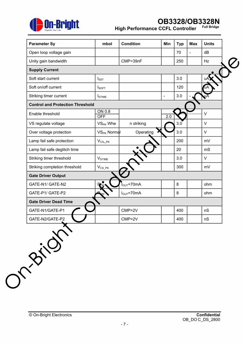
General Description The OB3328 is a unique, high-efficiency and high- precision Cold Cathode Fluorescent Lamp (CCFL) backlight co ntroller IC d edicated to full bridg e configuration. The controller i s de signed to drive single or multiple CCF Ls in Liquid Crystal Display (LCD) applications.
The OB332 8 convert s unre gulated DC input voltage to the pure sin usoidal voltage and cu rrent waveforms i n requi red freque ncy, to ignite and operate CCFL lamps.
The OB332 8 provides a high deg ree of design flexibility by offering great program mability for key parameters which incl ude operating frequency, striking frequ ency, st riking time, bu rst dimming frequency, soft-start time, and soft on/o ff time for burst dimming.
The OB3328 offers variab le dimming mode s and selectable di mming pol arity1. Both internal burs t and externa l low frequ ency PWM (LPWM) dimming methods are available for a wide range of dimming control (10% to 100%). Fu rthermore, analog dimmi ng is provide d thro ugh external DC input control to achi eve 40% to 100 % dimmin g range.
The highly integrated OB3 328 provides complete protection fe atures covering IC un der voltage lockout (UVL O), output o ver voltage prote ction, and lamp fail safe function.
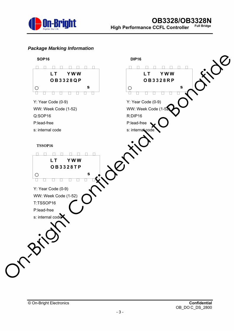
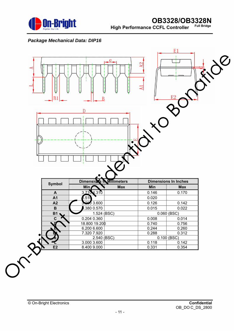
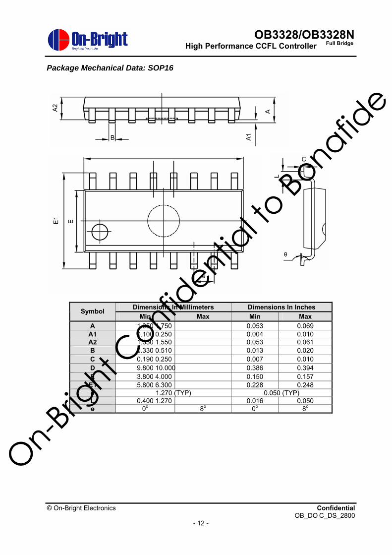
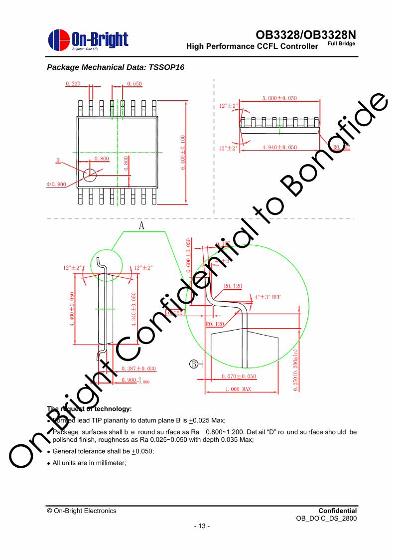
The OB3328 is available i n DIP-16, S OP-16 and TSSOP-16 Packages.
Features Support wide input voltage Full bridge topology High precision reference and frequency control Built-in peak detect circuit reduces BOM count Support single or multi-lamp applications High flexibility of dimming configuration: Analog Dimming Internal/external burst (PWM) mode dimming Concurrent burst and analog dimming control
Flexible user programmability: Operating frequency Striking frequency, striking voltage and time Soft start and soft on/off time Internal burst mode frequency
Comprehensive protection coverage: IC supply under voltage lockout (UVLO) Output over voltage protection (OVP) Lamp fail safe function
Applications Notebook computer LCD Monitor LCD TV LCD flat panel display for Instrument, automobile and handhold device
1 The OB3328 is with positive dimming polarity while its counter part OB3328N is in negative dimming polarity.
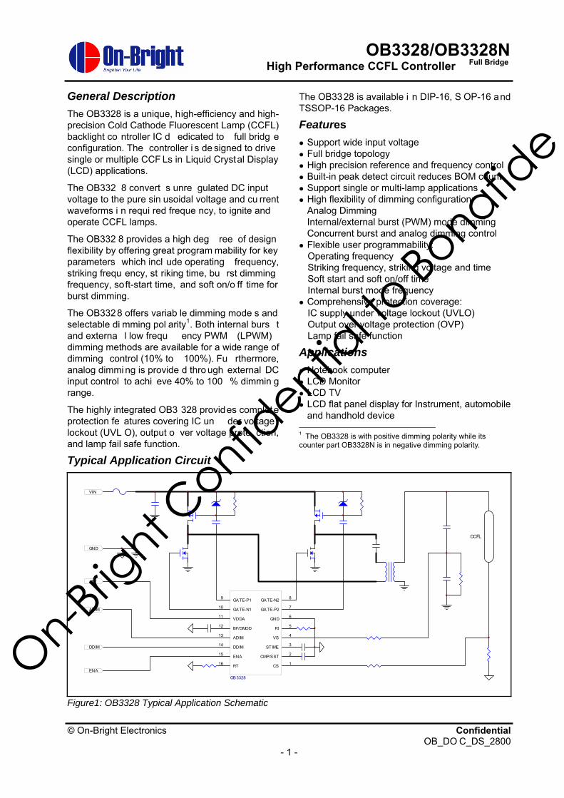
Typical Application Circuit
VIN
+5V
ENA
ADIM
CCFL
GND
CS 1CMP/SST 2
ST IME 3
VS 4
RI 5
GND 6
GATE-P2 7
GATE-N2 8GATE-P19
GATE-N110
VDDA11
BF/DMOD12
ADIM13
DDIM14
ENA15
RT16
OB3328
DDIM
Figure1: OB3328 Typical Application Schematic
On-Bright C
onfidentia
l to Bonafid
e
OB3328/OB3328NHigh Performance CCFL Controller Full Bridge
Absolute Maximum Ratings Parameter Value VDDA Input Voltage to GND 7V
I/O to GND -0.3 to VDDA + 0.3V
Operating Ambient Temperature TA
-20 to 85oC
Operating Junction Temperature TJ
150oC
Min/Max Storage Temperature Tstg
-55 to 150oC
Lead Temperature (10 Sec) 260 oC
Note: Stresses beyond those listed under “absolute maximum ratings” ma y ca use perman ent damage to the device. These are stress ratings onl y, fu nctional operation of th e device at these or an y ot her conditions be yond those ind icated under “recommended operating conditions” is not implied. Exposur e to absolute maximum-rated con ditions for exten ded periods may affect device reliability.
Recommended Operating Range Parameter Value VDDA Voltage 4.5V to 5.5V Operating Frequency 30 to 150KHz
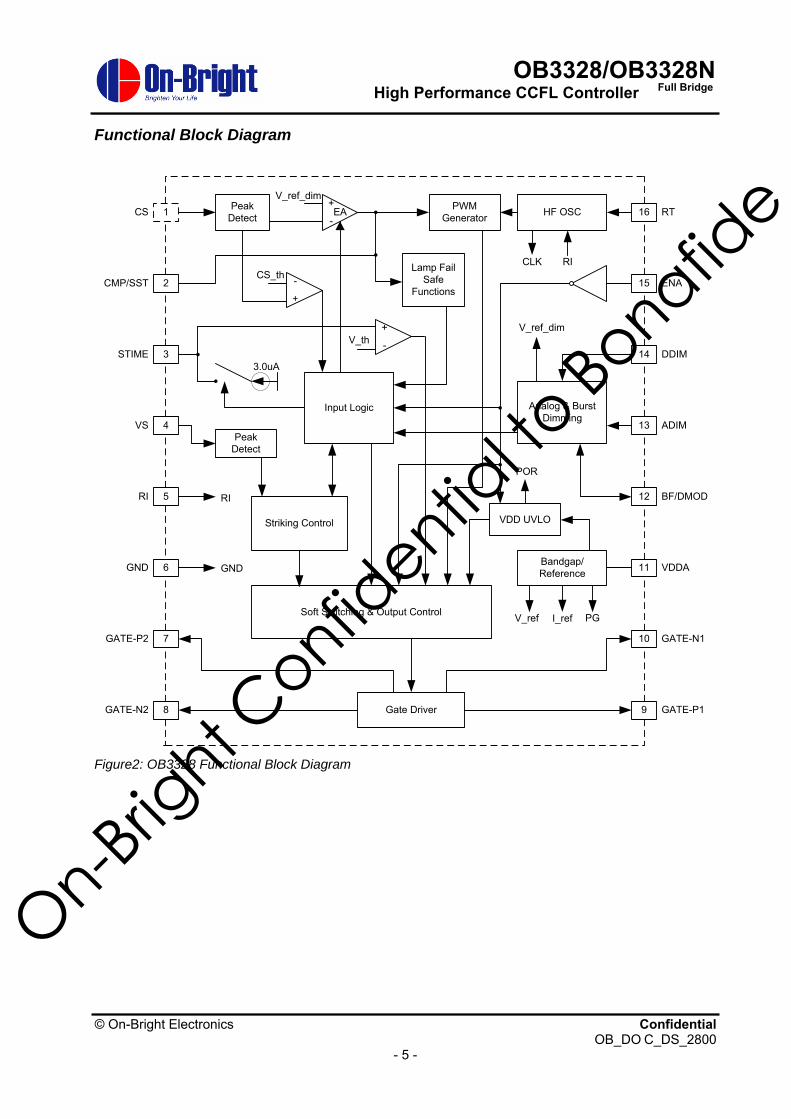
The OB3328 CCFL controller is designed to drive the inverter system in full bridge top ology, the resonant mo de full b ridge switche s conve rts unregulated DC voltage to pure sinusoidal waveforms for CCFL operating with high efficiency and low EMI emission. The resonant frequency of the tank i s set by th e tran sformer lea kage inductance, prima ry seri es capacitor and secondary parallel capacitor.
The OB3328 provides a high performance solution with a low system cost. One reference designs for single lamp appli cation is shown in figure 3 o n page 9.
Enable the Controller
OB3328 is activated by a pplying logic high to the ENA input. Control i s TTL logic compatible. The controller is enabled when the voltage at ENA pin is highe r than 1.1V. Toggling the ENA sign al resets the state machi ne hen ce restart s the inverter system.
Lamp Ignition and Striking Voltage Regulation
A much higher voltag e than that in normal operation is required to ignite CCFL, especially for aged la mp o r in low ambiance tempe rature. The programmable stri king freque ncy, vol tage an d ignition time set by RT, RI, VS, and STIME pins ensure suffici ent voltage and time fo r a ny CCFL ignition. RI in paralleled with RT pin is u sed to set the oscillator frequency which is close to resonant frequency of the tank at ignition stage thus provide sufficient stri king voltage. The output voltage is divided by the cap acitive voltage divider (forme d by C12 and C13 shown in figure 3 on page 9). The divided sig nal is fed into VS pin and its pea k is compared wi th internal 3.0V threshol d voltage. Consequently, the output voltage is regu lated and limited. The stri king voltage can be ap proximated as:
12•213•0.3
≈CCV
Vstriking
Once the out put voltage reache s the target level, and if CS pin voltage is le ss than 350mV, the IC will initiate the stri king timer. An internal constant 3.0uA current source starts to charge the capacitor connected to STIME pin. Voltage higher than 3.0V at STIME pin indicates an ignition timeout. Under such cir cumstance, P WM Gat e out puts are disabled and thus power s witches are turned off.
No energy is further delivered to the CCFL load.
Voltage at CS pin greater than 300mV indicates the lamp being ignited and capacitor at STIME pin will be discha rged. Capacitor in app ropriate value is req uired to provide sufficient time (typically, 1 second) to ignite the lamp. Ignition time is approximated as:
C[uF]=T(sec)
Over Voltage Protection
During n ormal ope rating, if VS peak voltag e reaches the internal threshold of 3.0V, the controller im mediately sh uts do wn th e inverte r. OVP is a latch shutd own and could only be re set by toggling ENA pin.
Soft Start and Soft On/off
External ca pacitor connected to CM P/SST pin provides soft start and soft on/off control. At start up, an internal current source starts to charge the capacitor. Consequently, voltage at CM P/SST pin increases gradually and so as to the overlap tim e of the PWM Gate si gnals. This soft st art control helps to redu ce the MOS FET inru sh current an d voltage stre sses, thus expand the lam p life. The slope of the soft st art TV Δ/Δ can be approximated as:
RT[kohm]C36103=
TV -6
×××
ΔΔ
Once lamps are ignited, the ca pacitor connected to CMP/SST pin performs the loop com pensation function. In intern al bu rst m ode dimming o r external b urst (PWM) mo de dimmi ng conditions, the voltage rampi ng up and do wn a t this pin performs a soft on/off control function in each burst cycle.
Normal Operation and Striking Frequency
The ope ration freque ncy is determi ned by the external resi stor con nected to RT pin. The operation frequency is calculated by th e following equation:
RT(Kohm)1800=(KHz)Fop
At ignition st age, RI pi n is internally connected to RT pin, there fore external resistor at RI pin is in parallel with the external resi stor at RT pin. The striking fre quency can be cal culated by the
On-Bright C
onfidentia
l to Bonafid
e
OB3328/OB3328NHigh Performance CCFL Controller Full Bridge
The lamp cu rrent is regul ated by a la mp curren t feedback loo p with an i nternal transconductance error amplifier, the AC lamp current is sensed by a sense resistor (R1 3 in figure 3 on page 9) connected in series with t he low voltage terminal of CCFL la mp. The AC voltage a cross the sen se resistor is fed into the CS pin. The peak voltage of sensed AC voltage is detected and compared with a 1.25V internal refe rence voltage. The error is amplified that controls the on time of the full bridge switches, as a result, the lamp current is regulated. the lamp current can be calculated by the following equation:
senselamp R
VI•
=2
25.1
Lamp Fail Safe Functions
During normal operation, if the lamp is removed or damaged, the voltage at CS pin will drops to 0V. If the peak voltage at CS pin cannot be regulated to the predetermined value for more than 20ms, the inverter i s l atched shut down. Toggl ing ENA restarts the operation.
Dimming Control
Three com monly used di mming mod es: analo g mode dimming, internal b urst mode dimming and external b urst (PWM ) d imming fun ctions a re supported without any additional components. The concurrent a nalog and b urst a chieves very wid e dimming range.
DC volta ge ranging from 0V to 3V at ADIM pin performs a nalog mod e dimming control. The voltage at ADIM pin modulates i nternal error amplifier reference voltag e from 0.5V to 1.25V, witch corresponds to a lamp current o f approximately 40% to 100%.
The BF/DM OD pin is u sed for internal/external burst mode selection and internal burst frequency setting. External bu rst (P WM) dimming mod e is selected by shorting BF/DMOD pin to ground. The OB3328 accepts an external low f requency PWM (LPWM) signal to DDIM pin with a voltage swinging fro m less th an 0.8V to that of greate r than 2.0V. The lamp brightness is controlled by the duty cycle of the LPWM sign al. T he bu rst
frequency is equal to LPWM frequency.
Internal bu rst mode dimming is obt ained by connecting a c apacitor to BF/DMOD pin. A low frequency triangular waveform generator is formed by the ca pacitor alon g wit h intern al co mparator, internal current sou rce and current sink. Th e triangular voltage waveform with p eak of 3V and valley of 1V at this pi n is used for the internal low frequency burst PWM generation. its duty cycle so as to lamp cu rrent is controlled by the DC volt age at DDIM pin. The burst freque ncy F burst is set by the following equation:
)nF(C2000
=)Hz(FBF
burst
A DC voltage rangin g from 0V to 3V at DIM pin corresponds to a lamp c urrent of approximately 10% to 100%.
PIN\MODE Analog Internal Burst
External LPWM
BF/DMOD - Capacitor <0.5V
DDIM - 0-3V External LPWM
ADIM 0-3V - -
The concurrent burst and analog dimming control can achieves approximately 4% to 100% dimming ratio.
On-Bright C
onfidentia
l to Bonafid
e
OB3328/OB3328NHigh Performance CCFL Controller Full Bridge
Formed lead TIP planarity to datum plane B is +0.025 Max;
Package surfaces shall b e round su rface as Ra 0.800~1.200. Det ail “D” ro und su rface sho uld be polished finish, roughness as Ra 0.025~0.050 with depth 0.035 Max;
General tolerance shall be +0.050;
All units are in millimeter;
On-Bright C
onfidentia
l to Bonafid
e
OB3328/OB3328NHigh Performance CCFL Controller Full Bridge
On-Bright El ectronics Corp. re serves the right t o make correction s, mod ifications, en hancements, improvements, and other changes to its products and services at any time and to discontinue any product or service without notice. Customers should obt ain the latest relevant information before placing orders and should verify that such information is current and complete.
Warranty information
On-Bright Electronics Corp. warrants performance of its hardware products to the specifications applicable at the time of sale in acco rdance with its standard warranty. Testing and other quality contro l techniques are u sed to the extent it deems necessary to s upport this warra nty. Except whe re mandate d by government requirements, testing of all parameters of each product is not necessarily performed.
On-Bright Electronics Corp. assumes no liability for applications assist ance or customer product design. Customers are responsible for their products and applications using On-Bright’s components, data sheet and ap plication note s. T o minimize th e risks asso ciated with cu stomer products and appli cations, customers should provide adequate design and operating safeguards.
Life support
On-Bright Electronics Corp.’s products are not designed to be used as components in devices intended to support or sustain human life. On-bright Electronics Corp. will not be held liable for any damages or claims resulting from the use of its products in medical applications.
Military
On-Bright El ectronics Corp.’s products a re n ot d esigned fo r use i n milit ary appli cations. O n-Bright Electronics Corp. will not be held liable for any damages or claims resulting from the use of its products in military applications.