May 2009 Doc ID 9685 Rev 7 1/272 1 UPSD33xx Turbo series fast 8032 MCU with programmable logic Features ■ Fast 8-bit Turbo 8032 MCU, 40 MHz – Advanced core, 4-clocks per instruction – 10 MIPs, peak performance at 40 MHz (5 V) – JTAG debug and in-system programming – Branch cache and6 instruction prefetch queue – Dual XDATA pointers with auto increment and decrement – Compatible with 3rd party 8051 tools ■ Dual Flash memories with memory management – Place either memory into 8032 program address space or data address space – Read-while-write operation for in- application programming and EEPROM emulation – Single voltage program and erase – 100K guaranteed erase cycles, 15-year retention ■ Clock, reset, and supply management – Flexible 8-level CPU clock divider register – Normal, Idle, and Power-down modes – Power-on and low voltage reset supervisor – Programmable watchdog timer ■ Programmable logic, general purpose – 16 macrocells – Create shifters, state machines, chip- selects, glue-logic to keypads, panels, LCDs, others ■ Packages are ECOPACK ® ■ Communication interfaces – I 2 C master/slave controller, 833 kHz – SPI master controller, 10 MHz – Two UARTs with independent baud rate – IrDA protocol support up to 115 Kbaud – Up to 46 I/O, 5 V tolerant on 3.3 V UPSD33xxV ■ A/D converter – Eight channels, 10-bit resolution, 6 μs ■ Timers and interrupts – Three 8032 standard 16-bit timers – Programmable counter array (PCA), six 16- bit modules for PWM/CAPCOM/timers – 8/10/16-bit PWM operation – 11 interrupt sources with two external interrupt pins ■ Operating voltage source (±10%) – 5 V devices use both 5.0 V and 3.3 V – 3.3 V devices use only 3.3 V source Table 1. Device summary LQFP52 (T) 52-lead, thin, quad, Flat LQFP80 (U) 80-lead, thin, quad, flat Reference Part number UPSD33xx UPSD3312D, UPSD3333D, UPSD3334D, UPSD3354D UPSD3312DV, UPSD3333DV, UPSD3334DV, UPSD3354DV www.st.com Obsolete Product(s) - Obsolete Product(s) Obsolete Product(s) - Obsolete Product(s)
Transcript
May 2009 Doc ID 9685 Rev 7 1/272
1
UPSD33xxTurbo series
fast 8032 MCU with programmable logic
Features■ Fast 8-bit Turbo 8032 MCU, 40 MHz
– Advanced core, 4-clocks per instruction– 10 MIPs, peak performance at 40 MHz
and decrement– Compatible with 3rd party 8051 tools
■ Dual Flash memories with memory management– Place either memory into 8032 program
address space or data address space– Read-while-write operation for in-
application programming and EEPROM emulation
– Single voltage program and erase– 100K guaranteed erase cycles, 15-year
retention
■ Clock, reset, and supply management– Flexible 8-level CPU clock divider register– Normal, Idle, and Power-down modes– Power-on and low voltage reset supervisor– Programmable watchdog timer
■ Programmable logic, general purpose– 16 macrocells– Create shifters, state machines, chip-
selects, glue-logic to keypads, panels, LCDs, others
■ Packages are ECOPACK®
■ Communication interfaces– I2C master/slave controller, 833 kHz– SPI master controller, 10 MHz– Two UARTs with independent baud rate– IrDA protocol support up to 115 Kbaud– Up to 46 I/O, 5 V tolerant on 3.3 V
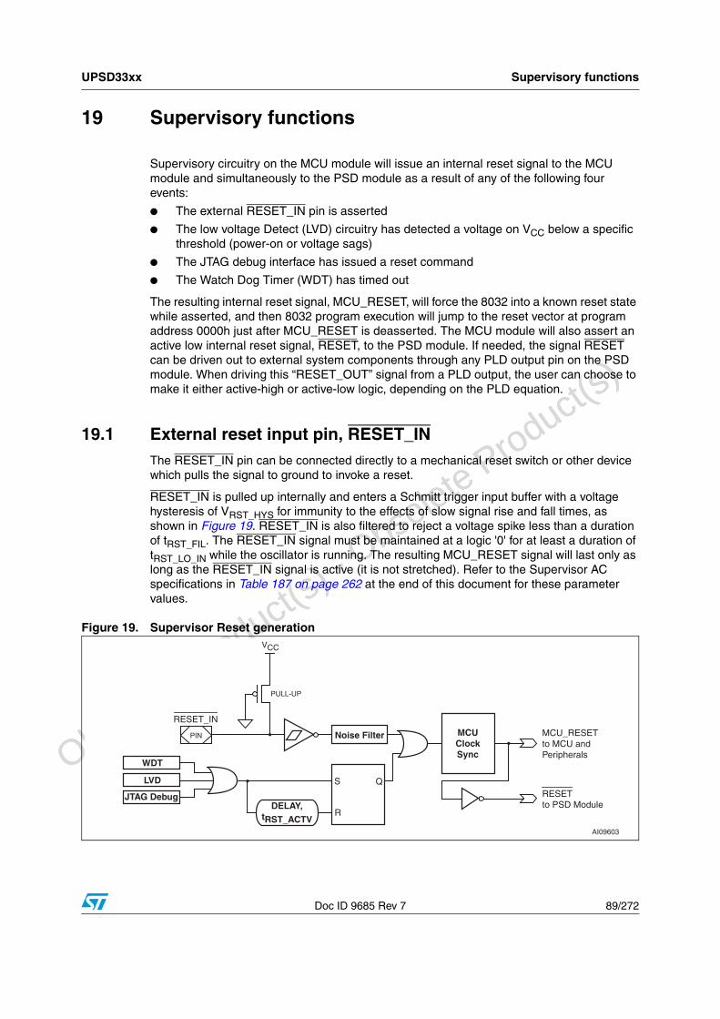
The Turbo UPSD33xx series combines a powerful 8051-based microcontroller with a flexible memory structure, programmable logic, and a rich peripheral mix to form an ideal embedded controller. At its core is a fast 4-cycle 8032 MCU with a 6-byte instruction prefetch queue (PFQ) and a 4-entry fully associative branching cache (BC) to maximize MCU performance, enabling loops of code in smaller localities to execute extremely fast.
Code development is easily managed without a hardware in-circuit emulator by using the serial JTAG debug interface. JTAG is also used for in-system programming (ISP) in as little as 10 seconds, perfect for manufacturing and lab development. The 8032 core is coupled to programmable system device (PSD) architecture to optimize the 8032 memory structure, offering two independent banks of Flash memory that can be placed at virtually any address within 8032 program or data address space, and easily paged beyond 64 Kbytes using on-chip programmable decode logic. Dual Flash memory banks provide a robust solution for remote product updates in the field through in-application programming (IAP). Dual Flash banks also support EEPROM emulation, eliminating the need for external EEPROM chips. General purpose programmable logic (PLD) is included to build an endless variety of glue-logic, saving external logic devices. The PLD is configured using the software development tool, PSDsoft™ Express, available from the web at www.st.com, at no charge. The UPSD33xx also includes supervisor functions such as a programmable watchdog timer and low-voltage reset.
Obsolete Product(
s) - O
bsolete Product(
s)
Obsolete Product(
s) - O
bsolete Product(
s)
UPSD33xx Description
Doc ID 9685 Rev 7 19/272
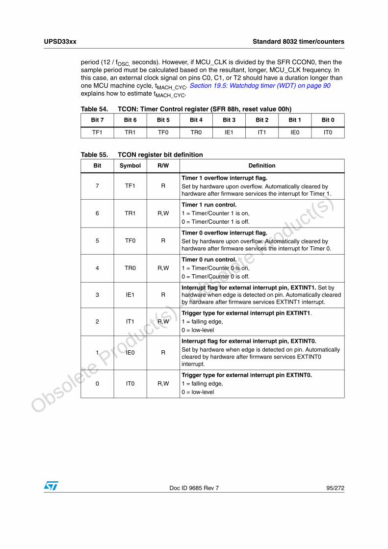
Figure 1. Block diagram
PA0:7
PB0:7
PD1:2
PC0:7
MCUBus
P4.0:7
P1.0:7
P3.0:7
UPSD33xx
SY
ST
EM
BU
S
DedicatedPins
Supervisor:Watchdog and Low-Voltage Reset
1st Flash Memory:64K, 128K,
or 256K Bytes
2nd Flash Memory:16K or 32K Bytes
SRAM:2K, 8K, or 32K Bytes
ProgrammableDecode andPage Logic
GeneralPurpose
ProgrammableLogic,
16 Macrocells
(8) GPIO, Port A(80-pin only)
(8) GPIO, Port B
(4) GPIO, Port C
(2) GPIO, Port D
JTAG ICE and ISP
8032 Address/Data/Control Bus(80-pin device only)
VCC, VDD, GND, Reset, Crystal In
Turbo8032Core
PFQ&
BC
(3) 16-bitTimer/
Counters
(2)ExternalInterrupts
I2C
SPI
(8) 10-bit ADC
UART0
(8) GPIO, Port 1
(8) GPIO, Port 3
(8) GPIO, Port 4
UART1Optional IrDA
Encoder/Decoder
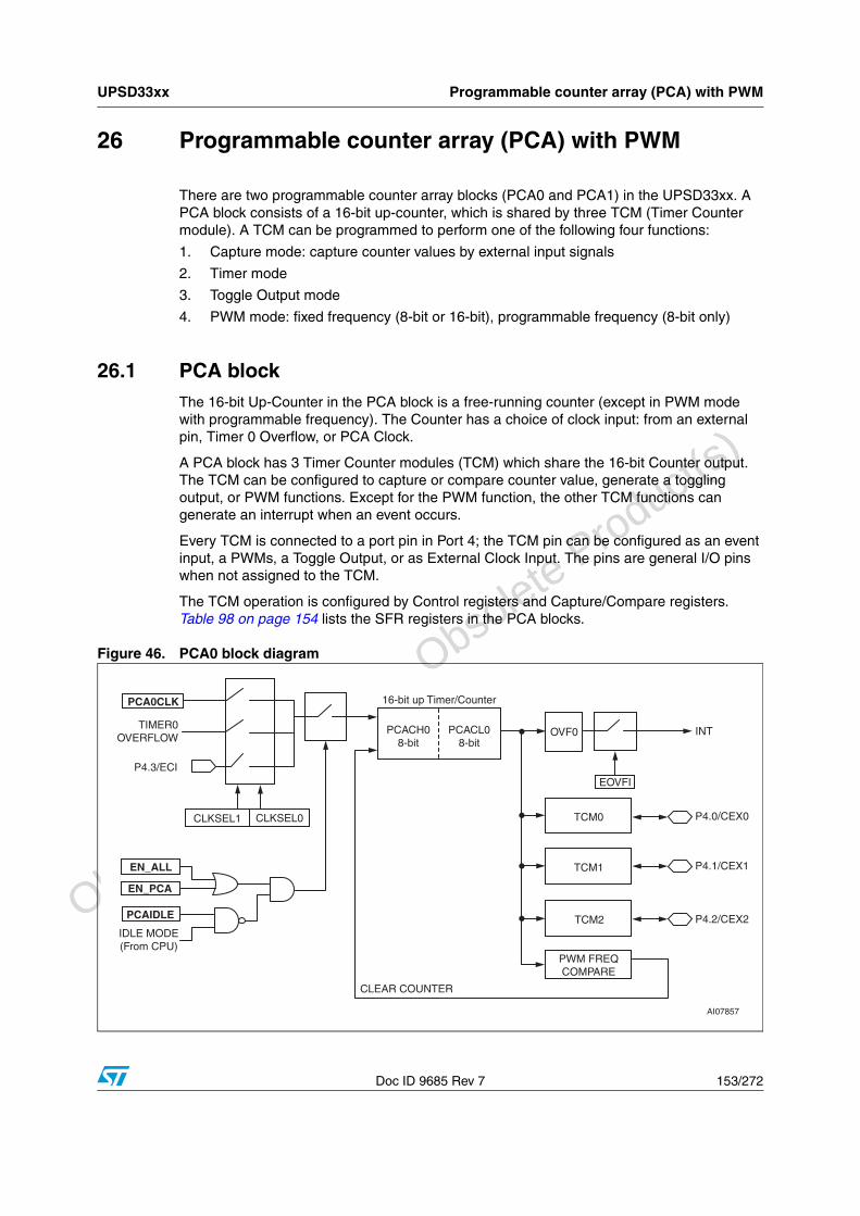
16-bit PCA(6) PWM, CAPCOM, TIMER
AI08875b
Obsolete Product(
s) - O
bsolete Product(
s)
Obsolete Product(
s) - O
bsolete Product(
s)
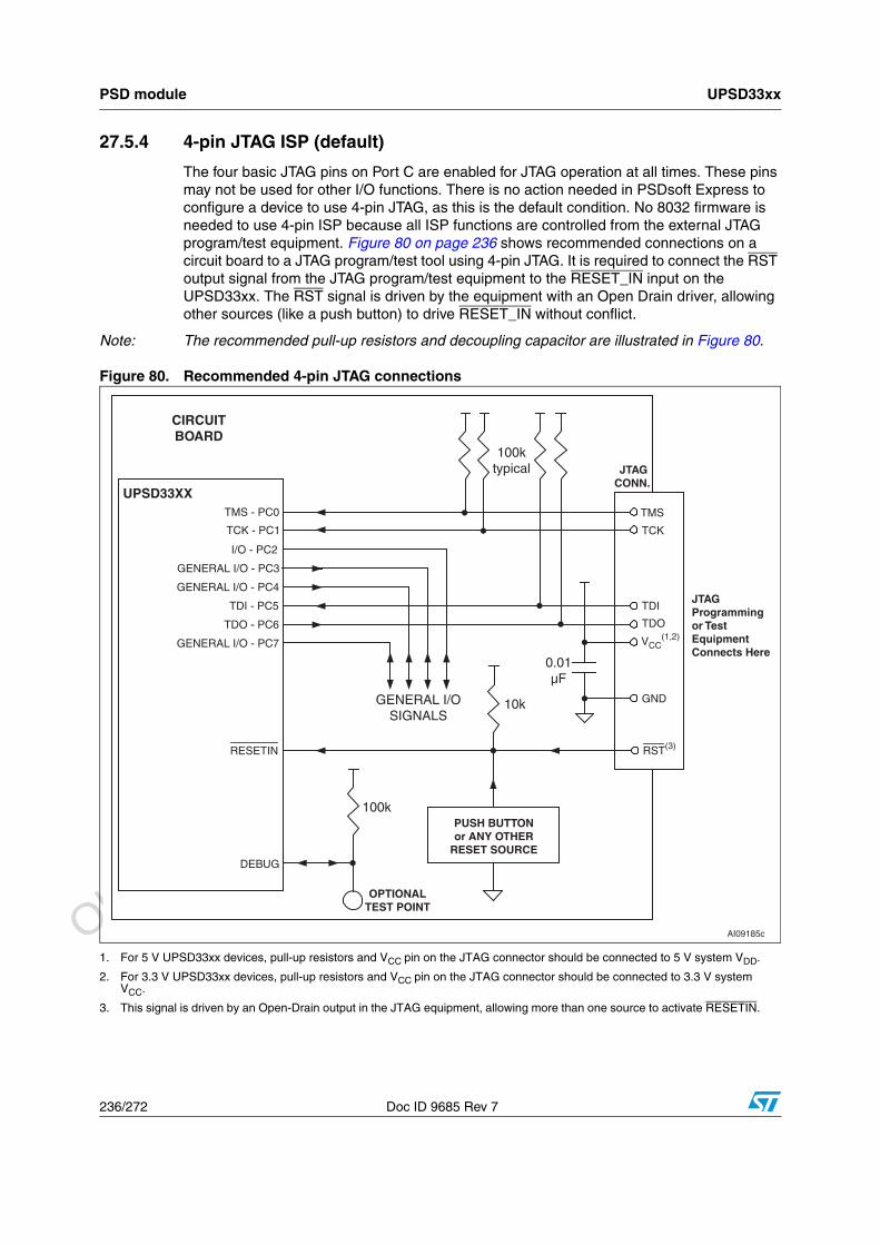
Pin descriptions UPSD33xx
20/272 Doc ID 9685 Rev 7
2 Pin descriptions
Figure 2. LQFP52 connections
1. For 5 V applications, VDD must be connected to a 5.0 V source. For 3.3 V applications, VDD must be connected to a 3.3 V source.
2. These signals can be used on one of two different ports (Port 1 or Port 4) for flexibility. Default is Port1.
3. AVREF and 3.3 V AVCC are shared in the 52-pin package only. ADC channels must use AVCC as AVREF for the 52-pin package.
39 P1.5/SPIRXD(2)/ADC5
38 P1.4/SPICLK(2)/ADC4
37 P1.3/TXD1(IrDA)(2)/ADC3
36 P1.2/RXD1(IrDA)(2)/ADC2
35 P1.1/T2X(2)/ADC1
34 P1.0/T2(2)/ADC0
33 VDD(1)
32 XTAL2
31 XTAL1
30 P3.7/SCL
29 P3.6/SDA
28 P3.5/C1
27 P3.4/C0
PD1/CLKIN
PC7
JTAG TDO
JTAG TDI
DEBUG
3.3V VCC
PC4/TERR
VDD(1)
GND
PC3/TSTAT
PC2
JTAG TCK
JTAG TMS
1
2
3
4
5
6
7
8
9
10
11
12
13
52 51 50 49 48 47 46 45 44 43 42 41 40
PB
0
PB
1
PB
2
PB
3
PB
4
AV
CC
/AV
RE
F(3
)
PB
5
GN
D
RE
SE
T_I
N
PB
6
PB
7
P1.
7/S
PIS
EL(
2)/A
DC
7
P1.
6/S
PIT
XD
(2) /A
DC
6
14 15 16 17 18 19 20 21 22 23 24 25 26
SP
ISE
L(2)
/PC
AC
LK1/
P4.
7
SP
ITX
D(2
) /TC
M5/
P4.
6
SP
IRX
D(2
) /TC
M4/
P4.
5
SP
ICLK
(2) /T
CM
3/P
4.4
TX
D1(
IrD
A)(
2)/P
CA
CLK
0/P
4.3
GN
D
RX
D1(
IrD
A)(
2)/T
CM
2/P
4.2
T2X
(2) /T
CM
1/P
4.1
T2(
2)/T
CM
0/P
4.0
RX
D0/
P3.
0
TX
D0/
P3.
1
EX
TIN
T0/
TG
0/P
3.2
EX
TIN
T1/
TG
1/P
3.3
AI07822b
Obsolete Product(
s) - O
bsolete Product(
s)
Obsolete Product(
s) - O
bsolete Product(
s)
UPSD33xx Pin descriptions
Doc ID 9685 Rev 7 21/272
Figure 3. LQFP80 connections
1. For 5 V applications, VDD must be connected to a 5.0 V source. For 3.3 V applications, VDD must be connected to a 3.3 V source.
2. These signals can be used on one of two different ports (Port 1 or Port 4) for flexibility. Default is Port1.
MCUAD1 AD1 37 N/A I/OMultiplexed address/data bus A1/D1
MCUAD2 AD2 38 N/A I/OMultiplexed address/data bus A2/D2
MCUAD3 AD3 39 N/A I/OMultiplexed address/data bus A3/D3
MCUAD4 AD4 41 N/A I/OMultiplexed address/data bus A4/D4
MCUAD5 AD5 43 N/A I/OMultiplexed address/data bus A5/D5
MCUAD6 AD6 45 N/A I/OMultiplexed address/data bus A6/D6
MCUAD7 AD7 47 N/A I/OMultiplexed address/data bus A7/D7
MCUA8 A8 51 N/A OExternal bus, Addr A8
MCUA9 A9 53 N/A OExternal bus, Addr A9
MCUA10 A10 55 N/A OExternal bus, Addr A10
MCUA11 A11 57 N/A OExternal bus, Addr A11
P1.0T2
ADC052 34 I/O
General I/O port pin
Timer 2 Count input (T2)
ADC Channel 0 input (ADC0)
P1.1T2X
ADC154 35 I/O
General I/O port pin
Timer 2 Trigger input (T2X)
ADC Channel 1 input (ADC1)
P1.2RxD1 ADC2
56 36 I/OGeneral I/O port pin
UART1 or IrDA Receive (RxD1)
ADC Channel 2 input (ADC2)
P1.3TXD1 ADC3
58 37 I/OGeneral I/O port pin
UART or IrDA Transmit (TxD1)
ADC Channel 3 input (ADC3)
Obsolete Product(
s) - O
bsolete Product(
s)
Obsolete Product(
s) - O
bsolete Product(
s)
UPSD33xx Pin descriptions
Doc ID 9685 Rev 7 23/272
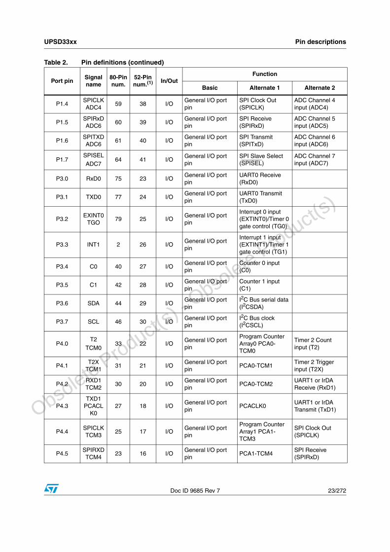
P1.4SPICLK ADC4
59 38 I/OGeneral I/O port pin
SPI Clock Out (SPICLK)
ADC Channel 4 input (ADC4)
P1.5SPIRxD ADC6
60 39 I/OGeneral I/O port pin
SPI Receive (SPIRxD)
ADC Channel 5 input (ADC5)
P1.6SPITXD ADC6
61 40 I/OGeneral I/O port pin
SPI Transmit (SPITxD)
ADC Channel 6 input (ADC6)
P1.7SPISEL
ADC764 41 I/O
General I/O port pin
SPI Slave Select (SPISEL)
ADC Channel 7 input (ADC7)
P3.0 RxD0 75 23 I/OGeneral I/O port pin
UART0 Receive (RxD0)
P3.1 TXD0 77 24 I/OGeneral I/O port pin
UART0 Transmit (TxD0)
P3.2EXINT0
TGO79 25 I/O
General I/O port pin
Interrupt 0 input (EXTINT0)/Timer 0 gate control (TG0)
P3.3 INT1 2 26 I/OGeneral I/O port pin
Interrupt 1 input (EXTINT1)/Timer 1 gate control (TG1)
P3.4 C0 40 27 I/OGeneral I/O port pin
Counter 0 input (C0)
P3.5 C1 42 28 I/OGeneral I/O port pin
Counter 1 input (C1)
P3.6 SDA 44 29 I/OGeneral I/O port pin
I2C Bus serial data (I2CSDA)
P3.7 SCL 46 30 I/OGeneral I/O port pin
I2C Bus clock (I2CSCL)
P4.0T2
TCM033 22 I/O
General I/O port pin
Program Counter Array0 PCA0-TCM0
Timer 2 Count input (T2)
P4.1T2X
TCM131 21 I/O
General I/O port pin
PCA0-TCM1Timer 2 Trigger input (T2X)
P4.2RXD1 TCM2
30 20 I/OGeneral I/O port pin
PCA0-TCM2UART1 or IrDA Receive (RxD1)
P4.3TXD1
PCACLK0
27 18 I/OGeneral I/O port pin
PCACLK0UART1 or IrDA Transmit (TxD1)
P4.4SPICLK TCM3
25 17 I/OGeneral I/O port pin
Program Counter Array1 PCA1-TCM3
SPI Clock Out (SPICLK)
P4.5SPIRXD TCM4
23 16 I/OGeneral I/O port pin
PCA1-TCM4SPI Receive (SPIRxD)
Table 2. Pin definitions (continued)
Port pinSignal name
80-Pin num.
52-Pin num.(1) In/Out
Function
Basic Alternate 1 Alternate 2
Obsolete Product(
s) - O
bsolete Product(
s)
Obsolete Product(
s) - O
bsolete Product(
s)
Pin descriptions UPSD33xx
24/272 Doc ID 9685 Rev 7
P4.6SPITXD
TCM519 15 I/O
General I/O port pin
PCA1-TCM5SPI Transmit (SPITxD)
P4.7SPISEL
PCACLK1
18 14 I/OGeneral I/O port pin
PCACLK1SPI Slave Select (SPISEL)
AVREF 70 N/A I
Reference voltage input for ADC. Connect AVREF to VCC if the ADC is not used.
RD 65 N/A OREAD Signal, external bus
WR 62 N/A OWRITE Signal, external bus
PSEN 63 N/A OPSEN Signal, external bus
ALE 4 N/A OAddress Latch signal, external bus
RESET_IN 68 44 IActive low reset input
XTAL1 48 31 IOscillator input pin for system clock
XTAL2 49 32 OOscillator output pin for system clock
DEBUG 8 5 I/OI/O to the MCU debug unit
Table 2. Pin definitions (continued)
Port pinSignal name
80-Pin num.
52-Pin num.(1) In/Out
Function
Basic Alternate 1 Alternate 2
Obsolete Product(
s) - O
bsolete Product(
s)
Obsolete Product(
s) - O
bsolete Product(
s)
UPSD33xx Pin descriptions
Doc ID 9685 Rev 7 25/272
PA0 35 N/A I/OGeneral I/O port pin
All Port A pins support:– PLD Macro-cell
outputs, or– PLD inputs, or
– Latched Address Out (A0-A7), or
– Peripheral I/O mode
PA1 34 N/A I/OGeneral I/O port pin
PA2 32 N/A I/OGeneral I/O port pin
PA3 28 N/A I/OGeneral I/O port pin
PA4 26 N/A I/OGeneral I/O port pin
PA5 24 N/A I/OGeneral I/O port pin
PA6 22 N/A I/OGeneral I/O port pin
PA7 21 N/A I/OGeneral I/O port pin
1. N/A = Signal Not Available on 52-pin package.
Table 2. Pin definitions (continued)
Port pinSignal name
80-Pin num.
52-Pin num.(1) In/Out
Function
Basic Alternate 1 Alternate 2
Obsolete Product(
s) - O
bsolete Product(
s)
Obsolete Product(
s) - O
bsolete Product(
s)
UPSD33xx hardware description UPSD33xx
26/272 Doc ID 9685 Rev 7
3 UPSD33xx hardware description
The UPSD33xx has a modular architecture built from a stacked die process. There are two die, one is designated “MCU module” in this document, and the other is designated “PSD module” (see Figure 4 on page 27). In all cases, the MCU module die operates at 3.3 V with 5 V tolerant I/O. The PSD module is either a 3.3 V die or a 5 V die, depending on the UPSD33xx device as described below.
The MCU module consists of a fast 8032 core, that operates with 4 clocks per instruction cycle, and has many peripheral and system supervisor functions. The PSD module provides the 8032 with multiple memories (two Flash and one SRAM) for program and data, programmable logic for address decoding and for general-purpose logic, and additional I/O. The MCU module communicates with the PSD module through internal address and data busses (A8 – A15, AD0 – AD7) and control signals (RD, WR, PSEN, ALE, RESET).
There are slightly different I/O characteristics for each module. I/Os for the MCU module are designated as Ports 1, 3, and 4. I/Os for the PSD module are designated as Ports A, B, C, and D.
For all 5 V UPSD33xx devices, a 3.3 V MCU module is stacked with a 5 V PSD module. In this case, a 5 V UPSD33xx device must be supplied with 3.3 VCC for the MCU module and 5.0VDD for the PSD module. Ports 3 and 4 of the MCU module are 3.3 V ports with tolerance to 5 V devices (they can be directly driven by external 5 V devices and they can directly drive external 5 V devices while producing a VOH of 2.4 V min and VCC max). Ports A, B, C, and D of the PSD module are true 5 V ports.
For all 3.3 V UPSD33xxV devices, a 3.3 V MCU module is stacked with a 3.3 V PSD module. In this case, a 3.3 V UPSD33xx device needs to be supplied with a single 3.3 V voltage source at both VCC and VDD. I/O pins on Ports 3 and 4 are 5 V tolerant and can be connected to external 5 V peripherals devices if desired. Ports A, B, C, and D of the PSD module are 3.3 V ports, which are not tolerant to external 5 V devices.
Refer to Table 3 on page 27 for port type and voltage source requirements.
80-pin UPSD33xx devices provide access to 8032 address, data, and control signals on external pins to connect external peripheral and memory devices. 52-pin UPSD33xx devices do not provide access to the 8032 system bus.
All non-volatile memory and configuration portions of the UPSD33xx device are programmed through the JTAG interface and no special programming voltage is needed. This same JTAG port is also used for debugging of the 8032 core at runtime providing breakpoint, single-step, display, and trace features. A non-volatile security bit may be programmed to block all access via JTAG interface for security. The security bit is defeated only by erasing the entire device, leaving the device blank and ready to use again.
Obsolete Product(
s) - O
bsolete Product(
s)
Obsolete Product(
s) - O
bsolete Product(
s)
UPSD33xx UPSD33xx hardware description
Doc ID 9685 Rev 7 27/272
Table 3. Port type and voltage source combinations
Figure 4. UPSD33xx functional modules
Device TypeVCC for MCU
moduleVDD for PSD
modulePorts 3 and 4 on
MCU modulePorts A, B, C, and D
on PSD module
5 V:
UPSD33xx3.3 V 5.0 V 3.3 V but 5 V tolerant 5 V
3.3 V:
UPSD33xxV3.3 V 3.3 V 3.3 V but 5 V tolerant 3.3 V. NOT 5 V tolerant
10-bitADC
Dedicated MemoryInterface Prefetch,
Branch Cache
Enhanced MCU Interface
Decode PLDPSD Page Register SRAM
CPLD - 16 MACROCELLSJTAG ISP
Reset LogicWDT
InternalReset
Port 1Port 3
DualUARTs
Interrupt
3 Timer /Counters
256 Byte SRAM
Turbo 8032 Core
PSD Internal Bus
8032 Internal Bus
PSDReset
LVD
I2CUnit
Port DGPIO
Port CJTAG and
GPIO
SecondaryFlash
Reset Input
UPSD33XX
JTAGDEBUG
8-Bit Die-to-Die Bus
Main Flash
PCAPWM
Counters
ResetPin
Ext.Bus
SPI
VCC Pins3.3V
VDD Pins3.3V or 5V
MCU Module
PSD Module
Port 3 - UART0,Intr, Timers Port 1 - Timer, ADC, SPI
Port 4 - PCA,PWM, UART1
Port 3I2C
XTALClock Unit
Port A,B,C PLDI/O and GPIO
AI07842b
Obsolete Product(
s) - O
bsolete Product(
s)
Obsolete Product(
s) - O
bsolete Product(
s)
Memory organization UPSD33xx
28/272 Doc ID 9685 Rev 7
4 Memory organization
The 8032 MCU core views memory on the MCU module as “internal” memory and it views memory on the PSD module as “external” memory, see Figure 5
Internal memory on the MCU module consists of DATA, IDATA, and SFRs. These standard 8032 memories reside in 384 bytes of SRAM located at a fixed address space starting at address 0x0000.
External memory on the PSD module consists of four types: main Flash (64, 128, or 256 Kbytes), a smaller secondary Flash (16 or 32 Kbytes), SRAM (2, 8, or 32 Kbytes), and a block of PSD module control registers called CSIOP (256 bytes). These external memories reside at programmable address ranges, specified using the software tool PSDsoft Express. See the Section 27: PSD module on page 164 of this document for more details on these memories.
External memory is accessed by the 8032 in two separate 64 Kbyte address spaces. One address space is for program memory and the other address space is for data memory. Program memory is accessed using the 8032 signal, PSEN. Data memory is accessed using the 8032 signals, RD and WR. If the 8032 needs to access more than 64 Kbytes of external program or data memory, it must use paging (or banking) techniques provided by the Page register in the PSD module.
Note: When referencing program and data memory spaces, it has nothing to do with 8032 internal SRAM areas of DATA, IDATA, and SFR on the MCU module. Program and data memory spaces only relate to the external memories on the PSD module.
External memory on the PSD module can overlap the internal SRAM memory on the MCU module in the same physical address range (starting at 0x0000) without interference because the 8032 core does not assert the RD or WR signals when accessing internal SRAM.
Figure 5. UPSD33xx memories
• External memories may be placed at virtuallyany address using software tool PSDsoft Express.
• The SRAM and Flash memories may be placedin 8032 Program Space or Data Space usingPSDsoft Express.
• Any memory in 8032 Data Space is XDATA.
64KB,128KB,
or256KB
16KBor
32KB
MainFlash
Internal SRAM onMCU Module
External Memory onPSD Module
IDATA SFR
DATA
SecondaryFlash
2KB,8KB,
or32KB
SRAM
256 Bytes
CSIOP
384 Bytes SRAM
Direct or Indirect Addressing
FF
80
7F
128 Bytes
128 Bytes
128 Bytes
0
IndirectAddressing
FixedAddresses
DirectAddressing
AI07843
Obsolete Product(
s) - O
bsolete Product(
s)
Obsolete Product(
s) - O
bsolete Product(
s)
UPSD33xx Memory organization
Doc ID 9685 Rev 7 29/272
4.1 Internal memory (MCU, standard 8032 memory: DATA, IDATA, SFR)
4.1.1 DATA memory
The first 128 bytes of internal SRAM ranging from address 0x0000 to 0x007F are called DATA, which can be accessed using 8032 direct or indirect addressing schemes and are typically used to store variables and stack.
Four register banks, each with 8 registers (R0 – R7), occupy addresses 0x0000 to 0x001F. Only one of these four banks may be enabled at a time. The next 16 locations at 0x0020 to 0x002F contain 128 directly addressable bit locations that can be used as software flags. SRAM locations 0x0030 and above may be used for variables and stack.
4.1.2 IDATA memory
The next 128 bytes of internal SRAM are named IDATA and range from address 0x0080 to 0x00FF. IDATA can be accessed only through 8032 indirect addressing and is typically used to hold the MCU stack as well as data variables. The stack can reside in both DATA and IDATA memories and reach a size limited only by the available space in the combined 256 bytes of these two memories (since stack accesses are always done using indirect addressing, the boundary between DATA and IDATA does not exist with regard to the stack).
4.1.3 SFR memory
Special function registers (Table 5 on page 41) occupy a separate physical memory, but they logically overlap the same 128 bytes as IDATA, ranging from address 0x0080 to 0x00FF. SFRs are accessed only using direct addressing. There 86 active registers used for many functions: changing the operating mode of the 8032 MCU core, controlling 8032 peripherals, controlling I/O, and managing interrupt functions. The remaining unused SFRs are reserved and should not be accessed.
16 of the SFRs are both byte- and bit-addressable. Bit-addressable SFRs are those whose address ends in “0” or “8” hex.
4.2 External memory (PSD module: program memory, data memory)The PSD module has four memories: main Flash, secondary Flash, SRAM, and CSIOP. Section 27: PSD module on page 164 for more detailed information on these memories.
Memory mapping in the PSD module is implemented with the Decode PLD (DPLD) and optionally the Page register. The user specifies decode equations for individual segments of each of the memories using the software tool PSDsoft Express. This is a very easy point-and-click process allowing total flexibility in mapping memories. Additionally, each of the memories may be placed in various combinations of 8032 program address space or 8032 data address space by using the software tool PSDsoft Express.
Obsolete Product(
s) - O
bsolete Product(
s)
Obsolete Product(
s) - O
bsolete Product(
s)
Memory organization UPSD33xx
30/272 Doc ID 9685 Rev 7
4.2.1 Program memory
External program memory is addressed by the 8032 using its 16-bit Program Counter (PC) and is accessed with the 8032 signal, PSEN. Program memory can be present at any address in program space between 0x0000 and 0xFFFF.
After a power-up or reset, the 8032 begins program execution from location 0x0000 where the reset vector is stored, causing a jump to an initialization routine in firmware. At address 0x0003, just following the reset vector are the interrupt service locations. Each interrupt is assigned a fixed interrupt service location in program memory. An interrupt causes the 8032 to jump to that service location, where it commences execution of the service routine. External Interrupt 0 (EXINT0), for example, is assigned to service location 0x0003. If EXINT0 is going to be used, its service routine must begin at location 0x0003. Interrupt service locations are spaced at 8-byte intervals: 0x0003 for EXINT0, 0x000B for Timer 0, 0x0013 for EXINT1, and so forth. If an interrupt service routine is short enough, it can reside entirely within the 8-byte interval. Longer service routines can use a jump instruction to somewhere else in program memory.
4.2.2 Data memory
External data is referred to as XDATA and is addressed by the 8032 using Indirect Addressing via its 16-bit Data Pointer register (DPTR) and is accessed by the 8032 signals, RD and WR. XDATA can be present at any address in data space between 0x0000 and 0xFFFF.
Note: The UPSD33xx has dual data pointers (source and destination) making XDATA transfers much more efficient.
4.2.3 Memory placement
PSD module architecture allows the placement of its external memories into different combinations of program memory and data memory spaces. This means the main Flash, the secondary Flash, and the SRAM can be viewed by the 8032 MCU in various combinations of program memory or data memory as defined by PSDsoft Express.
As an example of this flexibility, for applications that require a great deal of Flash memory in data space (large lookup tables or extended data recording), the larger main Flash memory can be placed in data space and the smaller secondary Flash memory can be placed in program space. The opposite can be realized for a different application if more Flash memory is needed for code and less Flash memory for data.
By default, the SRAM and CSIOP memories on the PSD module must always reside in data memory space and they are treated by the 8032 as XDATA. However, the SRAM may optionally reside in program space in addition to data space if it is desired to execute code from SRAM. The main Flash and secondary Flash memories may reside in program space, data space, or both.
These memory placement choices specified by PSDsoft Express are programmed into non-volatile sections of the UPSD33xx, and are active at power-up and after reset. It is possible to override these initial settings during runtime for in-application programming (IAP).
Obsolete Product(
s) - O
bsolete Product(
s)
Obsolete Product(
s) - O
bsolete Product(
s)
UPSD33xx Memory organization
Doc ID 9685 Rev 7 31/272
Standard 8032 MCU architecture cannot write to its own program memory space to prevent accidental corruption of firmware. However, this becomes an obstacle in typical 8032 systems when a remote update to firmware in Flash memory is required using IAP. The PSD module provides a solution for remote updates by allowing 8032 firmware to temporarily “reclassify” Flash memory to reside in data space during a remote update, then returning Flash memory back to program space when finished. See the VM register (Table 115 on page 178) in the PSD module section of this document for more details.
Obsolete Product(
s) - O
bsolete Product(
s)
Obsolete Product(
s) - O
bsolete Product(
s)
8032 MCU core performance enhancements UPSD33xx
32/272 Doc ID 9685 Rev 7
5 8032 MCU core performance enhancements
Before describing performance features of the UPSD33xx, let us first look at standard 8032 architecture. The clock source for the 8032 MCU creates a basic unit of timing called a machine-cycle, which is a period of 12 clocks for standard 8032 MCUs. The instruction set for traditional 8032 MCUs consists of 1, 2, and 3 byte instructions that execute in different combinations of 1, 2, or 4 machine-cycles. For example, there are one-byte instructions that execute in one machine-cycle (12 clocks), one-byte instructions that execute in four machine-cycles (48 clocks), two-byte, two-cycle instructions (24 clocks), and so on. In addition, standard 8032 architecture will fetch two bytes from program memory on almost every machine-cycle, regardless if it needs them or not (dummy fetch). This means for one-byte, one-cycle instructions, the second byte is ignored. These one-byte, one-cycle instructions account for half of the 8032's instructions (126 out of 255 opcodes). There are inefficiencies due to wasted bus cycles and idle bus times that can be eliminated.
The UPSD33xx 8032 MCU core offers increased performance in a number of ways, while keeping the exact same instruction set as the standard 8032 (all opcodes, the number of bytes per instruction, and the native number a machine-cycles per instruction are identical to the original 8032). The first way performance is boosted is by reducing the machine-cycle period to just 4 MCU clocks as compared to 12 MCU clocks in a standard 8032. This shortened machine-cycle improves the instruction rate for one-byte, one-cycle instructions by a factor of three (Figure 6) compared to standard 8051 architectures, and significantly improves performance of multiple-cycle instruction types.
The example in Figure 6 shows a continuous execution stream of one-byte, one-cycle instructions. The 5 V UPSD33xx will yield 10 MIPS peak performance in this case while operating at 40 MHz clock rate. In a typical application however, the effective performance will be lower since programs do not use only one-cycle instructions, but special techniques are implemented in the UPSD33xx to keep the effective MIPS rate as close as possible to the peak MIPS rate at all times. This is accomplished with an instruction Pre-Fetch Queue (PFQ) and a Branch Cache (BC) as shown in Figure 7 on page 33.
Figure 6. Comparison of UPSD33xx with standard 8032 performance
MCU Clock
Standard 8032 Fetch Byte for Instruction AExecute Instruction A
and Fetch a Second Dummy Byte
Turbo UPSD33XX Execute Instruction andPre-Fetch Next Instruction
4 clocks (one machine cycle)
12 clocks (one machine cycle)
1-byte, 1-Cycle Instructions
Dummy Byte is Ignored (wasted bus access)
Execute Instruction andPre-Fetch Next Instruction
Execute Instruction andPre-Fetch Next Instruction
Instruction A Instruction B Instruction C
Instruction A
Turbo UPSD33XX executes instructions A, B, and C in the sameamount of time that a standard 8032 executes only instruction A.
one machine cycle one machine cycle
AI08808b
Obsolete Product(
s) - O
bsolete Product(
s)
Obsolete Product(
s) - O
bsolete Product(
s)
UPSD33xx 8032 MCU core performance enhancements
Doc ID 9685 Rev 7 33/272
Figure 7. Instruction pre-fetch queue and branch cache
5.1 Pre-Fetch Queue (PFQ) and Branch Cache (BC)The PFQ is always working to minimize the idle bus time inherent to 8032 MCU architecture, to eliminate wasted memory fetches, and to maximize memory bandwidth to the MCU. The PFQ does this by running asynchronously in relation to the MCU, looking ahead to pre-fetch code from program memory during any idle bus periods. Only necessary bytes will be fetched (no dummy fetches like standard 8032). The PFQ will queue up to six code bytes in advance of execution, which significantly optimizes sequential program performance. However, when program execution becomes non-sequential (program branch), a typical pre-fetch queue will empty itself and reload new code, causing the MCU to stall. The Turbo UPSD33xx diminishes this problem by using a Branch Cache with the PFQ. The BC is a four-way, fully associative cache, meaning that when a program branch occurs, it's branch destination address is compared simultaneously with four recent previous branch destinations stored in the BC. Each of the four cache entries contain up to six bytes of code related to a branch. If there is a hit (a match), then all six code bytes of the matching program branch are transferred immediately and simultaneously from the BC to the PFQ, and execution on that branch continues with minimal delay. This greatly reduces the chance that the MCU will stall from an empty PFQ, and improves performance in embedded control systems where it is quite common to branch and loop in relatively small code localities.
By default, the PFQ and BC are enabled after power-up or reset. The 8032 can disable the PFQ and BC at runtime if desired by writing to a specific SFR (BUSCON).
The memory in the PSD module operates with variable wait states depending on the value specified in the SFR named BUSCON. For example, a 5 V UPSD33xx device operating at a 40 MHz crystal frequency requires four memory wait states (equal to four MCU clocks). In this example, once the PFQ has one or more bytes of code, the wait states become
Branch 4Code
Branch 4Code
Branch 4Code
Branch 4Code
Branch 4Code
Branch 4Code
PreviousBranch 4
8032MCUProgram
Memory onPSD Module
Instruction Pre-Fetch Queue (PFQ)
6 Bytes of Instruction
InstructionByte
Wait Stall
8
InstructionByte
8
CurrentBranchAddress
CompareBranchCache(BC)
16
AI08809
Address
16
Address
Load on Branch Address Match
Branch 3Code
Branch 3Code
Branch 3Code
Branch 3Code
Branch 3Code
Branch 3Code
PreviousBranch 3
Branch 2Code
Branch 2Code
Branch 2Code
Branch 2Code
Branch 2Code
Branch 2Code
PreviousBranch 2
Branch 1Code
Branch 1Code
Branch 1Code
Branch 1Code
Branch 1Code
Branch 1Code
PreviousBranch 1Address
Obsolete Product(
s) - O
bsolete Product(
s)
Obsolete Product(
s) - O
bsolete Product(
s)
8032 MCU core performance enhancements UPSD33xx
34/272 Doc ID 9685 Rev 7
transparent and a full 10 MIPS is achieved when the program stream consists of sequential one-byte, one machine-cycle instructions as shown in Figure 6 on page 32 (transparent because a machine-cycle is four MCU clocks which equals the memory pre-fetch wait time that is also four MCU clocks). But it is also important to understand PFQ operation on multi-cycle instructions.
5.2 PFQ example, multi-cycle instructionsLet us look at a string of two-byte, two-cycle instructions in Figure 8. There are three instructions executed sequentially in this example, instructions A, B, and C. Each of the time divisions in the figure is one machine-cycle of four clocks, and there are six phases to reference in this discussion. Each instruction is pre-fetched into the PFQ in advance of execution by the MCU. Prior to Phase 1, the PFQ has pre-fetched the two instruction bytes (A1 and A2) of instruction A. During Phase one, both bytes are loaded into the MCU execution unit. Also in Phase 1, the PFQ is pre-fetching the first byte (B1) of instruction B from program memory. In Phase 2, the MCU is processing instruction A internally while the PFQ is pre-fetching the second byte (B2) of instruction B. In Phase 3, both bytes of instruction B are loaded into the MCU execution unit and the PFQ begins to pre-fetch bytes for the third instruction C. In Phase 4 instruction B is processed and the pre-fetching continues, eliminating idle bus cycles and feeding a continuous flow of operands and opcodes to the MCU execution unit.
The UPSD33xx MCU instructions are an exact 1/3 scale of all standard 8032 instructions with regard to number of cycles per instruction. Figure 9 on page 35 shows the equivalent instruction sequence from the example above on a standard 8032 for comparison.
5.3 Aggregate performanceThe stream of two-byte, two-cycle instructions in Figure 8, running on a 40 MHz, 5 V, UPSD33xx will yield 5 MIPs. And we saw the stream of one-byte, one-cycle instructions in Figure 6 on page 32, on the same MCU yield 10 MIPs. Effective performance will depend on a number of things: the MCU clock frequency; the mixture of instructions types (bytes and cycles) in the application; the amount of time an empty PFQ stalls the MCU (mix of instruction types and misses on Branch Cache); and the operating voltage. A 5 V UPSD33xx device operates with four memory wait states, but a 3.3 V device operates with five memory wait states yielding 8 MIPS peak compared to 10 MIPs peak for 5 V device. The same number of wait states will apply to both program fetches and to data READ/WRITEs unless otherwise specified in the SFR named BUSCON.
In general, a 3X aggregate performance increase is expected over any standard 8032 application running at the same clock frequency.
Obsolete Product(
s) - O
bsolete Product(
s)
Obsolete Product(
s) - O
bsolete Product(
s)
UPSD33xx 8032 MCU core performance enhancements
Doc ID 9685 Rev 7 35/272
Figure 8. PFQ operation on multi-cycle instructions
Figure 9. UPSD33xx multi-cycle instructions compared to standard 8032
Previous Instruction A1 A2 Process A B1 B2 Process B C1 C2
AI08810b
Process C
Continue to Pre-Fetch
Next Inst
4-clockMacine Cycle
Instruction A Instruction B Instruction C
Pre-Fetch Inst A Pre-Fetch Inst B Pre-Fetch Inst C
Phase 1 Phase 2 Phase 3 Phase 4 Phase 6Phase 5
A1 A2 Inst A B1 B2 Inst B C1 C2 Inst C
Three 2-byte, 2-cycle Instructions, UPSD33XX vs. Standard 8032b
UPSD33XX
Std 8032
72 Clocks (12 clocks per cycle)
24 Clocks Total (4 clocks per cycle)
Byte 1 Byte 2 Process Inst A Byte 1 Byte 2 Process Inst B Byte 1 Byte 2 Process Inst C
AI08811b
1 Cycle
1 Cycle
Obsolete Product(
s) - O
bsolete Product(
s)
Obsolete Product(
s) - O
bsolete Product(
s)
MCU module description UPSD33xx
36/272 Doc ID 9685 Rev 7
6 MCU module description
This section provides a detail description of the MCU module system functions and peripherals, including:
● 8032 MCU registers
● Special function registers
● 8032 addressing modes
● UPSD33xx instruction set summary
● Dual data pointers
● Debug unit
● Interrupt system
● MCU clock generation
● Power saving modes
● Oscillator and external components
● I/O ports
● MCU bus interface
● Supervisory functions
● Standard 8032 timer/counters
● Serial UART interfaces
● IrDA interface
● I2C interface
● SPI interface
● Analog-to-digital converter
● Programmable counter array (PCA)
Note: A full description of the 8032 instruction set may be found in the UPSD33xx programmers guide.
Obsolete Product(
s) - O
bsolete Product(
s)
Obsolete Product(
s) - O
bsolete Product(
s)
UPSD33xx 8032 MCU registers
Doc ID 9685 Rev 7 37/272
7 8032 MCU registers
The UPSD33xx has the following 8032 MCU core registers, also shown in Figure 10.
Figure 10. 8032 MCU registers
7.1 Stack Pointer (SP)The SP is an 8-bit register which holds the current location of the top of the stack. It is incremented before a value is pushed onto the stack, and decremented after a value is popped off the stack. The SP is initialized to 07h after reset. This causes the stack to begin at location 08h (top of stack). To avoid overlapping conflicts, the user must initialize the top of the stack to 20h if all four banks of registers R0 - R7 are used, and the user must initialize the top of stack to 30h if all of the 8032 bit memory locations are used.
7.2 Data Pointer (DPTR)DPTR is a 16-bit register consisting of two 8-bit registers, DPL and DPH. The DPTR register is used as a base register to create an address for indirect jumps, table look-up operations, and for external data transfers (XDATA). When not used for addressing, the DPTR register can be used as a general purpose 16-bit data register.
Very frequently, the DPTR register is used to access XDATA using the External Direct addressing mode. The UPSD33xx has a special set of SFR registers (DPTC, DPTM) to control a secondary DPTR register to speed memory-to-memory XDATA transfers. Having dual DPTR registers allows rapid switching between source and destination addresses (see details in Section 11: Dual data pointers on page 56).
7.3 Program Counter (PC)The PC is a 16-bit register consisting of two 8-bit registers, PCL and PCH. This counter indicates the address of the next instruction in program memory to be fetched and executed. A reset forces the PC to location 0000h, which is where the reset jump vector is stored.
AI06636
Accumulator
B Register
Stack Pointer
Program Counter
Program Status WordGeneral PurposeRegister (Bank0-3)Data Pointer Register
PCH
DPTR(DPH)
A
B
SP
PCL
PSW
R0-R7
DPTR(DPL)
Obsolete Product(
s) - O
bsolete Product(
s)
Obsolete Product(
s) - O
bsolete Product(
s)
8032 MCU registers UPSD33xx
38/272 Doc ID 9685 Rev 7
7.4 Accumulator (ACC)This is an 8-bit general purpose register which holds a source operand and receives the result of arithmetic operations. The ACC register can also be the source or destination of logic and data movement operations. For MUL and DIV instructions, ACC is combined with the B register to hold 16-bit operands. The ACC is referred to as “A” in the MCU instruction set.
7.5 B register (B)The B register is a general purpose 8-bit register for temporary data storage and also used as a 16-bit register when concatenated with the ACC register for use with MUL and DIV instructions.
7.6 General purpose registers (R0 - R7)There are four banks of eight general purpose 8-bit registers (R0 - R7), but only one bank of eight registers is active at any given time depending on the setting in the PSW word (described next). R0 - R7 are generally used to assist in manipulating values and moving data from one memory location to another. These register banks physically reside in the first 32 locations of 8032 internal DATA SRAM, starting at address 00h. At reset, only the first bank of eight registers is active (addresses 00h to 07h), and the stack begins at address 08h.
7.7 Program Status Word (PSW)The PSW is an 8-bit register which stores several important bits, or flags, that are set and cleared by many 8032 instructions, reflecting the current state of the MCU core. Figure 11 on page 39 shows the individual flags.
7.7.1 Carry flag (CY)
This flag is set when the last arithmetic operation that was executed results in a carry (addition) or borrow (subtraction). It is cleared by all other arithmetic operations. The CY flag is also affected by Shift and Rotate instructions.
7.7.2 Auxiliary Carry flag (AC)
This flag is set when the last arithmetic operation that was executed results in a carry into (addition) or borrow from (subtraction) the high-order nibble. It is cleared by all other arithmetic operations.
7.7.3 General purpose flag (F0)
This is a bit-addressable, general-purpose flag for use under software control.
7.7.4 Register bank select flags (RS1, RS0)
These bits select which bank of eight registers is used during R0 - R7 register accesses (see Table 4 on page 39)
Obsolete Product(
s) - O
bsolete Product(
s)
Obsolete Product(
s) - O
bsolete Product(
s)
UPSD33xx 8032 MCU registers
Doc ID 9685 Rev 7 39/272
7.7.5 Overflow flag (OV)
The OV flag is set when: an ADD, ADDC, or SUBB instruction causes a sign change; a MUL instruction results in an overflow (result greater than 255); a DIV instruction causes a divide-by-zero condition. The OV flag is cleared by the ADD, ADDC, SUBB, MUL, and DIV instructions in all other cases. The CLRV instruction will clear the OV flag at any time.
7.7.6 Parity flag (P)
The P flag is set if the sum of the eight bits in the Accumulator is odd, and P is cleared if the sum is even.
Table 4. Register bank select addresses
Figure 11. Program Status Word (PSW) register
RS1 RS0 Register bank 8032 internal DATA address
0 0 0 00h - 07h
0 1 1 08h - 0Fh
1 0 2 10h - 17h
1 1 3 18h - 1Fh
AI06639
CY Reset Value 00h
Parity Flag
Bit not assigned
Overflow Flag
Register Bank Select Flags(to select Bank0-3)
Carry Flag
Auxillary Carry Flag
General Purpose Flag
AC FO RS1 RS0 OV P
MSB LSB
PSW
Obsolete Product(
s) - O
bsolete Product(
s)
Obsolete Product(
s) - O
bsolete Product(
s)
Special function registers (SFR) UPSD33xx
40/272 Doc ID 9685 Rev 7
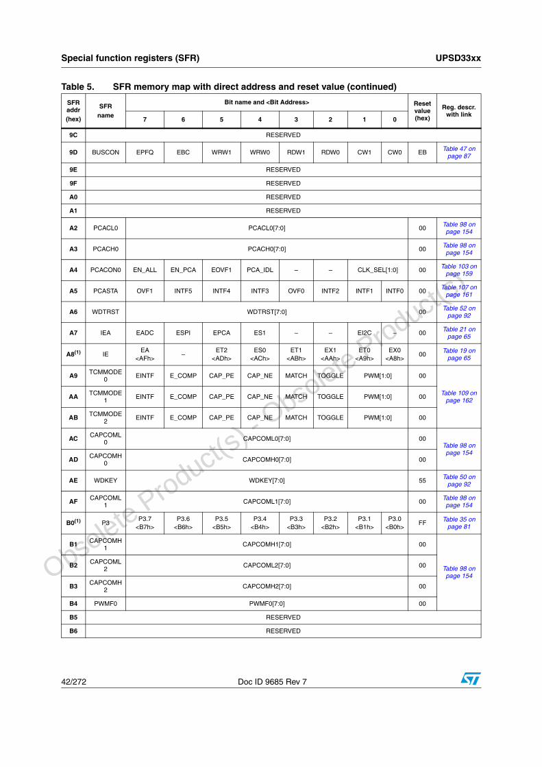
8 Special function registers (SFR)
A group of registers designated as Special Function register (SFR) is shown in Table 5 on page 41. SFRs control the operating modes of the MCU core and also control the peripheral interfaces and I/O pins on the MCU module. The SFRs can be accessed only by using the Direct Addressing method within the address range from 80h to FFh of internal 8032 SRAM. Sixteen addresses in SFR address space are both byte- and bit-addressable. The bit-addressable SFRs are noted in Table 5.
86 of a possible 128 SFR addresses are occupied. The remaining unoccupied SFR addresses (designated as “RESERVED” in Table 5) should not be written. Reading unoccupied locations will return an undefined value.
Note: There is a separate set of control registers for the PSD module, designated as csiop, and they are described in the Section 27: PSD module on page 164. The I/O pins, PLD, and other functions on the PSD module are NOT controlled by SFRs.
FC CCON3 – – – PCA1CE PCA1PS[3:0] 10 Table 101 on page 155
FD RESERVED
Table 5. SFR memory map with direct address and reset value (continued)
SFR addr(hex)
SFRname
Bit name and <Bit Address> Reset value (hex)
Reg. descr. with link
7 6 5 4 3 2 1 0
Obsolete Product(
s) - O
bsolete Product(
s)
Obsolete Product(
s) - O
bsolete Product(
s)
UPSD33xx Special function registers (SFR)
Doc ID 9685 Rev 7 45/272
FE RESERVED
FF RESERVED
1. This SFR can be addressed by individual bits (Bit Address mode) or addressed by the entire byte (Direct Address mode).
Table 5. SFR memory map with direct address and reset value (continued)
SFR addr(hex)
SFRname
Bit name and <Bit Address> Reset value (hex)
Reg. descr. with link
7 6 5 4 3 2 1 0
Obsolete Product(
s) - O
bsolete Product(
s)
Obsolete Product(
s) - O
bsolete Product(
s)
8032 addressing modes UPSD33xx
46/272 Doc ID 9685 Rev 7
9 8032 addressing modes
The 8032 MCU uses 11 different addressing modes listed below:
● Register
● Direct
● Register Indirect
● Immediate
● External Direct
● External Indirect
● Indexed
● Relative
● Absolute
● Long
● Bit
9.1 Register addressingThis mode uses the contents of one of the registers R0 - R7 (selected by the last three bits in the instruction opcode) as the operand source or destination. This mode is very efficient since an additional instruction byte is not needed to identify the operand. For example:
9.2 Direct addressingThis mode uses an 8-bit address, which is contained in the second byte of the instruction, to directly address an operand which resides in either 8032 DATA SRAM (internal address range 00h-07Fh) or resides in 8032 SFR (internal address range 80h-FFh). This mode is quite fast since the range limit is 256 bytes of internal 8032 SRAM. For example:
9.3 Register indirect addressingThis mode uses an 8-bit address contained in either register R0 or R1 to indirectly address an operand which resides in 8032 IDATA SRAM (internal address range 80h-FFh). Although 8032 SFR registers also occupy the same physical address range as IDATA, SFRs will not be accessed by register Indirect mode. SFRs may only be accesses using Direct address mode. For example:
MOV A, R7 ; Move contents of R7 to accumulator
MOV A, 40h ; Move contents of DATA SRAM; at location 40h into the accumulator
Obsolete Product(
s) - O
bsolete Product(
s)
Obsolete Product(
s) - O
bsolete Product(
s)
UPSD33xx 8032 addressing modes
Doc ID 9685 Rev 7 47/272
9.4 Immediate addressingThis mode uses 8-bits of data (a constant) contained in the second byte of the instruction, and stores it into the memory location or register indicated by the first byte of the instruction. Thus, the data is immediately available within the instruction. This mode is commonly used to initialize registers and SFRs or to perform mask operations.
There is also a 16-bit version of this mode for loading the DPTR register. In this case, the two bytes following the instruction byte contain the 16-bit value. For example:
9.5 External direct addressingThis mode will access external memory (XDATA) by using the 16-bit address stored in the DPTR register. There are only two instructions using this mode and both use the accumulator to either receive a byte from external memory addressed by DPTR or to send a byte from the accumulator to the address in DPTR. The UPSD33xx has a special feature to alternate the contents (source and destination) of DPTR rapidly to implement very efficient memory-to-memory transfers. For example:
Note: See details in Section 11: Dual data pointers on page 56.
9.6 External indirect addressingThis mode will access external memory (XDATA) by using the 8-bit address stored in either register R0 or R1. This is the fastest way to access XDATA (least bus cycles), but because only 8-bits are available for address, this mode limits XDATA to a size of only 256 bytes (the traditional Port 2 of the 8032 MCU is not available in the UPSD33xx, so it is not possible to write the upper address byte).
This mode is not supported by UPSD33xx.
For example:
MOV A, @R0 ; Move into the accumulator the
; contents of IDATA SRAM that is
; pointed to by the address ; contained in R0.
MOV A, 40# ; Move the constant, 40h, into
; the accumulator
MOV DPTR, 1234# ; Move the constant, 1234h, into
; DPTR
MOVX A, @DPTR ; Move contents of accumulator to; XDATA at address contained in
; DPTR
MOVX @DPTR, A ; Move XDATA to accumulator
Obsolete Product(
s) - O
bsolete Product(
s)
Obsolete Product(
s) - O
bsolete Product(
s)
8032 addressing modes UPSD33xx
48/272 Doc ID 9685 Rev 7
9.7 Indexed addressingThis mode is used for the MOVC instruction which allows the 8032 to read a constant from program memory (not data memory). MOVC is often used to read look-up tables that are embedded in program memory. The final address produced by this mode is the result of adding either the 16-bit PC or DPTR value to the contents of the accumulator. The value in the accumulator is referred to as an index. The data fetched from the final location in program memory is stored into the accumulator, overwriting the index value that was previously stored there. For example:
9.8 Relative addressingThis mode will add the two’s-compliment number stored in the second byte of the instruction to the program counter for short jumps within +128 or –127 addresses relative to the program counter. This is commonly used for looping and is very efficient since no additional bus cycle is needed to fetch the jump destination address. For example:
9.9 Absolute addressingThis mode will append the 5 high-order bits of the address of the next instruction to the 11 low-order bits of an ACALL or AJUMP instruction to produce a 16-bit jump address. The jump will be within the same 2 Kbyte page of program memory as the first byte of the following instruction. For example:
MOVX @R0,A ; Move into the accumulator the
; XDATA that is pointed to by
; the address contained in R0.
MOVC A, @A+DPTR ; Move code byte relative to
; DPTR into accumulator
MOVC A, @A+PC ; Move code byte relative to PC; into accumulator
SJMP 34h ; Jump 34h bytes ahead (in program
; memory) of the address at which; the SJMP instruction is stored. If
; SJMP is at 1000h, program
; execution jumps to 1034h.
AJMP 0500h ; If next instruction is located at
; address 4000h, the resulting jump
; will be made to 4500h.
Obsolete Product(
s) - O
bsolete Product(
s)
Obsolete Product(
s) - O
bsolete Product(
s)
UPSD33xx 8032 addressing modes
Doc ID 9685 Rev 7 49/272
9.10 Long addressingThis mode will use the 16-bits contained in the two bytes following the instruction byte as a jump destination address for LCALL and LJMP instructions. For example:
9.11 Bit addressingThis mode allows setting or clearing an individual bit without disturbing the other bits within an 8-bit value of internal SRAM. Bit Addressing is only available for certain locations in 8032 DATA and SFR memory. Valid locations are DATA addresses 20h - 2Fh and for SFR addresses whose base address ends with 0h or 8h. (Example: The SFR, IE, has a base address of A8h, so each of the eight bits in IE can be addressed individually at address A8h, A9h, ...up to AFh.) For example:
LJMP 0500h ; Unconditionally jump to address
; 0500h in program memory
SETB AFh ; Set the individual EA bit (Enable All
; Interrupts) inside the SFR register,; IE.
Obsolete Product(
s) - O
bsolete Product(
s)
Obsolete Product(
s) - O
bsolete Product(
s)
UPSD33xx instruction set summary UPSD33xx
50/272 Doc ID 9685 Rev 7
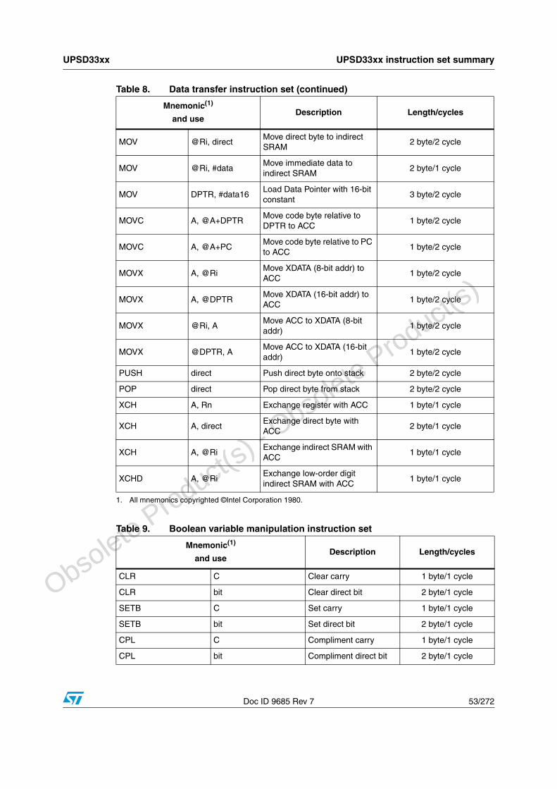
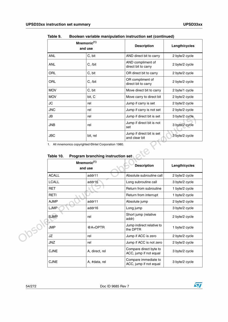
10 UPSD33xx instruction set summary
Table 6, Table 7, Table 8, Table 9, Table 10, and Table 11 list all of the instructions supported by the UPSD33xx, including the number of bytes and number of machine cycles required to implement each instruction. This is the standard 8051 instruction set.
The meaning of “machine cycles” is how many 8032 MCU core machine cycles are required to execute the instruction. The “native” duration of all machine cycles is set by the memory wait state settings in the SFR, BUSCON, and the MCU clock divider selections in the SFR, CCON0 (i.e. a machine cycle is typically set to 4 MCU clocks for a 5 V UPSD33xx). However, an individual machine cycle may grow in duration when either of two things happen:
1. Astall is imposed while loading the 8032 Pre-Fetch Queue (PFQ); or
2. The occurrence of a cache miss in the Branch Cache (BC) during a branch in program execution flow.
See Section 5: 8032 MCU core performance enhancements on page 32 or more details.
But generally speaking, during typical program execution, the PFQ is not empty and the BC has no misses, producing very good performance without extending the duration of any machine cycles.
The UPSD33xx programmers guide describes each instruction operation in detail.
Table 6. Arithmetic instruction set
Mnemonic(1)
and useDescription Length/cycles
ADD A, Rn Add register to ACC 1 byte/1 cycle
ADD A, Direct Add direct byte to ACC 2 byte/1 cycle
ADD A, @Ri Add indirect SRAM to ACC 1 byte/1 cycle
ADD A, #data Add immediate data to ACC 2 byte/1 cycle
ADDC A, Rn Add register to ACC with carry 1 byte/1 cycle
ADDC A, directAdd direct byte to ACC with carry
2 byte/1 cycle
ADDC A, @RiAdd indirect SRAM to ACC with carry
1 byte/1 cycle
ADDC A, #dataAdd immediate data to ACC with carry
2 byte/1 cycle
SUBB A, RnSubtract register from ACC with borrow
1 byte/1 cycle
SUBB A, directSubtract direct byte from ACC with borrow
2 byte/1 cycle
SUBB A, @RiSubtract indirect SRAM from ACC with borrow
1 byte/1 cycle
SUBB A, #dataSubtract immediate data from ACC with borrow
Rn Register R0 - R7 of the currently selected register bank.
direct8-bit address for internal 8032 DATA SRAM (locations 00h - 7Fh) or SFR registers (locations 80h - FFh).
@Ri8-bit internal 8032 SRAM (locations 00h - FFh) addressed indirectly through contents of R0 or R1.
#data 8-bit constant included within the instruction.
#data16 16-bit constant included within the instruction.
addr16 16-bit destination address used by LCALL and LJMP.
addr11 11-bit destination address used by ACALL and AJMP.
rel Signed (two-s compliment) 8-bit offset byte.
bitDirect addressed bit in internal 8032 DATA SRAM (locations 20h to 2Fh) or in SFR registers (88h, 90h, 98h, A8h, B0, B8h, C0h, C8h, D0h, D8h, E0h, F0h).
Table 10. Program branching instruction set (continued)
Mnemonic(1)
and useDescription Length/cycles
Obsolete Product(
s) - O
bsolete Product(
s)
Obsolete Product(
s) - O
bsolete Product(
s)
Dual data pointers UPSD33xx
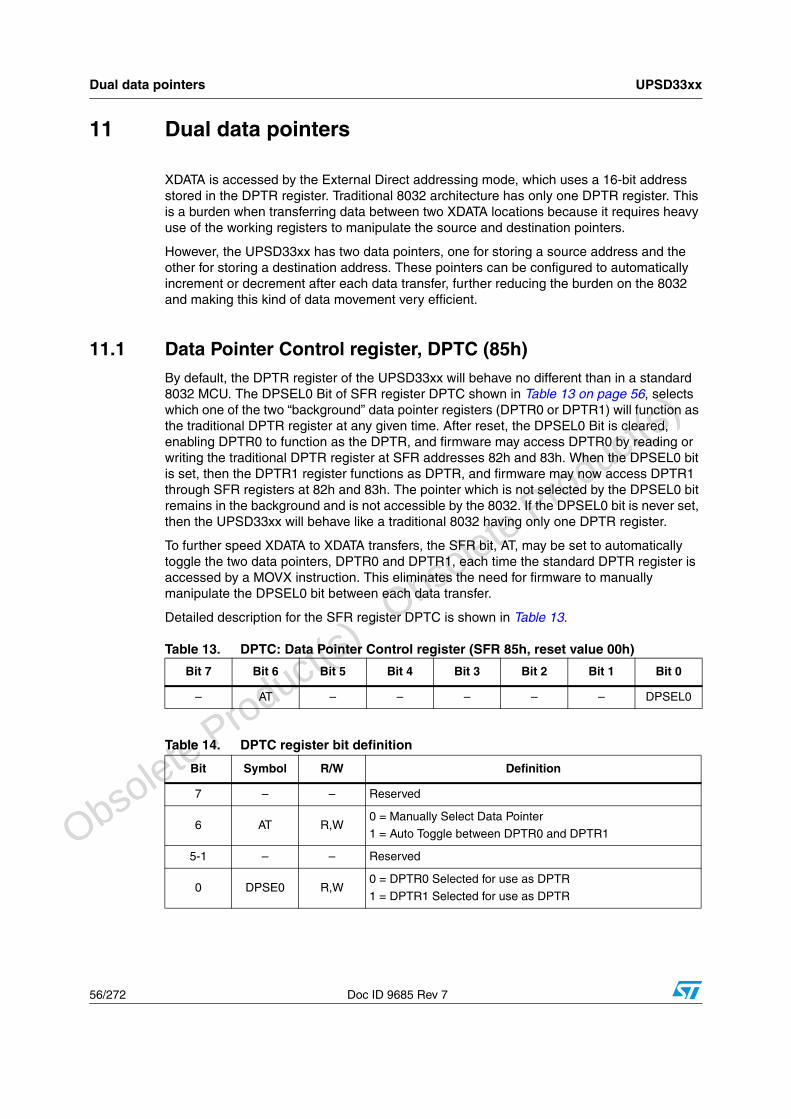
56/272 Doc ID 9685 Rev 7
11 Dual data pointers
XDATA is accessed by the External Direct addressing mode, which uses a 16-bit address stored in the DPTR register. Traditional 8032 architecture has only one DPTR register. This is a burden when transferring data between two XDATA locations because it requires heavy use of the working registers to manipulate the source and destination pointers.
However, the UPSD33xx has two data pointers, one for storing a source address and the other for storing a destination address. These pointers can be configured to automatically increment or decrement after each data transfer, further reducing the burden on the 8032 and making this kind of data movement very efficient.
11.1 Data Pointer Control register, DPTC (85h)By default, the DPTR register of the UPSD33xx will behave no different than in a standard 8032 MCU. The DPSEL0 Bit of SFR register DPTC shown in Table 13 on page 56, selects which one of the two “background” data pointer registers (DPTR0 or DPTR1) will function as the traditional DPTR register at any given time. After reset, the DPSEL0 Bit is cleared, enabling DPTR0 to function as the DPTR, and firmware may access DPTR0 by reading or writing the traditional DPTR register at SFR addresses 82h and 83h. When the DPSEL0 bit is set, then the DPTR1 register functions as DPTR, and firmware may now access DPTR1 through SFR registers at 82h and 83h. The pointer which is not selected by the DPSEL0 bit remains in the background and is not accessible by the 8032. If the DPSEL0 bit is never set, then the UPSD33xx will behave like a traditional 8032 having only one DPTR register.
To further speed XDATA to XDATA transfers, the SFR bit, AT, may be set to automatically toggle the two data pointers, DPTR0 and DPTR1, each time the standard DPTR register is accessed by a MOVX instruction. This eliminates the need for firmware to manually manipulate the DPSEL0 bit between each data transfer.
Detailed description for the SFR register DPTC is shown in Table 13.
Table 13. DPTC: Data Pointer Control register (SFR 85h, reset value 00h)
Bit 7 Bit 6 Bit 5 Bit 4 Bit 3 Bit 2 Bit 1 Bit 0
– AT – – – – – DPSEL0
Table 14. DPTC register bit definition
Bit Symbol R/W Definition
7 – – Reserved
6 AT R,W0 = Manually Select Data Pointer
1 = Auto Toggle between DPTR0 and DPTR1
5-1 – – Reserved
0 DPSE0 R,W0 = DPTR0 Selected for use as DPTR
1 = DPTR1 Selected for use as DPTR
Obsolete Product(
s) - O
bsolete Product(
s)
Obsolete Product(
s) - O
bsolete Product(
s)
UPSD33xx Dual data pointers
Doc ID 9685 Rev 7 57/272
11.2 Data Pointer Mode register, DPTM (86h)The two “background” data pointers, DPTR0 and DPTR1, can be configured to automatically increment, decrement, or stay the same after a MOVX instruction accesses the DPTR register. Only the currently selected pointer will be affected by the increment or decrement. This feature is controlled by the DPTM register defined in Table 15.
The automatic increment or decrement function is effective only for the MOVX instruction, and not MOVC or any other instruction that uses the DTPR register.
11.2.1 Firmware example
The 8051 assembly code illustrated in Table 17 shows how to transfer a block of data bytes from one XDATA address region to another XDATA address region. Auto-address incrementing and auto-pointer toggling will be used.
Table 15. DPTM: Data Pointer Mode register (SFR 86h, reset value 00h)
Bit 7 Bit 6 Bit 5 Bit 4 Bit 3 Bit 2 Bit 1 Bit 0
– – – – MD11 MD10 MD01 MD00
Table 16. DPTM register bit definition
Bit Symbol R/W Definition
7-4 – – Reserved
3-2 MD[11:10] R,W
DPTR1 Mode Bits00: DPTR1 No Change
01: Reserved
10: Auto Increment11: Auto Decrement
1-0 MD[01:00] R,W
DPTR0 Mode Bits00: DPTR0 No Change
01: Reserved
10: Auto Increment11: Auto Decrement
Obsolete Product(
s) - O
bsolete Product(
s)
Obsolete Product(
s) - O
bsolete Product(
s)
Dual data pointers UPSD33xx
58/272 Doc ID 9685 Rev 7
Table 17. 8051 assembly code exampleMOV R7, #COUNT ; initialize size of data block to transfer
MOV DPTR, #SOURCE_ADDR
; load XDATA source address base into DPTR0
MOV 85h, #01h ; load DPTC to access DPTR1 pointer
MOV DPTR, #DEST_ADDR ; load XDATA destination address base into DPTR1
MOV 85h, #40h ; load DPTC to access DPTR0 pointer and auto toggle
MOV 86h, #0Ah ; load DPTM to auto-increment both pointers
LOOP: MOVX(1)
1. The code loop where the data transfer takes place is only 3 lines of code.
A, @DPTR ; load XDATA byte from source into ACC.
; after load completes, DPTR0 increments and DPTR
; switches DPTR1
MOVX(1) @DPTR, A ; store XDATA byte from ACC to destination.; after store completes, DPTR1 increments and DPTR; switches to DPTR0
DJNZ(1) R7, LOOP ; continue until done
MOV 86h, #00 ; disable auto-increment
MOV 85h, #00 ; disable auto-toggle, now back to single DPTR mode
Obsolete Product(
s) - O
bsolete Product(
s)
Obsolete Product(
s) - O
bsolete Product(
s)
UPSD33xx Debug unit
Doc ID 9685 Rev 7 59/272
12 Debug unit
The 8032 MCU module supports run-time debugging through the JTAG interface. This same JTAG interface is also used for in-system programming (ISP) and the physical connections are described in the PSD module section, Section 27.5.1: JTAG ISP and JTAG debug on page 233.
Debugging with a serial interface such as JTAG is a non-intrusive way to gain access to the internal state of the 8032 MCU core and various memories. A traditional external hardware emulator cannot be completely effective on the UPSD33xx because of the Pre-Fetch Queue and Branch Cache. The nature of the PFQ and BC hide the visibility of actual program flow through traditional external bus connections, thus requiring on-chip serial debugging instead.
Debugging is supported by Windows PC based software tools used for 8051 code development from 3rd party vendors listed at www.st.com/mcu. Debug capabilities include:
● Halt or start MCU execution
● Reset the MCU
● Single step
● 3 match breakpoints
● 1 range breakpoint (inside or outside range)
● Program tracing
● Read or modify MCU core registers, DATA, IDATA, SFR, XDATA, and code
● External Debug Event pin, input or output
Some key points regarding use of the JTAG debugger.
● The JTAG debugger can access MCU registers, data memory, and code memory while the MCU is executing at full speed by cycle-stealing. This means “watch windows” may be displayed and periodically updated on the PC during full speed operation. registers and data content may also be modified during full speed operation.
● There is no on-chip storage for Program Trace data, but instead this data is scanned from the UPSD33xx through the JTAG channel at run-time to the PC host for processing. As such, full speed program tracing is possible only when the 8032 MCU is operating below approximately one MIPS of performance. Above one MIPS, the program will not run real-time while tracing. One MIPS performance is determined by the combination of choice for MCU clock frequency, and the bit settings in SFR registers BUSCON and CCON0.
● Breakpoints can optionally halt the MCU, and/or assert the external Debug Event pin.
● Breakpoint definitions may be qualified with read or write operations, and may also be qualified with an address of code, SFR, DATA, IDATA, or XDATA memories.
● Three breakpoints will compare an address, but the fourth breakpoint can compare an address and also data content. Additionally, the fourth breakpoint can be logically combined (AND/OR) with any of the other three breakpoints.
● The Debug Event pin can be configured by the PC host to generate an output pulse for external triggering when a break condition is met. The pin can also be configured as an event input to the breakpoint logic, causing a break on the falling-edge of an external
Obsolete Product(
s) - O
bsolete Product(
s)
Obsolete Product(
s) - O
bsolete Product(
s)
Debug unit UPSD33xx
60/272 Doc ID 9685 Rev 7
event signal. If not used, the Debug Event pin should be pulled up to VCC as described in Section 27.5.8: Debugging the 8032 MCU module on page 240.
● The duration of a pulse, generated when the Event pin configured as an output, is one MCU clock cycle. This is an active-low signal, so the first edge when an event occurs is high-to-low.
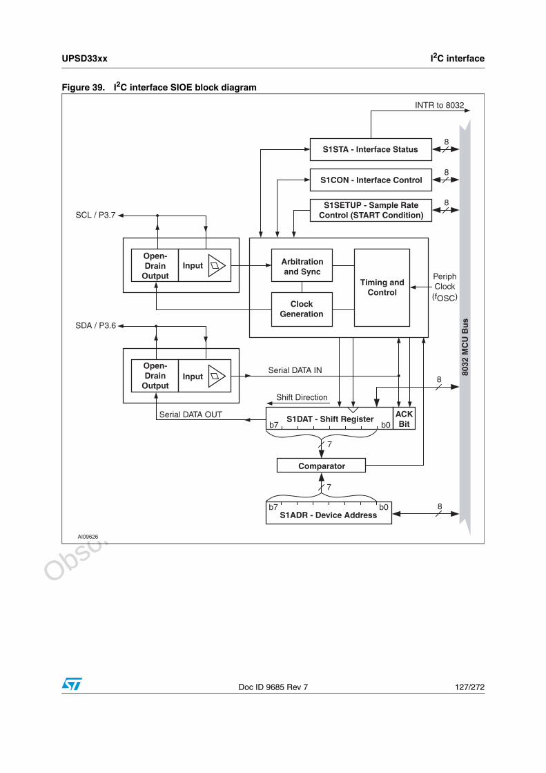
● The clock to the Watchdog timer, ADC, and I2C interface are not stopped by a breakpoint halt.
● The Watchdog timer should be disabled while debugging with JTAG, else a reset will be generated upon a watchdog timeout.
Obsolete Product(
s) - O
bsolete Product(
s)
Obsolete Product(
s) - O
bsolete Product(
s)
UPSD33xx Interrupt system
Doc ID 9685 Rev 7 61/272
13 Interrupt system
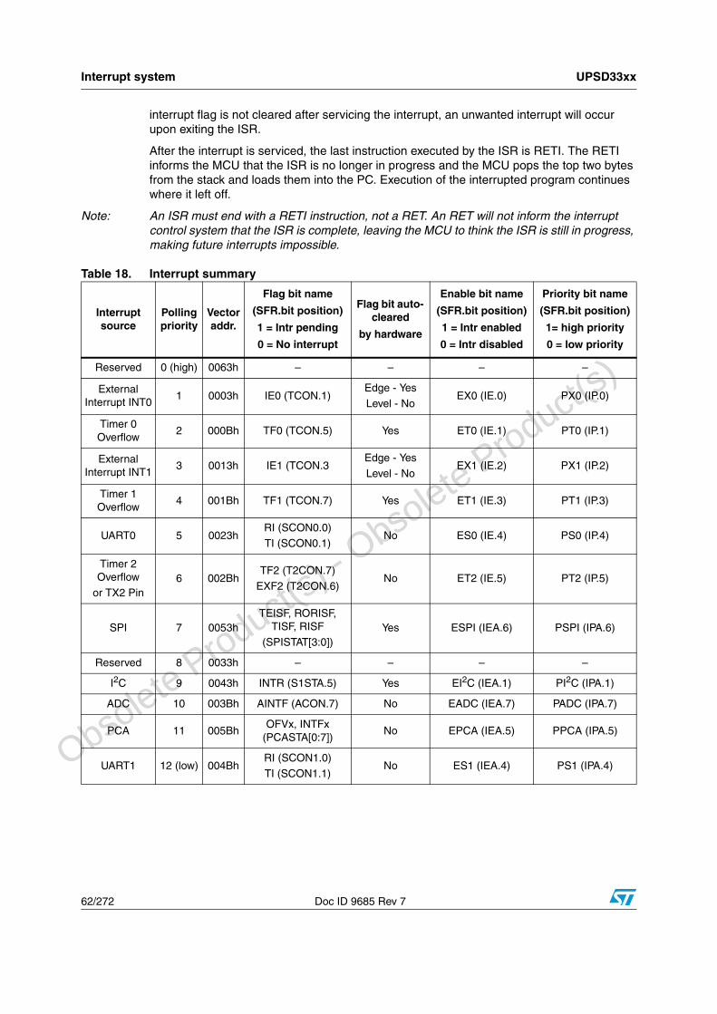
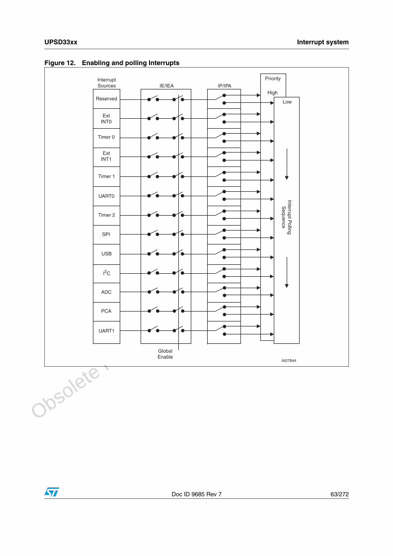
The UPSD33xx has an 11-source, two priority level interrupt structure summarized in Table 18.
Firmware may assign each interrupt source either high or low priority by writing to bits in the SFRs named, IP and IPA, shown in Table 18. An interrupt will be serviced as long as an interrupt of equal or higher priority is not already being serviced. If an interrupt of equal or higher priority is being serviced, the new interrupt will wait until it is finished before being serviced. If a lower priority interrupt is being serviced, it will be stopped and the new interrupt is serviced. When the new interrupt is finished, the lower priority interrupt that was stopped will be completed. If new interrupt requests are of the same priority level and are received simultaneously, an internal polling sequence determines which request is selected for service. Thus, within each of the two priority levels, there is a second priority structure determined by the polling sequence.
Firmware may individually enable or disable interrupt sources by writing to bits in the SFRs named, IE and IEA, shown in Table 18 on page 62. The SFR named IE contains a global disable bit (EA), which can be cleared to disable all 11 interrupts at once, as shown in Table 19 on page 65. Figure 12 on page 63 illustrates the interrupt priority, polling, and enabling process.
Each interrupt source has at least one interrupt flag that indicates whether or not an interrupt is pending. These flags reside in bits of various SFRs shown in Table 18 on page 62.
All of the interrupt flags are latched into the interrupt control system at the beginning of each MCU machine cycle, and they are polled at the beginning of the following machine cycle. If polling determines one of the flags was set, the interrupt control system automatically generates an LCALL to the user’s Interrupt Service Routine (ISR) firmware stored in program memory at the appropriate vector address.
The specific vector address for each of the interrupt sources are listed in Table 18 on page 62. However, this LCALL jump may be blocked by any of the following conditions:
● An interrupt of equal or higher priority is already in progress
● The current machine cycle is not the final cycle in the execution of the instruction in progress
● The current instruction involves a write to any of the SFRs: IE, IEA, IP, or IPA
● The current instruction is an RETI
Note: Interrupt flags are polled based on a sample taken in the previous MCU machine cycle. If an interrupt flag is active in one cycle but is denied serviced due to the conditions above, and then later it is not active when the conditions above are finally satisfied, the previously denied interrupt will not be serviced. This means that active interrupts are not remembered. Every poling cycle is new.
Assuming all of the listed conditions are satisfied, the MCU executes the hardware generated LCALL to the appropriate ISR. This LCALL pushes the contents of the PC onto the stack (but it does not save the PSW) and loads the PC with the appropriate interrupt vector address. Program execution then jumps to the ISR at the vector address.
Execution precedes in the ISR. It may be necessary for the ISR firmware to clear the pending interrupt flag for some interrupt sources, because not all interrupt flags are automatically cleared by hardware when the ISR is called, as shown in Table 18. If an
Obsolete Product(
s) - O
bsolete Product(
s)
Obsolete Product(
s) - O
bsolete Product(
s)
Interrupt system UPSD33xx
62/272 Doc ID 9685 Rev 7
interrupt flag is not cleared after servicing the interrupt, an unwanted interrupt will occur upon exiting the ISR.
After the interrupt is serviced, the last instruction executed by the ISR is RETI. The RETI informs the MCU that the ISR is no longer in progress and the MCU pops the top two bytes from the stack and loads them into the PC. Execution of the interrupted program continues where it left off.
Note: An ISR must end with a RETI instruction, not a RET. An RET will not inform the interrupt control system that the ISR is complete, leaving the MCU to think the ISR is still in progress, making future interrupts impossible.
ADC 10 003Bh AINTF (ACON.7) No EADC (IEA.7) PADC (IPA.7)
PCA 11 005BhOFVx, INTFx
(PCASTA[0:7])No EPCA (IEA.5) PPCA (IPA.5)
UART1 12 (low) 004BhRI (SCON1.0)
TI (SCON1.1)No ES1 (IEA.4) PS1 (IPA.4)
Obsolete Product(
s) - O
bsolete Product(
s)
Obsolete Product(
s) - O
bsolete Product(
s)
UPSD33xx Interrupt system
Doc ID 9685 Rev 7 63/272
Figure 12. Enabling and polling Interrupts
Reserved
ExtINT0
ExtINT1
Timer 0
UART0
Timer 1
SPI
USB
Timer 2
High
LowInterrupt P
ollingS
equence
InterruptSources IE/IEA IP/IPA
Priority
GlobalEnable
ADC
PCA
I2C
UART1
AI07844
Obsolete Product(
s) - O
bsolete Product(
s)
Obsolete Product(
s) - O
bsolete Product(
s)
Interrupt system UPSD33xx
64/272 Doc ID 9685 Rev 7
13.1 Individual interrupt sources
13.1.1 External interrupts Int0 and Int1
External interrupt inputs on pins EXTINT0 and EXTINT1 (pins 3.2 and 3.3) are either edge-triggered or level-triggered, depending on bits IT0 and IT1 in the SFR named TCON.
When an external interrupt is generated from an edge-triggered (falling-edge) source, the appropriate flag bit (IE0 or IE1) is automatically cleared by hardware upon entering the ISR.
When an external interrupt is generated from a level-triggered (low-level) source, the appropriate flag bit (IE0 or IE1) is NOT automatically cleared by hardware.
13.1.2 Timer 0 and 1 overflow interrupt
Timer 0 and Timer 1 interrupts are generated by the flag bits TF0 and TF1 when there is an overflow condition in the respective Timer/Counter register (except for Timer 0 in mode 3).
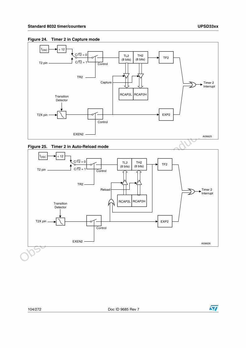
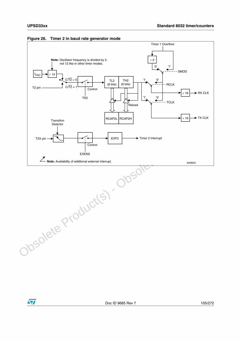
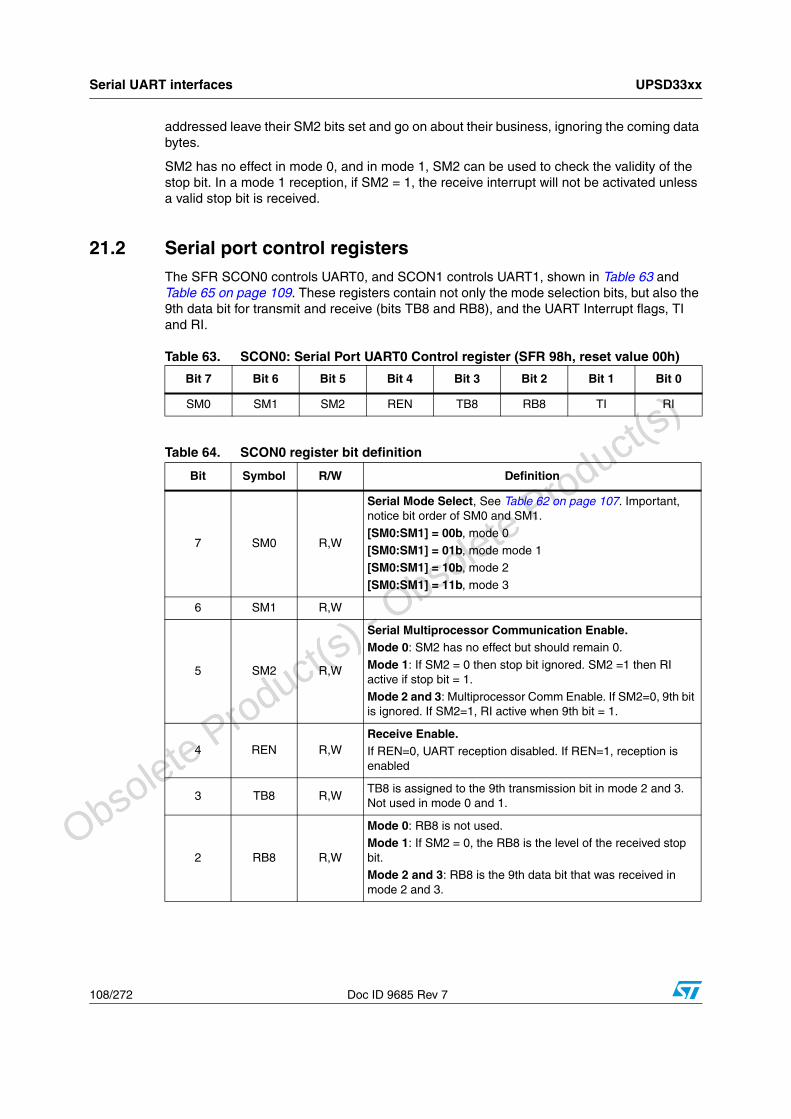
13.1.3 Timer 2 overflow interrupt
This interrupt is generated to the MCU by a logical OR of flag bits, TF2 and EXE2. The ISR must read the flag bits to determine the cause of the interrupt.
● TF2 is set by an overflow of Timer 2.
● EXE2 is generated by the falling edge of a signal on the external pin, T2X (pin P1.1).
13.1.4 UART0 and UART1 interrupt
Each of the UARTs have identical interrupt structure. For each UART, a single interrupt is generated to the MCU by the logical OR of the flag bits, RI (byte received) and TI (byte transmitted).
The ISR must read flag bits in the SFR named SCON0 for UART0, or SCON1 for UART1 to determine the cause of the interrupt.
13.1.5 SPI interrupt
The SPI interrupt has four interrupt sources, which are logically ORed together when interrupting the MCU. The ISR must read the flag bits to determine the cause of the interrupt.
A flag bit is set for: end of data transmit (TEISF); data receive overrun (RORISF); transmit buffer empty (TISF); or receive buffer full (RISF).
13.1.6 I2C interrupt
The flag bit INTR is set by a variety of conditions occurring on the I2C interface: received own slave address (ADDR flag); received general call address (GC flag); received STOP condition (STOP flag); or successful transmission or reception of a data byte.The ISR must read the flag bits to determine the cause of the interrupt.
13.1.7 ADC interrupt
The flag bit AINTF is set when an A-to-D conversion has completed.
Obsolete Product(
s) - O
bsolete Product(
s)
Obsolete Product(
s) - O
bsolete Product(
s)
UPSD33xx Interrupt system
Doc ID 9685 Rev 7 65/272
13.1.8 PCA interrupt
The PCA has eight interrupt sources, which are logically ORed together when interrupting the MCU.The ISR must read the flag bits to determine the cause of the interrupt.
● Each of the six TCMs can generate a "match or capture" interrupt on flag bits OFV5..0 respectively.
● Each of the two 16-bit counters can generate an overflow interrupt on flag bits INTF1 and INTF0 respectively.
Table 19, Table 18, Table 19, and Table 21 have detailed bit definitions of the interrupt system SFRs.
Global disable bit 0 = All interrupts are disabled.
1 = Each interrupt source can be individually enabled or disabled by setting or clearing its enable bit.
6 – R,WDo not modify this bit. It is used by the JTAG debugger for instruction tracing. Always read the bit and write back the same bit value when writing this SFR.
Internal system clocks generated by the clock generation unit are derived from the signal, XTAL1, shown in Figure 13 on page 69. XTAL1 has a frequency fOSC, which comes directly from the external crystal or oscillator device. The SFR named CCON0 (Table 27 on page 69) controls the clock generation unit.
There are two clock signals produced by the clock generation unit:
● MCU_CLK
● PERIPH_CLK
14.1 MCU_CLKThis clock drives the 8032 MCU core and the watchdog timer (WDT). The frequency of MCU_CLK is equal to fOSC by default, but it can be divided by as much as 2048, shown in Figure 13 on page 69. The bits CPUPS[2:0] select one of eight different divisors, ranging from 2 to 2048. The new frequency is available immediately after the CPUPS[2:0] bits are written. The final frequency of MCU_CLK is fMCU.
MCU_CLK is blocked by either bit, PD or IDL, in the SFR named PCON during MCU Power-down mode or Idle mode respectively.
MCU_CLK clock can be further divided as required for use in the WDT. See details of the WDT in Section 19: Supervisory functions on page 89.
14.2 PERIPH_CLKThis clock drives all the UPSD33xx peripherals except the WDT. The Frequency of PERIPH_CLK is always fOSC. Each of the peripherals can independently divide PERIPH_CLK to scale it appropriately for use.
PERIPH_CLK runs at all times except when blocked by the PD bit in the SFR named PCON during MCU Power-down mode.
14.2.1 JTAG interface clock
The JTAG interface for ISP and for debugging uses the externally supplied JTAG clock, coming in on pin TCK. This means the JTAG ISP interface is always available, and the JTAG debug interface is available when enabled, even during MCU Idle mode and Power-down mode.
However, since the MCU participates in the JTAG debug process, and MCU_CLK is halted during Idle and Power-down modes, the majority of debug functions are not available during these low power modes. But the JTAG debug interface is capable of executing a reset command while in these low power modes, which will exit back to normal operating mode where all debug commands are available again.
The CCON0 SFR contains a bit, DBGCE, which enables the breakpoint comparators inside the JTAG debug Unit when set. DBGCE is set by default after reset, and firmware may clear this bit at run-time. Disabling these comparators will reduce current consumption on the MCU module, and it’s recommended to do so if the debug unit will not be used (such as in the production version of an end-product).
Obsolete Product(
s) - O
bsolete Product(
s)
Obsolete Product(
s) - O
bsolete Product(
s)
UPSD33xx MCU clock generation
Doc ID 9685 Rev 7 69/272
Figure 13. Clock generation logic
Table 28. CCON0 register bit definition
XTAL1 /2
XTAL1 /4
XTAL1 /2048
Q
Q
Q
MUX
XTAL1 (default)
XTAL1 /8
XTAL1 /16Q
QXTAL1 /32
XTAL1 /1024Q
Q
0
1
2
3
4
5
6
7
XTAL1(fOSC)
PCON[1]: PD,Power-Down Mode
CCON[2:0]Clock Pre-Scaler Select
PCON[0]: IDL,Idle Mode
Clock Divider
MCU_CLK (fMCU)
(to: 8032, WDT)
PERIPH_CLK (fOSC)
(to: TIMER0/1/2, UART0/1, PCA0/1, SPI, I2C, ADC)
3
AI09197b
Table 27. CCON0: Clock Control register (SFR F9h, reset value 10h)
Bit 7 Bit 6 Bit 5 Bit 4 Bit 3 Bit 2 Bit 1 Bit 0
– – – DBGCE CPUAR CPUPS[2:0]
Bit Symbol R/W Definition
7 – – Reserved
6 – – Reserved
5 – – Reserved
4 DBGCE R,WDebug Unit Breakpoint Comparator Enable0 = JTAG debug unit comparators are disabled
1 = JTAG debug unit comparators are enabled (Default condition after reset)
3 CPUAR R,W
Automatic MCU Clock Recovery0 = There is no change of CPUPS[2:0] when an interrupt occurs.
1 = Contents of CPUPS[2:0] automatically become 000b whenever any interrupt occurs.
2:0 CPUPS R,W
MCUCLK Pre-Scaler000b: fMCU = fOSC (Default after reset)
001b: fMCU = fOSC/2
010b: fMCU = fOSC/4011b: fMCU = fOSC/8
100b: fMCU = fOSC/16
101b: fMCU = fOSC/32110b: fMCU = fOSC/1024
111b: fMCU = fOSC/2048
Obsolete Product(
s) - O
bsolete Product(
s)
Obsolete Product(
s) - O
bsolete Product(
s)
Power saving modes UPSD33xx
70/272 Doc ID 9685 Rev 7
15 Power saving modes
The UPSD33xx is a combination of two die, or modules, each module having it’s own current consumption characteristics. This section describes reduced power modes for the MCU module. See Section 27.1.16: Power management on page 170 for reduced power modes of the PSD module. Total current consumption for the combined modules is determined in the DC specifications at the end of this document.
The MCU module has three software-selectable modes of reduced power operation.
● Idle mode
● Power-down mode
● Reduced Frequency mode
15.1 Idle modeIdle mode will halt the 8032 MCU core while leaving the MCU peripherals active (Idle mode blocks MCU_CLK only). For lowest current consumption in this mode, it is recommended to disable all unused peripherals, before entering Idle mode (such as the ADC and the debug unit breakpoint comparators). The following functions remain fully active during Idle mode (except if disabled by SFR settings).
● External Interrupts INT0 and INT1
● Timer 0, Timer 1 and Timer 2
● Supervisor reset from: LVD, JTAG debug, external RESET_IN_, but not the WTD
● ADC
● I2C Interface
● UART0 and UART1 Interfaces
● SPI Interface
● Programmable Counter Array
An interrupt generated by any of these peripherals, or a reset generated from the supervisor, will cause Idle mode to exit and the 8032 MCU will resume normal operation.
The output state on I/O pins of MCU ports 1, 3, and 4 remain unchanged during Idle mode.
To enter Idle mode, the 8032 MCU executes an instruction to set the IDL bit in the SFR named PCON, shown in Table 31 on page 72. This is the last instruction executed in normal operating mode before Idle mode is activated. Once in Idle mode, the MCU status is entirely preserved, and there are no changes to: SP, PSW, PC, ACC, SFRs, DATA, IDATA, or XDATA.
The following are factors related to Idle mode exit:
● Activation of any enabled interrupt will cause the IDL bit to be cleared by hardware, terminating Idle mode. The interrupt is serviced, and following the Return from Interrupt instruction (RETI), the next instruction to be executed will be the one which follows the instruction that set the IDL bit in the PCON SFR.
● After a reset from the supervisor, the IDL bit is cleared, Idle mode is terminated, and the MCU restarts after three MCU machine cycles.
Obsolete Product(
s) - O
bsolete Product(
s)
Obsolete Product(
s) - O
bsolete Product(
s)
UPSD33xx Power saving modes
Doc ID 9685 Rev 7 71/272
15.2 Power-down modePower-down mode will halt the 8032 core and all MCU peripherals (Power-down mode blocks MCU_CLK and PERIPH_CLK). This is the lowest power state for the MCU module. When the PSD module is also placed in Power-down mode, the lowest total current consumption for the combined die is achieved for the UPSD33xx. See Section 27.1.16: Power management on page 170 in the PSD module section for details on how to also place the PSD module in Power-down mode. The sequence of 8032 instructions is important when placing both modules into Power-down mode.
The instruction that sets the PD Bit in the SFR named PCON (Table 31 on page 72) is the last instruction executed prior to the MCU module going into Power-down mode. Once in Power-down mode, the on-chip oscillator circuitry and all clocks are stopped. The SFRs, DATA, IDATA, and XDATA are preserved.
Power-down mode is terminated only by a reset from the supervisor, originating from the RESET_IN_ pin, the low-Voltage Detect circuit (LVD), or a JTAG debug reset command. Since the clock to the WTD is not active during Power-down mode, it is not possible for the supervisor to generate a WDT reset.
Table 29 on page 72 summarizes the status of I/O pins and peripherals during Idle and Power-down modes on the MCU module. Table 30 on page 72 shows the state of 8032 MCU address, data, and control signals during these modes.
15.3 Reduced frequency modeThe 8032 MCU consumes less current when operating at a lower clock frequency. The MCU can reduce it’s own clock frequency at run-time by writing to three bits, CPUPS[2:0], in the SFR named CCON0 described in Table 27 on page 69. These bits effectively divide the clock frequency (fOSC) coming in from the external crystal or oscillator device. The clock division range is from 1/2 to 1/2048, and the resulting frequency is fMCU.
This MCU clock division does not affect any of the peripherals, except for the WTD. The clock driving the WTD is the same clock driving the 8032 MCU core as shown in Figure 13 on page 69.
MCU firmware may reduce the MCU clock frequency at run-time to consume less current when performing tasks that are not time critical, and then restore full clock frequency as required to perform urgent tasks.
Returning to full clock frequency is done automatically upon an MCU interrupt, if the CPUAR Bit in the SFR named CCON0 is set (the interrupt will force CPUPS[2:0] = 000). This is an excellent way to conserve power using a low frequency clock until an event occurs that requires full performance. See Table 27 on page 69 for details on CPUAR.
See the DC Specifications at the end of this document to estimate current consumption based on the MCU clock frequency.
Note: Some of the bits in the PCON SFR shown in Table 31 on page 72 are not related to power control.
Obsolete Product(
s) - O
bsolete Product(
s)
Obsolete Product(
s) - O
bsolete Product(
s)
Power saving modes UPSD33xx
72/272 Doc ID 9685 Rev 7
Table 29. MCU module port and peripheral status during reduced power modes
Table 30. State of 8032 MCU bus Signals during Power-down and Idle modes
Table 31. PCON: Power Control register (SFR 87h, reset value 00h)
ModePorts 1,
3, 4PCA SPI I2C ADC
SUPERVISOR
UART0,
UART1TIMER 0,1,2
EXT INT0, 1
IdleMaintain
DataActive Active Active Active Active(1)
1. The watchdog timer is not active during Idle mode. Other supervisor functions are active: LVD, external reset, JTAG debug reset
Baud Rate Double Bit (UART0)0 = No Doubling1 = Doubling
(See Section 21.3: UART baud rates on page 110 for details.)
6 SMOD1 R,W
Baud Rate Double Bit for 2nd UART (UART1)0 = No Doubling1 = Doubling
(See Section 21.3: UART baud rates on page 110 for details.)
5 – – Reserved
4 POR R,W
Only a power-on, and a Reset sets this bit (cold reset). Warm reset will not set this bit.'0,' Cleared to zero with firmware
'1,' Is set only by a power-on reset generated by Supervisory circuit (see Section 19.3: Power-up reset on page 90 for details).
3 RCLK1 R,WReceived Clock Flag (UART1) (See Table 58 on page 100 for flag description.)
Obsolete Product(
s) - O
bsolete Product(
s)
Obsolete Product(
s) - O
bsolete Product(
s)
UPSD33xx Power saving modes
Doc ID 9685 Rev 7 73/272
2 TCLK1 R,WTransmit Clock Flag (UART1) (See Table 58 on page 100 for flag description)
1 PD R,WActivate Power-down mode0 = Not in Power-down mode
1 = Enter Power-down mode
0 IDL R,W
Activate Idle mode0 = Not in Idle mode
1 = Enter Idle mode
Table 32. PCON register bit definition (continued)
Bit Symbol R/W Function
Obsolete Product(
s) - O
bsolete Product(
s)
Obsolete Product(
s) - O
bsolete Product(
s)
Oscillator and external components UPSD33xx
74/272 Doc ID 9685 Rev 7
16 Oscillator and external components
The oscillator circuit of UPSD33xx devices is a single stage, inverting amplifier in a Pierce oscillator configuration. The internal circuitry between pins XTAL1 and XTAL2 is basically an inverter biased to the transfer point. Either an external quartz crystal or ceramic resonator can be used as the feedback element to complete the oscillator circuit. Both are operated in parallel resonance. Ceramic resonators are lower cost, but typically have a wider frequency tolerance than quartz crystals. Alternatively, an external clock source from an oscillator or other active device may drive the UPSD33xx oscillator circuit input directly, instead of using a crystal or resonator.
The minimum frequency of the quartz crystal, ceramic resonator, or external clock source is 1 MHz if the I2C interface is not used. The minimum is 8 MHz if I2C is used. The maximum is 40 MHz in all cases. This frequency is fOSC, which can be divided internally as described in Section 14: MCU clock generation on page 68.
The pin XTAL1 is the high gain amplifier input, and XTAL2 is the output. To drive the UPSD33xx device externally from an oscillator or other active device, XTAL1 is driven and XTAL2 is left open-circuit. This external source should drive a logic low at the voltage level of 0.3 VCC or below, and logic high at 0.7 VCC or above, up to 5.5 VCC. The XTAL1 input is 5 V tolerant.
Most of the quartz crystals in the range of 25 MHz to 40 MHz operate in the third overtone frequency mode. An external LC tank circuit at the XTAL2 output of the oscillator circuit is needed to achieve the third overtone frequency, as shown in Figure 14 on page 75. Without this LC circuit, the crystal will oscillate at a fundamental frequency mode that is about 1/3 of the desired overtone frequency.
Note: In Figure 14 on page 75 crystals which are specified to operate in fundamental mode (not overtone mode) do not need the LC circuit components. Since quartz crystals and ceramic resonators have their own characteristics based on their manufacturer, it is wise to also consult the manufacturer’s recommended values for external components.
Obsolete Product(
s) - O
bsolete Product(
s)
Obsolete Product(
s) - O
bsolete Product(
s)
UPSD33xx Oscillator and external components
Doc ID 9685 Rev 7 75/272
Figure 14. Oscillator and clock connections
Crystal or ResonatorUsage
Direct Drive
XTAL1(in)
XTAL1(in)
XTAL2(out)
XTAL2(out)
C1 C2XTAL(fOSC)
L1
C3
No ConnectExternal Ocsillator orActive Clock Source
XTAL (fOSC) C1 = C2 C3 L1
Ceramic Resonator 40 - 50pF None
Crystal, fundamental mode (3-40MHz) 15-33pF None
None
None
Crystal, overtone mode (25-40MHz) 20pF 10nF 2.2µH
AI09198
Obsolete Product(
s) - O
bsolete Product(
s)
Obsolete Product(
s) - O
bsolete Product(
s)
I/O ports of MCU module UPSD33xx
76/272 Doc ID 9685 Rev 7
17 I/O ports of MCU module
The MCU module has three 8-bit I/O ports: Port 1, Port 3, and Port 4. The PSD module has four other I/O ports: Port A, B, C, and D. This section describes only the I/O ports on the MCU module.
I/O ports will function as bi-directional General Purpose I/O (GPIO), but the port pins can have alternate functions assigned at run-time by writing to specific SFRs. The default operating mode (during and after reset) for all three ports is GPIO input mode. Port pins that have no external connection will not float because each pin has an internal weak pull-up (~150 kOhms) to VCC.
I/O ports 3 and 4 are 5 V tolerant, meaning they can be driven/pulled externally up to 5.5 V without damage. The pins on Port 4 have a higher current capability than the pins on Ports 1 and 3.
Three additional MCU ports (only on 80-pin UPSD33xx devices) are dedicated to bring out the 8032 MCU address, data, and control signals to external pins. One port, named MCUA[11:8], contains four MCU address signal outputs. Another port, named MCUAD[7:0], has eight multiplexed address/data bidirectional signals. The third port has MCU bus control outputs: read, write, program fetch, and address latch. These ports are typically used to connect external parallel peripherals and memory devices, but they may NOT be used as GPIO. Notice that only four of the eight upper address signals come out to pins on the port MCUA[11:8]. If additional high-order address signals are required on external pins (MCU addresses A[15:12]), then these address signals can be brought out as needed to PLD output pins or to the Address Out mode pins on PSD module ports. See Section 27.4.39: Latched address output mode on page 214 for details.
Figure 15 on page 78 represents the flexibility of pin function routing controlled by the SFRs. Each of the 24 pins on three ports, P1, P3, and P4, may be individually routed on a pin-by-pin basis to a desired function.
17.1 MCU port operating modesMCU port pins can operate as GPIO or as alternate functions (see Figure 16 through Figure 18 on page 80).
Depending on the selected pin function, a particular pin operating mode will automatically be used:
● GPIO - quasi-bidirectional mode
● UART0, UART1 - quasi-bidirectional mode
● SPI - quasi-bidirectional mode
● I2C - open drain mode
● ADC - analog input mode
● PCA output - push-pull mode
● PCA input - input only (quasi-bidirectional)
● Timer 0,1,2 - input only (quasi-bidirectional)
Obsolete Product(
s) - O
bsolete Product(
s)
Obsolete Product(
s) - O
bsolete Product(
s)
UPSD33xx I/O ports of MCU module
Doc ID 9685 Rev 7 77/272
17.1.1 GPIO function
Ports in GPIO mode operate as quasi-bidirectional pins, consistent with standard 8051 architecture. GPIO pins are individually controlled by three SFRs:
● SFR, P1 (Table 33 on page 80)
● SFR, P3 (Table 35 on page 81)
● SFR, P4 (Table 37 on page 81)
These SFRs can be accessed using the Bit Addressing mode, an efficient way to control individual port pins.
17.1.2 GPIO output
Simply stated, when a logic '0' is written to a bit in any of these port SFRs while in GPIO mode, the corresponding port pin will enable a low-side driver, which pulls the pin to ground, and at the same time releases the high-side driver and pull-ups, resulting in a logic'0' output. When a logic '1' is written to the SFR, the low-side driver is released, the high-side driver is enabled for just one MCU_CLK period to rapidly make the 0-to1 transition on the pin, while weak active pull-ups (total ~150 kOhms) to VCC are enabled. This structure is consistent with standard 8051 architecture. The high side driver is momentarily enabled only for 0-to-1 transitions, which is implemented with the delay function at the latch output as pictured in Figure 16 through Figure 18 on page 80. After the high-side driver is disabled, the two weak pull-ups remain enabled resulting in a logic '1' output at the pin, sourcing IOH µA to an external device. Optionally, an external pull-up resistor can be added if additional source current is needed while outputting a logic '1.'
17.1.3 GPIO input
To use a GPIO port pin as an input, the low-side driver to ground must be disabled, or else the true logic level being driven on the pin by an external device will be masked (always reads logic '0'). So to make a port pin “input ready”, the corresponding bit in the SFR must have been set to a logic '1' prior to reading that SFR bit as an input. A reset condition forces SFRs P1, P3, and P4 to FFh, thus all three ports are input ready after reset.
When a pin is used as an input, the stronger pull-up “A” maintains a solid logic '1' until an external device drives the input pin low. At this time, pull-up “A” is automatically disabled, and only pull-up “B” will source the external device IIH µA, consistent with standard 8051 architecture.
GPIO bi-directional
It is possible to operate individual port pins in bi-directional mode. For an output, firmware would simply write the corresponding SFR bit to logic '1' or '0' as needed. But before using the pin as an input, firmware must first ensure that a logic '1' was the last value written to the corresponding SFR bit prior to reading that SFR bit as an input.
GPIO current capability
A GPIO pin on Port 4 can sink twice as much current than a pin on either Port 1 or Port 3 when the low-side driver is outputting a logic '0' (IOL). See the DC specifications at the end of this document for full details.
Obsolete Product(
s) - O
bsolete Product(
s)
Obsolete Product(
s) - O
bsolete Product(
s)
I/O ports of MCU module UPSD33xx
78/272 Doc ID 9685 Rev 7
Reading port pin vs. reading port latch
When firmware reads the GPIO ports, sometimes the actual port pin is sampled in hardware, and sometimes the port SFR latch is read and not the actual pin, depending on the type of MCU instruction used. These two data paths are shown in Figure 16 through Figure 18 on page 80. SFR latches are read (and not the pins) only when the read is part of a read-modify-write instruction and the write destination is a bit or bits in a port SFR. These instructions are: ANL, ORL, XRL, JBC, CPL, INC, DEC, DJNZ, MOV, CLR, and SETB. All other types of reads to port SFRs will read the actual pin logic level and not the port latch. This is consistent with 8051 architecture.
Figure 15. MCU module port pin function routing
8P3
P1
P4
MCUAD
MCUA
GPIO (8)
UART0 (2)TIMER0/1 (4)
I2C (2)
GPIO (8)
GPIO (8)
TIMER2 (2)UART1 (2)
SPI (4)
ADC (8)
PCA (8)
8032 MCUCORE
Low Addr & Data[7:0] 8
Hi Address [11:8] 4Hi Address [15:12]Available on PSDModule Pins
MCU Module
4
On 80-pinDevices
Only
Ports
CNTL
RD, WR, PSEN, ALE 4
SFR
8
8
SFR
SFR
SFR
SFR
SFR
AI09199
Obsolete Product(
s) - O
bsolete Product(
s)
Obsolete Product(
s) - O
bsolete Product(
s)
UPSD33xx I/O ports of MCU module
Doc ID 9685 Rev 7 79/272
Figure 16. MCU I/O cell block diagram for Port 1
Figure 17. MCU I/O cell block diagram for Port 3
P1.X Pin
Analog_Alt_Func_En
Analog_Pin_In
QDPRE
SFRP1.XLatch
8032 Data Bus Bit
GPIO P1.X SFRWrite Latch
MCU_Reset
P1.X SFR Read Latch(for R-M-W instructions)
P1.X SFR Read Pin
Select_Alternate_Func
Digital_Pin_Data_In
IN 1
IN 0
YMUX
VCCVCCVCC
SEL
WEAKPULL-UP, B
STONGERPULL-UP, A
LOWSIDE
HIGHSIDE
DELAY,1 MCU_CLK
DELAY,1 MCU_CLK
Q
Digital_Alt_Func_Data_Out
AI09600
P3.X Pin
Digital_Pin_Data_In
QDPRE
SFRP3.XLatch
8032 Data Bus Bit
GPIO P3.X SFR Write Latch
MCU_Reset
P3.X SFR Read Latch(for R-M-W instructions)
P3.X SFR Read Pin
Select_Alternate_Func
Disables High-Side Driver
IN 1
IN 0
YMUX
VCCVCCVCC
SEL
Enable_I2C
WEAKPULL-UP, B
STONGERPULL-UP, A
LOWSIDE
HIGHSIDE
DELAY,1 MCU_CLK
DELAY,1 MCU_CLK
Q
Digital_Alt_Func_Data_Out
AI09601
Obsolete Product(
s) - O
bsolete Product(
s)
Obsolete Product(
s) - O
bsolete Product(
s)
I/O ports of MCU module UPSD33xx
80/272 Doc ID 9685 Rev 7
Figure 18. MCU I/O cell block diagram for Port 4
Table 33. P1: I/O Port 1 register (SFR 90h, reset value FFh)
Table 34. P1 register bit definition
P4.X Pin
Digital_Pin_Data_In
QDPRE
SFRP4.XLatch
8032 Data Bus Bit
GPIO P4.X SFR Write Latch
MCU_Reset
P4.X SFR Read Latch(for R-M-W instructions)
P4.X SFR Read Pin
Select_Alternate_Func
For PCA Alternate Function
IN 1
IN 0
YMUX
VCCVCCVCC
SEL
Enable_Push_Pull
WEAKPULL-UP, B
STONGERPULL-UP, A
LOWSIDE
HIGHSIDE
DELAY,1 MCU_CLK
DELAY,1 MCU_CLK
Q
Digital_Alt_Func_Data_Out
AI09602
Bit 7 Bit 6 Bit 5 Bit 4 Bit 3 Bit 2 Bit 1 Bit 0
P1.7 P1.6 P1.5 P1.4 P1.3 P1.2 P1.1 P1.0
Bit Symbol R/W Function(1)
1. Write '1' or '0' for pin output. Read for pin input, but prior to READ, this bit must have been set to '1' by firmware or by a reset event.
7 P1.7 R,W Port pin 1.7
6 P1.6 R,W Port pin 1.6
5 P1.5 R,W Port pin 1.5
4 P1.4 R,W Port pin 1.4
3 P1.3 R,W Port pin 1.3
2 P1.2 R,W Port pin 1.2
1 P1.1 R,W Port pin 1.1
0 P1.0 R,W Port pin 1.0
Obsolete Product(
s) - O
bsolete Product(
s)
Obsolete Product(
s) - O
bsolete Product(
s)
UPSD33xx I/O ports of MCU module
Doc ID 9685 Rev 7 81/272
Table 35. P3: I/O Port 3 register (SFR B0h, reset value FFh)
Table 36. P3 register bit definition
Table 37. P4: I/O Port 4 register (SFR C0h, reset value FFh)
Table 38. P4 register bit definition
Bit 7 Bit 6 Bit 5 Bit 4 Bit 3 Bit 2 Bit 1 Bit 0
P3.7 P3.6 P3.5 P3.4 P3.3 P3.2 P3.1 P3.0
Bit Symbol R/W Function(1)
1. Write '1' or '0' for pin output. Read for pin input, but prior to READ, this bit must have been set to '1' by firmware or by a reset event.
7 P3.7 R,W Port pin 3.7
6 P3.6 R,W Port pin 3.6
5 P3.5 R,W Port pin 3.5
4 P3.4 R,W Port pin 3.4
3 P3.3 R,W Port pin 3.3
2 P3.2 R,W Port pin 3.2
1 P3.1 R,W Port pin 3.1
0 P3.0 R,W Port pin 3.0
Bit 7 Bit 6 Bit 5 Bit 4 Bit 3 Bit 2 Bit 1 Bit 0
P4.7 P4.6 P4.5 P4.4 P4.3 P4.2 P4.1 P4.0
Bit Symbol R/W Function(1)
1. Write '1' or '0' for pin output. Read for pin input, but prior to READ, this bit must have been set to '1' by firmware or by a reset event.
7 P4.7 R,W Port pin 4.7
6 P4.6 R,W Port pin 4.6
5 P4.5 R,W Port pin 4.5
4 P4.4 R,W Port pin 4.4
3 P4.3 R,W Port pin 4.3
2 P4.2 R,W Port pin 4.2
1 P4.1 R,W Port pin 4.1
0 P4.0 R,W Port pin 4.0
Obsolete Product(
s) - O
bsolete Product(
s)
Obsolete Product(
s) - O
bsolete Product(
s)
I/O ports of MCU module UPSD33xx
82/272 Doc ID 9685 Rev 7
17.1.4 Alternate functions
There are five SFRs used to control the mapping of alternate functions onto MCU port pins, and these SFRs are depicted as switches in Figure 15 on page 78.
● Port 3 uses the SFR, P3SFS (Table 39 on page 83).
● Port 1 uses SFRs, P1SFS0 (Table 41 on page 83) and P1SFS1 (Table 42 on page 83).
● Port 4 uses SFRs, P4SFS0 (Table 44 on page 84) and P4SFS1 (Table 45 on page 84).
Since these SFRs are cleared by a reset, then by default all port pins function as GPIO (not the alternate function) until firmware initializes these SFRs.
Each pin on each of the three ports can be independently assigned a different function on a pin-by-pin basis.
The peripheral functions Timer 2, UART1, and I2C may be split independently between Port 1 and Port 4 for additional flexibility by giving a wider choice of peripheral usage on a limited number of device pins.
When the selected alternate function is UART0, UART1, or SPI, then the related pins are in quasi-bidirectional mode, including the use of the high-side driver for rapid 0-to-1 output transitions. The high-side driver is enabled for just one MCU_CLK period on 0-to-1 transitions by the delay function at the “digital_alt_func_data_out” signal pictured in Figure 16 through Figure 18 on page 80.
If the alternate function is Timer 0, Timer 1, Timer 2, or PCA input, then the related pins are in quasi-bidirectional mode, but input only.
If the alternate function is ADC, then for each pin the pull-ups, the high-side driver, and the low-side driver are disabled. The analog input is routed directly to the ADC unit. Only Port 1 supports analog functions (Figure 16 on page 79). Port 1 is not 5 V tolerant.
If the alternate function is I2C, the related pins will be in open drain mode, which is just like quasi-bidirectional mode but the high-side driver is not enabled for one cycle when outputting a 0-to-1 transition. Only the low-side driver and the internal weak pull-ups are used. Only Port 3 supports open-drain mode (Figure 17 on page 79). I2C requires the use of an external pull-up resistor on each bus signal, typically 4.7kΩ to VCC.
If the alternate function is PCA output, then the related pins are in push-pull mode, meaning the pins are actively driven and held to logic '1' by the high-side driver, or actively driven and held to logic '0' by the low-side driver. Only Port 4 supports push-pull mode (Figure 18 on page 80). Port 4 push-pull pins can source IOH current when driving logic '1,' and sink IOL current when driving logic '0.' This current is significantly more than the capability of pins on Port 1 or Port 3 (see Table 166 on page 249).
For example, to assign these port functions:
● Port 1: UART1, ADC[1:0], P1[7:4] are GPIO
● Port 3: UART0, I2C, P3[5:2] are GPIO
● Port 4: TCM0, SPI, P4[3:1] are GPIO
The following values need to be written to the SFRs:
● P1SFS0 = 00001111b, or 0Fh
● P1SFS1 = 00000011b, or 03h
● P3SFS = 11000011b, or C3h
● P4SFS0 = 11110001b, or F1h
● P4SFS1 = 11110000b, or F0h
Obsolete Product(
s) - O
bsolete Product(
s)
Obsolete Product(
s) - O
bsolete Product(
s)
UPSD33xx I/O ports of MCU module
Doc ID 9685 Rev 7 83/272
Table 39. P3SFS: Port 3 Special Function Select register (SFR 91h, reset value 00h)
The MCU module has a programmable bus interface. It is based on a standard 8032 bus, with eight data signals multiplexed with eight low-order address signals (AD[7:0]). It also has eight high-order non-multiplexed address signals (A[15:8]). Time multiplexing is controlled by the address latch signal, ALE.
This bus connects the MCU module to the PSD module, and also connects to external pins only on 80-pin devices. See the Section 28: AC/DC parameters on page 242 at the end of this document for external bus timing on 80-pin devices.
Four types of data transfers are supported, each transfer is to/from a memory location external to the MCU module:
● Code Fetch cycle using the PSEN signal: fetch a code byte for execution
● Code Read cycle using PSEN: read a code byte using the MOVC (Move Constant) instruction
● XDATA Read cycle using the RD signal: read a data byte using the MOVX (Move eXternal) instruction
● XDATA Write cycle using the WR signal: write a data byte using the MOVX instruction
The number of MCU_CLK periods for these transfer types can be specified at runtime by firmware writing to the SFR register named BUSCON (Table 47 on page 87). Here, the number of MCU_CLK clock pulses per bus cycle are specified to maximize performance.
Note: Important: By default, the BUSCON register is loaded with long bus cycle times (6 MCU_CLK periods) after a reset condition. It is important that the post-reset initialization firmware sets the bus cycle times appropriately to get the most performance, according to Table 49 on page 88. Keep in mind that the PSD module has a faster Turbo mode (default) and a slower but less power consuming Non-Turbo mode. The bus cycle times must be programmed in BUSCON to optimize for each mode as shown in Table 49 on page 88. See Section 27.4.55: PLD non-turbo mode on page 230 for more details.
18.1 Bus read cycles (PSEN or RD)When the PSEN signal is used to fetch a byte of code, the byte is read from the PSD module or external device and it enters the MCU Pre-Fetch Queue (PFQ). When PSEN is used during a MOVC instruction, or when the RD signal is used to read a byte of data, the byte is routed directly to the MCU, bypassing the PFQ.
Bits in the BUSCON register determine the number of MCU_CLK periods per bus cycle for each of these kinds of transfers to all address ranges.
It is not possible to specify in the BUSCON register a different number of MCU_CLK periods for various address ranges. For example, the user cannot specify 4 MCU_CLK periods for RD read cycles to one address range on the PSD module, and 5 MCU_CLK periods for RD read cycles to a different address range on an external device. However, the user can specify one number of clock periods for PSEN read cycles and a different number of clock periods for RD read cycles.
Obsolete Product(
s) - O
bsolete Product(
s)
Obsolete Product(
s) - O
bsolete Product(
s)
MCU bus interface UPSD33xx
86/272 Doc ID 9685 Rev 7
Note: 1 A PSEN bus cycle in progress may be aborted before completion if the PFQ and Branch Cache (BC) determines the current code fetch cycle is not needed.
2 Whenever the same number of MCU_CLK periods is specified in BUSCON for both PSEN and RD cycles, the bus cycle timing is typically identical for each of these types of bus cycles. In this case, the only time PSEN read cycles are longer than RD read cycles is when the PFQ issues a stall while reloading. PFQ stalls do not affect RD read cycles. By comparison, in many traditional 8051 architectures, RD bus cycles are always longer than PSEN bus cycles.
18.2 Bus write cycles (WR)When the WR signal is used, a byte of data is written directly to the PSD module or external device, no PFQ or caching is involved. Bits in the BUSCON register determine the number of MCU_CLK periods for bus write cycles to all addresses. It is not possible to specify in BUSCON a different number of MCU_CLK periods for writes to various address ranges.
18.3 Controlling the PFQ and BCThe BUSCON register allows firmware to enable and disable the PFQ and BC at run-time. Sometimes it may be desired to disable the PFQ and BC to ensure deterministic execution. The dynamic action of the PFQ and BC may cause varying program execution times depending on the events that happen prior to a particular section of code of interest. For this reason, it is not recommended to implement timing loops in firmware, but instead use one of the many hardware timers in the UPSD33xx.
By default, the PFQ and BC are enabled after a reset condition.
Note: Important: Disabling the PFQ or BC will seriously reduce MCU performance.
Obsolete Product(
s) - O
bsolete Product(
s)
Obsolete Product(
s) - O
bsolete Product(
s)
UPSD33xx MCU bus interface
Doc ID 9685 Rev 7 87/272
Table 47. BUSCON: Bus Control register (SFR 9Dh, reset value EBh)
Table 48. BUSCON register bit definition
Bit 7 Bit 6 Bit 5 Bit 4 Bit 3 Bit 2 Bit 1 Bit 0
EPFQ EBC WRW[1:0] RDW[1:0] CW[1:0]
Bit Symbol R/W Definition
7 EPFQ R,W
Enable Pre-Fetch Queue0 = PFQ is disabled
1 = PFQ is enabled (default)
6 EBC R,W
Enable Branch Cache0 = BC is disabled1 = BC is enabled (default)
5:4 WRW[1:0] R,W
WR Wait, number of MCU_CLK periods for WR write bus cycle during any MOVX instruction
00b: 4 clock periods
01b: 5 clock periods10b: 6 clock periods (default)
11b: 7 clock periods
3:2 RDW[1:0] R,W
RD Wait, number of MCU_CLK periods for RD read bus cycle during any MOVX instruction00b: 4 clock periods
01b: 5 clock periods
10b: 6 clock periods (default) 11b: 7 clock periods
1:0 CW[1:0] R,W
Code Wait, number of MCU_CLK periods for PSEN read bus cycle during any code byte fetch or during any MOVC code byte read instruction. Periods will increase with PFQ stall
00b: 3 clock periods - exception, for MOVC instructions this setting results 4 clock periods
01b: 4 clock periods
10b: 5 clock periods11b: 6 clock periods (default)
Obsolete Product(
s) - O
bsolete Product(
s)
Obsolete Product(
s) - O
bsolete Product(
s)
MCU bus interface UPSD33xx
88/272 Doc ID 9685 Rev 7
Table 49. Number of MCU_CLK periods required to optimize bus transfer rate
MCU clock frequency,
MCU_CLK (fMCU)
CW[1:0] Clk periods
RDW[1:0] Clk periods
WRW[1:0] Clk periods
3.3 V(1)
1. VDD of the PSD module
5 V(1) 3.3 V(1) 5 V(1) 3.3 V(1) 5 V(1)
40 MHz, Turbo mode PSD(2)
2. “Turbo mode PSD” means that the PSD module is in the faster, Turbo mode (default condition). A PSD module in Non-Turbo mode is slower, but consumes less current. See PSD module section, titled “PLD Non-Turbo mode” for details.
5 4 5 4 5 4
40 MHz, Non-Turbo mode PSD 6 5 6 5 6 5
36 MHz, Turbo mode PSD 5 4 5 4 5 4
36 MHz, Non-Turbo mode PSD 6 4 6 4 6 4
32 MHz, Turbo mode PSD 5 4 5 4 5 4
32 MHz, Non-Turbo mode PSD 5 4 5 4 5 4
28 MHz, Turbo mode PSD 4 3 4 4 4 4
28 MHz, Non-Turbo mode PSD 5 4 5 4 5 4
24 MHz, Turbo mode PSD 4 3 4 4 4 4
24 MHz, Non-Turbo mode PSD 4 3 4 4 4 4
20 MHz and below, Turbo mode PSD 3 3 4 4 4 4
20 MHz and below, Non-Turbo mode PSD
3 3 4 4 4 4
Obsolete Product(
s) - O
bsolete Product(
s)
Obsolete Product(
s) - O
bsolete Product(
s)
UPSD33xx Supervisory functions
Doc ID 9685 Rev 7 89/272
19 Supervisory functions
Supervisory circuitry on the MCU module will issue an internal reset signal to the MCU module and simultaneously to the PSD module as a result of any of the following four events:
● The external RESET_IN pin is asserted
● The low voltage Detect (LVD) circuitry has detected a voltage on VCC below a specific threshold (power-on or voltage sags)
● The JTAG debug interface has issued a reset command
● The Watch Dog Timer (WDT) has timed out
The resulting internal reset signal, MCU_RESET, will force the 8032 into a known reset state while asserted, and then 8032 program execution will jump to the reset vector at program address 0000h just after MCU_RESET is deasserted. The MCU module will also assert an active low internal reset signal, RESET, to the PSD module. If needed, the signal RESET can be driven out to external system components through any PLD output pin on the PSD module. When driving this “RESET_OUT” signal from a PLD output, the user can choose to make it either active-high or active-low logic, depending on the PLD equation.
19.1 External reset input pin, RESET_INThe RESET_IN pin can be connected directly to a mechanical reset switch or other device which pulls the signal to ground to invoke a reset.
RESET_IN is pulled up internally and enters a Schmitt trigger input buffer with a voltage hysteresis of VRST_HYS for immunity to the effects of slow signal rise and fall times, as shown in Figure 19. RESET_IN is also filtered to reject a voltage spike less than a duration of tRST_FIL. The RESET_IN signal must be maintained at a logic '0' for at least a duration of tRST_LO_IN while the oscillator is running. The resulting MCU_RESET signal will last only as long as the RESET_IN signal is active (it is not stretched). Refer to the Supervisor AC specifications in Table 187 on page 262 at the end of this document for these parameter values.
Figure 19. Supervisor Reset generation
QS
MCUClockSync
Noise Filter
VCC
PIN
PULL-UP
DELAY,tRST_ACTV
R
AI09603
RESET_IN
RESETto PSD Module
MCU_RESETto MCU andPeripherals
LVD
JTAG Debug
WDT
Obsolete Product(
s) - O
bsolete Product(
s)
Obsolete Product(
s) - O
bsolete Product(
s)
Supervisory functions UPSD33xx
90/272 Doc ID 9685 Rev 7
19.2 Low VCC voltage detect, LVDAn internal reset is generated by the LVD circuit when VCC drops below the reset threshold, VLV_THRESH. After VCC returns to the reset threshold, the MCU_RESET signal will remain asserted for tRST_ACTV before it is released. The LVD circuit is always enabled (cannot be disabled by SFR), even in Idle mode and Power-down mode. The LVD input has a voltage hysteresis of VRST_HYS and will reject voltage spikes less than a duration of tRST_FIL.
Note: Important: The LVD voltage threshold is VLV_THRESH, suitable for monitoring both the 3.3 V VCC supply on the MCU module and the 3.3 V VDD supply on the PSD module for 3.3 V UPSD33xxV devices, since these supplies are one in the same on the circuit board.
However, for 5 V UPSD33xx devices, VLV_THRESH is not suitable for monitoring the 5 V VDD voltage supply (VLV_THRESH is too low), but good for monitoring the 3.3 V VCC supply. In the case of 5 V UPSD33xx devices, an external means is required to monitor the separate 5 V VDD supply, if desired.
19.3 Power-up resetAt power up, the internal reset generated by the LVD circuit is latched as a logic '1' in the POR bit of the SFR named PCON (Table 31 on page 72). Software can read this bit to determine whether the last MCU reset was the result of a power up (cold reset) or a reset from some other condition (warm reset). This bit must be cleared with software.
19.4 JTAG debug ResetThe JTAG debug unit can generate a reset for debugging purposes. This reset source is also available when the MCU is in Idle mode and Power-down mode (the JTAG debugger can be used to exit these modes).
19.5 Watchdog timer (WDT)When enabled, the WDT will generate a reset whenever it overflows. Firmware that is behaving correctly will periodically clear the WDT before it overflows. Run-away firmware will not be able to clear the WDT, and a reset will be generated.
By default, the WDT is disabled after each reset.
Note: The WDT is not active during Idle mode or Power-down mode.
There are two SFRs that control the WDT, they are WDKEY (Table 50 on page 92) and WDRST (Table 52 on page 92).
If WDKEY contains 55h, the WDT is disabled. Any value other than 55h in WDKEY will enable the WDT. By default, after any reset condition, WDKEY is automatically loaded with 55h, disabling the WDT. It is the responsibility of initialization firmware to write some value other than 55h to WDKEY after each reset if the WDT is to be used.
The WDT consists of a 24-bit up-counter (Figure 20), whose initial count is 000000h by default after every reset. The most significant byte of this counter is controlled by the SFR, WDRST. After being enabled by WDKEY, the 24-bit count is increased by 1 for each MCU machine cycle. When the count overflows beyond FFFFFh (224 MCU machine cycles), a reset is issued and the WDT is automatically disabled (WDKEY = 55h again).
Obsolete Product(
s) - O
bsolete Product(
s)
Obsolete Product(
s) - O
bsolete Product(
s)
UPSD33xx Supervisory functions
Doc ID 9685 Rev 7 91/272
To prevent the WDT from timing out and generating a reset, firmware must repeatedly write some value to WDRST before the count reaches FFFFFh. Whenever WDRST is written, the upper 8 bits of the 24-bit counter are loaded with the written value, and the lower 16 bits of the counter are cleared to 0000h.
The WDT timeout period can be adjusted by writing a value other that 00h to WDRST. For example, if WDRST is written with 04h, then the WDT will start counting 040000h, 040001h, 040002h, and so on for each MCU machine cycle. In this example, the WDT timeout period is shorter than if WDRST was written with 00h, because the WDT is an up-counter. A value for WDRST should never be written that results in a WDT timeout period shorter than the time required to complete the longest code task in the application, else unwanted WDT overflows will occur.
Figure 20. Watchdog counter
The formula to determine WDT timeout period is:
WDTPERIOD = tMACH_CYC x NOVERFLOW
NOVERFLOW is the number of WDT up-counts required to reach FFFFFFh. This is determined by the value written to the SFR, WDRST.
tMACH_CYC is the average duration of one MCU machine cycle. By default, an MCU machine cycle is always 4 MCU_CLK periods for UPSD33xx, but the following factors can sometimes add more MCU_CLK periods per machine cycle:
● The number of MCU_CLK periods assigned to MCU memory bus cycles as determined in the SFR, BUSCON. If this setting is greater than 4, then machine cycles have additional MCU_CLK periods during memory transfers.
● Whether or not the PFQ/BC circuitry issues a stall during a particular MCU machine cycle. A stall adds more MCU_CLK periods to a machine cycle until the stall is removed.
tMACH_CYC is also affected by the absolute time of a single MCU_CLK period. This number is fixed by the following factors:
Note: Frequency of the external crystal, resonator, or oscillator: (fOSC)
Note: Bit settings in the SFR CCON0, which can divide fOSC and change MCU_CLK
As an example, assume the following:
1. fOSC is 40 MHz, thus its period is 25ns.
2. CCON0 is 10h, meaning no clock division, so the period of MCU_CLK is also 25ns.
3. BUSCON is C1h, meaning the PFQ and BC are enabled, and each MCU memory bus cycle is 4 MCU_CLK periods, adding no additional MCU_CLK periods to MCU machine cycles during memory transfers.
4. Assume there are no stalls from the PFQ/BC. In reality, there are occasional stalls but their occurrence has minimal impact on WDT timeout period.
5. WDRST contains 00h, meaning a full 224 up-counts are required to reach FFFFFh and generate a reset.
23 15 7 0
8-bits8-bits8-bits
SFR, WDRSTAI09604
Obsolete Product(
s) - O
bsolete Product(
s)
Obsolete Product(
s) - O
bsolete Product(
s)
Supervisory functions UPSD33xx
92/272 Doc ID 9685 Rev 7
In this example,
tMACH_CYC = 100ns (4 MCU_CLK periods x 25ns)
NOVERFLOW = 224 = 16777216 up-counts
WDTPERIOD = 100ns X 16777216 = 1.67 seconds
The actual value will be slightly longer due to PFQ/BC.
19.5.1 Firmware example
The following 8051 assembly code illustrates how to operate the WDT. A simple statement in the reset initialization firmware enables the WDT, and then a periodic write to clear the WDT in the main firmware is required to keep the WDT from overflowing. This firmware is based on the example above (40 MHz fOSC, CCON0 = 10h, BUSCON = C1h).
For example, in the reset initialization firmware (the function that executes after a jump to the reset vector):
Somewhere in the flow of the main program, this statement will execute periodically to reset the WDT before it’s timeout period of 1.67 seconds. For example:
; Counting will automatically; resume as long as 55h in not in
; WDKEY
Bit 7 Bit 6 Bit 5 Bit 4 Bit 3 Bit 2 Bit 1 Bit 0
WDKEY[7:0]
Bit Symbol R/W Definition
[7:0] WDKEY W
55h disables the WDT from counting. 55h is automatically loaded in this SFR after any reset condition, leaving the WDT disabled by default.Any value other than 55h written to this SFR will enable the WDT, and counting begins.
This SFR is the upper byte of the 24-bit WDT up-counter. Writing this SFR sets the upper byte of the counter to the written value, and clears the lower two bytes of the counter to 0000h.
Counting begins when WDKEY does not contain 55h.
Obsolete Product(
s) - O
bsolete Product(
s)
Obsolete Product(
s) - O
bsolete Product(
s)
Standard 8032 timer/counters UPSD33xx
94/272 Doc ID 9685 Rev 7
20 Standard 8032 timer/counters
There are three 8032-style 16-bit Timer/Counter registers (Timer 0, Timer 1, Timer 2) that can be configured to operate as timers or event counters.
There are two additional 16-bit Timer/Counters in the Programmable Counter Array (PCA), see Section 26.1: PCA block on page 153 for details.
20.1 Standard timer SFRsTimer 0 and Timer 1 have very similar functions, and they share two SFRs for control:
● TCON (Table 54 on page 95)
● TMOD (Table 56 on page 97).
Timer 0 has two SFRs that form the 16-bit counter, or that can hold reload values, or that can scale the clock depending on the timer/counter mode:
● TH0 is the high byte, address 8Ch
● TL0 is the low byte, address 8Ah
Timer 1 has two similar SFRs:
● TH1 is the high byte, address 8Dh
● TL1 is the low byte, address 8Bh
Timer 2 has one control SFR:
● T2CON (Table 58 on page 100)
Timer 2 has two SFRs that form the 16-bit counter, and perform other functions:
● TH2 is the high byte, address CDh
● TL2 is the low byte, address CCh
Timer 2 has two SFRs for capture and reload:
● RCAP2H is the high byte, address CBh
● RCAP2L is the low byte, address CAh
20.2 Clock sourcesWhen enabled in the “Timer” function, the registers THx and TLx are incremented every 1/12 of the oscillator frequency (fOSC). This timer clock source is not effected by MCU clock dividers in the CCON0, stalls from PFQ/BC, or bus transfer cycles. Timers are always clocked at 1/12 of fOSC.
When enabled in the “Counter” function, the registers THx and TLx are incremented in response to a 1-to-0 transition sampled at their corresponding external input pin: pin C0 for Timer 0; pin C1 for Timer 1; or pin T2 for Timer 2. In this function, the external clock input pin is sampled by the counter at a rate of 1/12 of fOSC. When a logic '1' is determined in one sample, and a logic '0' in the next sample period, the count is incremented at the very next sample period (period1: sample=1, period2: sample=0, period3: increment count while continuing to sample). This means the maximum count rate is 1/24 of the fOSC. There are no restrictions on the duty cycle of the external input signal, but to ensure that a given level is sampled at least once before it changes, it should be active for at least one full sample
Obsolete Product(
s) - O
bsolete Product(
s)
Obsolete Product(
s) - O
bsolete Product(
s)
UPSD33xx Standard 8032 timer/counters
Doc ID 9685 Rev 7 95/272
period (12 / fOSC, seconds). However, if MCU_CLK is divided by the SFR CCON0, then the sample period must be calculated based on the resultant, longer, MCU_CLK frequency. In this case, an external clock signal on pins C0, C1, or T2 should have a duration longer than one MCU machine cycle, tMACH_CYC. Section 19.5: Watchdog timer (WDT) on page 90 explains how to estimate tMACH_CYC.
Table 54. TCON: Timer Control register (SFR 88h, reset value 00h)
Table 55. TCON register bit definition
Bit 7 Bit 6 Bit 5 Bit 4 Bit 3 Bit 2 Bit 1 Bit 0
TF1 TR1 TF0 TR0 IE1 IT1 IE0 IT0
Bit Symbol R/W Definition
7 TF1 RTimer 1 overflow interrupt flag. Set by hardware upon overflow. Automatically cleared by hardware after firmware services the interrupt for Timer 1.
6 TR1 R,W
Timer 1 run control. 1 = Timer/Counter 1 is on, 0 = Timer/Counter 1 is off.
5 TF0 RTimer 0 overflow interrupt flag. Set by hardware upon overflow. Automatically cleared by hardware after firmware services the interrupt for Timer 0.
4 TR0 R,W
Timer 0 run control. 1 = Timer/Counter 0 is on, 0 = Timer/Counter 0 is off.
3 IE1 RInterrupt flag for external interrupt pin, EXTINT1. Set by hardware when edge is detected on pin. Automatically cleared by hardware after firmware services EXTINT1 interrupt.
2 IT1 R,WTrigger type for external interrupt pin EXTINT1. 1 = falling edge,
0 = low-level
1 IE0 R
Interrupt flag for external interrupt pin, EXTINT0. Set by hardware when edge is detected on pin. Automatically cleared by hardware after firmware services EXTINT0 interrupt.
0 IT0 R,W
Trigger type for external interrupt pin EXTINT0. 1 = falling edge, 0 = low-level
Obsolete Product(
s) - O
bsolete Product(
s)
Obsolete Product(
s) - O
bsolete Product(
s)
Standard 8032 timer/counters UPSD33xx
96/272 Doc ID 9685 Rev 7
20.3 SFR, TCONTimer 0 and Timer 1 share the SFR, TCON, that controls these timers and provides information about them. See Table 54 on page 95.
Bits IE0 and IE1 are not related to Timer/Counter functions, but they are set by hardware when a signal is active on one of the two external interrupt pins, EXTINT0 and EXTINT1. For system information on all of these interrupts, see Table 18 on page 62, Interrupt Summary.
Bits IT0 and IT1 are not related to Timer/Counter functions, but they control whether or not the two external interrupt input pins, EXTINT0 and EXTINT1 are edge or level triggered.
20.4 SFR, TMODTimer 0 and Timer 1 have four modes of operation controlled by the SFR named TMOD (Table 56 on page 97).
20.5 Timer 0 and Timer 1 operating modesThe “Timer” or “Counter” function is selected by the C/T control bits in TMOD. The four operating modes are selected by bit-pairs M[1:0] in TMOD. Modes 0, 1, and 2 are the same for both Timer/Counters. Mode 3 is different.
20.5.1 Mode 0
Putting either Timer/Counter into mode 0 makes it an 8-bit Counter with a divide-by-32 pre-scaler. Figure 21 on page 98 shows mode 0 operation as it applies to Timer 1 (same applies to Timer 0).
In this mode, the Timer register is configured as a 13-bit register. As the count rolls over from all '1s' to all '0s,' it sets the Timer Interrupt flag TF1. The counted input is enabled to the Timer when TR1 = 1 and either GATE = 0 or EXTINT1 = 1. (Setting GATE = 1 allows the Timer to be controlled by external input pin, EXTINT1, to facilitate pulse width measurements). TR1 is a control bit in the SFR, TCON. GATE is a bit in the SFR, TMOD.
The 13-bit register consists of all 8 bits of TH1 and the lower 5 bits of TL1. The upper 3 bits of TL1 are indeterminate and should be ignored. Setting the run flag, TR1, does not clear the registers.
Mode 0 operation is the same for the Timer 0 as for Timer 1. Substitute TR0, TF0, C0, TL0, TH0, and EXTINT0 for the corresponding Timer 1 signals in Figure 21 on page 98. There are two different GATE Bits, one for Timer 1 and one for Timer 0.
20.5.2 Mode 1
Mode 1 is the same as mode 0, except that the Timer register is being run with all 16 bits.
20.5.3 Mode 2
Mode 2 configures the Timer register as an 8-bit Counter (TL1) with automatic reload, as shown in Figure 22 on page 98. Overflow from TL1 not only sets TF1, but also reloads TL1 with the contents of TH1, which is preset with firmware. The reload leaves TH1 unchanged. Mode 2 operation is the same for Timer/Counter 0.
Obsolete Product(
s) - O
bsolete Product(
s)
Obsolete Product(
s) - O
bsolete Product(
s)
UPSD33xx Standard 8032 timer/counters
Doc ID 9685 Rev 7 97/272
20.5.4 Mode 3
Timer 1 in mode 3 simply holds its count. The effect is the same as setting TR1 = 0.
Timer 0 in mode 3 establishes TL0 and TH0 as two separate counters. The logic for mode 3 on Timer 0 is shown in Figure 23 on page 99. TL0 uses the Timer 0 control Bits: C/T, GATE, TR0, and TF0, as well as the pin EXTINT0. TH0 is locked into a timer function (counting at a rate of 1/12 fOSC) and takes over the use of TR1 and TF1 from Timer 1. Thus, TH0 now controls the “Timer 1“ interrupt flag.
Mode 3 is provided for applications requiring an extra 8-bit timer on the counter (see Figure 23 on page 99). With Timer 0 in mode 3, a UPSD33xx device can look like it has three Timer/Counters (not including the PCA). When Timer 0 is in mode 3, Timer 1 can be turned on and off by switching it out of and into its own mode 3, or can still be used by the serial port as a baud rate generator, or in fact, in any application not requiring an interrupt.
Bit Symbol R/W TimerDefinition (T/C is abbreviation for
timer/counter)
7 GATE R,W
Timer 1
Gate control.When GATE = 1, T/C is enabled only while pin EXTINT1 is '1' and the flag TR1 is '1.' When GATE = 0, T/C is enabled whenever the flag TR1 is '1.'
6 C/T R,W
Counter or Timer function select.When C/T = 0, function is timer, clocked by internal clock. C/T = 1, function is counter, clocked by signal sampled on external pin, C1.
[5:4] M[1:0] R,W
Mode Select.00b = 13-bit T/C. 8 bits in TH1 with TL1 as 5-bit pre-scaler.
01b = 16-bit T/C. TH1 and TL1 are cascaded. No pre-scaler.
10b = 8-bit auto-reload T/C. TH1 holds a constant and loads into TL1 upon overflow.
Gate control.When GATE = 1, T/C is enabled only while pin EXTINT0 is '1' and the flag TR0 is '1.' When GATE = 0, T/C is enabled whenever the flag TR0 is '1.'
2 C/T R,W
Counter or Timer function select.When C/T = 0, function is timer, clocked by internal clock. C/T = 1, function is counter, clocked by signal sampled on external pin, C0.
[1:0] M[1:0] R,W
Mode Select. 00b = 13-bit T/C. 8 bits in TH0 with TL0 as 5-bit pre-scaler.
01b = 16-bit T/C. TH0 and TL0 are cascaded. No pre-scaler.
10b = 8-bit auto-reload T/C. TH0 holds a constant and loads into TL0 upon overflow.
11b = TL0 is 8-bit T/C controlled by standard Timer 0 control bits. TH0 is a separate 8-bit timer that uses Timer 1 control bits.
Table 57. TMOD register bit definition (continued)
Bit Symbol R/W TimerDefinition (T/C is abbreviation for
timer/counter)
AI06622
fOSC
TF1 Interrupt
Gate
TR1
EXTINT1 pin
C1 pinControl
TL1(5 bits)
TH1(8 bits)
C/T = 0
C/T = 1
÷ 12
AI06623
fOSC
TF1 Interrupt
Gate
TR1
EXTINT1 pin
C1 pinControl
TL1(8 bits)
TH1(8 bits)
C/T = 0
C/T = 1
÷ 12
Obsolete Product(
s) - O
bsolete Product(
s)
Obsolete Product(
s) - O
bsolete Product(
s)
UPSD33xx Standard 8032 timer/counters
Doc ID 9685 Rev 7 99/272
Figure 23. Timer/Counter mode 3: Two 8-bit counters
20.6 Timer 2Timer 2 can operate as either an event timer or as an event counter. This is selected by the bit C/T2 in the SFR named, T2CON (Table 58 on page 100). Timer 2 has three operating modes selected by bits in T2CON, according to Table 60 on page 101. The three modes are:
● Capture mode
● Auto re-load mode
● Baud rate generator mode
20.6.1 Capture mode
In Capture mode there are two options which are selected by the bit EXEN2 in T2CON. Figure 24 on page 104 illustrates Capture mode.
If EXEN2 = 0, then Timer 2 is a 16-bit timer if C/T2 = 0, or it’s a 16-bit counter if C/T2 = 1, either of which sets the interrupt flag bit TF2 upon overflow.
If EXEN2 = 1, then Timer 2 still does the above, but with the added feature that a 1-to-0 transition at external input pin T2X causes the current value in the Timer 2 registers, TL2 and TH2, to be captured into registers RCAP2L and RCAP2H, respectively. In addition, the transition at T2X causes interrupt flag bit EXF2 in T2CON to be set. Either flag TF2 or EXF2 will generate an interrupt and the MCU must read both flags to determine the cause. Flags TF2 and EXF2 are not automatically cleared by hardware, so the firmware servicing the interrupt must clear the flag(s) upon exit of the interrupt service routine.
AI06624
fOSC
TF0 Interrupt
Gate
TR0
EXTINT0 pin
C0 pinControl
TL0(8 bits)
C/T = 0
C/T = 1
÷ 12
fOSC TF1 Interrupt
Control
TH0(8 bits)÷ 12
TR1
Obsolete Product(
s) - O
bsolete Product(
s)
Obsolete Product(
s) - O
bsolete Product(
s)
Standard 8032 timer/counters UPSD33xx
100/272 Doc ID 9685 Rev 7
20.6.2 Auto-reload mode
In the Auto-reload mode, there are again two options, which are selected by the bit EXEN2 in T2CON. Figure 25 on page 104 shows Auto-reload mode.
If EXEN2 = 0, then when Timer 2 counts up and rolls over from FFFFh it not only sets the interrupt flag TF2, but also causes the Timer 2 registers to be reloaded with the 16-bit value contained in registers RCAP2L and RCAP2H, which are preset with firmware.
If EXEN2 = 1, then Timer 2 still does the above, but with the added feature that a 1-to-0 transition at external input T2X will also trigger the 16-bit reload and set the interrupt flag EXF2. Again, firmware servicing the interrupt must read both TF2 and EXF2 to determine the cause, and clear the flag(s) upon exit.
Note: The UPSD33xx does not support selectable up/down counting in Auto-reload mode (this feature was an extension to the original 8032 architecture).
Table 58. T2CON: Timer 2 Control register (SFR C8h, reset value 00h)
Bit 7 Bit 6 Bit 5 Bit 4 Bit 3 Bit 2 Bit 1 Bit 0
TF2 EXF2 RCLK TCLK EXEN2 TR2 C/T2 CP/RL2
Table 59. T2CON register bit definition
Bit Symbol R/W Definition
7 TF2 R,WTimer 2 flag, causes interrupt if enabled.TF2 is set by hardware upon overflow. Must be cleared by firmware. TF2 will not be set when either RCLK or TCLK =1.
6 EXF2 R,W
Timer 2 flag, causes interrupt if enabled.
EXF2 is set when a capture or reload is caused by a negative transition on T2X pin and EXEN2 = 1. EXF2 must be cleared by firmware.
5 RCLK(1) R,W
UART0 Receive Clock control.When RCLK = 1, UART0 uses Timer 2 overflow pulses for its receive clock in modes 1 and 3. RCLK=0, Timer 1 overflow is used for its receive clock
4 TCLK(1) R,W
UART0 Transmit Clock control.When TCLK = 1, UART0 uses Timer 2 overflow pulses for its transmit clock in modes 1 and 3. TCLK=0, Timer 1 overflow is used for transmit clock
3 EXEN2 R,W
Timer 2 External Enable.When EXEN2 = 1, capture or reload results when negative edge on pin T2X occurs. EXEN2 = 0 causes Timer 2 to ignore events at pin T2X.
2 TR2 R,WTimer 2 run control.1 = Timer/Counter 2 is on, 0 = Timer Counter 2 is off.
Obsolete Product(
s) - O
bsolete Product(
s)
Obsolete Product(
s) - O
bsolete Product(
s)
UPSD33xx Standard 8032 timer/counters
Doc ID 9685 Rev 7 101/272
Table 60. Timer/counter 2 operating modes
1 C/T2 R,WCounter or Timer function select.When C/T2 = 0, function is timer, clocked by internal clock. When C/T2 = 1, function is counter, clocked by signal sampled on external pin, T2.
0 CP/RL2 R,W
Capture/Reload.When CP/RL2 = 1, capture occurs on negative transition at pin T2X if EXEN2 = 1. When CP/RL2 = 0, auto-reload occurs when Timer 2 overflows, or on negative transition at pin T2X when EXEN2=1. When RCLK = 1 or TCLK = 1, CP/RL2 is ignored, and Timer 2 is forced to auto-reload upon Timer 2 overflow
1. The RCLK1 and TCLK1 Bits in the SFR named PCON control UART1, and have the exact same function as RCLK and TCLK.
Mode
Bits in T2CON SFR
Pin T2X(1)
1. ↓ = falling edge
Remarks
Input clock
RCLK or
TCLKCP/RL2 TR2 EXEN2
Timer, internal
Counter, external (pin T2,
P1.0)
16-bit Auto-reload
0 0 1 0 x
reload [RCAP2H, RCAP2L] to [TH2, TL2] upon overflow (up counting) fOSC/12
MAX
fOSC/24
0 0 1 1 ↓reload [RCAP2H, RCAP2L] to [TH2, TL2] at falling edge on pin T2X
16-bit Capture
0 1 1 0 x16-bit Timer/Counter (up counting)
fOSC/12MAXfOSC/24
0 1 1 1 ↓
Capture [TH2, TL2] and store to [RCAP2H, RCAP2L] at falling edge on pin T2X
Baud Rate Generator
1 x 1 0 xNo overflow interrupt request (TF2)
fOSC/2 –
1 x 1 1 ↓Extra Interrupt on pin T2X, sets TF2
Off x x 0 x x Timer 2 stops – –
Table 59. T2CON register bit definition
Bit Symbol R/W Definition
Obsolete Product(
s) - O
bsolete Product(
s)
Obsolete Product(
s) - O
bsolete Product(
s)
Standard 8032 timer/counters UPSD33xx
102/272 Doc ID 9685 Rev 7
20.6.3 Baud rate generator mode
The RCLK and/or TCLK Bits in the SFR T2CON allow the transmit and receive baud rates on serial port UART0 to be derived from either Timer 1 or Timer 2. Figure 26 on page 105 illustrates Baud Rate Generator mode.
When TCLK = 0, Timer 1 is used as UART0’s transmit baud generator. When TCLK = 1, Timer 2 will be the transmit baud generator. RCLK has the same effect for UART0’s receive baud rate. With these two bits, UART0 can have different receive and transmit baud rates - one generated by Timer 1, the other by Timer 2.
Note: Bits RCLK1 and TCLK1 in the SFR named PCON (see Section Table 31.: PCON: Power Control register (SFR 87h, reset value 00h) on page 72) have identical functions as RCLK and TCLK but they apply to UART1 instead. For simplicity in the following discussions about baud rate generation, no suffix will be used when referring to SFR registers and bits related to UART0 or UART1, since each UART interface has identical operation. Example, TCLK or TCLK1 will be referred to as just TCLK.
The Baud Rate Generator mode is similar to the Auto-reload mode, in that a roll over in TH2 causes the Timer 2 registers, TH2 and TL2, to be reloaded with the 16-bit value in registers RCAP2H and RCAP2L, which are preset with firmware.
The baud rates in UART modes 1 and 3 are determined by Timer 2’s overflow rate as follows:
The timer can be configured for either “timer” or “counter” operation. In the most typical applications, it is configured for “timer” operation (C/T2 = 0). “Timer” operation is a little different for Timer 2 when it's being used as a baud rate generator. In this case, the baud rate is given by the formula:
where [RCAP2H, RCAP2L] is the content of the SFRs RCAP2H and RCAP2L taken as a 16-bit unsigned integer.
A roll-over in TH2 does not set TF2, and will not generate an interrupt. Therefore, the Timer Interrupt does not have to be disabled when Timer 2 is in the Baud Rate Generator mode.
If EXEN2 is set, a 1-to-0 transition on pin T2X will set the Timer 2 interrupt flag EXF2, but will not cause a reload from RCAP2H and RCAP2L to TH2 and TL2. Thus when Timer 2 is in use as a baud rate generator, the pin T2X can be used as an extra external interrupt, if desired.
When Timer 2 is running (TR2 = 1) in a “timer” function in the Baud Rate Generator mode, firmware should not read or write TH2 or TL2. Under these conditions the results of a read or write may not be accurate. However, SFRs RCAP2H and RCAP2L may be read, but should not be written, because a write might overlap a reload and cause write and/or reload errors. Timer 2 should be turned off (clear TR2) before accessing Timer 2 or registers RCAP2H and RCAP2L, in this case.
Table 61 on page 103 shows commonly used baud rates and how they can be obtained from Timer 2, with T2CON = 34h.
Obsolete Product(
s) - O
bsolete Product(
s)
Obsolete Product(
s) - O
bsolete Product(
s)
UPSD33xx Standard 8032 timer/counters
Doc ID 9685 Rev 7 103/272
Table 61. Commonly used baud rates generated from Timer 2 (T2CON = 34h)
fOSC MHzDesired
baud rate
Timer 2 SFRsResulting
baud rateBaud rate deviationRCAP2H
(hex)RCAP2L(h
ex)
40.0 115200 FF F5 113636 -1.36%
40.0 57600 FF EA 56818 -1.36%
40.0 28800 FF D5 29070 0.94%
40.0 19200 FF BF 19231 0.16%
40.0 9600 FF 7E 9615 0.16%
36.864 115200 FF F6 115200 0
36.864 57600 FF EC 57600 0
36.864 28800 FF D8 28800 0
36.864 19200 FF C4 19200 0
36.864 9600 FF 88 9600 0
36.0 28800 FF D9 28846 0.16%
36.0 19200 FF C5 19067 -0.69%
36.0 9600 FF 8B 9615 0.16%
24.0 57600 FF F3 57692 0.16%
24.0 28800 FF E6 28846 0.16%
24.0 19200 FF D9 19231 0.16%
24.0 9600 FF B2 9615 0.16%
12.0 28800 FF F3 28846 0.16%
12.0 9600 FF D9 9615 0.16%
11.0592 115200 FF FD 115200 0
11.0592 57600 FF FA 57600 0
11.0592 28800 FF F4 28800 0
11.0592 19200 FF EE 19200 0
11.0592 9600 FF DC 9600 0
3.6864 115200 FF FF 115200 0
3.6864 57600 FF FE 57600 0
3.6864 28800 FF FC 28800 0
3.6864 19200 FF FA 19200 0
3.6864 9600 FF F4 9600 0
1.8432 19200 FF FD 19200 0
1.8432 9600 FF FA 9600 0
Obsolete Product(
s) - O
bsolete Product(
s)
Obsolete Product(
s) - O
bsolete Product(
s)
Standard 8032 timer/counters UPSD33xx
104/272 Doc ID 9685 Rev 7
Figure 24. Timer 2 in Capture mode
Figure 25. Timer 2 in Auto-Reload mode
AI06625
fOSC
TF2
Capture
TR2
T2 pin Control
TL2(8 bits)
TH2(8 bits)
C/T2 = 0
C/T2 = 1
÷ 12
EXP2
Control
EXEN2
RCAP2L RCAP2H
T2X pin
Timer 2Interrupt
TransitionDetector
AI06626
fOSC
TF2
Reload
TR2
T2 pin Control
TL2(8 bits)
TH2(8 bits)
C/T2 = 0
C/T2 = 1
÷ 12
EXP2
Control
EXEN2
RCAP2L RCAP2H
T2X pin
Timer 2Interrupt
TransitionDetector
Obsolete Product(
s) - O
bsolete Product(
s)
Obsolete Product(
s) - O
bsolete Product(
s)
UPSD33xx Standard 8032 timer/counters
Doc ID 9685 Rev 7 105/272
Figure 26. Timer 2 in baud rate generator mode
AI09605
fOSC
Reload
TR2
T2 pin Control
Note: Oscillator frequency is divided by 2,not 12 like in other timer modes.
Note: Availability of additional external interrupt.
TL2(8 bits)
TH2(8 bits)
C/T2 = 0
C/T2 = 1
÷ 12
÷ 2
÷ 16
÷ 16
EXF2
Control
EXEN2
RCAP2L RCAP2H
T2X pin Timer 2 Interrupt
TX CLK
RX CLK
Timer 1 Overflow
SMOD
RCLK
'1' '0'
'1''0'
'1' '0'
TCLK
TransitionDetector
Obsolete Product(
s) - O
bsolete Product(
s)
Obsolete Product(
s) - O
bsolete Product(
s)
Serial UART interfaces UPSD33xx
106/272 Doc ID 9685 Rev 7
21 Serial UART interfaces
UPSD33xx devices provide two standard 8032 UART serial ports.
● The first port, UART0, is connected to pins RxD0 (P3.0) and TxD0 (P3.1)
● The second port, UART1 is connected to pins RxD1 (P1.2) and TxD1 (P1.3). UART1 can optionally be routed to pins P4.2 and P4.3 as described in Section 17.1.4: Alternate functions on page 82.
The operation of the two serial ports are the same and are controlled by two SFRs:
● SCON0 (Table 63 on page 108) for UART0
● SCON1 (Table 65 on page 109) for UART1
Each UART has its own data buffer accessed through an SFR listed below:
● SBUF0 for UART0, address 99h
● SBUF1 for UART1, address D9h
When writing SBU0 or SBUF1, the data automatically loads into the associated UART transmit data register. When reading this SFR, data comes from a different physical register, which is the receive register of the associated UART.
Note: For simplicity in the remaining UART discussions, the suffix “0” or “1” will be dropped when referring to SFR registers and bits related to UART0 or UART1, since each UART interface has identical operation. Example, SBUF0 and SBUF1 will be referred to as just SBUF.
Each UART serial port can be full-duplex, meaning it can transmit and receive simultaneously. Each UART is also receive-buffered, meaning it can commence reception of a second byte before a previously received byte has been read from the SBUF register. However, if the first byte still has not been read by the time reception of the second byte is complete, one of the bytes will be lost.
21.1 UART operation modesEach UART can operate in one of four modes, one mode is synchronous, and the others are asynchronous as shown in Table 62 on page 107.
21.1.1 Mode 0
Mode 0 provides asynchronous, half-duplex operation. Serial data is both transmitted, and received on the RxD pin. The TxD pin outputs a shift clock for both transmit and receive directions, thus the MCU must be the master. Eight bits are transmitted/received LSB first. The baud rate is fixed at 1/12 of fOSC.
21.1.2 Mode 1
Mode 1 provides standard asynchronous, full-duplex communication using a total of 10 bits per data byte. Data is transmitted through TxD and received through RxD with: a Start Bit (logic '0'), eight data bits (LSB first), and a Stop Bit (logic '1'). Upon receive, the eight data bits go into the SFR SBUF, and the Stop Bit goes into bit RB8 of the SFR SCON. The baud rate is variable and derived from overflows of Timer 1 or Timer 2.
Obsolete Product(
s) - O
bsolete Product(
s)
Obsolete Product(
s) - O
bsolete Product(
s)
UPSD33xx Serial UART interfaces
Doc ID 9685 Rev 7 107/272
21.1.3 Mode 2
Mode 2 provides asynchronous, full-duplex communication using a total of 11 bits per data byte. Data is transmitted through TxD and received through RxD with: a Start Bit (logic '0'); eight data bits (LSB first); a programmable 9th data bit; and a Stop Bit (logic '1'). Upon Transmit, the 9th data bit (from bit TB8 in SCON) can be assigned the value of '0' or '1.' Or, for example, the Parity Bit (P, in the PSW) could be moved into TB8. Upon receive, the 9th data bit goes into RB8 in SCON, while the Stop Bit is ignored. The baud rate is programmable to either 1/32 or 1/64 of fOSC.
21.1.4 Mode 3
Mode 3 is the same as mode 2 in all respects except the baud rate is variable like it is in mode 1.
In all four modes, transmission is initiated by any instruction that uses SBUF as a destination register. Reception is initiated in mode 0 by the condition RI = 0 and REN = 1. Reception is initiated in the other modes by the incoming Start Bit if REN = 1.
Table 62. UART operating modes
21.1.5 Multiprocessor communications
Modes 2 and 3 have a special provision for multiprocessor communications. In these modes, 9 data bits are received. The 9th one goes into bit RB8, then comes a stop bit. The port can be programmed such that when the stop bit is received, the UART interrupt will be activated only if bit RB8 = 1. This feature is enabled by setting bit SM2 in SCON. A way to use this feature in multi-processor systems is as follows: When the master processor wants to transmit a block of data to one of several slaves, it first sends out an address byte which identifies the target slave. An address byte differs from a data byte in that the 9th bit is 1 in an address byte and 0 in a data byte. With SM2 = 1, no slave will be interrupted by a data byte. An address byte, however, will interrupt all slaves, so that each slave can examine the received byte and see if it is being addressed. The addressed slave will clear its SM2 bit and prepare to receive the data bytes that will be coming. The slaves that were not being
Mode Synchronization
Bits of SFR, SCON Baud clock
Data bits
Start/Stop bits
See figure
SM0 SM1
0 Synchronous 0 0 fOSC/12 8 NoneFigure 27
on page 113
1 Asynchronous 0 1Timer 1 or Timer 2
Overflow8
1 Start, 1 Stop
Figure 29 on
page 115
2 Asynchronous 1 0 fOSC/32 or fOSC/64 91 Start, 1
Stop
Figure 31 on
page 117
3 Asynchronous 1 1Timer 1 or Timer 2
Overflow9
1 Start, 1 Stop
Figure 33 on
page 118
Obsolete Product(
s) - O
bsolete Product(
s)
Obsolete Product(
s) - O
bsolete Product(
s)
Serial UART interfaces UPSD33xx
108/272 Doc ID 9685 Rev 7
addressed leave their SM2 bits set and go on about their business, ignoring the coming data bytes.
SM2 has no effect in mode 0, and in mode 1, SM2 can be used to check the validity of the stop bit. In a mode 1 reception, if SM2 = 1, the receive interrupt will not be activated unless a valid stop bit is received.
21.2 Serial port control registersThe SFR SCON0 controls UART0, and SCON1 controls UART1, shown in Table 63 and Table 65 on page 109. These registers contain not only the mode selection bits, but also the 9th data bit for transmit and receive (bits TB8 and RB8), and the UART Interrupt flags, TI and RI.
Table 63. SCON0: Serial Port UART0 Control register (SFR 98h, reset value 00h)
Bit 7 Bit 6 Bit 5 Bit 4 Bit 3 Bit 2 Bit 1 Bit 0
SM0 SM1 SM2 REN TB8 RB8 TI RI
Table 64. SCON0 register bit definition
Bit Symbol R/W Definition
7 SM0 R,W
Serial Mode Select, See Table 62 on page 107. Important, notice bit order of SM0 and SM1.
Serial Multiprocessor Communication Enable.Mode 0: SM2 has no effect but should remain 0.
Mode 1: If SM2 = 0 then stop bit ignored. SM2 =1 then RI active if stop bit = 1.
Mode 2 and 3: Multiprocessor Comm Enable. If SM2=0, 9th bit is ignored. If SM2=1, RI active when 9th bit = 1.
4 REN R,WReceive Enable.If REN=0, UART reception disabled. If REN=1, reception is enabled
3 TB8 R,WTB8 is assigned to the 9th transmission bit in mode 2 and 3. Not used in mode 0 and 1.
2 RB8 R,W
Mode 0: RB8 is not used.Mode 1: If SM2 = 0, the RB8 is the level of the received stop bit.Mode 2 and 3: RB8 is the 9th data bit that was received in mode 2 and 3.
Obsolete Product(
s) - O
bsolete Product(
s)
Obsolete Product(
s) - O
bsolete Product(
s)
UPSD33xx Serial UART interfaces
Doc ID 9685 Rev 7 109/272
Table 65. SCON1: Serial Port UART1 Control register (SFR D8h, reset value 00h)
1 TI R,W
Transmit Interrupt flag.Causes interrupt at end of 8th bit time when transmitting in mode 0, or at beginning of stop bit transmission in other modes. Must clear flag with firmware.
0 RI R,W
Receive Interrupt flag.Causes interrupt at end of 8th bit time when receiving in mode 0, or halfway through stop bit reception in other modes (see SM2 for exception). Must clear this flag with firmware.
Bit 7 Bit 6 Bit 5 Bit 4 Bit 3 Bit 2 Bit 1 Bit 0
SM0 SM1 SM2 REN TB8 RB8 TI RI
Table 66. SCON1 register bit definition
Bit Symbol R/W Definition
7 SM0 R,W
Serial Mode Select, See Table 62 on page 107. Important, notice bit order of SM0 and SM1.
[SM0:SM1] = 00b, mode 0[SM0:SM1] = 01b, mode 1
[SM0:SM1] = 10b, mode 2
[SM0:SM1] = 11b, mode 3
6 SM1 R,W
5 SM2 R,W
Serial Multiprocessor Communication Enable.Mode 0: SM2 has no effect but should remain 0.
Mode 1: If SM2 = 0 then stop bit ignored. SM2 =1 then RI active if stop bit = 1.
Mode 2 and 3: Multiprocessor Comm Enable. If SM2=0, 9th bit is ignored. If SM2=1, RI active when 9th bit = 1.
4 REN R,WReceive Enable.If REN=0, UART reception disabled. If REN=1, reception is enabled
3 TB8 R,WTB8 is assigned to the 9th transmission bit in mode 2 and 3. Not used in mode 0 and 1.
2 RB8 R,W
Mode 0: RB8 is not used.
Mode 1: If SM2 = 0, the RB8 is the level of the received stop bit.
Mode 2 and 3: RB8 is the 9th data bit that was received in mode 2 and 3.
Table 64. SCON0 register bit definition (continued)
Bit Symbol R/W Definition
Obsolete Product(
s) - O
bsolete Product(
s)
Obsolete Product(
s) - O
bsolete Product(
s)
Serial UART interfaces UPSD33xx
110/272 Doc ID 9685 Rev 7
21.3 UART baud ratesThe baud rate in mode 0 is fixed:
Mode 0 Baud Rate = fOSC / 12
The baud rate in mode 2 depends on the value of the bit SMOD in the SFR named PCON. If SMOD = 0 (default value), the baud rate is 1/64 the oscillator frequency, fOSC. If SMOD = 1, the baud rate is 1/32 the oscillator frequency.
Mode 2 Baud Rate = (2SMOD / 64) x fOSC
Baud rates in modes 1 and 3 are determined by the Timer 1 or Timer 2 overflow rate.
21.3.1 Using Timer 1 to generate baud rates
When Timer 1 is used as the baud rate generator (bits RCLK = 0, TCLK = 0), the baud rates in modes 1 and 3 are determined by the Timer 1 overflow rate and the value of SMOD as follows:
Mode 1,3 Baud Rate =
(2SMOD / 32) x (Timer 1 overflow rate)
The Timer 1 Interrupt should be disabled in this application. The Timer itself can be configured for either “timer” or “counter” operation, and in any of its 3 running modes. In the most typical applications, it is configured for “timer” operation, in the Auto-reload mode (high nibble of the SFR TMOD = 0010B). In that case the baud rate is given by the formula:
Mode 1,3 Baud Rate =
(2SMOD / 32) x (fOSC / (12 x [256 – (TH1)]))
Table 67 on page 111 lists various commonly used baud rates and how they can be obtained from Timer 1.
1 TI R,W
Transmit Interrupt flag.Causes interrupt at end of 8th bit time when transmitting in mode 0, or at beginning of stop bit transmission in other modes. Must clear flag with firmware.
0 RI R,W
Receive Interrupt flag.Causes interrupt at end of 8th bit time when receiving in mode 0, or halfway through stop bit reception in other modes (see SM2 for exception). Must clear this flag with firmware.
Table 66. SCON1 register bit definition (continued)
Bit Symbol R/W Definition
Obsolete Product(
s) - O
bsolete Product(
s)
Obsolete Product(
s) - O
bsolete Product(
s)
UPSD33xx Serial UART interfaces
Doc ID 9685 Rev 7 111/272
21.3.2 Using Timer/Counter 2 to generate baud rates
See Section 20.6.3: Baud rate generator mode on page 102.
Table 67. Commonly used baud rates generated from Timer 1
UART mode
fOSC (MHz)Desired
baud rateResultant baud rate
Baud rate deviation
SMOD bit in PCON
Timer 1
C/T Bit in TMOD
Timer mode in TMOD
TH1 Reload value (hex)
Mode 0 Max
40.0 3.33 MHz 3.33MHz 0 X X X X
Mode 2 Max
40.0 1250 kHz 1250 kHz 0 1 X X X
Mode 2 Max
40.0 625 kHz 625 kHz 0 0 X X X
Modes 1 or 3
40.0 19200 Hz 18939 Hz -1.36% 1 0 2 F5
Modes 1 or 3
40.0 9600 Hz 9470 Hz -1.36% 1 0 2 EA
Modes 1 or 3
36.0 19200 Hz 18570 Hz -2.34% 1 0 2 F6
Modes 1 or 3
33.333 57600 Hz 57870 Hz 0.47% 1 0 2 FD
Modes 1 or 3
33.333 28800 Hz 28934 Hz 0.47% 1 0 2 FA
Modes 1 or 3
33.333 19200 Hz 19290 Hz 0.47% 1 0 2 F7
Modes 1 or 3
33.333 9600 Hz 9645 Hz 0.47% 1 0 2 EE
Modes 1 or 3
24.0 9600 Hz 9615 Hz 0.16% 1 0 2 F3
Modes 1 or 3
12.0 4800 Hz 4808 Hz 0.16% 1 0 2 F3
Modes 1 or 3
11.0592 57600 Hz 57600 Hz 0 1 0 2 FF
Modes 1 or 3
11.0592 28800 Hz 28800 Hz 0 1 0 2 FE
Modes 1 or 3
11.0592 19200 Hz 19200 Hz 0 1 0 2 FD
Modes 1 or 3
11.0592 9600 Hz 9600 Hz 0 1 0 2 FA
Modes 1 or 3
3.6864 19200 Hz 19200 Hz 0 1 0 2 FF
Obsolete Product(
s) - O
bsolete Product(
s)
Obsolete Product(
s) - O
bsolete Product(
s)
Serial UART interfaces UPSD33xx
112/272 Doc ID 9685 Rev 7
21.4 More about UART mode 0Refer to the block diagram in Figure 27 on page 113, and timing diagram in Figure 28 on page 113.
Transmission is initiated by any instruction which writes to the SFR named SBUF. At the end of a write operation to SBUF, a 1 is loaded into the 9th position of the transmit shift register and tells the TX Control unit to begin a transmission. Transmission begins on the following MCU machine cycle, when the “SEND” signal is active in Figure 28 on page 113.
SEND enables the output of the shift register to the alternate function on the port containing pin RxD, and also enables the SHIFT CLOCK signal to the alternate function on the port containing the pin, TxD. At the end of each SHIFT CLOCK in which SEND is active, the contents of the transmit shift register are shifted to the right one position.
As data bits shift out to the right, zeros come in from the left. When the MSB of the data byte is at the output position of the shift register, then the '1' that was initially loaded into the 9th position, is just to the left of the MSB, and all positions to the left of that contain zeros. This condition flags the TX Control unit to do one last shift, then deactivate SEND, and then set the interrupt flag TI. Both of these actions occur at S1P1.
Reception is initiated by the condition REN = 1 and RI = 0. At the end of the next MCU machine cycle, the RX Control unit writes the bits 11111110 to the receive shift register, and in the next clock phase activates RECEIVE. RECEIVE enables the SHIFT CLOCK signal to the alternate function on the port containing the pin, TxD. Each pulse of SHIFT CLOCK moves the contents of the receive shift register one position to the left while RECEIVE is active. The value that comes in from the right is the value that was sampled at the RxD pin. As data bits come in from the right, 1s shift out to the left. When the 0 that was initially loaded into the right-most position arrives at the left-most position in the shift register, it flags the RX Control unit to do one last shift, and then it loads SBUF. After this, RECEIVE is cleared, and the receive interrupt flag RI is set.
Modes 1 or 3
3.6864 9600 Hz 9600 Hz 0 1 0 2 FE
Modes 1 or 3
1.8432 9600 Hz 9600 Hz 0 1 0 2 FF
Modes 1 or 3
1.8432 4800 Hz 4800 Hz 0 1 0 2 FE
Table 67. Commonly used baud rates generated from Timer 1 (continued)
UART mode
fOSC (MHz)Desired
baud rateResultant baud rate
Baud rate deviation
SMOD bit in PCON
Timer 1
C/T Bit in TMOD
Timer mode in TMOD
TH1 Reload value (hex)
Obsolete Product(
s) - O
bsolete Product(
s)
Obsolete Product(
s) - O
bsolete Product(
s)
UPSD33xx Serial UART interfaces
Doc ID 9685 Rev 7 113/272
Figure 27. UART mode 0, block diagram
Figure 28. UART mode 0, timing diagram
AI06824
Zero Detector
Internal Bus
Tx Control
Rx Control
Internal Bus
SBUF
Writeto
SBUF
ReadSBUF
LoadSBUF
SBUF
Input Shift Register
Shift
ShiftClock
SerialPort
Interrupt
fOSC/12
REN
R1
Rx Clock
Start
Tx Clock
Start Shift
Shift
Send
Receive
T
R
CLD S
Q
7 6 5 4 3 2 1 0
RxDP3.0 AltInputFunction
RxDPin
TxDPin
AI06825
Write to SBUFSendShift
RxD (Data Out)TxD (Shift Clock)
TI
Write to SCON
RIReceive
ShiftRxD (Data In)
TxD (Shift Clock)
Clear RI
Receive
TransmitD0 D1 D2 D3 D4 D5 D6 D7
D0 D1 D2 D3 D4 D5 D6 D7
Obsolete Product(
s) - O
bsolete Product(
s)
Obsolete Product(
s) - O
bsolete Product(
s)
Serial UART interfaces UPSD33xx
114/272 Doc ID 9685 Rev 7
21.5 More about UART mode 1Refer to the block diagram in Figure 29 on page 115, and timing diagram in Figure 30 on page 115.
Transmission is initiated by any instruction which writes to SBUF. At the end of a write operation to SBUF, a '1' is loaded into the 9th position of the transmit shift register and flags the TX Control unit that a transmission is requested. Transmission actually starts at the end of the MCU the machine cycle following the next rollover in the divide-by-16 counter. Thus, the bit times are synchronized to the divide-by-16 counter, not to the writing of SBUF. Transmission begins with activation of SEND which puts the start bit at pin TxD. One bit time later, DATA is activated, which enables the output bit of the transmit shift register to pin TxD. The first shift pulse occurs one bit time after that. As data bits shift out to the right, zeros are clocked in from the left. When the MSB of the data byte is at the output position of the shift register, then the 1 that was initially loaded into the 9th position is just to the left of the MSB, and all positions to the left of that contain zeros. This condition flags the TX Control unit to do one last shift and then deactivates SEND, and sets the interrupt flag, TI. This occurs at the 10th divide-by-16 rollover after a write to SBUF.
Reception is initiated by a detected 1-to-0 transition at the pin RxD. For this purpose RxD is sampled at a rate of 16 times whatever baud rate has been established. When a transition is detected, the divide-by-16 counter is immediately reset, and 1FFH is written into the input shift register. Resetting the divide-by-16 counter aligns its rollovers with the boundaries of the incoming bit times. The 16 states of the counter divide each bit time into 16ths. At the 7th, 8th, and 9th counter states of each bit time, the bit detector samples the value of RxD. The value accepted is the value that was seen in at least 2 of the 3 samples. This is done for noise rejection. If the value accepted during the first bit time is not '0,' the receive circuits are reset and the unit goes back to looking for another '1'-to-'0' transition. This is to provide rejection of false start bits. If the start bit proves valid, it is shifted into the input shift register, and reception of the reset of the rest of the frame will proceed. As data bits come in from the right, '1s' shift out to the left. When the start bit arrives at the left-most position in the shift register (which in mode 1 is a 9-bit register), it flags the RX Control unit to do one last shift, load SBUF and RB8, and set the receive interrupt flag RI. The signal to load SBUF and RB8, and to set RI, will be generated if, and only if, the following conditions are met at the time the final shift pulse is generated:
1. RI = 0, and
2. Either SM2 = 0, or the received stop bit = 1.
If either of these two conditions are not met, the received frame is irretrievably lost. If both conditions are met, the stop bit goes into RB8, the 8 data bits go into SBUF, and RI is activated. At this time, whether the above conditions are met or not, the unit goes back to looking for a '1'-to-'0' transition on pin RxD.
Obsolete Product(
s) - O
bsolete Product(
s)
Obsolete Product(
s) - O
bsolete Product(
s)
UPSD33xx Serial UART interfaces
Doc ID 9685 Rev 7 115/272
Figure 29. UART mode 1, block diagram
Figure 30. UART mode 1, timing diagram
AI06826
Zero detector
Internal bus
Tx Control
Rx Control
Internal bus
SBUF
Writeto
SBUF
ReadSBUF
LoadSBUF
SBUF
Input shift register
Shift
Serialport
interrupt
Rx Clock
Start
Tx Clock
Start Shift
Shift
Send
Load SBUF
TI
RI
CLD S
Q
1FFh
TxDpin
Data
Rx detector
RxDpin
1-to-0transitiondetector
÷16
Sample
÷16
÷2
TB8
Timer1overflow
Timer2overflow
0
0 1
1
0 1
TCLK
RCLK
SMOD
AI06843
Write to SBUF
Data
Shift
TxDTI
Rx Clock
RxDBit Detector
Sample TimesShift
RI
Receive
Transmit
D0 D1 D2 D3 D4 D5 D6 D7
Send
Tx Clock
Start BitStop Bit
D0 D1 D2 D3 D4 D5 D6 D7Start Bit
Stop Bit
Obsolete Product(
s) - O
bsolete Product(
s)
Obsolete Product(
s) - O
bsolete Product(
s)
Serial UART interfaces UPSD33xx
116/272 Doc ID 9685 Rev 7
21.6 More about UART modes 2 and 3For mode 2, refer to the block diagram in Figure 31 on page 117, and timing diagram in Figure 32 on page 117. For mode 3, refer to the block diagram in Figure 33 on page 118, and timing diagram in Figure 34 on page 118.
Keep in mind that the baud rate is programmable to either 1/32 or 1/64 of fOSC in mode 2, but mode 3 uses a variable baud rate generated from Timer 1 or Timer 2 rollovers.
The receive portion is exactly the same as in mode 1. The transmit portion differs from mode 1 only in the 9th bit of the transmit shift register.
Transmission is initiated by any instruction which writes to SBUF. At the end of a write operation to SBUF, the TB8 Bit is loaded into the 9th position of the transmit shift register and flags the TX Control unit that a transmission is requested. Transmission actually starts at the end of the MCU the machine cycle following the next rollover in the divide-by-16 counter. Thus, the bit times are synchronized to the divide-by-16 counter, not to the writing of SBUF. Transmission begins with activation of SEND which puts the start bit at pin TxD. One bit time later, DATA is activated, which enables the output bit of the transmit shift register to pin TxD. The first shift pulse occurs one bit time after that. The first shift clocks a '1' (the stop bit) into the 9th bit position of the shift register. There-after, only zeros are clocked in. Thus, as data bits shift out to the right, zeros are clocked in from the left. When bit TB8 is at the output position of the shift register, then the stop bit is just to the left of TB8, and all positions to the left of that contain zeros. This condition flags the TX Control unit to do one last shift and then deactivate SEND, and set the interrupt flag, TI. This occurs at the 11th divide-by 16 rollover after writing to SBUF.
Reception is initiated by a detected 1-to-0 transition at pin RxD. For this purpose RxD is sampled at a rate of 16 times whatever baud rate has been established. When a transition is detected, the divide-by-16 counter is immediately reset, and 1FFH is written to the input shift register. At the 7th, 8th, and 9th counter states of each bit time, the bit detector samples the value of RxD. The value accepted is the value that was seen in at least 2 of the 3 samples. If the value accepted during the first bit time is not '0,' the receive circuits are reset and the unit goes back to looking for another '1'-to-'0' transition. If the start bit proves valid, it is shifted into the input shift register, and reception of the rest of the frame will proceed. As data bits come in from the right, '1s' shift out to the left. When the start bit arrives at the left-most position in the shift register (which in modes 2 and 3 is a 9-bit register), it flags the RX Control unit to do one last shift, load SBUF and RB8, and set the interrupt flag RI. The signal to load SBUF and RB8, and to set RI, will be generated if, and only if, the following conditions are met at the time the final shift pulse is generated:
● RI = 0, and
● Either SM2 = 0, or the received 9th data bit = 1. If either of these conditions is not met, the received frame is irretrievably lost, and RI is not set. If both conditions are met, the received 9th data bit goes into RB8, and the first 8 data bits go into SBUF. One bit time later, whether the above conditions were met or not, the unit goes back to looking for a '1'-to-'0' transition on pin RxD.
Obsolete Product(
s) - O
bsolete Product(
s)
Obsolete Product(
s) - O
bsolete Product(
s)
UPSD33xx Serial UART interfaces
Doc ID 9685 Rev 7 117/272
Figure 31. UART mode 2, block diagram
Figure 32. UART mode 2, timing diagram
AI06844
Zero detector
Internal bus
Tx Control
Rx Control
Internal bus
SBUF
Writeto
SBUF
ReadSBUF
LoadSBUF
SBUF
Input shift register
Shift
Serialport
interrupt
Rx Clock
Start
Tx Clock
Start Shift
Shift
Send
Load SBUF
TI
RI
CLD S
Q
1FFh
TxDpin
Data
Rx detector
RxDpin
1-to-0transitiondetector
÷16
Sample
÷16
÷2
TB8fOSC/32
0 1
SMOD
AI06845
Write to SBUF
Data
Shift
TxDTI
Rx Clock
RxDBit Detector
Sample TimesShift
RI
Receive
Transmit
D0 D1 D2 D3 D4 D5 D6 D7
Send
Tx Clock
Start BitStop BitTB8
D0 D1 D2 D3 D4 D5 D6 D7Start Bit
Stop BitRB8
Stop BitGenerator
Obsolete Product(
s) - O
bsolete Product(
s)
Obsolete Product(
s) - O
bsolete Product(
s)
Serial UART interfaces UPSD33xx
118/272 Doc ID 9685 Rev 7
Figure 33. UART mode 3, block diagram
Figure 34. UART mode 3, timing diagram
AI06846
Zero Detector
Internal Bus
Tx Control
Rx Control
Internal Bus
SBUF
Writeto
SBUF
ReadSBUF
LoadSBUF
SBUF
Input Shift Register
Shift
SerialPort
Interrupt
Rx Clock
Start
Tx Clock
Start Shift
Shift
Send
Load SBUF
TI
RI
CLD S
Q
1FFh
TxDPin
Data
Rx Detector
RxDPin
1-to-0TransitionDetector
÷16
Sample
÷16
÷2
TB8
Timer1Overflow
Timer2Overflow
0
0 1
1
0 1
TCLK
RCLK
SMOD
AI06847
Write to SBUF
Data
Shift
TxDTI
Rx Clock
RxDBit Detector
Sample TimesShift
RI
Receive
Transmit
D0 D1 D2 D3 D4 D5 D6 D7
Send
Tx Clock
Start BitStop BitTB8
D0 D1 D2 D3 D4 D5 D6 D7Start Bit
Stop BitRB8
Stop BitGenerator
Obsolete Product(
s) - O
bsolete Product(
s)
Obsolete Product(
s) - O
bsolete Product(
s)
UPSD33xx IrDA interface
Doc ID 9685 Rev 7 119/272
22 IrDA interface
UPSD33xx devices provide an internal IrDA interface that will allow the connection of the UART1 serial interface directly to an external infrared transceiver device. The IrDA interface does this by automatically shortening the pulses transmitted on UART1’s TxD1 pin, and stretching the incoming pulses received on the RxD1 pin. Reference Figure 35 and Figure 36.
When the IrDA interface is enabled, the output signal from UART1’s transmitter logic on pin TxD1 is compliant with the IrDA Physical Layer Link Specification v1.4 (www.irda.org) operating from 1.2k bps up to 115.2k bps. The pulses received on the RxD1 pin are stretched by the IrDA interface to be recognized by UART1’s receiver logic, also adhering to the IrDA specification up to 115.2k bps.
Note: In Figure 36 a logic '0' in the serial data stream of a UART Frame corresponds to a logic high pulse in an IR Frame. A logic '1' in a UART Frame corresponds to no pulse in an IR Frame.
Figure 35. IrDA interface
UART1 IrDAInterface
TxD
RxD
UPSD33XX
IrDATransceiver
TxD1-IrDA
RxD1-IrDA
SIRClk
AI07851b
Obsolete Product(
s) - O
bsolete Product(
s)
Obsolete Product(
s) - O
bsolete Product(
s)
IrDA interface UPSD33xx
120/272 Doc ID 9685 Rev 7
Figure 36. Pulse shaping by the IrDA interface
The UART1 serial channel can operate in one of four different modes as shown in Table 62 on page 107 in Section 21: Serial UART interfaces on page 106. However, when UART1 is used for IrDA communication, UART1 must operate in mode 1 only, to be compatible with IrDA protocol up to 115.2k bps. The IrDA interface will support baud rates generated from Timer 1 or Timer 2, just like standard UART serial communication, but with one restriction. The transmit baud rate and receive baud rate must be the same (cannot be different rates as is allowed by standard UART communications).
The IrDA Interface is disabled after a reset and is enabled by setting the IRDAEN Bit in the SFR named IRDACON (Table 68 on page 120). When IrDA is disabled, the UART1's RxD and TxD signals will bypass the internal IrDA logic and instead they are routed directly to the pins RxD1 and TxD1 respectively. When IrDA is enabled, the IrDA pulse shaping logic is active and resides between UART1 and the pins RxD1 and TxD1 as shown in Figure 35 on page 119.
Table 68. IRDACON register (SFR CEh, Reset Value 0Fh)
StartBit
0 1 0 1 1 1 10 0 0
StopBit
UART Frame
Data Bits
AI09624b
Bit Time Pulse Width = 3/16 Bit Time
StartBit
0 1 0 1 1 1 10 0 0
StopBit
UART Frame
IR Frame
IR Frame
Data Bits
Bit 7 Bit 6 Bit 5 Bit 4 Bit 3 Bit 2 Bit 1 Bit 0
– IRDAEN PULSE CDIV4 CDIV3 CDIV2 CDIV1 CDIV0
Table 69. RDACON register bit definition
Bit Symbol R/W Definition
7 – – Reserved
6 IRDAEN RW
IrDA Enable0 = IrDA Interface is disabled
1 = IrDA is enabled, UART1 outputs are disconnected from Port 1 (or Port 4)
Obsolete Product(
s) - O
bsolete Product(
s)
Obsolete Product(
s) - O
bsolete Product(
s)
UPSD33xx IrDA interface
Doc ID 9685 Rev 7 121/272
22.1 Pulse width selectionThe IrDA interface has two ways to modulate the standard UART1 serial stream:
1. An IrDA data pulse will have a constant pulse width for any bit time, regardless of the selected baud rate.
2. An IrDA data pulse will have a pulse width that is proportional to the bit time of the selected baud rate. In this case, an IrDA data pulse width is 3/16 of its bit time, as shown in Figure 36 on page 120.
The PULSE bit in the SFR named IRDACON determines which method above will be used.
According to the IrDA physical layer specification, for all baud rates at 115.2k bps and below, the minimum data pulse width is 1.41µs. For a baud rate of 115.2k bps, the maximum pulse width 2.23µs. If a constant pulse width is to be used for all baud rates (PULSE bit = 0), the ideal general pulse width is 1.63µs, derived from the bit time of the fastest baud rate (8.68µs bit time for 115.2k bps rate), multiplied by the proportion, 3/16.
To produce this fixed data pulse width when the PULSE bit = 0, a prescaler is needed to generate an internal reference clock, SIRClk, shown in Figure 35 on page 119. SIRClk is derived by dividing the oscillator clock frequency, fOSC, using the five bits CDIV[4:0] in the SFR named IRDACON. A divisor must be chosen to produce a frequency for SIRClk that lies between 1.34 MHz and 2.13 MHz, but it is best to choose a divisor value that produces SIRClk frequency as close to 1.83 MHz as possible, because SIRClk at 1.83 MHz will produce an fixed IrDA data pulse width of 1.63µs. Table 70 provides recommended values for CDIV[4:0] based on several different values of fOSC.
For reference, SIRClk of 2.13 MHz will generate a fixed IrDA data pulse width of 1.41µs, and SIRClk of 1.34 MHz will generate a fixed data pulse width of 2.23µs.
5 PULSE RW
IrDA Pulse Modulation Select0 = 1.627µs
1 = 3/16 bit time pulses
4-0 CDIV[4:0] RW Specify Clock Divider (see Figure 70 on page 121)
Table 69. RDACON register bit definition (continued)
fOSC (MHz) Value in CDIV[4:0] Resulting fSIRCLK (MHz)
40.00 16h, 22 decimal 1.82
36.864, or 36.00 14h, 20 decimal 1.84, or 1.80
24.00 0Dh, 13 decimal 1.84
11.059, or 12.00 06h, 6 decimal 1.84, or 2.00
7.3728(1)
1. When PULSE bit = 0 (fixed data pulse width), this is minimum recommended fOSC because CDIV[4:0] must be 4 or greater.
04h, 4 decimal 1.84
Obsolete Product(
s) - O
bsolete Product(
s)
Obsolete Product(
s) - O
bsolete Product(
s)
I2C interface UPSD33xx
122/272 Doc ID 9685 Rev 7
23 I2C interface
UPSD33xx devices support one serial I2C interface. This is a two-wire communication channel, having a bi-directional data signal (SDA, pin P3.6) and a clock signal (SCL, pin P3.7) based on open-drain line drivers, requiring external pull-up resistors, RP, each with a typical value of 4.7kΩ (see Figure 37).
23.1 I2C interface main featuresByte-wide data is transferred, MSB first, between a Master device and a Slave device on two wires. More than one bus Master is allowed, but only one Master may control the bus at any given time. Data is not lost when another Master requests the use of a busy bus because I2C supports collision detection and arbitration. The bus Master initiates all data movement and generates the clock that permits the transfer. Once a transfer is initiated by the Master, any device addressed is considered a Slave. Automatic clock synchronization allows I2C devices with different bit rates to communicate on the same physical bus. A single device can play the role of Master or Slave, or a single device can be a Slave only. Each Slave device on the bus has a unique address, and a general broadcast address is also available. A Master or Slave device has the ability to suspend data transfers if the device needs more time to transmit or receive data.
This I2C interface has the following features:
● Serial I/O Engine (SIOE): serial/parallel conversion; bus arbitration; clock generation and synchronization; and handshaking are all performed in hardware
● Interrupt or Polled operation
● Multi-master capability
● 7-bit Addressing
● Supports standard speed I2C (SCL up to 100kHz), fast mode I2C (101kHz to 400kHz), and high-speed mode I2C (401kHz to 833kHz)
Figure 37. Typical I2C bus configuration
1. For 3.3 V system, connect RP to 3.3 V VCC. For 5.0 V system, connect RP to 5.0 V VDD.
I2C BUS
SDA
SCL
RP RP
VCC or VDD(1)
Device with I2CInterface
Device with I2CInterface
SDA/P3.6 SCL/P3.7
UPSD33XX(V)
Device with I2CInterface
AI09623b
Obsolete Product(
s) - O
bsolete Product(
s)
Obsolete Product(
s) - O
bsolete Product(
s)
UPSD33xx I2C interface
Doc ID 9685 Rev 7 123/272
23.2 Communication flowI2C data flow control is based on the fact that all I2C compatible devices will drive the bus lines with open-drain (or open-collector) line drivers pulled up with external resistors, creating a wired-AND situation. This means that either bus line (SDA or SCL) will be at a logic '1' level only when no I2C device is actively driving the line to logic '0.' The logic for handshaking, arbitration, synchronization, and collision detection is implemented by each I2C device having:
1. The ability to hold a line low against the will of the other devices who are trying to assert the line high.
2. The ability of a device to detect that another device is driving the line low against its will.
Assert high means the driver releases the line and external pull-ups passively raise the signal to logic '1.' Holding low means the open-drain driver is actively pulling the signal to ground for a logic '0.'
For example, if a Slave device cannot transmit or receive a byte because it is distracted by and interrupt or it has to wait for some process to complete, it can hold the SCL clock line low. Even though the Master device is generating the SCL clock, the Master will sense that the Slave is holding the SCL line low against the will of the Master, indicating that the Master must wait until the Slave releases SCL before proceeding with the transfer.
Another example is when two Master devices try to put information on the bus simultaneously, the first one to release the SDA data line looses arbitration while the winner continues to hold SDA low.
Two types of data transfers are possible with I2C depending on the R/W bit, see Figure 38 on page 124.
1. Data transfer from Master Transmitter to Slave Receiver (R/W = 0). In this case, the Master generates a START condition on the bus and it generates a clock signal on the SCL line. Then the Master transmits the first byte on the SDA line containing the 7-bit Slave address plus the R/W bit. The Slave who owns that address will respond with an acknowledge bit on SDA, and all other Slave devices will not respond. Next, the Master will transmit a data byte (or bytes) that the addressed Slave must receive. The Slave will return an acknowledge bit after each data byte it successfully receives. After the final byte is transmitted by the Master, the Master will generate a STOP condition on the bus, or it will generate a RE-START condition and begin the next transfer. There is no limit to the number of bytes that can be transmitted during a transfer session.
2. Data transfer from Slave Transmitter to Master Receiver (R/W = 1). In this case, the Master generates a START condition on the bus and it generates a clock signal on the SCL line. Then the Master transmits the first byte on the SDA line containing the 7-bit Slave address plus the R/W bit. The Slave who owns that address will respond with an acknowledge bit on SDA, and all other Slave devices will not respond. Next, the addressed Slave will transmit a data byte (or bytes) to the Master. The Master will return an acknowledge bit after each data byte it successfully receives, unless it is the last byte the Master desires. If so, the Master will not acknowledge the last byte and from this, the Slave knows to stop transmitting data bytes to the Master. The Master will then generate a STOP condition on the bus, or it will generate a RE-START condition and begin the next transfer. There is no limit to the number of bytes that can be transmitted during a transfer session.
Obsolete Product(
s) - O
bsolete Product(
s)
Obsolete Product(
s) - O
bsolete Product(
s)
I2C interface UPSD33xx
124/272 Doc ID 9685 Rev 7
A few things to know related to these transfers:
● Either the Master or Slave device can hold the SCL clock line low to indicate it needs more time to handle a byte transfer. An indefinite holding period is possible.
● A START condition is generated by a Master and recognized by a Slave when SDA has a 1-to-0 transition while SCL is high (Figure 38).
● A STOP condition is generated by a Master and recognized by a Slave when SDA has a 0-to1 transition while SCL is high (Figure 38).
● A RE-START (repeated START) condition generated by a Master can have the same function as a STOP condition when starting another data transfer immediately following the previous data transfer (Figure 38).
● When transferring data, the logic level on the SDA line must remain stable while SCL is high, and SDA can change only while SCL is low. However, when not transferring data, SDA may change state while SCL is high, which creates the START and STOP bus conditions.
● An Acknowledge bit is generated from a Master or a Slave by driving SDA low during the “ninth” bit time, just following each 8-bit byte that is transferred on the bus (Figure 38). A Non-Acknowledge occurs when SDA is asserted high during the ninth bit time. All byte transfers on the I2C bus include a 9th bit time reserved for an Acknowledge (ACK) or Non-Acknowledge (NACK).
● An additional Master device that desires to control the bus should wait until the bus is not busy before generating a START condition so that a possible Slave operation is not interrupted.
● If two Master devices both try to generate a START condition simultaneously, the Master who looses arbitration will switch immediately to Slave mode so it can recognize it’s own Slave address should it appear on the bus.
Figure 38. Data transfer on an I2C bus
MSB
7-bit SlaveAddress
READ/WRITEIndicator Acknowledge
bits fromreceiver
StartCondition
Clock can be held lowto stall transfer.
Repeated if moredata bytes are
transferred.
RepeatedStartCondition
StopCondition
1 2 7 8 93-6 1 2 93-8
MSBACK
ACK
NACK
R/W
AI09625
Obsolete Product(
s) - O
bsolete Product(
s)
Obsolete Product(
s) - O
bsolete Product(
s)
UPSD33xx I2C interface
Doc ID 9685 Rev 7 125/272
23.3 Operating modesThe I2C interface supports four operating modes:
● Master-Transmitter
● Master-Receiver
● Slave-Transmitter
● Slave-Receiver
The interface may operate as either a Master or a Slave within a given application, controlled by firmware writing to SFRs.
By default after a reset, the I2C interface is in Master Receiver mode, and the SDA/P3.6 and SCL/P3.7 pins default to GPIO input mode, high impedance, so there is no I2C bus interference. Before using the I2C interface, it must be initialized by firmware, and the pins must be configured. This is discussed in Section 23.13: I2C operating sequences on page 134.
23.4 Bus arbitrationA Master device always samples the I2C bus to ensure a bus line is high whenever that Master is asserting a logic 1. If the line is low at that time, the Master recognizes another device is overriding it’s own transmission.
A Master may start a transfer only if the I2C bus is not busy. However, it’s possible that two or more Masters may generate a START condition simultaneously. In this case, arbitration takes place on the SDA line each time SCL is high. The Master that first senses that its bus sample does not correspond to what it is driving (SDA line is low while it’s asserting a high) will immediately change from Master-Transmitter to Slave-Receiver mode. The arbitration process can carry on for many bit times if both Masters are addressing the same Slave device, and will continue into the data bits if both Masters are trying to be Master-Transmitter. It is also possible for arbitration to carry on into the acknowledge bits if both Masters are trying to be Master-Receiver. Because address and data information on the bus is determined by the winning Master, no information is lost during the arbitration process.
23.5 Clock synchronizationClock synchronization is used to synchronize arbitrating Masters, or used as a handshake by a devices to slow down the data transfer.
23.5.1 Clock synchronization during arbitration
During bus arbitration between competing Masters, Master_X, with the longest low period on SCL, will force Master_Y to wait until Master_X finishes its low period before Master_Y proceeds to assert its high period on SCL. At this point, both Masters begin asserting their high period on SCL simultaneously, and the Master with the shortest high period will be the first to drive SCL for the next low period. In this scheme, the Master with the longest low SCL period paces low times, and the Master with the shortest high SCL period paces the high times, making synchronized arbitration possible.
Obsolete Product(
s) - O
bsolete Product(
s)
Obsolete Product(
s) - O
bsolete Product(
s)
I2C interface UPSD33xx
126/272 Doc ID 9685 Rev 7
23.5.2 Clock sync during handshaking
This allows receivers in different devices to handle various transfer rates, either at the byte-level, or bit-level.
At the byte-level, a device may pause the transfer between bytes by holding SCL low to have time to store the latest received byte or fetch the next byte to transmit.
At the bit-level, a Slave device may extend the low period of SCL by holding it low. Thus the speed of any Master device will adapt to the internal operation of the Slave.
23.6 General call addressA General Call (GC) occurs when a Master-Transmitter initiates a transfer containing a Slave address of 0000000b, and the R/W bit is logic 0. All Slave devices capable of responding to this broadcast message will acknowledge the GC simultaneously and then behave as a Slave-Receiver. The next byte transmitted by the Master will be accepted and acknowledged by all Slaves capable of handling the special data bytes. A Slave that cannot handle one of these data bytes must ignore it by not acknowledging it. The I2C specification lists the possible meanings of the special bytes that follow the first GC address byte, and the actions to be taken by the Slave device(s) upon receiving them. A common use of the GC by a Master is to dynamically assign device addresses to Slave devices on the bus capable of a programmable device address.
The UPSD33xx can generate a GC as a Master-Transmitter, and it can receive a GC as a Slave. When receiving a GC address (00h), an interrupt will be generated so firmware may respond to the special GC data bytes if desired.
23.7 Serial I/O engine (SIOE)At the heart of the I2C interface is the hardware SIOE, shown in Figure 39 on page 127. The SIOE automatically handles low-level I2C bus protocol (data shifting, handshaking, arbitration, clock generation and synchronization) and it is controlled and monitored by five SFRs.
The five SFRs shown in Figure 39 on page 127 are:
● S1CON - Interface Control (Table 71 on page 128)
● S1STA - Interface Status (Table 74 on page 130)
● S1DAT - Data Shift register (Table 76 on page 131)
● S1ADR - Device Address (Table 78 on page 131)
● S1SETUP - Sampling Rate (Table 80 on page 132)
Obsolete Product(
s) - O
bsolete Product(
s)
Obsolete Product(
s) - O
bsolete Product(
s)
UPSD33xx I2C interface
Doc ID 9685 Rev 7 127/272
Figure 39. I2C interface SIOE block diagram
Open-Drain
OutputInput
Open-Drain
OutputInput
Comparator
S1SETUP - Sample RateControl (START Condition)
S1STA - Interface Status
S1CON - Interface Control
ACKBit
SCL / P3.7
Timing andControl
ClockGeneration
Arbitrationand Sync Periph
Clock(fOSC)
SDA / P3.6
8032
MC
U B
us
INTR to 8032
S1DAT - Shift Register
Serial DATA IN
Serial DATA OUT
Shift Direction
8
8
8
8
8
7
7
b0b7
S1ADR - Device Addressb7 b0
AI09626
Obsolete Product(
s) - O
bsolete Product(
s)
Obsolete Product(
s) - O
bsolete Product(
s)
I2C interface UPSD33xx
128/272 Doc ID 9685 Rev 7
23.8 I2C Interface Control register (S1CON)
Table 71. Serial Control register S1CON (SFR DCh, Reset Value 00h)
Table 72. S1CON register bit definition
Bit 7 Bit 6 Bit 5 Bit 4 Bit 3 Bit 2 Bit 1 Bit 0
CR2 ENI1 STA STO ADDR AA CR[1:0]
Bit Symbol R/W Function
7 CR2 R,WThis bit, along with bits CR1 and CR0, determines the SCL clock frequency (fSCL) when SIOE is in Master mode. These bits create a clock divisor for fOSC. See Table 73 on page 129.
6 ENI1 R,WI2C Interface Enable0 = SIOE disabled, 1 = SIOE enabled. When disabled, both SDA and SCL signals are in high impedance state.
5 STA R,W
START flag.When set, Master mode is entered and SIOE generates a START condition only if the I2C bus is not busy. When a START condition is detected on the bus, the STA flag is cleared by hardware. When the STA bit is set during an interrupt service, the START condition will be generated after the interrupt service.
4 STO R,W
STOP flagWhen STO is set in Master mode, the SIOE generates a STOP condition. When a STOP condition is detected, the STO flag is cleared by hardware. When the STO bit is set during an interrupt service, the STOP condition will be generated after the interrupt service.
3 ADDR R,WThis bit is set when an address byte received in Slave mode matches the device address programmed into the S1ADR register. The ADDR bit must be cleared with firmware.
2 AA R,W
Assert Acknowledge enableIf AA = 1, an acknowledge signal (low on SDA) is automatically returned during the acknowledge bit-time on the SCL line when any of the following three events occur:
1. SIOE in Slave mode receives an address that matches contents of S1ADR register
2. A data byte has been received while SIOE is in Master Receiver mode
3. A data byte has been received while SIOE is a selected Slave Receiver
When AA = 0, no acknowledge is returned (high on SDA during acknowledge bit-time).
1, 0 CR1, CR0 R,W
These bits, along with bit CR2, determine the SCL clock frequency (fSCL) when SIOE is in Master mode. These bits create a clock divisor for fOSC. See Table 73 on page 129 for values.
Obsolete Product(
s) - O
bsolete Product(
s)
Obsolete Product(
s) - O
bsolete Product(
s)
UPSD33xx I2C interface
Doc ID 9685 Rev 7 129/272
Table 73. Selection of the SCL frequency in Master mode based on fOSC examples
23.9 I2C Interface Status register (S1STA)The S1STA register provides status regarding immediate activity and the current state of operation on the I2C bus. All bits in this register are read-only except bit 5, INTR, which is the interrupt flag.
23.9.1 Interrupt conditions
If the I2C interrupt is enabled (EI2C = 1 in SFR named IEA, and EA =1 in SFR named IE), and the SIOE is initialized, then an interrupt is automatically generated when any one of the following five events occur:
● When the SIOE receives an address that matches the contents of the SFR, S1ADR. Requirements: SIOE is in Slave mode, and bit AA = 1 in the SFR S1CON.
● When the SIOE receives General Call address. Requirements: SIOE is in Slave mode, bit AA = 1 in the SFR S1CON
● When a complete data byte has been received or transmitted by the SIOE while in Master mode. The interrupt will occur even if the Master looses arbitration.
● When a complete data byte has been received or transmitted by the SIOE while in selected Slave mode.
● A STOP condition on the bus has been recognized by the SIOE while in selected Slave mode.
Selected Slave mode means the device address sent by the Master device at the beginning of the current data transfer matched the address stored in the S1ADR register.
If the I2C interrupt is not enabled, the MCU may poll the INTR flag in S1STA.
CR2 CR1 CR0fOSC
divided by:
Bit rate (kHz) @ fOSC
12 MHz fOSC
24 MHz fOSC
36 MHz fOSC
40 MHz fOSC
0 0 0 32 375 750 X(1)
1. These values are beyond the bit rate supported by UPSD33xx.
X(1)
0 0 1 48 250 500 750 833
0 1 0 60 200 400 600 666
0 1 1 120 100 200 300 333
1 0 0 240 50 100 150 166
1 0 1 480 25 50 75 83
1 1 0 960 12.5 25 37.5 41
1 1 1 1920 6.25 12.5 18.75 20
Obsolete Product(
s) - O
bsolete Product(
s)
Obsolete Product(
s) - O
bsolete Product(
s)
I2C interface UPSD33xx
130/272 Doc ID 9685 Rev 7
Table 74. S1STA: I2C Interface Status register (SFR DDh, reset value 00h)
Table 75. S1STA register bit definition
Bit 7 Bit 6 Bit 5 Bit 4 Bit 3 Bit 2 Bit 1 Bit 0
GC STOP INTR TX_MODE BBUSY BLOST ACK_RESP SLV
Bit Symbol R/W Function
7 GC R
General Call flagGC = 1 if the General Call address of 00h was received when SIOE is in Slave mode, and GC is cleared by a START or STOP condition on the bus. If the SIOE is in Master mode when GC = 1, the Bus Lost condition exists, and BLOST = 1.
6 STOP RSTOP flagSTOP = 1 while SIOE detects a STOP condition on the bus when in Master or Slave mode.
5 INTR R,WInterrupt flagINTR is set to 1 by any of the five I2C interrupt conditions listed above. INTR must be cleared by firmware.
4 TX_MODE RTransmission Mode flagTX_MODE = 1 whenever the SIOE is in Master-Transmitter or Slave-Transmitter mode. TX_MODE = 0 when SIOE is in any receiver mode.
3 BBUSY R
Bus Busy flagBBUSY = 1 when the I2C bus is in use. BBUSY is set by the SIOE when a START condition exists on the bus and BBUSY is cleared by a STOP condition.
2 BLOST RBus Lost flagBLOST is set when the SIOE is in Master mode and it looses the arbitration process to another Master device on the bus.
1 ACK_RESP R
Not Acknowledge Response flagWhile SIOE is in Transmitter mode:
– After SIOE sends a byte, ACK_RESP = 1 whenever the external I2C device receives the byte, but that device does NOT assert an accolade signal (external device asserted a high on SDA during the acknowledge bit-time).
– After SIOE sends a byte, ACK_RESP = 0 whenever the external I2C device receives the byte, and that device DOES assert an accolade signal (external device drove a low on SDA during the acknowledge bit-time)
Note: If SIOE is in Master-Transmitter mode, and ACK_RESP = 1 due to a Slave-Transmitter not sending an Acknowledge, a STOP condition will not automatically be generated by the SIOE. The STOP condition must be generated with S1CON.STO = 1.
0 SLV RSlave Mode flagSLV = 1 when the SIOE is in Slave mode. SLV = 0 when the SIOE is in Master mode (default).
Obsolete Product(
s) - O
bsolete Product(
s)
Obsolete Product(
s) - O
bsolete Product(
s)
UPSD33xx I2C interface
Doc ID 9685 Rev 7 131/272
23.10 I2C Data Shift register (S1DAT)The S1ADR register (Table 76) holds a byte of serial data to be transmitted or it holds a serial byte that has just been received. The MCU may access S1DAT while the SIOE is not in the process of shifting a byte (the INTR flag indicates shifting is complete).
While transmitting, bytes are shifted out MSB first, and when receiving, bytes are shifted in MSB first, through the Acknowledge Bit register as shown in Figure 39 on page 127.
23.10.1 Bus Wait condition
After the SIOE finishes receiving a byte in Receive mode, or transmitting a byte in Transmit mode, the INTR flag (in S1STA) is set and automatically a wait condition is imposed on the I2C bus (SCL held low by SIOE). In Transmit mode, this wait condition is released as soon as the MCU writes any byte to S1DAT. In Receive mode, the wait condition is released as soon as the MCU reads the S1DAT register.
This method allows the user to handle transmit and receive operations within an interrupt service routine. The SIOE will automatically stall the I2C bus at the appropriate time, giving the MCU time to get the next byte ready to transmit or time to read the byte that was just received.
Table 76. S1DAT: I2C Data Shift register (SFR DEh, reset value 00h)
Table 77. S1DAT register bit definition
23.11 I2C Address register (S1ADR)The S1ADR register (Table 78) holds the 7-bit device address used when the SIOE is operating as a Slave. When the SIOE receives an address from a Master, it will compare this address to the contents of S1ADR, as shown in Figure 39 on page 127.
If the 7 bits match, the INTR Interrupt flag (in S1STA) is set, and the ADDR Bit (in S1CON) is set. The SIOE cannot modify the contents S1ADR, and S1ADR is not used during Master mode.
7:0 S1DAT[7:0] R/WHolds the data byte to be transmitted in Transmit mode, or it holds the data byte received in Receiver mode.
Bit 7 Bit 6 Bit 5 Bit 4 Bit 3 Bit 2 Bit 1 Bit 0
SLA6 SLA5 SLA4 SLA3 SLA2 SLA1 SLA0 –
Obsolete Product(
s) - O
bsolete Product(
s)
Obsolete Product(
s) - O
bsolete Product(
s)
I2C interface UPSD33xx
132/272 Doc ID 9685 Rev 7
Table 79. S1ADR register bit definition
23.12 I2C START sample setting (S1SETUP)The S1SETUP register (Table 80 on page 132) determines how many times an I2C bus START condition will be sampled before the SIOE validates the START condition, giving the SIOE the ability to reject noise or illegal transmissions.
Because the minimum duration of an START condition varies with I2C bus speed (fSCL), and also because the UPSD33xx may be operated with a wide variety of frequencies (fOSC), it is necessary to scale the number of samples per START condition based on fOSC and fSCL.
In Slave mode, the SIOE recognizes the beginning of a START condition when it detects a 1-to-0 transition on the SDA bus line while the SCL line is high (see Figure 38 on page 124). The SIOE must then validate the START condition by sampling the bus lines to ensure SDA remains low and SCL remains high for a minimum amount of hold time, tHLDSTA. Once validated, the SIOE begins receiving the address byte that follows the START condition.
If the EN_SS Bit (in the S1SETUP register) is not set, then the SIOE will sample only once after detecting the 1-to-0 transition on SDA. This single sample is taken 1/fOSC seconds after the initial 1-to-0 transition was detected. However, more samples should be taken to ensure there is a valid START condition.
To take more samples, the SIOE should be initialized such that the EN_SS Bit is set, and a value is written to the SMPL_SET[6:0] field of the S1SETUP register to specify how many samples to take. The goal is to take a good number of samples during the minimum START condition hold time, tHLDSTA, but no so many samples that the bus will be sampled after tHLDSTA expires.
Table 82 describes the relationship between the contents of S1SETUP and the resulting number of I2C bus samples that SIOE will take after detecting the 1-to-0 transition on SDA of a START condition.
Note: Important: Keep in mind that the time between samples is always 1/fOSC.
The minimum START condition hold time, tHLDSTA, is different for the three common I2C speed categories per Table 83 on page 133.
7:1 SLA[6:0] R/WStores desired 7-bit device address, used when SIOE is in Slave mode.
0 – – Not used
Bit 7 Bit 6 Bit 5 Bit 4 Bit 3 Bit 2 Bit 1 Bit 0
EN_SS SMPL_SET[6:0]
Obsolete Product(
s) - O
bsolete Product(
s)
Obsolete Product(
s) - O
bsolete Product(
s)
UPSD33xx I2C interface
Doc ID 9685 Rev 7 133/272
Table 81. S1SETUP register bit definition
Table 82. Number of I2C bus samples taken after 1-to-0 transition on SDA (START condition)
Table 83. Start condition hold time
Table 84 provides recommended settings for S1SETUP based on various combinations of fOSC and fSCL. Note that the “Total Sample Period” times in Table 83 are typically slightly less than the minimum START condition hold time, tHLDSTA for a given I2C bus speed.
Note: Important: The SCL bit rate fSCL must first be determined by bits CR[2:0] in the SFR S1CON before a value is chosen for SMPL_SET[6:0] in the SFR S1SETUP.
Bit Symbol R/W Function
7 EN_SS R/W
Enable Sample SetupEN_SS = 1 will force the SIOE to sample(1) a START condition on the bus the number of times specified in SMPL_SET[6:0].EN_SS = 0 means the SIOE will sample(1) a START condition only one time, regardless of the contents of SMPL_SET[6:0].
1. Sampling SCL and SDA lines begins after '1'-to-'0' transition on SDA occurred while SCL is high. Time between samples is 1/fOSC.
6:0SMPL_SET
[6:0]–
Sample SettingSpecifies the number of bus samples((1) taken during a START condition. See Table 82 on page 133 for values.
Contents of S1SETUPResulting value for
S1SETUP
Resulting number of samples taken after 1-to-0
on SDA LineSS_EN bit SMPL_SET[6:0]
0 XXXXXXXb 00h (default) 1
1 0000000b 80h 1
1 0000001b 81h 2
1 0000010b 82h 3
... ... ... ...
1 0001011b 8Bh 12
1 0010111b 97h 24
... ... ... ...
1 1111111b FFh 128
I2C bus speedRange of I2C clock speed
(fSCL)Minimum START condition
hold time (tHLDSTA)
Standard Up to 100kHz 4000ns
Fast101kHz to
400kHz600ns
High 401kHz to 833kHz(1)
1. 833kHz is maximum for UPSD33xx devices.
160ns
Obsolete Product(
s) - O
bsolete Product(
s)
Obsolete Product(
s) - O
bsolete Product(
s)
I2C interface UPSD33xx
134/272 Doc ID 9685 Rev 7
Table 84. S1SETUP examples for various I2C bus speeds and oscillator frequencies
23.13 I2C operating sequencesThe following pseudo-code explains hardware control for these I2C functions on the UPSD33xx:
● Initialize the Interface
● Function as Master-Transmitter
● Function as Master-Receiver
● Function as Slave-Transmitter
● Function as Slave-Receiver
● Interrupt Service Routine
Full C code drivers for the UPSD33xx I2C interface, and other interfaces are available from the web at www.st.com/mcu.
Initialization after a UPSD33xx reset
Ensure pins P3.6 and P3.7 are GPIO inputs
● SFR P3.7 = 1 and SFR P3.6 = 1
Configure pins P3.6 and P3.7 as I2C
● SFR P3SFS.6 = 1 and P3SFS.7 = 1
Set I2C clock prescaler to determine fSCL
● SFR S1CON.CR[2:0] = desired SCL freq.
I2C Bus speed,
fSCL
ParameterOscillator frequency, fOSC
6 MHz 12 MHz 24 MHz 33 MHz 40 MHz
Standard
Recommended S1SETUP Value
93h A7h CFh EEh FFh
Number of Samples 20 40 80 111 128
Time Between Samples 166.6ns 83.3ns 41.6ns 30ns 25ns
Total Sampled Period 3332ns 3332ns 3332ns 3333ns 3200ns
Fast
Recommended S1SETUP Value
82h 85h 8Bh 90h 93h
Number of Samples 3 6 12 17 20
Time Between Samples 166.6ns 83.3ns 41.6ns 30ns 25ns
Total Sampled Period 500ns 500ns 500ns 510ns 500ns
High
Recommended S1SETUP Value
(1)
1. Not compatible with high Speed I2C.
80 82 83 84
Number of Samples - 1 3 4 5
Time Between Samples - 83.3ns 41.6ns 30ns 25ns
Total Sampled Period - 83.3 125ns 120ns 125ns
Obsolete Product(
s) - O
bsolete Product(
s)
Obsolete Product(
s) - O
bsolete Product(
s)
UPSD33xx I2C interface
Doc ID 9685 Rev 7 135/272
Set bus START condition sampling
● SFR S1SETUP[7:0] = number of samples
Enable individual I2C interrupt and set priority
● SFR IEA.I2C = 1
● SFR IPA.I2C = 1 if high priority is desired
Set the Device address for Slave mode
● SFR S1ADR = XXh, desired address
Enable SIOE (as Slave) to return an ACK signal
● SFR S1CON.AA = 1
Master-transmitter
Disable all interrupts
● SFR IE.EA = 0
Set pointer to global data xmit buffer, set count
● *xmit_buf = *pointer to data
● buf_length = number of bytes to xmit
Set global variables to indicate Master-Xmitter
● I2C_master = 1, I2C_xmitter = 1
Disable Master from returning an ACK
● SFR S1CON.AA = 0
Enable I2C SIOE
● SFR S1CON.INI1 = 1
Transmit Address and R/W bit = 0 to Slave
● Is bus not busy? (SFR S1STA.BBUSY = 0?)
<If busy, then test until not busy>
● SFR S1DAT[7:0] = Load Slave Address & FEh
● SFR S1CON.STA = 1, send START on bus
<bus transmission begins>
Enable All Interrupts and go do something else
● SFR IE.EA = 1
Master-receiver
Disable all interrupts
● SFR IE.EA = 0
Set pointer to global data recv buffer, set count
● *recv_buf = *pointer to data
● buf_length = number of bytes to recv
Set global variables to indicate Master-Xmitter
● I2C_master = 1, I2C_xmitter = 0
Obsolete Product(
s) - O
bsolete Product(
s)
Obsolete Product(
s) - O
bsolete Product(
s)
I2C interface UPSD33xx
136/272 Doc ID 9685 Rev 7
Disable Master from returning an ACK
● SFR S1CON.AA = 0
Enable I2C SIOE
● SFR S1CON.INI1 = 1
Transmit Address and R/W bit = 1 to Slave
● Is bus not busy? (SFR S1STA.BBUSY = 0?)
<If busy, then test until not busy>
● SFR S1DAT[7:0] = Load Slave Address # 01h
● SFR S1CON.STA = 1, send START on bus
<bus transmission begins>
Enable All Interrupts and go do something else
● SFR IE.EA = 1
Slave-Transmitter
Disable all interrupts
● SFR IE.EA = 0
Set pointer to global data xmit buffer, set count
● *xmit_buf = *pointer to data
● buf_length = number of bytes to xmit
Set global variables to indicate Master-Xmitter
● I2C_master = 0, I2C_xmitter = 1
Enable SIOE
● SFR S1CON.INI1 = 1
Prepare to Xmit first data byte
● SFR S1DAT[7:0] = xmit_buf[0]
Enable All Interrupts and go do something else
● SFR IE.EA = 1
Slave-Receiver
Disable all interrupts
● SFR IE.EA = 0
Set pointer to global data recv buffer, set count
● *recv_buf = *pointer to data
● buf_length = number of bytes to recv
Set global variables to indicate Master-Xmitter
● I2C_master = 0, I2C_xmitter = 0
Enable SIOE
● SFR S1CON.INI1 = 1
Enable All Interrupts and go do something else
● SFR IE.EA = 1
Obsolete Product(
s) - O
bsolete Product(
s)
Obsolete Product(
s) - O
bsolete Product(
s)
UPSD33xx I2C interface
Doc ID 9685 Rev 7 137/272
23.13.1 Interrupt Service Routine (ISR)
A typical I2C interrupt service routine would handle a interrupt for any of the four combinations of Master/Slave and Transmitter/Receiver. In the example routines above, the firmware sets global variables, I2C_master and I2C_xmitter, before enabling interrupts. These flags tell the ISR which one of the four cases to process. Following is pseudo-code for high-level steps in the I2C ISR:
Begin I2C ISR <I2C interrupt just occurred>
Clear I2C interrupt flag:
● S1STA.INTR = 0
Read status of SIOE, put in to variable, status
● status = S1STA
Read global variables that determine the mode
● mode <= (I2C_master, I2C_slave)
If mode is Master-Transmitter
Bus Arbitration lost? (status.BLOST=1?)
If Yes, Arbitration was lost:
● S1DAT = dummy, write to release bus
● Exit ISR, SIOE will switch to Slave Recv mode
If No, Arbitration was not lost, continue:
ACK recvd from Slave? (status.ACK_RESP=0?)
If No, an ACK was not received:
● S1CON.STO = 1, set STOP bus condition
● <STOP occurs after ISR exit>
● S1DAT = dummy, write to release bus
● Exit ISR
If Yes, ACK was received, then continue:
● S1DAT = xmit_buf[buffer_index], transmit byte
Was that the last byte of data to transmit?
If No, it was not the last byte, then:
● Exit ISR, transmit next byte on next interrupt
If Yes, it was the last byte, then:
● S1CON.STO = 1, set STOP bus condition
<STOP occurs after ISR exit>
● S1DAT = dummy, write to release bus
● Exit ISR
Obsolete Product(
s) - O
bsolete Product(
s)
Obsolete Product(
s) - O
bsolete Product(
s)
I2C interface UPSD33xx
138/272 Doc ID 9685 Rev 7
Else If mode is Master-Receiver
Bus Arbitration lost? (status.BLOST=1?)
If Yes, Arbitration was lost:
● S1DAT = dummy, write to release bus
● Exit ISR, SIOE will switch to Slave Recv mode
If No, Aribitration was not lost, continue:
Is this Interrupt from sending an address to Slave, or is it from receiving a data byte from Slave?
If its from sending Slave address, goto A:
If its from receiving Slave data, goto B:
A: (Interrupt is from Master sending addr to Slave)
ACK recvd from Slave? (status.ACK_RESP=0?)
If No, an ACK was not received:
● S1CON.STO = 1, set STOP condition
<STOP occurs after ISR exit>
● dummy = S1DAT, read to release bus
● Exit ISR
If Yes, ACK was received, then continue:
● dummy = S1DAT, read to release bus
Does Master want to receive just one data byte?
If Yes, do not allow Master to ACK on next interrupt: <S1CON.AA is already 0>
● Exit ISR, now ready to recv one byte from Slv
If No, Master can ACK next byte from Slv
● S1CON.AA = 1, allow Master to send ACK
● Exit ISR, now ready to recv data from Slave
B: (Interrupt is from Master recving data from Slv)
● recv_buf[buffer_index] = S1DAT, read byte
Is this the last data byte to receive from Slave?
If Yes, tell Slave to stop transmitting:
● S1CON.STO = 1, set STOP bus condition
<STOP occurs after ISR exit>
● Exit ISR, finished receiving data from Slave
If No, continue:
Obsolete Product(
s) - O
bsolete Product(
s)
Obsolete Product(
s) - O
bsolete Product(
s)
UPSD33xx I2C interface
Doc ID 9685 Rev 7 139/272
Is this the next to last byte to receive from Slave?
If this is the next to last byte, do not allow Master to ACK on next interrupt.
● S1CON.AA = 0, don’t let Master return ACK
● Exit ISR, now ready to recv last byte from Slv
If this is not next to last byte, let Master send ACK to Slave
<S1CON.AA is already 1>
● Exit ISR, ready to recv more bytes from Slave
Else If mode is Slave-Transmitter
Is this Intr from SIOE detecting a STOP on bus?
If Yes, a STOP was detected:
● S1DAT = dummy, write to release bus
● Exit ISR, Master needs no more data bytes
If No, a STOP was not detected, continue:
ACK recvd from Master? (status.ACK_RESP=0?)
If No, an ACK was not received:
● S1DAT = dummy, write to release bus
● Exit ISR, Master needs no more data bytes
If Yes, ACK was received, then continue:
● S1DAT = xmit_buf[buffer_index], transmit byte
● Exit ISR, transmit next byte on next interrupt
Else If mode is Slave-Receiver:
Is this Intr from SIOE detecting a STOP on bus?
If Yes, a STOP was detected:
● recv_buf[buffer_index] = S1DAT, get last byte
● Exit ISR, Master has sent last byte
If No, a STOP was not detected, continue:
Determine if this Interrupt is from receiving an address or a data byte from a Master.
Is (S1CON.ADDR = 1 and S1CON.AA =1)?
If No, intr is from receiving data, goto C:
If Yes, intr is from an address, continue:
● slave_is_adressed = 1, local variable set true
<indicates Master selected this slave>
● S1CON.ADDR = 0, clear address match flag
Determine if R/W bit indicates transmit or receive.
Obsolete Product(
s) - O
bsolete Product(
s)
Obsolete Product(
s) - O
bsolete Product(
s)
I2C interface UPSD33xx
140/272 Doc ID 9685 Rev 7
Does status.TX_MODE = 1?
If Yes, Master wants transmit mode
● Exit ISR, indicate Master wants Slv-Xmit mode
If No, Master wants Slave-Recv mode
● dummy = S1DAT, read to release bus
● Exit ISR, ready to recv data on next interrupt
C: (Interrupt is from Slv receiving data from Mastr)
● recv_buf[buffer_index] = S1DAT, read byte
● Exit ISR, recv next byte on next interrupt
Obsolete Product(
s) - O
bsolete Product(
s)
Obsolete Product(
s) - O
bsolete Product(
s)
UPSD33xx Synchronous peripheral interface (SPI)
Doc ID 9685 Rev 7 141/272
24 Synchronous peripheral interface (SPI)
UPSD33xx devices support one serial SPI interface in Master mode only. This is a three- or four-wire synchronous communication channel, capable of full-duplex operation on 8-bit serial data transfers. The four SPI bus signals are:
● SPIRxD
Pin P1.5 or P4.5 receives data from the Slave SPI device to the UPSD33xx
● SPITxD
Pin P1.6 or P4.6 transmits data from the UPSD33xx to the Slave SPI device
● SPICLK
Pin P1.4 or P4.4 clock is generated from the UPSD33xx to the SPI Slave device
● SPISEL
Pin P1.7 or P4.7 selects the signal from the UPSD33xx to an individual Slave SPI device
This SPI interface supports single-Master/multiple-Slave connections. Multiple-Master connections are not directly supported by the UPSD33xx (no internal logic for collision detection).
If more than one Slave device is required, the SPISEL signal may be generated from UPSD33xx GPIO outputs (one for each Slave) or from the PLD outputs of the PSD module. Figure 40 illustrates three examples of SPI device connections using the UPSD33xx:
● Single-Master/Single-Slave with SPISEL
● Single-Master/Single-Slave without SPISEL
● Single-Master/Multiple-Slave without SPISEL
Obsolete Product(
s) - O
bsolete Product(
s)
Obsolete Product(
s) - O
bsolete Product(
s)
Synchronous peripheral interface (SPI) UPSD33xx
142/272 Doc ID 9685 Rev 7
Figure 40. SPI device connection examples
24.1 SPI bus features and communication flowThe SPICLK signal is a gated clock generated from the UPSD33xx (Master) and regulates the flow of data bits. The Master may transmit at a variety of baud rates, and the SPICLK signal will clock one period for each bit of transmitted data. Data is shifted on one edge of SPICLK and sampled on the opposite edge.
The SPITxD signal is generated by the Master and received by the Slave device. The SPIRxD signal is generated by the Slave device and received by the Master. There may be no more than one Slave device transmitting data on SPIRxD at any given time in a multi-Slave configuration. Slave selection is accomplished when a Slave’s “Slave Select” (SS) input is permanently grounded or asserted active-low by a Master device. Slave devices that are not selected do not interfere with SPI activities. Slave devices ignore SPICLK and keep their MISO output pins in high-impedance state when not selected.
The SPI specification allows a selection of clock polarity and clock phase with respect to data. The UPSD33xx supports the choice of clock polarity, but it does not support the choice of clock phase (phase is fixed at what is typically known as CPHA = 1). See Figure 42 and Figure 43 on page 144 for SPI data and clock relationships.
Referring to these figures (42 and 43), when the phase mode is defined as such (fixed at CPHA =1), in a new SPI data frame, the Master device begins driving the first data bit on SPITxD at the very first edge of the first clock period of SPICLK.
The Slave device will use this first clock edge as a transmission start indicator, and therefore the Slave’s Slave Select input signal may remain grounded in a single-Master/single-Slave
SPI Bus SPI Bus
SPI Bus
SPITxD
SPIRxD
UPSD33xxSPI Master
SPI SlaveDeviceSPICLK
SPISEL
AI07853c
MOSI
MISO
SCLK
Single-Master/Single-Slave, with SPISEL Single-Master/Single-Slave, without SPISEL
Single-Master/Multiple-Slave, without SPISEL
SS
SPI SlaveDevice
MOSI
MISO
SCLK
SS
SPI SlaveDevice
MOSI
MISO
SCLK
SS
SS
SPITxD
SPIRxD
UPSD33xxSPI Master
SPI SlaveDeviceSPICLK
SPITxD
SPIRxD
UPSD33xxSPI Mastecc
SPICLK
GPIO or PLD
GPIO or PLD
MOSI
MISO
SCLK
Obsolete Product(
s) - O
bsolete Product(
s)
Obsolete Product(
s) - O
bsolete Product(
s)
UPSD33xx Synchronous peripheral interface (SPI)
Doc ID 9685 Rev 7 143/272
configuration (which means the user does not have to use the SPISEL signal from UPSD33xx in this case).
The SPI specification does not specify high-level protocol for data exchange, only low-level bit-serial transfers are defined.
24.2 Full-duplex operationWhen an SPI transfer occurs, 8 bits of data are shifted out on one pin while a different 8 bits of data are simultaneously shifted in on a second pin. Another way to view this transfer is that an 8-bit shift register in the Master and another 8-bit shift register in the Slave are connected as a circular 16-bit shift register. When a transfer occurs, this distributed shift register is shifted 8 bit positions; thus, the data in the Master and Slave devices are effectively exchanged (see Figure 41 on page 143).
24.3 Bus-level activityFigure 42 on page 144 details an SPI receive operation (with respect to bus Master) and Figure 43 on page 144 details an SPI transmit operation. Also shown are internal flags available to firmware to manage data flow. These flags are accessed through a number of SFRs.
Note: The UPSD33xx SPI interface SFRs allow the choice of transmitting the most significant bit (MSB) of a byte first, or the least significant bit (LSB) first. The same bit-order applies to data reception. Figure 42 and Figure 43 illustrate shifting the LSB first.
Figure 41. SPI full-duplex data exchange
SPI BusSlave DeviceMaster Device
AI10485
SS
SPITxD
SPIRxD
Baud RateGenerator
8-Bit ShiftRegister 8-Bit Shift
Register
SPICLK
MOSI
MISO
SCLK
Obsolete Product(
s) - O
bsolete Product(
s)
Obsolete Product(
s) - O
bsolete Product(
s)
Synchronous peripheral interface (SPI) UPSD33xx
144/272 Doc ID 9685 Rev 7
Figure 42. SPI Receive operation example
Figure 43. SPI Transmit operation example
Bit7
SPICLK(SPO=0)
SPICLK(SPO=1)
SPIRXD Bit0 Bit1 Bit7 Bit0 Bit1 Bit7
1 frame
RISF
RORIS
BUSY
SPIINTR
SPIRDR Fullinterrupt requested
Interrupt handlerread data in SPIRDR
SPIRDR Fullinterrupt requested
Transmit Endinterrupt requested
AI07855
Bit0
SPICLK(SPO=0)
SPICLK(SPO=1)
SPITXD Bit1 Bit7 Bit0 Bit1 Bit7
1 frame
TISF
TEISF
BUSY
SPIINTR
SPITDR Emptyinterrupt requested
Interrupt handlerwrite data in TDR
SPITDR Emptyinterrupt requested
Transmit Endinterrupt requested
SPISEL
AI07854
Obsolete Product(
s) - O
bsolete Product(
s)
Obsolete Product(
s) - O
bsolete Product(
s)
UPSD33xx Synchronous peripheral interface (SPI)
Doc ID 9685 Rev 7 145/272
24.4 SPI SFR registersSix SFR registers control the SPI interface:
● SPICON0 (Table 85 on page 147) for interface control
● SPICON1 (Table 87 on page 148) for interrupt control
● SPITDR (SFR D4h, Write only) holds byte to transmit
● SPIRDR (SFR D5h, Read only) holds byte received
● SPICLKD (Table 89 on page 148) for clock divider
● SPISTAT (Table 91 on page 149) holds interface status
The SPI interface functional block diagram (Figure 44 on page 145) shows these six SFRs. Both the transmit and receive data paths are double-buffered, meaning that continuous transmitting or receiving (back-to-back transfer) is possible by reading from SPIRDR or writing data to SPITDR while shifting is taking place. There are a number of flags in the SPISTAT register that indicate when it is full or empty to assist the 8032 MCU in data flow management. When enabled, these status flags will cause an interrupt to the MCU.
Figure 44. SPI Interface, Master mode only
SPITDR - TRANSMIT REGISTER
SPITxD / P1.6 or P4.6
TIMING AND CONTROL
(fOSC)
INTRto
8032
SPIRDR - RECEIVE REGISTER
8-bit SHIFT REGISTER
8
8
8
8
SPIRxD /P1.5 or P4.5
SPICON0, SPICON1- CONTROL REGISTERS
8
SPISTAT - STATUS REGISTER
8
8032 MCU DATA BUS
CLOCKGENERATE
SPISEL / P1.7 or P4.7
SPICLK / P1.4 or P4.4CLOCKDIVIDE
÷1÷4÷8
÷16÷32÷64
÷128
SPICLKD - DIVIDE SELECT8
PERIPH_CLK
AI10486
Obsolete Product(
s) - O
bsolete Product(
s)
Obsolete Product(
s) - O
bsolete Product(
s)
Synchronous peripheral interface (SPI) UPSD33xx
146/272 Doc ID 9685 Rev 7
24.5 SPI configurationThe SPI interface is reset by the MCU reset, and firmware needs to initialize the SFRs SPICON0, SPICON1, and SPICLKD to define several operation parameters.
The SPO Bit in SPICON0 determines the clock polarity. When SPO is set to '0,' a data bit is transmitted on SPITxD from one rising edge of SPICLK to the next and is guaranteed to be valid during the falling edge of SPICLK. When SPO is set to '1,' a data bit is transmitted on SPITxD from one falling edge of SPICLK to the next and is guaranteed to be valid during the rising edge of SPICLK. The UPSD33xx will sample received data on the appropriate edge of SPICLK as determined by SPO. The effect of the SPO Bit can be seen in Figure 42 on page 144 and Figure 43 on page 144.
The FLSB Bit in SPICON0 determines the bit order while transmitting and receiving the 8-bit data. When FLSB is '0,' the 8-bit data is transferred in order from MSB (first) to LSB (last). When FLSB Bit is set to '1,' the data is transferred in order from LSB (first) to MSB (last).
The clock signal generated on SPICLK is derived from the internal PERIPH_CLK signal. PERIPH_CLK always operates at the frequency, fOSC, and runs constantly except when stopped in MCU Power-down mode. SPICLK is a result of dividing PERIPH_CLK by a sum of different divisors selected by the value contained in the SPICLKD register. The default value in SPICLKD after a reset divides PERIPH_CLK by a factor of 4. The bits in SPICLKD can be set to provide resulting divisor values in of sums of multiples of 4, such as 4, 8, 12, 16, 20, all the way up to 252. For example, if SPICLKD contains 0x24, SPICLK has the frequency of PERIH_CLK divided by 36 decimal.
The SPICLK frequency must be set low enough to allow the MCU time to read received data bytes without loosing data. This is dependent upon many things, including the crystal frequency of the MCU and the efficiency of the SPI firmware.
24.6 Dynamic controlAt runtime, bits in registers SPICON0, SPICON1, and SPISTAT are managed by firmware for dynamic control over the SPI interface. The bits Transmitter Enable (TE) and Receiver Enable (RE) when set will allow transmitting and receiving respectively. If TE is disabled, both transmitting and receiving are disabled because SPICLK is driven to constant output logic ‘0’ (when SPO = 0) or logic '1' (when SPO = 1).
When the SSEL Bit is set, the SPISEL pin will drive to logic '0' (active) to select a connected slave device at the appropriate time before the first data bit of a byte is transmitted, and SPISEL will automatically return to logic '1' (inactive) after transmitting the eight bit of data, as shown in Figure 43 on page 144. SPISEL will continue to automatically toggle this way for each byte data transmission while the SSEL bit is set by firmware. When the SSEL Bit is cleared, the SPISEL pin will drive to constant logic '1' and stay that way (after a transmission in progress completes).
The Interrupt Enable Bits (TEIE, RORIE,TIE, and RIE) when set, will allow an SPI interrupt to be generated to the MCU upon the occurrence of the condition enabled by these bits. Firmware must read the four corresponding flags in the SPISTAT register to determine the specific cause of interrupt. These flags are automatically cleared when firmware reads the SPISTAT register.
Obsolete Product(
s) - O
bsolete Product(
s)
Obsolete Product(
s) - O
bsolete Product(
s)
UPSD33xx Synchronous peripheral interface (SPI)
Doc ID 9685 Rev 7 147/272
Table 85. SPICON0: Control register 0 (SFR D6h, Reset Value 00h)
Table 86. SPICON0 register bit definition
Bit 7 Bit 6 Bit 5 Bit 4 Bit 3 Bit 2 Bit 1 Bit 0
– TE RE SPIEN SSEL FLSB SBO –
Bit Symbol R/W Definition
7 – – Reserved
6 TE RWTransmitter Enable0 = Transmitter is disabled
1 = Transmitter is enabled
5 RE RW
Receiver Enable0 = Receiver is disabled
1 = Receiver is enabled
4 SPIEN RW
SPI Enable0 = Entire SPI Interface is disabled
1 = Entire SPI Interface is enabled
3 SSEL RW
Slave Selection0 = SPISEL output pin is constant logic '1' (slave device not selected)
1 = SPISEL output pin is logic '0' (slave device is selected) during data transfers
2 FLSB RW
First LSB0 = Transfer the most significant bit (MSB) first
1 = Transfer the least significant bit (LSB) first
1 SPO –
Sampling Polarity0 = Sample transfer data at the falling edge of clock (SPICLK is '0' when idle)
1 = Sample transfer data at the rising edge of clock (SPICLK is '1' when idle)
0 – – Reserved
Obsolete Product(
s) - O
bsolete Product(
s)
Obsolete Product(
s) - O
bsolete Product(
s)
Synchronous peripheral interface (SPI) UPSD33xx
148/272 Doc ID 9685 Rev 7
Table 87. SPICON1: SPI Interface Control register 1 (SFR D7h, Reset Value 00h)
3 TEIE RWTransmission End Interrupt Enable0 = Disable Interrupt for Transmission End
1 = Enable Interrupt for Transmission End
2 RORIE RW
Receive Overrun Interrupt Enable0 = Disable Interrupt for Receive Overrun
1 = Enable Interrupt for Receive Overrun
1 TIE RW
Transmission Interrupt Enable0 = Disable Interrupt for SPITDR empty
1 = Enable Interrupt for SPITDR empty
0 RIE RW
Reception Interrupt Enable0 = Disable Interrupt for SPIRDR full1 = Enable Interrupt for SPIRDR full
Bit 7 Bit 6 Bit 5 Bit 4 Bit 3 Bit 2 Bit 1 Bit 0
DIV128 DIV64 DIV32 DIV16 DIV8 DIV4 – –
Bit Symbol R/W Definition
7 DIV128 RW0 = No division1 = Divide fOSC clock by 128
6 DIV64 RW0 = No division1 = Divide fOSC clock by 64
5 DIV32 RW0 = No division1 = Divide fOSC clock by 32
4 DIV16 RW0 = No division1 = Divide fOSC clock by 16
3 DIV8 RW0 = No division1 = Divide fOSC clock by 8
2 DIV4 RW0 = No division1 = Divide fOSC clock by 4
1-0 Not Used –
Obsolete Product(
s) - O
bsolete Product(
s)
Obsolete Product(
s) - O
bsolete Product(
s)
UPSD33xx Synchronous peripheral interface (SPI)
Doc ID 9685 Rev 7 149/272
Table 91. SPISTAT: SPI Interface Status register (SFR D3h, Reset Value 02h)
Table 92. SPISTAT register bit definition
Bit 7 Bit 6 Bit 5 Bit 4 Bit 3 Bit 2 Bit 1 Bit 0
– – – BUSY TEISF RORISF TISF RISF
Bit Symbol R/W Definition
7-5 – – Reserved
4 BUSY RSPI Busy0 = Transmit or Receive is completed
1 = Transmit or Receive is in process
3 TEISF R
Transmission End Interrupt Source flag0 = Automatically resets to '0' when firmware reads this register
1 = Automatically sets to '1' when transmission end occurs
2 RORISF R
Receive Overrun Interrupt Source flag0 = Automatically resets to '0' when firmware reads this register1 = Automatically sets to '1' when receive overrun occurs
1 TISF R
Transfer Interrupt Source flag0 = Automatically resets to '0' when SPITDR is full (just after the SPITDR is written)1 = Automatically sets to '1' when SPITDR is empty (just after byte loads from SPITDR into SPI shift register)
0 RISF R
Receive Interrupt Source flag0 = Automatically resets to '0' when SPIRDR is empty (after the SPIRDR is read)
1 = Automatically sets to '1' when SPIRDR is full
Obsolete Product(
s) - O
bsolete Product(
s)
Obsolete Product(
s) - O
bsolete Product(
s)
Analog-to-digital converter (ADC) UPSD33xx
150/272 Doc ID 9685 Rev 7
25 Analog-to-digital converter (ADC)
The ADC unit in the UPSD33xx is a SAR type ADC with an SAR register, an auto-zero comparator and three internal DACs. The unit has 8 input channels with 10-bit resolution. The A/D converter has its own AVREF input (80-pin package only), which specifies the voltage reference for the A/D operations. The analog-to-digital converter (A/D) allows conversion of an analog input to a corresponding 10-bit digital value. The A/D module has eight analog inputs (P1.0 through P1.7) to an 8x1 multiplexor. One ADC channel is selected by the bits in the configuration register. The converter generates a 10-bits result via successive approximation. The analog supply voltage is connected to the AVREF input, which powers the resistance ladder in the A/D module.
The A/D module has 3 registers, the control register ACON, the A/D result register ADAT0, and the second A/D result register ADAT1. The ADAT0 register stores Bits 0..7 of the converter output, Bits 8..9 are stored in Bits 0..1 of the ADAT1 register. The ACON register controls the operation of the A/D converter module. Three of the bits in the ACON register select the analog channel inputs, and the remaining bits control the converter operation.
ADC channel pin input is enabled by setting the corresponding bit in the P1SFS0 and P1SFS1 registers to '1' and the channel select bits in the ACON register.
The ADC reference clock (ADCCLK) is generated from fOSC divided by the divider in the ADCPS register. The ADC operates within a range of 2 to 16 MHz, with typical ADCCLK frequency at 8 MHz.
The conversion time is 4µs typical at 8 MHz.
The processing of conversion starts when the Start Bit ADST is set to '1.' After one cycle, it is cleared by hardware. The ADC is monotonic with no missing codes. Measurement is by continuous conversion of the analog input. The ADAT register contains the results of the A/D conversion. When conversion is complete, the result is loaded into the ADAT. The A/D Conversion Status Bit ADSF is set to '1.' The block diagram of the A/D module is shown in Figure 45 on page 151. The A/D status bit ADSF is set automatically when A/D conversion is completed and cleared when A/D conversion is in process.
In addition, the ADC unit sets the interrupt flag in the ACON register after a conversion is complete (if AINTEN is set to '1'). The ADC interrupts the CPU when the enable bit AINTEN is set.
25.1 Port 1 ADC channel selectsThe P1SFS0 and P1SFS1 registers control the selection of the Port 1 pin functions. When the P1SFS0 Bit is '0,' the pin functions as a GPIO. When bits are set to '1,' the pins are configured as alternate functions. A new P1SFS1 register selects which of the alternate functions is enabled. The ADC channel is enabled when the bit in P1SFS1 is set to '1.'
Note: In the 52-pin package, there is no individual AVREF pin because AVREF is combined with AVCC pin.
Obsolete Product(
s) - O
bsolete Product(
s)
Obsolete Product(
s) - O
bsolete Product(
s)
UPSD33xx Analog-to-digital converter (ADC)
Doc ID 9685 Rev 7 151/272
Figure 45. 10-Bit ADC
Table 93. ACON register (SFR 97h, Reset Value 00h)
ANALOGMUX
SELECT
ADC OUT - 10 BITS
ADAT 0 REGACON REG
CONTROL
10-BIT SAR ADC
ADAT1REG
ADC0
ADC1
ADC2
ADC3
ADC4
ADC5
ADC6
ADC7
AVREF
P1.0
P1.1
P1.2
P1.3
P1.4
P1.5
P1.6
P1.7
AVREF
AI07856
Bit 7 Bit 6 Bit 5 Bit 4 Bit 3 Bit 2 Bit 1 Bit 0
AINTF AINTEN ADEN ADS2 ADS1 ADS0 ADST ADSF
Table 94. ACON register bit definition
Bit Symbol Function
7 AINTF
ADC Interrupt flag. This bit must be cleared with software.0 = No interrupt request
1 = The AINTF flag is set when ADSF goes from '0' to '1.' Interrupts CPU when both AINTF and AINTEN are set to '1.'
6 AINTEN
ADC Interrupt Enable0 = ADC interrupt is disabled
1 = ADC interrupt is enabled
5 ADEN
ADC Enable Bit0 = ADC shut off and consumes no operating current
1 = Enable ADC. After ADC is enabled, 16ms of calibration is needed before ADST Bit is set.
Obsolete Product(
s) - O
bsolete Product(
s)
Obsolete Product(
s) - O
bsolete Product(
s)
Analog-to-digital converter (ADC) UPSD33xx
152/272 Doc ID 9685 Rev 7
Table 95. ADCPS register bit definition (SFR 94h, Reset Value 00h)
Table 96. ADAT0 register (SFR 95H, Reset Value 00h)
Table 97. ADAT1 register (SFR 96h, Reset Value 00h)
1 = Start ADC, then after one cycle, the bit is cleared to '0.'
0 ADSF
ADC Status Bit0 = ADC conversion is not completed
1 = ADC conversion is completed. The bit can also be cleared with software.
Bit Symbol Function
7:4 – Reserved
3 ADCCE
ADC Conversion Reference Clock Enable0 = ADC reference clock is disabled (default)1 = ADC reference clock is enabled
2:0 ADCPS[2:0]
ADC Reference Clock PreScalerOnly three Prescaler values are allowed:
ADCPS[2:0] = 0, for fOSC frequency 16 MHz or less. Resulting ADC clock is fOSC.
ADCPS[2:0] = 1, for fOSC frequency 32 MHz or less. Resulting ADC clock is fOSC/2.
ADCPS[2:0] = 2, for fOSC frequency 32 MHz > 40 MHz. Resulting ADC clock is fOSC/4.
Bit Symbol Function
7:0 – Store ADC output, Bit 7 - 0
Bit Symbol Function
7:2 – Reserved
1.. 0 – Store ADC output, Bit 9, 8
Table 94. ACON register bit definition (continued)
Bit Symbol Function
Obsolete Product(
s) - O
bsolete Product(
s)
Obsolete Product(
s) - O
bsolete Product(
s)
UPSD33xx Programmable counter array (PCA) with PWM
Doc ID 9685 Rev 7 153/272
26 Programmable counter array (PCA) with PWM
There are two programmable counter array blocks (PCA0 and PCA1) in the UPSD33xx. A PCA block consists of a 16-bit up-counter, which is shared by three TCM (Timer Counter module). A TCM can be programmed to perform one of the following four functions:
1. Capture mode: capture counter values by external input signals
2. Timer mode
3. Toggle Output mode
4. PWM mode: fixed frequency (8-bit or 16-bit), programmable frequency (8-bit only)
26.1 PCA blockThe 16-bit Up-Counter in the PCA block is a free-running counter (except in PWM mode with programmable frequency). The Counter has a choice of clock input: from an external pin, Timer 0 Overflow, or PCA Clock.
A PCA block has 3 Timer Counter modules (TCM) which share the 16-bit Counter output. The TCM can be configured to capture or compare counter value, generate a toggling output, or PWM functions. Except for the PWM function, the other TCM functions can generate an interrupt when an event occurs.
Every TCM is connected to a port pin in Port 4; the TCM pin can be configured as an event input, a PWMs, a Toggle Output, or as External Clock Input. The pins are general I/O pins when not assigned to the TCM.
The TCM operation is configured by Control registers and Capture/Compare registers. Table 98 on page 154 lists the SFR registers in the PCA blocks.
Figure 46. PCA0 block diagram
TIMER0OVERFLOW
P4.3/ECI
PCACH08-bit
PCACL08-bit
CLKSEL1
IDLE MODE(From CPU)
OVF0 INT
EOVFI
TCM0
TCM1
TCM2
PWM FREQCOMPARE
P4.0/CEX0
P4.1/CEX1
P4.2/CEX2
16-bit up Timer/Counter
CLKSEL0
PCAIDLE
PCA0CLK
CLEAR COUNTER
EN_PCA
EN_ALL
AI07857
Obsolete Product(
s) - O
bsolete Product(
s)
Obsolete Product(
s) - O
bsolete Product(
s)
Programmable counter array (PCA) with PWM UPSD33xx
154/272 Doc ID 9685 Rev 7
Table 98. PCA0 and PCA1 registers
26.2 PCA clock selectionThe clock input to the 16-bit up counter in the PCA block is user-programmable. The three clock sources are:
● PCA Prescaler Clock (PCA0CLK, PCA1CLK)
● Timer 0 Overflow
● External Clock, Pin P4.3 or P4.7
The clock source is selected in the configuration register PCACON. The Prescaler output clock PCACLK is the fOSC divided by the divisor which is specified in the CCON2 or CCON3 register. When External Clock is selected, the maximum clock frequency should not exceed fOSC/4.
Table 99. CCON2 register (SFR 0FBh, Reset Value 10h)
SFR address Register nameRW Register function
PCA0 PCA1 PCA0 PCA1
A2 BA PCACL0 PCACL1 RW The low 8 bits of PCA 16-bit counter.
A3 BB PCACH0 PCACH1 RW The high 8 bits of PCA 16-bit counter.
A4 BC PCACON0 PCACON1 RW
Control register– Enable PCA, Timer Overflow flag ,
PCA Idle mode, and Select clock source.
A5 A5 PCASTA N/A RWStatus register, Interrupt Status flags
– Common for both PCA Block 0 and 1.
A9,AA,
AB
BD,BE,
BF
TCMMODE0TCMMODE1
TCMMODE2
TCMMODE3TCMMODE4
TCMMODE5
RW
TCM mode– Capture, Compare, and Toggle Enable
Interrupts
– PWM Mode Select.
AC
AD
C1
C2
CAPCOML0
CAPCOMH0
CAPCOML3
CAPCOMH3RW
Capture/Compare registers of TCM0/TCM3
AF
B1
C3
C4
CAPCOML1
CAPCOMH1
CAPCOML4
CAPCOMH4RW
Capture/Compare registers of TCM1/TCM4
B2
B3
C5
C6
CAPCOML2
CAPCOMH2
CAPCOML5
CAPCOMH5RW
Capture/Compare registers of TCM2/TCM5
B4 C7 PWMF0 PWMF1 RWThe 8-bit register to program the PWM frequency. This register is used for programmable, 8-bit PWM mode only.
FB FC CCON2 CCON3 RWSpecify the pre-scaler value of PCA0 or PCA1 clock input
Bit 7 Bit 6 Bit 5 Bit 4 Bit 3 Bit 2 Bit 1 Bit 0
– – – PCA0CE PCA0PS3 PCA0PS2 PCA0PS1 PCA0PS0
Obsolete Product(
s) - O
bsolete Product(
s)
Obsolete Product(
s) - O
bsolete Product(
s)
UPSD33xx Programmable counter array (PCA) with PWM
Doc ID 9685 Rev 7 155/272
Table 100. CCON2 register bit definition
Table 101. CCON3 register (SFR 0FCh, Reset Value 10h)
Table 102. CCON3 register bit definition
26.3 Operation of TCM modesEach of the TCM in a PCA block supports four modes of operation. However, an exception is when the TCM is configured in PWM mode with programmable frequency. In this mode, all TCM in a PCA block must be configured in the same mode or left to be not used.
26.4 Capture modeThe CAPCOM registers in the TCM are loaded with the counter values when an external pin input changes state. The user can configure the counter value to be loaded by positive edge, negative edge or any transition of the input signal. At loading, the TCM can generate an interrupt if it is enabled.
26.5 Timer modeThe TCM modules can be configured as software timers by enable the comparator. The user writes a value to the CAPCOM registers, which is then compared with the 16-bit counter. If there is a match, an interrupt can be generated to CPU.
Bit Symbol R/W Definition
4 PCA0CE R/WPCA0 Clock Enable0 = PCA0CLK is disabled
Programmable counter array (PCA) with PWM UPSD33xx
156/272 Doc ID 9685 Rev 7
26.6 Toggle modeIn this mode, the user writes a value to the TCM's CAPCOM registers and enables the comparator. When there is a match with the Counter output, the output of the TCM pin toggles. This mode is a simple extension of the Timer mode.
26.7 PWM mode - (x8), fixed frequencyIn this mode, one or all the TCM's can be configured to have a fixed frequency PWM output on the port pins. The PWM frequency depends on when the low byte of the Counter overflows (modulo 256). The duty cycle of each TCM module can be specified in the CAPCOMHn register. When the PCA_Counter_L value is equal to or greater than the value in CAPCOMHn, the PWM output is switched to a high state. When the PCA_Counter_L register overflows, the content in CAPCOMHn is loaded to CAPCOMLn and a new PWM pulse starts.
Figure 47. Timer mode
1. m = 0: n = 0, 1, or 2
2. m = 1: n = 3, 4, or 5
MATCH_TIMERINTR
000TCMMODEn
ENABLE
8
8
MATCH
PCASTACAPCOMLn
PCACLmPCACHm
16-bit COMPARATOR
CAPCOMHn INTFn
00
16-bit up Timer/Counter
8
8
EINTF E_COMP CAP_PE CAP_NE MATCH TOGGLE PWM1 PWM0
RESET
WRITE toCAPCOMHn
WRITE toCAPCOMLn
1
0EN_FLAGD C
AI07858
Obsolete Product(
s) - O
bsolete Product(
s)
Obsolete Product(
s) - O
bsolete Product(
s)
UPSD33xx Programmable counter array (PCA) with PWM
Doc ID 9685 Rev 7 157/272
Figure 48. PWM mode - (x8), fixed frequency
1. m = 0: n = 0, 1, or 2
2. m = 1: n = 3, 4, or 5
26.8 PWM mode - (x8), programmable frequencyIn this mode, the PWM frequency is not determined by the overflow of the low byte of the Counter. Instead, the frequency is determined by the PWMFm register. The user can load a value in the PWMFm register, which is then compared to the low byte of the Counter. If there is a match, the Counter is cleared and the Load registers (PWMFm, CAPCOMHn) are re-loaded for the next PWM pulse. There is only one PWMFm register which serves all 3 TCM in a PCA block.
If one of the TCM modules is operating in this mode, the other modules in the PCA must be configured to the same mode or left not to be used. The duty cycle of the PWM can be specified in the CAPCOMHn register as in the PWM with fixed frequency mode. Different TCM modules can have their own duty cycle.
Note: The value in the Frequency register (PWMFm) must be larger than the duty cycle register (CAPCOM).
CAPCOMHn
OVERFLOW
ENABLE
8
PCACLm
8
CAPCOMLn
8-bit COMPARATORn CEXnMATCH
S
R
Q
Q
SET
CLR
0 0TCMMODEn
000EINTF E_COMP CAP_PE CAP_NE MATCH TOGGLE PWM1 PWM0
AI07859
Obsolete Product(
s) - O
bsolete Product(
s)
Obsolete Product(
s) - O
bsolete Product(
s)
Programmable counter array (PCA) with PWM UPSD33xx
158/272 Doc ID 9685 Rev 7
Figure 49. PWM mode - (x8) programmable frequency
1. m = 0: n = 0, 1, or 2
2. m = 1: n = 3, 4, or 5
26.9 PWM mode - fixed frequency, 16-bitThe operation of the 16-bit PWM is the same as the 8-bit PWM with fixed frequency. In this mode, one or all the TCM can be configured to have a fixed frequency PWM output on the port pins. The PWM frequency is depending on the clock input frequency to the 16-bit Counter. The duty cycle of each TCM module can be specified in the CAPCOMHn and CAPCOMLn registers. When the 16-bit PCA_Counter is equal or greater than the values in registers CAPCOMHn and CAPCOMLn, the PWM output is switched to a high state. When the PCA_Counter overflows, CEXn is asserted low.
CLR
PCACHm
PWM FREQ COMPARE
PWMFm = PCACLm
PCACLm
CAPCOMHn
CEXnENABLE ENABLE
8
8
PWMFm
8-bit COMPARATORm 8-bit COMPARATORn
CAPCOMLn
MATCHS
R
Q
Q
SET
CLR
8
0 0TCMMODEn
000EINTF E_COMP CAP_PE CAP_NE MATCH TOGGLE PWM1 PWM0
AI07860
Obsolete Product(
s) - O
bsolete Product(
s)
Obsolete Product(
s) - O
bsolete Product(
s)
UPSD33xx Programmable counter array (PCA) with PWM
Doc ID 9685 Rev 7 159/272
26.10 PWM mode - fixed frequency, 10-bitThe 10-bit PWM logic requires that all 3 TCMs in PCA0 or PCA1 operate in the same 10-bit PWM mode. The 10-bit PWM operates in a similar manner as the 16-bit PWM, except the PCACHm and PCACLm counters are reconfigured as 10-bit counters. The CAPCOMHn and CAPCOMLn registers become 10-bit registers.
PWM duty cycle of each TCM module can be specified in the 10-bit CAPCOMHn and CAPCOMLn registers. When the 10-bit PCA counter is equal or greater than the values in the 10-bit registers CAPCOMHn and CAPCOMLn, the PWM output switches to a high state. When the 10-bit PCA counter overflows, the PWM pin is switched to a logic low and starts the next PWM pulse.
The most-significant 6 bits in the PCACHm counter and CAPCOMH register are “Don’t cares” and have no effect on the PWM generation.
26.11 Writing to capture/compare registersWhen writing a 16-bit value to the PCA Capture/Compare registers, the low byte should always be written first. Writing to CAPCOMLn clears the E_COMP Bit to '0'; writing to CAPCOMHn sets E_COMP to '1' the largest duty cycle is 100% (CAPCOMHn CAPCOMLn = 0x0000), and the smallest duty cycle is 0.0015% (CAPCOMHn CAPCOMLn = 0xFFFF). A 0% duty cycle may be generated by clearing the E_COMP Bit to ‘0’.
26.12 Control register bit definitionEach PCA has its own PCA_CONFIGn, and each module within the PCA block has its own TCM_Mode register which defines the operation of that module (see Table 103 on page 159 through Table 105 on page 160). There is one PCA_STATUS register that covers both PCA0 and PCA1 (see Table 107 on page 161).
Table 103. PCA0 Control register PCACON0 (SFR 0A4h, Reset Value 00h)
0 = No impact on TCM modules1 = Enable both PCA counters simultaneously (override the EN_PCA Bits)This bit is to start the two 16-bit counters in the PCA. For customers who want 5 PWM, for example, this bit can start all of the PWM outputs.
6 EN_PCA
0 = PCA counter is disabled
1 = PCA counter is enabled
EN_PCA Counter Run Control Bit. Set with software to turn the PCA counter on. Must be cleared with software to turn the PCA counter off.
Obsolete Product(
s) - O
bsolete Product(
s)
Obsolete Product(
s) - O
bsolete Product(
s)
Programmable counter array (PCA) with PWM UPSD33xx
160/272 Doc ID 9685 Rev 7
Table 105. PCA1 Control register PCACON1 (SFR 0BCh, Reset Value 00h)
Table 106. PCACON1 register bit definition
5 EOVFI1 = Enable Counter Overflow Interrupt if overflow flag (OVF) is set
4 PCAIDLE0 = PCA operates when CPU is in Idle mode
Table 104. PCACON0 register bit definition (continued)
Bit Symbol Function
Obsolete Product(
s) - O
bsolete Product(
s)
Obsolete Product(
s) - O
bsolete Product(
s)
UPSD33xx Programmable counter array (PCA) with PWM
Doc ID 9685 Rev 7 161/272
Table 107. PCA Status register PCASTA (SFR 0A5h, Reset Value 00h)
Table 108. PCASTA register bit definition
Bit 7 Bit 6 Bit 5 Bit 4 Bit 3 Bit 2 Bit 1 Bit 0
OVF1 INTF5 INTF4 INTF3 OVF0 INTF2 INTF1 INTF0
Bit Symbol Function
7 OFV1
PCA1 Counter OverFlow flagSet by hardware when the counter rolls over. OVF1 flags an interrupt if Bit EOVFI in PCACON1 is set. OVF1 may be set with either hardware or software but can only be cleared with software.
6 INTF5
TCM5 Interrupt flagSet by hardware when a match or capture event occurs.Must be clear with software.
5 INTF4
TCM4 Interrupt flagSet by hardware when a match or capture event occurs.Must be clear with software.
4 INTF3TCM3 Interrupt flagSet by hardware when a match or capture event occurs.
Must be clear with software.
3 OVF0
PCA0 Counter OverFlow flagSet by hardware when the counter rolls over. OVF0 flags an interrupt if Bit EOVFI in PCACON0 is set. OVF1 may be set with either hardware or software but can only be cleared with software.
2 INTF2
TCM2 Interrupt flagSet by hardware when a match or capture event occurs.Must be clear with software.
1 INTF1TCM1 Interrupt flagSet by hardware when a match or capture event occurs.
Must be clear with software.
0 INTF0
TCM0 Interrupt flagSet by hardware when a match or capture event occurs.
Must be clear with software.
Obsolete Product(
s) - O
bsolete Product(
s)
Obsolete Product(
s) - O
bsolete Product(
s)
Programmable counter array (PCA) with PWM UPSD33xx
162/272 Doc ID 9685 Rev 7
26.13 TCM interruptsThere are 8 TCM interrupts: 6 match or capture interrupts and two counter overflow interrupts. The 8 interrupts are “ORed” as one PCA interrupt to the CPU.
By the nature of PCA application, it is unlikely that many of the interrupts occur simultaneously. If they do, the CPU has to read the interrupt flags and determine which one to serve. The software has to clear the interrupt flag in the Status register after serving the interrupt.
Table 109. TCMMODE0 - TCMMODE5 (6 registers, Reset Value 00h)
Table 110. TCMMODEx register bit definition
Bit 7 Bit 6 Bit 5 Bit 4 Bit 3 Bit 2 Bit 1 Bit 0
EINTF E_COMP CAP_PE CAP_NE MATCH TOGGLE PWM[1:0]
Bit Symbol Function
7 EINTF1 - Enable the interrupt flags (INTF) in the Status register to generate an interrupt.
6 E_COMP 1 - Enable the comparator when set
5 CAP_PE 1 - Enable Capture mode, a positive edge on the CEXn pin.
4 CAP_NE 1 - Enable Capture mode, a negative edge on the CEXn pin.
3 MATCH 1 - A match from the comparator sets the INTF bits in the Status register.
2 TOGGLE 1 - A match on the comparator results in a toggling output on CEXn pin.
1-0 PWM[1:0]
01 Enable PWM mode (x8), fixed frequency. Enable the CEXn pin as a PWM output.10 Enable PWM mode (x8) with programmable frequency. Enable the CEXn pin as a PWM output.11 Enable PWM mode (x10 or x16), fixed frequency. Enable the CEXn pin as a PWM output.
Obsolete Product(
s) - O
bsolete Product(
s)
Obsolete Product(
s) - O
bsolete Product(
s)
UPSD33xx Programmable counter array (PCA) with PWM
1. 10-bit PWM mode requires the 10B_PWM Bit in the PCACON register set to '1.'
X 1 0 0 1 1 0 0 16-bit toggle
X 1 0 0 1 0 0 0 16-bit Software Timer
X X 0 1 0 0 0 016-bit capture, negative trigger
X X 1 0 0 0 0 016-bit capture, positive trigger
X X 1 1 0 0 0 016-bit capture, transition trigger
Obsolete Product(
s) - O
bsolete Product(
s)
Obsolete Product(
s) - O
bsolete Product(
s)
PSD module UPSD33xx
164/272 Doc ID 9685 Rev 7
27 PSD module
The PSD module is stacked with the MCU module to form the UPSD33xx, see Section 3: UPSD33xx hardware description on page 26. Details of the PSD module are shown in Figure 50. The two separate modules interface with each other at the 8032 Address, Data, and Control interface blocks in Figure 50.
Figure 50. PSD module block diagram
PD
1P
D2
PO
RT
D
PA0
PA1
PA2
PA3
PA4
PA5
PA6
PA7
PB
0P
B1
PB
2P
B3
PB
4P
B5
PB
6P
B7
PO
RT
B
GE
NE
RA
L P
LD
20 IN
PU
TM
AC
RO
CE
LL
S
16 O
UT
PU
T M
AC
RO
CE
LL
S
A BA B
A BA B
A BA B
A BA B
B CB C
B CB C
B CB C
B CB C
SE
CU
RIT
YLO
CK
PLD INPUT BUS
PIN
FE
ED
BA
CK
NO
DE
FE
ED
BA
CK
PS
D M
od
ule
: UP
SD
33X
X
DE
CO
DE
PL
D
AN
D-O
RA
RR
AY
FS
0-7
AA
AA
AA
AA
BB
BB
BB
BB
C C
C C
TO P
LDIN
PU
TB
US
PC
0P
C1
PC
2P
C3
PC
4P
C5
PC
6P
C7
PO
RT
C
JTA
G-I
SP
TO
AL
LA
RE
AS
OF
PS
DM
OD
UL
E
AD
DR
, DA
TA, C
ON
TR
OL
BU
S L
INK
ED
TO
803
2 M
CU
RU
NT
IME
CO
NT
RO
L, 2
56 R
EG
sG
PIO
, VM
, PA
GE
PO
WE
R M
NG
MT
CS
IOP
PLD
CS
BO
OT
0-3
EX
TE
RN
AL
CH
IP-
SE
LEC
TS
MA
IN F
LA
SH
ME
MO
RY
Up
to
8 S
EG
ME
NT
SU
p t
o 2
56 K
Byt
es T
OTA
L
FS
0
FS
7
2nd
FL
AS
H M
EM
OR
Y
Up
to
4 S
EG
ME
NT
SU
p t
o 3
2 K
Byt
es T
OTA
L
CS
BO
OT
0
CS
BO
OT
3
DAT
A
AD
DR
ES
SLA
TC
H
LOW
AD
DR
HIG
HA
DD
R
8032
MU
XA
DD
R/D
ATA
AD
0A
D1
AD
2A
D3
AD
4A
D5
AD
6A
D7
8032
HI
AD
DR A8
A9
A10
A11
A12
A13
A14
A15
8032
CN
TL
PS
EN
ALE
RD
WR
RS
T
8032 MCU Module
PO
RT
A(8
0-p
ino
nly
)
TO J
TAG
DE
BU
G O
N M
CU
GP
IO
PL
D
GP
IO
GP
IO
GP
IO
8 P
IN IN
PU
TS
MC
U R
EA
D o
r WR
ITE
MC
U R
EA
D
PLD
OU
T
PLD
OU
T
PLD
OU
T
PLD
OU
T
PLD
OU
T
JTA
G
CN
TL
8 P
IN IN
PU
TS
4 P
IN IN
PU
TS
MC
UR
EA
D o
rW
RIT
E
RS
0U
p to
32
KB
ytes
SR
AM
PAG
E R
EG
JTA
G
OM
CA
LL
O-
CA
TOR
AN
D-O
RA
RR
AY
69 IN
PU
TS
69 IN
PU
TS
AI07872c
PLD INPUT BUS
Obsolete Product(
s) - O
bsolete Product(
s)
Obsolete Product(
s) - O
bsolete Product(
s)
UPSD33xx PSD module
Doc ID 9685 Rev 7 165/272
27.1 PSD module functional descriptionMajor functional blocks are shown in Figure 50 on page 164. The next sections describe each major block.
27.1.1 8032 address/data/control interface
These signals attach directly to the MCU module to implement a typical multiplexed 8051-style bus between the two stacked die. The MCU instruction prefetch and branch cache logic resides on the MCU module, leaving a standard 8051-style memory interface on the PSD module.
The active-low reset signal originating from the MCU module goes to the PSD module reset input (RST). This reset signal can then be routed as an external output from the UPSD33xx to the system PC board, if needed, through any one of the PLD output pins as active-high or active-low logic by specifying logic equations in PSDsoft Express.
The 8032 address and data busses are routed throughout the PSD module as shown in Figure 50 connecting many elements on the PSD module to the 8032 MCU. The 8032 bus is not only connected to the memories, but also to the General PLD, making it possible for the 8032 to directly read and write individual logic macrocells inside the General PLD.
27.1.2 Dual Flash memories and IAP
UPSD33xx devices contain two independent Flash memory arrays. This means that the 8032 can read instructions from one Flash memory array while erasing or writing the other Flash memory array. Concurrent operation like this enables robust remote updates of firmware, also known as in-application programming (IAP). IAP can occur using any UPSD33xx interface (e.g., UART, I2C, SPI). Concurrent memory operation also enables the designer to emulate EEPROM memory within either of the two Flash memory arrays for small data sets that have frequent updates.
The 8032 can erase Flash memories by individual sectors or it can erase an entire Flash memory array at one time. Each sector in either Flash memory may be individually write protected, blocking any WRITEs from the 8032 (good for boot and start-up code protection). The Flash memories automatically go to standby between 8032 READ or WRITE accesses to conserve power. Minimum erase cycles is 100K and minimum data retention is 15 years. Flash memory, as well as the entire PSD module may be programmed with the JTAG in-system programming (ISP) interface with no 8032 involvement, good for manufacturing and lab development.
27.1.3 Main Flash memory
The main Flash memory is divided into equal sized sectors that are individually selectable by the Decode PLD output signals, named FSx, one signal for each Main Flash memory sector. Each Flash sector can be located at any address within 8032 program address space (accessed with PSEN) or data address space, also known as 8032 XDATA space (accessed with RD or WR), as defined with the software development tool, PSDsoft Express. The user only has to specify an address range for each segment and specify if Main Flash memory will reside in 8032 data or program address space, and then PSEN, RD, or WR are automatically activated for the specified range. 8032 firmware is easily programmed into main Flash memory using PSDsoft Express or other software tools. See Table 112 on page 166 for main Flash sector sizes on the various UPSD33xx devices.
Obsolete Product(
s) - O
bsolete Product(
s)
Obsolete Product(
s) - O
bsolete Product(
s)
PSD module UPSD33xx
166/272 Doc ID 9685 Rev 7
27.1.4 Secondary Flash memory
The smaller secondary Flash memory is also divided into equal sized sectors that are individually selectable by the Decode PLD signals, named CSBOOTx, one signal for each secondary Flash memory sector. Each sector can be located at any address within 8032 program address space (accessed with PSEN) or XDATA space (accessed with RD or WR) as defined with PSDsoft Express. The user only has to specify an address range for each segment, and specify if secondary Flash memory will reside in 8032 data or program address space, and then PSEN, RD, or WR are automatically activated for the specified range. 8032 firmware is easily programmed into secondary Flash memory using PSDsoft Express and others. See Table 112 on page 166 for secondary Flash sector sizes.
27.1.5 SRAM
The SRAM is selected by a single signal, named RS0, from the Decode PLD. SRAM may be located at any address within 8032 XDATA space (accessed with RD or WR), or optionally within 8032 program address space (accessed with PSEN) to execute code from SRAM. The default setting places SRAM in XDATA space only. These choices are specified using PSDSoft Express, where the user specifies an SRAM address range. The user would also specify (at run-time) if SRAM will additionally reside in 8032 program address space, and then PSEN, RD, or WR are automatically activated for the specified range. See Table 112 on page 166 for SRAM sizes.
27.1.6 Runtime Control registers, CSIOP
A block of 256 bytes is decoded inside the PSD module for module control and status (see Table 116 on page 180). The base address of these 256 locations is referred to in this data sheet as csiop (Chip Select I/O Port), and is selected by the Decode PLD output signal, CSIOP. The csiop registers are always viewed by the 8032 as XDATA, and are accessed with RD and WR signals. The address range of CSIOP is specified using PSDsoft Express where the user only has to specify an address range of 256 bytes, and then the RD or WR signals are automatically activated for the specified range. Individual registers within this block are accessed with an offset from the specified csiop base address. 39 registers are used out of the 256 locations to control the output state of I/O pins, to read I/O pins, to set the memory page, to control 8032 program and data address space, to control power
Table 112. UPSD33xx memory configuration
Device
Main Flash memory Secondary Flash memory SRAM
Total Flash size
(Kbytes)
Individual sector size
(Kbytes)
Number of sectors (Sector Select signal)
Total Flash size
(Kbytes)
Individual sector size
(Kbytes)
Number of sectors
(Sector Select signal)
SRAM size (Kbytes)
UPSD3312xx 64 16 4 (FS0-3) 16 8 2 (CSBOOT0-1) 2
UPSD3333xx 128 16 8 (FS0-7) 32 8 4 (CSBOOT0-3) 8
UPSD3334xx 256 32 8 (FS0-7) 32 8 4 (CSBOOT0-3) 8
UPSD3354xx 256 32 8 (FS0-7) 32 8 4 (CSBOOT0-3) 32
Obsolete Product(
s) - O
bsolete Product(
s)
Obsolete Product(
s) - O
bsolete Product(
s)
UPSD33xx PSD module
Doc ID 9685 Rev 7 167/272
management, to READ/WRITE macrocells inside the General PLD, and other functions during runtime. Unused locations within csiop are reserved and should not be accessed.
27.1.7 Memory page register
8032 MCU architecture has an inherent size limit of 64 Kbytes in either program address space or XDATA space. Some UPSD33xx devices have much more memory that 64 Kbytes, so special logic such as this page register is needed to access the extra memory. This 8-bit page register (Figure 51) can be loaded and read by the 8032 at runtime as one of the csiop registers. Page register outputs feed directly into both PLDs creating extended address signals used to “page” memory beyond the 64 Kbyte limit (program space or XDATA). Most 8051 compilers directly support memory paging, also known as memory banking. If memory paging is not needed, or if not all eight page register bits are needed for memory paging, the remaining bits may be used in the General PLD for general logic. Page register outputs are cleared to logic ’0’ at reset and power-up.
27.1.8 Programmable logic (PLDs)
The UPSD33xx contains two PLDs (Figure 62 on page 195) that may optionally run in Turbo or Non-Turbo mode. PLDs operate faster (less propagation delay) while in Turbo mode but consume more power than in Non-Turbo mode. Non-Turbo mode allows the PLDs to go to standby automatically when no PLD inputs are changing to conserve power.
The logic configuration (from equations) of both PLDs is stored with non-volatile Flash technology and the logic is active upon power-up. PLDs may NOT be programmed by the 8032, PLD programming only occurs through the JTAG interface.
Figure 51. Memory Page register
27.1.9 PLD #1, Decode PLD (DPLD)
This programmable logic implements memory mapping and is used to select one of the individual main Flash memory segments, one of individual secondary Flash memory segments, the SRAM, or the group of csiop registers when the 8032 presents an address to DPLD inputs (see Figure 63 on page 197). The DPLD can also optionally drive external chip select signals on Port D pins. The DPLD also optionally produces two select signals (PSEL0
8032DataBus
Load orRead viacsiop +
offset E0h
D0
D7
D6
D5
D4
D3
D2
D1
Q0
Q7
Q6
Q5
Q4
Q3
Q2
Q1
DPLDand
GPLD
PageRegister
Chip-Selects
andGeneral
Logic
RST(PSD Module Reset)
RST
PGR0-7
AI09172
Obsolete Product(
s) - O
bsolete Product(
s)
Obsolete Product(
s) - O
bsolete Product(
s)
PSD module UPSD33xx
168/272 Doc ID 9685 Rev 7
and PSEL1) used to enable a special data bus repeater function on Port A, referred to as Peripheral I/O mode. There are 69 DPLD input signals which include: 8032 address and control signals, Page register outputs, PSD module Port pin inputs, and GPLD logic feedback.
27.1.10 PLD #2, General PLD (GPLD)
This programmable logic is used to create both combinatorial and sequential general purpose logic (see Figure 64 on page 199). The GPLD contains 16 Output Macrocells (OMCs) and 20 Input Macrocells (IMCs). Output Macrocell registers are unique in that they have direct connection to the 8032 data bus allowing them to be loaded and read directly by the 8032 at runtime through OMC registers in csiop. This direct access is good for making small peripheral devices (shifters, counters, state machines, etc.) that are accessed directly by the 8032 with little overhead. There are 69 GPLD inputs which include: 8032 address and control signals, Page register outputs, PSD module Port pin inputs, and GPLD feedback.
27.1.11 OMCs
There are two banks of eight OMCs inside the GPLD, MCELLAB, and MCELLBC, totalling 16 OMCs all together. Each individual OMC is a base logic element consisting of a flip-flop and some AND-OR logic (Figure 65 on page 201). The general structure of the GPLD with OMCs is similar in nature to a 22V10 PLD device with the familiar sum-of-products (AND-OR) construct. True and compliment versions of 69 input signals are available to the inputs of a large AND-OR array. AND-OR array outputs feed into an OR gate within each OMC, creating up to 10 product-terms for each OMC. Logic output of the OR gate can be passed on as combinatorial logic or combined with a flip-flop within in each OMC to realize sequential logic. OMC outputs can be used as a buried nodes driving internal feedback to the AND-OR array, or OMC outputs can be routed to external pins on Ports A, B, or C through the OMC Allocator.
27.1.12 OMC allocator
The OMC allocator (Figure 66 on page 202) will route eight of the OMCs from MCELLAB to pins on either Port A or Port B, and will route eight of the OMCs from MCELLBC to pins on either Port B or Port C, based on what is specified in PSDsoft Express.
27.1.13 IMCs
Inputs from pins on Ports A, B, and C are routed to IMCs for conditioning (clocking or latching) as they enter the chip, which is good for sampling and debouncing inputs. Alternatively, IMCs can pass port input signals directly to PLD inputs without clocking or latching (Figure 67 on page 205). The 8032 may read the IMCs asynchronously at any time through IMC registers in csiop.
Note: The JTAG signals TDO, TDI, TCK, and TMS on Port C do not route through IMCs, but go directly to JTAG logic.
Obsolete Product(
s) - O
bsolete Product(
s)
Obsolete Product(
s) - O
bsolete Product(
s)
UPSD33xx PSD module
Doc ID 9685 Rev 7 169/272
27.1.14 I/O ports
For 80-pin UPSD33xx devices, the PSD module has 22 individually configurable I/O pins distributed over four ports (these I/O are in addition to I/O on MCU module). For 52-pin UPSD33xx devices, the PSD module has 13 individually configurable I/O pins distributed over three ports. See Figure 73 on page 219 for I/O port pin availability on these two packages.
I/O port pins on the PSD module (Ports A, B, C, and D) are completely separate from the port pins on the MCU module (Ports 1, 3, and 4). They even have different electrical characteristics. I/O port pins on the PSD module are accessed by csiop registers, or they are controlled by PLD equations. Conversely, I/O Port pins on the MCU module are controlled by the 8032 SFR registers.
Table 113. General I/O pins on PSD module
Note: Four pins on Port C are dedicated to JTAG, leaving four pins for general I/O.
Each I/O pin on the PSD module can be individually configured for different functions on a pin-by-pin basis (Figure 68 on page 208). Following are the available functions on PSD module I/O pins.
● MCU I/O: 8032 controls the output state of each port pin or it reads input state of each port pin, by accessing csiop registers at run-time. The direction (in or out) of each pin is also controlled by csiop registers at run-time.
● PLD I/O: PSDsoft Express logic equations and pin configuration selections determine if pins are connected to OMC outputs or IMC inputs. This is a static and non-volatile configuration. Port pins connected to PLD outputs can no longer be driven by the 8032 using MCU I/O output mode.
● Latched MCU Address Output: Port A or Port B can output de-multiplexed 8032 address signals A0 - A7 on a pin-by-pin basis as specified in csiop registers at run-time. In addition, Port B can also be configured to output de-multiplexed A8-A15 in PSDsoft Express.
● Data Bus Repeater: Port A can bi-directionally buffer the 8032 data bus (de-multiplexed) for a specified address range in PSDsoft Express. This is referred to as Peripheral I/O mode in this document.
● Open Drain Outputs: Some port pins can function as open-drain as specified in csiop registers at run-time.
● Pins on Port D can be used for external chip-select outputs originating from the DPLD, without consuming OMC resources within the GPLD.
Pkg Port A Port B Port D Port D Total
52-pin 0 8 4 1 13
80-pin 8 8 4 2 22
Obsolete Product(
s) - O
bsolete Product(
s)
Obsolete Product(
s) - O
bsolete Product(
s)
PSD module UPSD33xx
170/272 Doc ID 9685 Rev 7
27.1.15 JTAG port
In-system programming (ISP) can be performed through the JTAG signals on Port C. This serial interface allows programming of the entire PSD module device or subsections of the PSD module (for example, only Flash memory but not the PLDs) without the participation of the 8032. A blank UPSD33xx device soldered to a circuit board can be completely programmed in 10 to 25 seconds. The four basic JTAG signals on Port C; TMS, TCK, TDI, and TDO form the IEEE-1149.1 interface. The PSD module does not implement the IEEE-1149.1 Boundary Scan functions, but uses the JTAG interface for ISP an 8032 debug. The PSD module can reside in a standard JTAG chain with other JTAG devices and it will remain in BYPASS mode when other devices perform JTAG functions. ISP programming time can be reduced as much as 30% by using two optional JTAG signals on Port C, TSTAT and TERR, in addition to TMS, TCK, TDI and TDO, and this is referred to as “6-pin JTAG”. The FlashLINK JTAG programming cable is available from STMicroelectronics and PSDsoft Express software is available at no charge from www.st.com/mcu. More JTAG ISP information maybe found in the section titled “JTAG ISP and debug” on page 137.
The MCU module is also included in the JTAG chain within the UPSD33xx device for 8032 debugging and emulation. While debugging, the PSD module is in BYPASS mode. Conversely, during ISP, the MCU module is in BYPASS mode.
27.1.16 Power management
The PSD module has bits in csiop registers that are configured at run-time by the 8032 to reduce power consumption of the GPLD. The Turbo Bit in the PMMR0 register can be set to logic ’1’ and both PLDs will go to Non-Turbo mode, meaning it will latch its outputs and go to sleep until the next transition on its inputs. There is a slight penalty in PLD performance (longer propagation delay), but significant power savings are realized. Going to Non-Turbo mode may require an additional wait state in the 8032 SFR, BUSCON, because memory decode signals are also delayed. The default state of the Turbo Bit is logic '0,' meaning by default, the GPLD is in fast Turbo mode until the Turbo mode is turned off.
Additionally, bits in csiop registers PMMR0 and PMMR2 can be set by the 8032 to selectively block signals from entering both PLDs which further reduces power consumption. There is also an Automatic Power-down counter that detects lack of 8032 activity and reduces power consumption on the PSD module to its lowest level (see Section 27.1.16: Power management on page 170).
27.1.17 Security and NVM sector protection
A programmable security bit in the PSD module protects its contents from unauthorized viewing and copying. The security bit is specified in PSDsoft Express and programmed into the UPSD33xx with JTAG. Once set, the security bit will block access of JTAG programming equipment to the PSD module Flash memory and PLD configuration, and also blocks JTAG debugging access to the MCU module. The only way to defeat the security bit is to erase the entire PSD module using JTAG (the erase command is the only JTAG command allowed after the security bit has been set), after which the device is blank and may be used again.
Additionally and independently, the contents of each individual Flash memory sector can be write protected (sector protection) by configuration with PSDsoft Express. This is typically used to protect 8032 boot code from being corrupted by inadvertent WRITEs to Flash memory from the 8032.
Status of sector protection bits may be read (but not written) using two registers in csiop space.
Obsolete Product(
s) - O
bsolete Product(
s)
Obsolete Product(
s) - O
bsolete Product(
s)
UPSD33xx PSD module
Doc ID 9685 Rev 7 171/272
27.2 Memory mappingThere many different ways to place (or map) the address range of PSD module memory and I/O depending on system requirements. The DPLD provides complete mapping flexibility. Figure 52 shows one possible system memory map. In this example, 128 Kbytes of main Flash memory for a UPSD3333 device is in 8032 program address space, and 32 Kbytes of secondary Flash memory, the SRAM, and csiop registers are all in 8032 XDATA space.
In Figure 52, the nomenclature fs0..fs7 are designators for the individual sectors of main Flash memory, 16 Kbytes each. CSBOOT0..CSBOOT3 are designators for the individual secondary Flash memory segments, 8 Kbytes each. rs0 is the designator for SRAM, and csiop designates the PSD module control register set.
The designer may easily specify memory mapping in a point-and-click software environment using PSDsoft Express, creating a non-volatile configuration when the DPLD is programmed using JTAG.
27.2.1 8032 program address space
In the example of Figure 52, six sectors of main Flash memory (fs2.. fs7) are paged across three memory pages in the upper half of program address space, and the remaining two sectors of main Flash memory (fs0, fs1) reside in the lower half of program address space, and these two sectors are independent of paging (they reside in “common” program address space). This paged memory example is quite common and supported by many 8051 software compilers.
27.2.2 8032 data address space (XDATA)
Four sectors of secondary Flash memory reside in the upper half of 8032 XDATA space in the example of Figure 52. SRAM and csiop registers are in the lower half of XDATA space. The 8032 SFR registers and local SRAM inside the 8032 MCU module do not reside in XDATA space, so it is OK to place PSD module SRAM or csiop registers at an address that overlaps the address of internal 8032 MCU module SRAM and registers.
Figure 52. Typical system memory map
0000h
8000h
A000h
C000h
E000h
FFFFh
8032 XDATASPACE
(RD and WR)
8032 PROGRAM SPACE(PSEN)
csboot08KB
csboot18KB
csboot28KB
csboot38KB
Page X
fs0, 16KBCommon Memory to All Pages
fs716KB
fs516KB
fs316KB
rs0, 8KB
Page 0 Page 2Page 1
2000h
0000h
8000h
FFFFh
SystemI/O
fs616KB
fs416KB
fs216KB
fs1, 16KBCommon Memory to All Pages
C000h
4000hcsiop256B
AI09173
Obsolete Product(
s) - O
bsolete Product(
s)
Obsolete Product(
s) - O
bsolete Product(
s)
PSD module UPSD33xx
172/272 Doc ID 9685 Rev 7
27.2.3 Specifying the memory map with PSDsoft Express
The memory map example shown in Figure 52 is implemented using PSDsoft Express in a point-and-click environment. PSDsoft Express will automatically generate Hardware Definition Language (HDL) statements of the ABEL language for the DPLD, such as those shown in Table 114 on page 172.
Specifying these equations using PSDsoft Express is very simple. For example, Figure 53 on page 173, shows how to specify the chip-select equation for the 16 Kbyte Flash memory segment, fs4. Notice fs4 is on memory page 1. This specification process is repeated for all other Flash memory segments, the SRAM, the csiop register block, and any external chip select signals that may be needed.
Table 114. HDL statement example generated from PSDsoft for memory maprs0 = ((address ≥
^h0000)& (address ≤
^h1FFF));
csiop = ((address ≥ ^h2000)
& (address ≤ ^h20FF));
fs0 = ((address ≥ ^h0000)
& (address ≤ ^h3FFF));
fs1 = ((address ≥ ^h4000)
& (address ≤ ^h7FFF));
fs2 = ((page == 0) & (address ≥ ^h8000)
& (address ≤ ^hBFFF));
fs3 = ((page == 0) & (address ≥ ^hC000)
& (address ≤ ^hFFFF));
fs4 = ((page == 1) & (address ≥ ^h8000)
& (address ≤ ^hBFFF));
fs5 = ((page == 1) & (address ≥ ^hC000)
& (address ≤ ^hFFFF));
fs6 = ((page == 2) & (address ≥ ^h8000)
& (address ≤ ^hBFFF));
fs7 = ((page == 2) & (address ≥ ^hC000)
& (address ≤ ^hFFFF));
csboot0 = ((address ≥ ^h8000)
& (address ≤ ^h9FFF));
csboot1 = ((address ≥ ^hA000)
& (address ≤ ^hBFFF));
csboot2 = ((address ≥ ^hC000)
& (address ≤ ^hDFFF));
csboot3 = ((address ≥ ^hE000)
& (address ≤ ^hFFFF));
Obsolete Product(
s) - O
bsolete Product(
s)
Obsolete Product(
s) - O
bsolete Product(
s)
UPSD33xx PSD module
Doc ID 9685 Rev 7 173/272
Figure 53. PSDsoft Express memory mapping
27.2.4 EEPROM emulation
EEPROM emulation is needed if it is desired to repeatedly change only a small number of bytes of data in Flash memory. In this case EEPROM emulation is needed because although Flash memory can be written byte-by-byte, it must be erased sector-by-sector, it is not erasable byte-by-byte (unlike EEPROM which is written AND erased byte-by-byte). So changing one or two bytes in Flash memory typically requires erasing an entire sector each time only one byte is changed within that sector.
However, two of the 8 Kbyte sectors of secondary Flash memory may be used to emulate EEPROM by using a linked-list software technique to create a small data set that is maintained by alternating between the two Flash sectors. For example, a data set of 128 bytes is written and maintained by software in a distributed fashion across one 8 Kbyte sector of secondary Flash memory until it becomes full. Then the writing continues on the other 8 Kbyte sector while erasing the first 8 Kbyte sector. This process repeats continuously, bouncing back and forth between the two 8 Kbyte sectors. This creates a wear-leveling effect, which increases the effective number of erase cycles for a data set of 128 bytes to many times more than the base 100K erase cycles of the Flash memory. EEPROM emulation in Flash memory is typically faster than writing to actual EEPROM memory, and more reliable because the last known value in a data set is maintained even if a WRITE cycle is corrupted by a power outage. The EEPROM emulation function can be called by the firmware, making it appear that the user is writing a single byte, or data record, thus hiding all of the data management that occurs within the two 8 Kbyte Flash sectors. EEPROM emulation firmware for the UPSD33xx is available from www.st.com/mcu.
Obsolete Product(
s) - O
bsolete Product(
s)
Obsolete Product(
s) - O
bsolete Product(
s)
PSD module UPSD33xx
174/272 Doc ID 9685 Rev 7
27.2.5 Alternative mapping schemes
Here are more possible memory maps for the UPSD3333.
Note: Mapping examples would be slightly different for UPSD3312, UPSD3334, and UPSD3354 because of the different sizes of individual Flash memory sectors and SRAM as defined in Table 119 on page 193.
● Figure 54 on page 174 Place the larger main Flash memory into program space, but split the secondary Flash in half, placing two of it’s sectors into XDATA space and remaining two sectors into program space. This method allows the designer to put IAP code (or boot code) into two sectors of secondary Flash in program space, and use the other two secondary Flash sectors for data storage, such as EEPROM emulation in XDATA space.
● Figure 55 on page 175 Place both the Main and secondary Flash memories into program space for maximum code storage, with no Flash memory in XDATA space.
Figure 54. Mapping: split second Flash in half
0000h
8000h
4000h
6000h
FFFFh
8032 XDATA SPACE(RD and WR)
8032 PROGRAMSPACE (PSEN)
csboot1, 8KBCommon Memory to All Pages
csboot0, 8KBCommon Memory to All Pages
csboot28KB
csboot38KB
Page X
rs0, 8KB
csiop, 256B
fs716KB
fs316KB
fs116KB
Page0
Page1
Page2
Page3
2000h
0000h
8000h
FFFFh
Nothing Mapped
fs616KB
fs516KB
fs416KB
fs216KB
fs016KB
System I/O
System I/O
C000h
2100h
4000h
2000h
AI09174
Obsolete Product(
s) - O
bsolete Product(
s)
Obsolete Product(
s) - O
bsolete Product(
s)
UPSD33xx PSD module
Doc ID 9685 Rev 7 175/272
Figure 55. Mapping: all Flash in code space
● Figure 56 on page 175 Place the larger main Flash memory into XDATA space and the smaller secondary Flash into program space for systems that need a large amount of Flash for data recording or large look-up tables, and not so much Flash for 8032 firmware.
Figure 56. Mapping: small code / big data
It is also possible to “reclassify” the Flash memories during runtime, moving the memories between XDATA memory space and program memory space on-the-fly. This essentially means that the user can override the initial setting during run-time by writing to a csiop register (the VM register). This is useful for IAP, because standard 8051 architecture does not allow writing to program space. For example, if the user wants to update firmware in main Flash memory that is residing in program space, the user can temporarily “reclassify” the main Flash memory into XDATA space to erase and rewrite it while executing IAP code
0000h
8000h
4000h
6000h
FFFFh
8032 XDATA SPACE(RD and WR)
8032 PROGRAMSPACE (PSEN)
csboot1, 8KBCommon Memory to All Pages
csboot0, 8KBCommon Memory to All Pages
csboot2, 8KBCommon Memory to All Pages
csboot3, 8KBCommon Memory to All Pages
Page X
rs0, 8KB
csiop, 256B
fs716KB
fs316KB
fs116KB
Page0
Page1
Page2
Page3
2000h
0000h
FFFFh
fs616KB
fs516KB
fs416KB
fs216KB
fs016KB System I/O
C000h
2100h
2000h
AI09175
0000h
8000h
4000h
6000h
FFFFh
8032 XDATA SPACE(RD and WR)
8032 PROGRAMSPACE (PSEN)
csboot08KB
csboot18KB
csboot28KB
csboot38KB
Page X
rs0, 8KBCommon Memory to All Pages
csiop, 256 bytes,Common to All Pages
fs716KB
fs316KB
fs116KB
Page0
Page1
Page2
Page3
2000h
0000h
8000h
FFFFh
NothingMapped
fs616KB
fs516KB
fs416KB
fs216KB
fs016KB
System I/O
C000h
2100h
2000h
AI09176
Obsolete Product(
s) - O
bsolete Product(
s)
Obsolete Product(
s) - O
bsolete Product(
s)
PSD module UPSD33xx
176/272 Doc ID 9685 Rev 7
from the secondary Flash memory in program space. After the writing is complete, the main Flash can be “reclassified” back to program space, then execution can continue from the new code in main Flash memory. The mapping example of Figure 56 will accommodate this operation.
27.2.6 Memory sector select rules
When defining sector select signals (FSx, CSBOOTx, RS0, CSIOP, PSELx) in PSDsoft Express, keep these rules in mind:
● Main Flash and secondary Flash memory sector select signals may not be larger than their physical sector size as defined in Table 112 on page 166.
● Any main Flash memory sector select may not be mapped in the same address range as another main Flash sector select (cannot overlap segments of main Flash on top of each other).
● Any secondary Flash memory sector select may not be mapped in the same address range as another secondary Flash sector select (cannot overlap segments of secondary Flash on top of each other).
● A secondary Flash memory sector may overlap a main Flash memory sector. In the case of overlap, priority is given to the secondary Flash memory sector.
● SRAM, CSIOP, or PSELx may overlap any Flash memory sector. In the case of overlap, priority is given to SRAM, CSIOP, or PSELx.
● The address range for sector selects for SRAM, PSELx, and CSIOP must not overlap each other as they have the same priority, causing contention if overlapped.
Note: PSELx is for optional Peripheral I/O mode on Port A.
Figure 57 illustrates the priority scheme of the memory elements of the PSD module. Priority refers to which memory will ultimately produce a byte of data or code to the 8032 MCU for a given bus cycle. Any memory on a higher level can overlap and has priority over any memory on a lower level. Memories on the same level must not overlap.
Example: FS0 is valid when the 8032 produces an address in the range of 8000h to BFFFh. CSBOOT0 is valid from 8000h to 9FFFh. RS0 is valid from 8000h to 87FFh. Any address from the 8032 in the range of RS0 always accesses the SRAM. Any address in the range of CSBOOT0 greater than 87FFh (and less than 9FFFh) automatically addresses secondary Flash memory. Any address greater than 9FFFh accesses main Flash memory. One-half of the main Flash memory segment, and one-fourth of the secondary Flash memory segment cannot be accessed by the 8032 in this example.
Obsolete Product(
s) - O
bsolete Product(
s)
Obsolete Product(
s) - O
bsolete Product(
s)
UPSD33xx PSD module
Doc ID 9685 Rev 7 177/272
Figure 57. PSD module memory priority
27.2.7 The VM register
One of the csiop registers (the VM register) controls whether or not the 8032 bus control signals RD, WR, and PSEN are routed to the main Flash memory, the secondary Flash memory, or the SRAM. Routing of these signals to these PSM module memories determines if memories reside in 8032 program address space, 8032 XDATA space, or both. The initial setting of the VM register is determined by a choice in PSDsoft Express and programmed into the UPSD33xx in a non-volatile fashion using JTAG. This initial setting is loaded into the VM register upon power-up and also loaded upon any reset event. However, the 8032 may override the initial VM register setting at run-time by writing to the VM register, which is useful for IAP.
Table 115 on page 178 defines bit functions within the VM register.
Note: Bit 7, PIO_EN, is not related to the memory manipulation functions of Bits 0, 1, 2, 3, and 4. Also note that SRAM must at least always be in 8032 XDATA space (default condition). Bit 0 allows the user to optionally place SRAM into 8032 program space in addition to XDATA space. CSIOP registers are always in XDATA space and cannot reside in program space.
Figure 58 on page 179 illustrates how the VM register affects the routing of RD, WR, and PSEN to the memories on the PSD module. As an example, if we apply the value 0Ch to the VM register to implement the memory map example shown in Figure 52 on page 171, then the routing of RD, WR, and PSEN would look like that shown in Figure 59 on page 180.
In this example, the configuration is specified in PSDsoft Express and programmed into the UPSD33xx using JTAG. Upon power-on or any reset condition, the non-volatile value 0Ch is loaded into the VM register. At runtime, the value 0Ch in the VM register may be changed (overridden) by the 8032 if desired to implement IAP or other functions.
Level 1SRAM,
CSIOP, andPeripheral I/O
mode
Highest priority
Level 2Secondary
Flash memory
Level 3Main Flash memory
Lowest priorityAI02867E
Obsolete Product(
s) - O
bsolete Product(
s)
Obsolete Product(
s) - O
bsolete Product(
s)
PSD module UPSD33xx
178/272 Doc ID 9685 Rev 7
Table 115. VM register (address = csiop + offset E2h)(1)(2)
Bit 7
PIO_ENBit 6 Bit 5
Bit 4 Main Flash
XDATA space
Bit 3 Secondary
Flash XDATA space
Bit 2
Main Flash Program
space
Bit 1 Secondary
Flash Program
space
Bit 0
SRAM Program space
0 = disable Peripheral
I/O mode on Port A
not used
not used
0 = RD or WR cannot
access main Flash
0 = RD or WR cannot
access secondary
Flash
0 = PSEN cannot access
main Flash
0 = PSEN cannot access
secondary Flash
0 = PSEN cannot access SRAM
1 = enable Peripheral
I/O mode on Port A
not used
not used
1 = RD or WR can access
main Flash
1 = RD or WR can access
secondary Flash
1 = PSEN can access Main Flash
1 = PSEN can access secondary
Flash
1 = PSEN can access SRAM
1. Default value of Bits 0, 1, 2, 3, and 4 is loaded from Non-Volatile setting as specified from PSDsoft Express upon any reset or power-up condition. The default value of these bits can be overridden by 8032 at run-time.
2. Default value of Bit 7 is zero upon any reset condition.
Obsolete Product(
s) - O
bsolete Product(
s)
Obsolete Product(
s) - O
bsolete Product(
s)
UPSD33xx PSD module
Doc ID 9685 Rev 7 179/272
Figure 58. VM register control of memories
DPLDMain Flash
Memory
SecondaryFlash
MemorySRAM
CS
CS CS
FS0 - FS7
CSBOOT0 - CSBOOT3
RS0
WR
VM REG BIT 4
VM REG BIT 3
VM REG BIT 1
VM REG BIT 0
VM REG BIT 2
RD
WR OE WR OE WR OE
8032 Address
53 Other PLD Inputs
PSEN
WR
RD
AI02870D
Obsolete Product(
s) - O
bsolete Product(
s)
Obsolete Product(
s) - O
bsolete Product(
s)
PSD module UPSD33xx
180/272 Doc ID 9685 Rev 7
Figure 59. VM register example corresponding to memory map example of Figure 32
27.3 Runtime control register definitions (CSIOP)The 39 csiop registers are defined in Table 116. The 8032 can access each register by the address offset (specified in Table 116) added to the csiop base address that was specified in PSDsoft Express. Do not write to unused locations within the csiop block of 256 registers, they should remain logic zero.
DPLDMain Flash
Memory
SecondaryFlash
MemorySRAM
CS
CS CS
FS0 - FS7
CSBOOT0 - CSBOOT3
RS0
WR OE WR OE WR OE
8032 Address
53 Other PLD Inputs
WR
PSEN
RD
VM Register = 0Ch
AI02869D
Table 116. CSIOP registers and their Offsets (in hexadecimal
Register name
Port A
(80-pin)
Port B Port C Port D Other Description Link
Data In 00h 01h 10h 11h MCU I/O input mode. Read to obtain current logic level of pins on Ports A, B, C, or D. No WRITEs.
Table 132 on
page 210
Control 02h 03h
Selects MCUI/O or Latched Address Out mode. Logic 0 = MCU I/O, 1 = 8032 Addr Out. Write to select mode. Read for status.
Table 144 on
page 214
Data Out 04h 05h 12h 13h
MCU I/O output mode. Write to set logic level on pins of Ports A, B, C, or D. Read to check status. This register has no effect if a port pin is driven by an OMC output from PLD.
Table 136 on
page 210
Direction 06h 07h 14h 15h
MCU I/O mode. Configures port pin as input or output. Write to set direction of port pins.
Logic 1 = out, Logic 0 = in. Read to check status.
Table 140 on
page 211
Obsolete Product(
s) - O
bsolete Product(
s)
Obsolete Product(
s) - O
bsolete Product(
s)
UPSD33xx PSD module
Doc ID 9685 Rev 7 181/272
Drive Select 08h 09h 16h 17h
Write to configure port pins as either CMOS push-pull or Open Drain on some pins, while selecting high slew rate on other pins. Read to check status. Default output type is CMOS push-pull.
Table 146 on
page 217
Input Macrocells
0Ah 0Bh 18h Read to obtain logic state of IMCs. No WRITEs.
Table 127 on
page 206
Enable Out OCh 0Dh 1Ah 1Bh
Read state of output enable logic on each I/O port driver. 1 = driver output is enabled, 0 = driver is off, and it is in high impedance state. No WRITEs.
Table 150 on
page 217
Output Macrocells AB (MCELLAB)
20hRead logic state of MCELLAB outputs (bank of eight OMCs).
Write to load MCELLAB flip-flops.
Table 123 on
page 204
Output Macrocells BC (MCELLBC)
21hRead logic state of MCELLBC outputs (bank of eight OMCs).
Write to load MCELLBC flip-flops.
Table 124 on
page 204
Mask Macrocells AB
22h
Write to set mask for MCELLAB. Logic '1' blocks READs/WRITEs of OMC. Logic '0' will pass OMC value. Read to check status.
Table 125 on
page 204
Mask Macrocells BC
23h
Write to set mask for MCELLBC. Logic '1' blocks READs/WRITEs of OMC. Logic '0' will pass OMC value. Read to check status.
Table 126 on
page 204
Main Flash Sector Protection
C0h
Read to determine Main Flash Sector Protection Setting (non-volatile) that was specified in PSDsoft Express. No WRITEs.
Table 119 on
page 193
Security Bit and Secondary Flash Sector Protection
C2h
Read to determine if PSD module device Security Bit is active (non-volatile) Logic 1 = device secured. Also read to determine Secondary Flash Protection Setting (non-volatile) that was specified in PSDsoft. No WRITEs.
Table 120 on
page 193
PMMR0 B0h Power Management register 0. WRITE and READ.
Table 154 on
page 225
PMMR2 B4h Power Management register 2. WRITE and READ.
Table 155 on
page 226
Table 116. CSIOP registers and their Offsets (in hexadecimal (continued)
Register name
Port A
(80-pin)
Port B Port C Port D Other Description Link
Obsolete Product(
s) - O
bsolete Product(
s)
Obsolete Product(
s) - O
bsolete Product(
s)
PSD module UPSD33xx
182/272 Doc ID 9685 Rev 7
27.4 PSD module detailed operationSpecific details are given here for the following key functional areas on the PSD module:
● Flash memories
● PLDs (DPLD and GPLD)
● I/O ports
● Power management
● JTAG ISP and debug interface
27.4.1 Flash memory operation
The Flash memories are accessed through the 8032 Address, Data, and Control Bus interfaces. Flash memories (and SRAM) cannot be accessed by any other bus master other than the 8032 MCU (these are not dual-port memories).
The 8032 cannot write to Flash memory as it would an SRAM (supply address, supply data, supply WR strobe, assume the data was correctly written to memory). Flash memory must first be “unlocked” with a special instruction sequence of byte WRITE operations to invoke an internal algorithm inside either Flash memory array, then a single data byte is written (programmed) to the Flash memory array, then programming status is checked by a byte READ operation or by checking the Ready/Busy pin (PC3). Table 117 on page 184 lists all of the special instruction sequences to program a byte to either of the Flash memory arrays, erase the arrays, and check for different types of status from the arrays.
This unlocking sequence is typical for many Flash memories to prevent accidental WRITEs by errant code. However, it is possible to bypass this unlocking sequence to save time while intentionally programming Flash memory.
IMPORTANT: The 8032 may not read and execute code from the same Flash memory array for which it is directing an instruction sequence. Or more simply stated, the 8032 may not read code from the same Flash array that is writing or erasing. Instead, the 8032 must execute code from an alternate memory (like SRAM or a different Flash array) while sending instruction sequences to a given Flash array. Since the two Flash memory arrays inside the
PMMR3 C7hPower Management register 3. WRITE and READ. However, Bit 1 can be cleared only by a reset condition.
Table 156 on
page 226
Page E0h Memory Page register. WRITE and READ.
Figure 51 on
page 167
VM (Virtual memory)
E2h
Places PSD module memories into 8032 Program Address Space and/or 8032 XDATA Address Space. (VM overrides initial non-volatile setting that was specified in PSDsoft Express. Reset restores initial setting)
Table 115 on
page 178
Table 116. CSIOP registers and their Offsets (in hexadecimal (continued)
Register name
Port A
(80-pin)
Port B Port C Port D Other Description Link
Obsolete Product(
s) - O
bsolete Product(
s)
Obsolete Product(
s) - O
bsolete Product(
s)
UPSD33xx PSD module
Doc ID 9685 Rev 7 183/272
PSD module device are completely independent, the 8032 may read code from one array while sending instructions to the other. It is possible, however, to suspend a sector erase operation in one particular Flash array in order to access a different sector within that same Flash array, then resume the erase later.
After a Flash memory array is programmed or erased it will go to “Read Array” mode, then the 8032 can read from Flash memory just as it would read from any 8-bit ROM or SRAM device.
27.4.2 Flash memory instruction sequences
An instruction sequence consists of a sequence of specific byte WRITE and byte READ operations. Each byte written to either Flash memory array on the PSD module is received by a state machine inside the Flash array and sequentially decoded to execute an embedded algorithm. The algorithm is executed when the correct number of bytes are properly received and the time between two consecutive bytes is shorter than the timeout period of 80µs. Some instruction sequences are structured to include READ operations after the initial WRITE operations.
An instruction sequence must be followed exactly. Any invalid combination of instruction bytes or timeout between two consecutive bytes while addressing Flash memory resets the PSD module Flash logic into Read Array mode (where Flash memory is read like a ROM device). The Flash memories support instruction sequences summarized in Table 117 on page 184.
● Program a byte
● Unlock Sequence Bypass
● Erase memory by array or by sector
● Suspend or resume a sector erase
● Reset to Read Array mode
The first two bytes of an instruction sequence are 8032 bus WRITE operations to “unlock” the Flash array, followed by writing a command byte. The bus operations consist of writing the data AAh to address X555h during the first bus cycle and data 55h to address XAAAh during the second bus cycle. 8032 address signals A12-A15 are “Don’t care” during the instruction sequence during WRITE cycles. However, the appropriate sector select signal (FSx or CSBOOTx) from the DPLD must be active during the entire instruction sequence to complete the entire 8032 address (this includes the page number when memory paging is used). Ignoring A12-A15 means the user has more flexibility in memory mapping. For example, in many traditional Flash memories, instruction sequences must be written to addresses AAAAh and 5555h, not XAAAh and X555h like supported on the PSD module. When AAAAh and 5555h must be written to, the memory mapping options are limited.
The main Flash and secondary Flash memories each have the same instruction set shown in Table 117 on page 184, but the sector select signals determine which memory array will receive and execute the instructions.
Program a Byte to Flash memory with Bypassed Unlock
Write A0h to XXXXh (command)
Write data byte to address
Section 27.4.13
Reset Bypass Unlock
Write 90h to XXXXh (command)
Write 00h to XXXXh (command)
Section 27.4.13
Flash Bulk Erase(3)
Write AAh to X555h (unlock)
Write 55h to XAAAh (unlock)
Write 80h to X555h (command)
Write AAh to X555h (unlock)
Write 55h to XAAAh (unlock)
Write 10h to X555h (command)
Section 27.4.15
Flash Sector Erase
Write AAh to X555h (unlock)
Write 55h to XAAAh (unlock)
Write 80h to X555h (command)
Write AAh to X555h (unlock)
Write 55h to XAAAh (unlock)
Write 30h to desired Sector (command)
Write 30h
to another Sector (command)
Section 27.4.16
Suspend Sector Erase
Write B0h to address that activates FSx or CSBOOTx where erase is in progress(command)
Section 27.4.17
1. All values are in hexadecimal, X = Don’t care
2. 8032 addresses A12 through A15 are “Don’t care” during the instruction sequence decoding. Only address bits A0-A11 are used during decoding of Flash memory instruction sequences. The individual sector select signal (FS0 - FS7 or CSBOOT0-CSBOOT3) which is active during the instruction sequence determines the complete address.
3. Directing this command to any individual sector within a Flash memory array will invoke the bulk erase of all Flash memory sectors within that array.
Obsolete Product(
s) - O
bsolete Product(
s)
Obsolete Product(
s) - O
bsolete Product(
s)
UPSD33xx PSD module
Doc ID 9685 Rev 7 185/272
27.4.3 Reading Flash memory
Under typical conditions, the 8032 may read the Flash memory using READ operations (READ bus cycles) just as it would a ROM or RAM device. Alternately, the 8032 may use READ operations to obtain status information about a Program or Erase operation that is currently in progress. The following sections describe the kinds of READ operations.
27.4.4 Read memory contents
Flash memory is placed in the Read Array mode after Power-up, after a PSD module reset event, or after receiving a Reset Flash memory instruction sequence from the 8032. The 8032 can read Flash memory contents using standard READ bus cycles anytime the Flash array is in Read Array mode. Flash memories will always be in Read Array mode when the array is not actively engaged in a program or erase operation.
27.4.5 Reading the erase/program status bits
The Flash arrays provide several status bits to be used by the 8032 to confirm the completion of an erase or program operation on Flash memory, shown in Table 118 on page 187. The status bits can be read as many times as needed until an operation is complete.
The 8032 performs a READ operation to obtain these status bits while an erase or program operation is being executed by the state machine inside each Flash memory array.
27.4.6 Data polling flag (DQ7)
While programming either Flash memory, the 8032 may read the Data Polling Flag Bit (DQ7), which outputs the complement of the D7 Bit of the byte being programmed into Flash memory. Once the program operation is complete, DQ7 is equal to D7 of the byte just programmed into Flash memory, indicating the program cycle has completed successfully. The correct select signal, FSx or CSBOOTx, must be active during the entire polling procedure.
Polling may also be used to indicate when an erase operation has completed. During an erase operation, DQ7 is '0.' After the erase is complete DQ7 is '1.' The correct select signal, FSx or CSBOOTx, must be active during the entire polling procedure.
DQ7 is valid after the fourth instruction byte WRITE operation (for program instruction sequence) or after the sixth instruction byte WRITE operation (for erase instruction sequence).
If all Flash memory sectors to be erased are protected, DQ7 is reset to ’0’ for about 100µs, and then DQ7 returns to the value of D7 of the previously addressed byte. No erasure is performed.
27.4.7 Toggle flag (DQ6)
The Flash memories offer an alternate way to determine when a Flash memory program operation has completed. During the program operation and while the correct sector select FSx or CSBOOTx is active, the Toggle Flag Bit (DQ6) toggles from '0' to '1' and '1' to ’0’ on subsequent attempts to read any byte of the same Flash array.
When the internal program operation is complete, the toggling stops and the data read on the data bus D0-7 is the actual value of the addressed memory byte. The device is now
Obsolete Product(
s) - O
bsolete Product(
s)
Obsolete Product(
s) - O
bsolete Product(
s)
PSD module UPSD33xx
186/272 Doc ID 9685 Rev 7
accessible for a new READ or WRITE operation. The operation is finished when two successive READs yield the same value for DQ6.
DQ6 may also be used to indicate when an erase operation has completed. During an erase operation, DQ6 will toggle from '0' to '1' and '1' to ’0’ until the erase operation is complete, then DQ6 stops toggling. The erase is finished when two successive READs yield the same value of DQ6. The correct sector select signal, FSx or CSBOOTx, must be active during the entire procedure.
DQ6 is valid after the fourth instruction byte WRITE operation (for program instruction sequence) or after the sixth instruction byte WRITE operation (for erase instruction sequence).
If all the Flash memory sectors selected for erasure are protected, DQ6 toggles to ’0’ for about 100µs, then returns value of D6 of the previously addressed byte.
Error Flag (DQ5)
During a normal program or erase operation, the Error Flag Bit (DQ5) is to ’0’. This bit is set to ’1’ when there is a failure during Flash memory byte program, sector erase, or bulk erase operations.
In the case of Flash memory programming, DQ5 Bit indicates an attempt to program a Flash memory bit from the programmed state of 0, to the erased state of 1, which is not valid. DQ5 may also indicate a particular Flash cell is damaged and cannot be programmed.
In case of an error in a Flash memory sector erase or byte program operation, the Flash memory sector in which the error occurred or to which the programmed byte belongs must no longer be used. Other Flash memory sectors may still be used. DQ5 is reset after a Reset Flash instruction sequence.
27.4.8 Erase timeout flag (DQ3)
The Erase Timeout Flag Bit (DQ3) reflects the timeout period allowed between two consecutive sector erase instruction sequence bytes. If multiple sector erase commands are desired, the additional sector erase commands (30h) must be sent by the 8032 within 80us after the previous sector erase command. DQ3 is 0 before this time period has expired, indicating it is OK to issue additional sector erase commands. DQ3 will go to logic ’1’ if the time has been longer than 80µs since the previous sector erase command (time has expired), indication that is not OK to send another sector erase command. In this case, the 8032 must start a new sector erase instruction sequence (unlock and command) beginning again after the current sector erase operation has completed.
27.4.9 Programming Flash memory
When a byte of Flash memory is programmed, individual bits are programmed to logic '0.' The user cannot program a bit in Flash memory to a logic ’1’ once it has been programmed to a logic '0.' A bit must be erased to logic ’1’, and programmed to logic '0.' That means Flash memory must be erased prior to being programmed. A byte of Flash memory is erased to all 1s (FFh). The 8032 may erase the entire Flash memory array all at once, or erase individual sector-by-sector, but not erase byte-by-byte. However, even though the Flash memories cannot be erased byte-by-byte, the 8032 may program Flash memory byte-by-byte. This means the 8032 does not need to program group of bytes (64, 128, etc.) at one time, like some Flash memories.
Obsolete Product(
s) - O
bsolete Product(
s)
Obsolete Product(
s) - O
bsolete Product(
s)
UPSD33xx PSD module
Doc ID 9685 Rev 7 187/272
Each Flash memory requires the 8032 to send an instruction sequence to program a byte or to erase sectors (see Table 117 on page 184).
If the byte to be programmed is in a protected Flash memory sector, the instruction sequence is ignored.
Note: IMPORTANT: It is mandatory that a chip-select signal is active for the Flash sector where a programming instruction sequence is targeted. Make sure that the correct chip-select equation, FSx, or CSBOOTx specified in PSDsoft Express matches the address range that the 8032 firmware is accessing, otherwise the instruction sequence will not be recognized by the Flash array. If memory paging is used, be sure that the 8032 firmware sets the page register to the correct page number before issuing an instruction sequence to the Flash memory segment on a particular memory page, otherwise the correct sector select signal will not become active.
Once the 8032 issues a Flash memory program or erase instruction sequence, it must check the status bits for completion. The embedded algorithms that are invoked inside a Flash memory array provide several ways to give status to the 8032. Status may be checked using any of three methods: Data Polling, Data Toggle, or Ready/Busy (pin PC3).
27.4.10 Data polling
Polling on the Data Polling Flag Bit (DQ7) is a method of checking whether a program or erase operation is in progress or has completed. Figure 60 on page 188 shows the Data Polling algorithm.
When the 8032 issues a program instruction sequence, the embedded algorithm within the Flash memory array begins. The 8032 then reads the location of the byte to be programmed in Flash memory to check status. The Data Polling Flag Bit (DQ7) of this location becomes the compliment of Bit D7 of the original data byte to be programmed. The 8032 continues to poll this location, comparing the Data Polling Flag Bit (DQ7) and monitoring the Error Flag Bit (DQ5). When the Data Polling Flag Bit (DQ7) matches Bit D7 of the original data, then the embedded algorithm is complete. If the Error Flag Bit (DQ5) is '1,' the 8032 should test the Data Polling Flag Bit (DQ7) again since the Data Polling Flag Bit (DQ7) may have changed simultaneously with the Error Flag Bit (DQ5) (see Figure 60 on page 188).
The Error Flag Bit (DQ5) is set if either an internal timeout occurred while the embedded algorithm attempted to program the byte (indicating a bad Flash cell) or if the 8032 attempted to program bit to logic ’1’ when that bit was already programmed to logic ’0’ (must erase to achieve logic ’1’).
It is suggested (as with all Flash memories) to read the location again after the embedded programming algorithm has completed, to compare the byte that was written to the Flash memory with the byte that was intended to be written.
Table 118. Flash Memory Status bit definition(1)(2)
Functional Block
FSx, or CSBOOTx DQ7 DQ6 DQ5 DQ4 DQ3 DQ2 DQ1 DQ0
Flash memory
Active (the desired segment is selected)
Data Polling
Toggle Flag
Error Flag
XErase
TimeoutX X X
1. X = Not guaranteed value, can be read either '1' or '0.'
2. DQ7-DQ0 represent the 8032 Data Bus Bits, D7-D0.
Obsolete Product(
s) - O
bsolete Product(
s)
Obsolete Product(
s) - O
bsolete Product(
s)
PSD module UPSD33xx
188/272 Doc ID 9685 Rev 7
When using the Data Polling method during an erase operation, Figure 60 on page 188 still applies. However, the Data Polling Flag Bit (DQ7) is '0' until the erase operation is complete. A ’1’ on the Error Flag Bit (DQ5) indicates a timeout condition on the Erase cycle, a ’0’ indicates no error. The 8032 can read any location within the sector being erased to get the Data Polling Flag Bit (DQ7) and the Error Flag Bit (DQ5).
PSDsoft Express generates ANSI C code functions for implementation of these Data Polling algorithms.
Figure 60. Data Polling flowchart
27.4.11 Data toggle
Checking the Toggle Flag Bit (DQ6) is another method of determining whether a program or erase operation is in progress or has completed. Figure 61 on page 189 shows the Data Toggle algorithm.
When the 8032 issues a program instruction sequence, the embedded algorithm within the Flash memory array begins. The 8032 then reads the location of the byte to be programmed in Flash memory to check status. The Toggle Flag Bit (DQ6) of this location toggles each time the 8032 reads this location until the embedded algorithm is complete. The 8032 continues to read this location, checking the Toggle Flag Bit (DQ6) and monitoring the Error Flag Bit (DQ5). When the Toggle Flag Bit (DQ6) stops toggling (two consecutive reads yield the same value), then the embedded algorithm is complete. If the Error Flag Bit (DQ5) is '1,' the 8032 should test the Toggle Flag Bit (DQ6) again, since the Toggle Flag Bit (DQ6) may have changed simultaneously with the Error Flag Bit (DQ5) (see Figure 61 on page 189).
READ DQ5 & DQ7at VALID ADDRESS
START
READ DQ7
FAIL PASS
AI01369B
DQ7=
DATA
YES
NO
YES
NO
DQ5= 1
DQ7=
DATA
YES
NO
Obsolete Product(
s) - O
bsolete Product(
s)
Obsolete Product(
s) - O
bsolete Product(
s)
UPSD33xx PSD module
Doc ID 9685 Rev 7 189/272
The Error Flag Bit (DQ5) is set if either an internal timeout occurred while the embedded algorithm attempted to program the byte, or if the 8032 attempted to program bit to logic ’1’ when that bit was already programmed to logic ’0’ (must erase to achieve logic ’1’).
It is suggested (as with all Flash memories) to read the location again after the embedded programming algorithm has completed, to compare the byte that was written to Flash memory with the byte that was intended to be written.
When using the Data Toggle method during an erase operation, Figure 61 on page 189 still applies. the Toggle Flag Bit (DQ6) toggles until the erase operation is complete. A ’1’ on the Error Flag Bit (DQ5) indicates a timeout condition on the Erase cycle, a ’0’ indicates no error. The 8032 can read any location within the sector being erased to get the Toggle Flag Bit (DQ6) and the Error Flag Bit (DQ5).
PSDsoft Express generates ANSI C code functions for implementation of these Data Toggling algorithms.
Figure 61. Data Toggle flowchart
27.4.12 Ready/Busy (PC3)
This signal can be used to output the Ready/Busy status of a program or erase operation on either Flash memory. The output on the Ready/Busy pin is a ’0’ (Busy) when either Flash memory array is being written, or when either Flash memory array is being erased. The output is a ’1’ (Ready) when no program or erase operation is in progress. To activate this function on this pin, the user must select the “Ready/Busy” selection in PSDsoft Express when configuring pin PC3. This pin may be polled by the 8032 or used as a 8032 interrupt to indicate when an erase or program operation is complete (requires routing the signal on PC board from PC3 back into a pin on the MCU module). This signal is also available internally
READDQ5 & DQ6
START
READ DQ6
FAIL PASS
AI01370B
DQ6=
TOGGLENO
NO
YES
YES
DQ5= 1
NO
YES
DQ6=
TOGGLE
Obsolete Product(
s) - O
bsolete Product(
s)
Obsolete Product(
s) - O
bsolete Product(
s)
PSD module UPSD33xx
190/272 Doc ID 9685 Rev 7
on the PSD module as an input to both PLDs (without routing a signal externally on PC board) and it’s signal name is “rd_bsy”. The Ready/Busy output can be probed during lab development to check the timing of Flash memory programming in the system at run-time.
27.4.13 Bypassed Unlock sequence
The Bypass Unlock mode allows the 8032 to program bytes in the Flash memories faster than using the standard Flash program instruction sequences because the typical AAh, 55h unlock bus cycles are bypassed for each byte that is programmed. Bypassing the unlock sequence is typically used when the 8032 is intentionally programming a large number of bytes (such as during IAP). After intentional programming is complete, typically the Bypass mode would be disabled, and full protection is back in place to prevent unwanted WRITEs to Flash memory.
The Bypass Unlock mode is entered by first initiating two Unlock bus cycles. This is followed by a third WRITE operation containing the Bypass Unlock command, 20h (as shown in Table 117 on page 184). The Flash memory array that received that sequence then enters the Bypass Unlock mode. After this, a two bus cycle program operation is all that is required to program a byte in this mode. The first bus cycle in this shortened program instruction sequence contains the Bypassed Unlocked Program command, A0h, to any valid address within the unlocked Flash array. The second bus cycle contains the address and data of the byte to be programmed. Programming status is checked using toggle, polling, or Ready/Busy just as before. Additional data bytes are programmed the same way until this Bypass Unlock mode is exited.
To exit Bypass Unlock mode, the system must issue the Reset Bypass Unlock instruction sequence. The first bus cycle of this instruction must write 90h to any valid address within the unlocked Flash Array; the second bus cycle must write 00h to any valid address within the unlocked Flash Array. After this sequence the Flash returns to Read Array mode.
During Bypass Unlock mode, only the Bypassed Unlock Program instruction, or the Reset Bypass Unlock instruction is valid, other instruction will be ignored.
27.4.14 Erasing Flash memory
Flash memory may be erased sector-by-sector, or an entire Flash memory array may be erased with one command (bulk).
27.4.15 Flash bulk Erase
The Flash Bulk Erase instruction sequence uses six WRITE operations followed by a READ operation of the status register, as described in Table 117 on page 184. If any byte of the Bulk Erase instruction sequence is wrong, the Bulk Erase instruction sequence aborts and the device is reset to the Read Array mode. The address provided by the 8032 during the Flash Bulk Erase command sequence may select any one of the eight Flash memory sector select signals FSx or one of the four signals CSBOOTx. An erase of the entire Flash memory array will occur in a particular array even though a command was sent to just one of the individual Flash memory sectors within that array.
During a Bulk Erase, the memory status may be checked by reading the Error Flag Bit (DQ5), the Toggle Flag Bit (DQ6), and the Data Polling Flag Bit (DQ7). The Error Flag Bit (DQ5) returns a ’1’ if there has been an erase failure. Details of acquiring the status of the Bulk Erase operation are detailed in Section 27.4.9: Programming Flash memory on page 186.
Obsolete Product(
s) - O
bsolete Product(
s)
Obsolete Product(
s) - O
bsolete Product(
s)
UPSD33xx PSD module
Doc ID 9685 Rev 7 191/272
During a Bulk Erase operation, the Flash memory does not accept any other Flash instruction sequences.
27.4.16 Flash Sector Erase
The Sector Erase instruction sequence uses six WRITE operations, as described in Table 117 on page 184. Additional Flash Sector Erase commands to other sectors within the same Flash array may be issued by the 8032 if the additional commands are sent within a limited amount of time.
The Erase Timeout Flag Bit (DQ3) reflects the timeout period allowed between two consecutive sector erase instruction sequence bytes. If multiple sector erase commands are desired, the additional sector erase commands (30h) must be sent by the 8032 to another sector within 80µs after the previous sector erase command. DQ3 is 0 before this time period has expired, indicating it is OK to issue additional sector erase commands. DQ3 will go to logic ’1’ if the time has been longer than 80µs since the previous sector erase command (time has expired), indicating that is not OK to send another sector erase command. In this case, the 8032 must start a new sector erase instruction sequence (unlock and command), beginning again after the current sector erase operation has completed.
During a Sector Erase operation, the memory status may be checked by reading the Error Flag Bit (DQ5), the Toggle Flag Bit (DQ6), and the Data Polling Flag Bit (DQ7), as detailed in Section 27.4.5: Reading the erase/program status bits on page 185.
During a Sector Erase operation, a Flash memory accepts only Reset Flash and Suspend Sector Erase instruction sequences. Erasure of one Flash memory sector may be suspended, in order to read data from another Flash memory sector, and then resumed.
The address provided with the initial Flash Sector Erase command sequence (Table 117 on page 184) must select the first desired sector (FSx or CSBOOTx) to erase. Subsequent sector erase commands that are appended within the timeout period must be addressed to other desired segments within the same Flash memory array.
27.4.17 Suspend sector erase
When a Sector Erase operation is in progress, the Suspend Sector Erase instruction sequence can be used to suspend the operation by writing B0h to any valid address within the Flash array that currently is undergoing an erase operation. This allows reading of data from a different Flash memory sector within the same array after the Erase operation has been suspended. Suspend Sector Erase is accepted only during an Erase operation.
There is up to 15µs delay after the Suspend Sector Erase command is accepted and the array goes to Read Array mode. The 8032 will monitor the Toggle Flag Bit (DQ6) to determine when the erase operation has halted and Read Array mode is active.
If a Suspend Sector Erase instruction sequence was executed, the following rules apply:
● Attempting to read from a Flash memory sector that was being erased outputs invalid data.
● Reading from a Flash memory sector that was not being erased is valid.
● The Flash memory cannot be programmed, and only responds to Resume Sector Erase and Reset Flash instruction sequences.
● If a Reset Flash instruction sequence is received, data in the Flash memory sector that was being erased is invalid.
Obsolete Product(
s) - O
bsolete Product(
s)
Obsolete Product(
s) - O
bsolete Product(
s)
PSD module UPSD33xx
192/272 Doc ID 9685 Rev 7
27.4.18 Resume sector erase
If a Suspend Sector Erase instruction sequence was previously executed, the erase cycle may be resumed with this instruction sequence. The Resume Sector Erase instruction sequence consists of writing the command 30h to any valid address within the Flash array that was suspended as shown in Table 117 on page 184.
27.4.19 Reset Flash
The Reset Flash instruction sequence resets the embedded algorithm running on the state machine in the targeted Flash memory (Main or Secondary) and the memory goes into Read Array mode. The Reset Flash instruction consists of one bus WRITE cycle as shown in Table 117 on page 184, and it must be executed after any error condition that has occurred during a Flash memory Program or Erase operation.
It may take the Flash memory up to 25µs to complete the Reset cycle. The Reset Flash instruction sequence is ignored when it is issued during a Program or Bulk Erase operation. The Reset Flash instruction sequence aborts any on-going Sector Erase operation and returns the Flash memory to Read Array mode within 25µs.
27.4.20 Reset signal applied to Flash memory
Whenever the PSD module receives a reset signal from the MCU module, any operation occurring in either Flash memory array will be aborted and the array(s) will go to Read Array mode. It may take up to 25µs to abort an operation and achieve Read Array mode.
A reset from the MCU module will result from any of these events: an active signal on the UPSD33xx RESET_IN input pin, a watchdog timer timeout, detection of low VCC, or a JTAG debug channel reset event.
27.4.21 Flash memory sector protection
Each Flash memory sector can be separately protected against program and erase operations. This mode can be activated (or deactivated) by selecting this feature in PSDsoft Express and then programming through the JTAG Port. Sector protection can be selected for individual sectors, and the 8032 cannot override the protection during run-time. The 8032 can read, but not change, sector protection.
Any attempt to program or erase a protected Flash memory sector is ignored. The 8032 may read the contents of a Flash sector even when a sector is protected.
Sector protection status is not read using Flash memory instruction sequences, but instead this status is read by the 8032 reading two registers within csiop address space shown in Table 119 and Table 120 on page 193.
27.4.22 Flash memory protection during power-up
Flash memory WRITE operations are automatically prevented while VDD is ramping up until it rises above VLKO voltage threshold at which time Flash memory WRITE operations are allowed.
27.4.23 PSD module security bit
A programmable security bit in the PSD module protects its contents from unauthorized viewing and copying. The security bit is set using PSDsoft Express and programmed into
Obsolete Product(
s) - O
bsolete Product(
s)
Obsolete Product(
s) - O
bsolete Product(
s)
UPSD33xx PSD module
Doc ID 9685 Rev 7 193/272
the PSD module with JTAG. When set, the security bit will block access of JTAG programming equipment from reading or modifying the PSD module Flash memory and PLD configuration. The security bit also blocks JTAG access to the MCU module for debugging. The only way to defeat the security bit is to erase the entire PSD module using JTAG (erase is the only JTAG operation allowed while security bit is set), after which the device is blank and may be used again. The 8032 MCU will always have access to Flash memory contents through its 8-bit data bus even while the security bit is set. The 8032 can read the status of the security bit at run-time (but it cannot change it) by reading the csiop register defined in Table 120 on page 193.
27.4.24 PLDs
The PSD module contains two PLDs: the Decode PLD (DPLD), and the General PLD (GPLD), as shown in Figure 62 on page 195. Both PLDs are fed by a common PLD input signal bus, and additionally, the GPLD is connected to the 8032 data bus.
PLD logic is specified using PSDsoft Express and programmed into the PSD module using the JTAG ISP channel. PLD logic is non-volatile and available at power-up. PLDs may not be programmed by the 8032. The PLDs have selectable levels of performance and power consumption.
The DPLD performs address decoding, and generates select signals for internal and external components, such as memory, registers, and I/O ports. The DPLD can generate External Chip-Select (ECS1-ECS2) signals on Port D.
The GPLD can be used for logic functions, such as loadable counters and shift registers, state machines, encoding and decoding logic. These logic functions can be constructed from a combination of 16 Output Macrocells (OMC), 20 Input Macrocells (IMC), and the AND-OR Array.
Routing of the 16 OMCs outputs can be divided between pins on three Ports A, B, or C by the OMC Allocator as shown in Figure 66 on page 202. Eight of the 16 OMCs that can be routed to pins on Port A or Port B and are named MCELLAB0-MCELLAB7. The other eight OMCs to be routed to pins on Port B or Port C and are named MCELLBC0-MCELLBC7. This routing depends on the pin number assignments that are specified in PSDsoft Express for “PLD Outputs” in the Pin Definition section. OMC outputs can also be routed internally (not to pins) used as buried nodes to create shifters, counters, etc.
Security_Bit not used not used not used Sec3_Prot Sec2_Prot Sec1_Prot Sec0_Prot
1. Security_Bit = 1, device is secured, 0 = not securedSec<i>_Prot 1 = Flash memory sector <i> is write protected, 0 = Flash memory sector <i> is not write protected.
Obsolete Product(
s) - O
bsolete Product(
s)
Obsolete Product(
s) - O
bsolete Product(
s)
PSD module UPSD33xx
194/272 Doc ID 9685 Rev 7
The AND-OR array is used to form product terms. These product terms are configured from the logic definitions entered in PSDsoft Express. A PLD Input Bus consisting of 69 signals is connected to both PLDs. Input signals are shown in Table 121 on page 194, both the true and compliment versions of each of these signals are available at inputs to each PLD.
Note: The 8032 data bus, D0 - D7, does not route directly to PLD inputs. Instead, the 8032 data bus has indirect access to the GPLD (not the DPLD) when the 8032 reads and writes the OMC and IMC registers within csiop address space.
27.4.25 Turbo Bit and PLDs
The PLDs can minimize power consumption by going to standby after ALL the PLD inputs remain unchanged for an extended time (about 70ns). When the Turbo Bit is set to logic one (Bit 3 of the csiop PMMR0 register), Turbo mode is turned off and then this automatic standby mode is achieved. Turning off Turbo mode increases propagation delays while reducing power consumption. The default state of the Turbo Bit is logic zero, meaning Turbo mode is on. Additionally, four bits are available in the csiop PMMR0 and PMMR2 registers to block the 8032 bus control signals (RD, WR, PSEN, ALE) from entering the PLDs. This reduces power consumption and can be used only when these 8032 control signals are not used in PLD logic equations. See Section 27.4.51: Power management on page 224.
Table 121. DPLD and GPLD inputs
Input source Input name Number of
signals
8032 address bus A0-A15 16
8032 bus control signals PSEN, RD, WR, ALE 4
Reset from MCU module RESET 1
Power-down from Auto-Power-down counter PDN 1
PortA Input macrocells
(80-pin devices only)PA0-PA7 8
PortB input macrocells PB0-PB7 8
PortC input macrocells PC2, PC3, PC4, PC7 4
Port D inputs (52-pin devices have only PD1)
PD1, PD2 2
Page register PGR0-PGR7 8
Macrocell OMC bank AB feedback MCELLAB
FB0-7 8
Macrocell OMC bank BC feedback MCELLBC
FB0-7 8
Flash Memory Status bit Ready/Busy 1
Obsolete Product(
s) - O
bsolete Product(
s)
Obsolete Product(
s) - O
bsolete Product(
s)
UPSD33xx PSD module
Doc ID 9685 Rev 7 195/272
Figure 62. DPLD and GPLD
GP
LD
20 IN
PU
T M
AC
RO
CE
LL
S
PLD INPUT BUS
PIN
FE
ED
BA
CK
, PO
RT
S A
, B, C
NO
DE
FE
ED
BA
CK
DP
LD
Mai
n F
lash
Mem
ory
Sel
ects
(F
Sx)
AA
AA
AA
AA
BB
BB
BB
BB
C C
C C
69 IN
PU
TS
OM
CA
LL
O-
CA
TOR
4 or
8
2 or
4S
econ
dary
Fla
sh M
emor
y S
elec
ts (
CS
BO
OT
x)
1S
RA
M S
elec
t (R
S0)
1I/O
PO
RT
Sel
ect (
CS
IOP
)
2P
erip
eral
I/O
Mod
e R
ange
Sel
ects
(P
SE
Lx)
1 or
2E
xter
nal D
evic
e C
hip-
Sel
ects
(E
CS
x)
8
8
4
8
8
4
AN
D-O
RA
RR
AY
AN
D-O
RA
RR
AY
8032
AD
DR
ES
S
8032
BU
S C
ON
TR
OL
PAG
E R
EG
IST
ER
OT
HE
R S
IGN
AL
S
16 O
UT
PU
T M
AC
RO
CE
LL
S
PO
RT
A(8
0-pi
n on
ly)
PO
RT
CP
OR
T B
8032
DA
TA B
US
PIN
FE
ED
BA
CK
, PO
RT
D
PO
RT
D
8032
DA
TA B
US
8 P
LD
OU
TA B
A BA B
A BA B
A BA B
A BB C
B CB C
B CB C
B CB C
B C8
PL
D O
UT
69 IN
PU
TS
AI06600A
Obsolete Product(
s) - O
bsolete Product(
s)
Obsolete Product(
s) - O
bsolete Product(
s)
PSD module UPSD33xx
196/272 Doc ID 9685 Rev 7
27.4.26 Decode PLD (DPLD)
The DPLD (Figure 63 on page 197) generates the following memory decode signals:
● Eight main Flash memory sector select signals (FS0-FS7) with three product terms each
● Four secondary Flash memory sector select signals (CSBOOT0-CSBOOT3) with three product terms each
● One SRAM select signal (RS0) with two product terms
● One select signal for the base address of 256 PSD module device control and status registers (CSIOP) with one product term
● Two external chip-select output signals for Port D pins, each with one product term (52-pin devices only have one pin on Port D)
● Two chip-select signals (PSEL0, PSEL1) used to enable the 8032 data bus repeater function (Peripheral I/O mode) for Port A on 80-pin devices. Each has one product term.
A product term indicates the logical OR of two or more inputs. For example, three product terms in a DPLD output means the final output signal is capable of representing the logical OR of three different input signals, each input signal representing the logical AND of a combination of the 69 PLD inputs.
Using the signal FS0 for example, the user may create a 3-product term chip select signal that is logic true when any one of three different address ranges are true... FS0 = address range 1 OR address range 2 OR address range 3.
The phrase “one product term” is a bit misleading, but commonly used in this context. One product term is the logical AND of two or more inputs, with no OR logic involved at all, such as the CSIOP signal in Figure 63 on page 197.
Obsolete Product(
s) - O
bsolete Product(
s)
Obsolete Product(
s) - O
bsolete Product(
s)
UPSD33xx PSD module
Doc ID 9685 Rev 7 197/272
Figure 63. DPLD logic array
FS0
FS1
FS7
FS6
FS5
FS4
FS3
FS2
MAINFLASH
MEMORYSECTORSELECTS
CSBOOT0
CSBOOT3
CSBOOT2
CSBOOT1 SECONDARYFLASH
MEMORYSECTORSELECTS
RS0 SRAMSELECT
CSIOPI/O & CONTROL
REGISTERSSELECT
ECS0
ECS1
EXTERNALCHIP-
SELECTS(PORT D)
PSEL0
PSEL1
PERIPHERALI/O MODERANGE
SELECTS
8032 ADDRESS (A0 - A15) 16
4
1
POWER-DOWN INDICATOR (PDN) 1
PIN INPUT PORTS A, B, C (IMCs) 20
PIN INPUT PORT D 2
OMC FEEDBACK (MCELLAB.FB0-7) 8
PAGE REGISTER (PGR0 - PGR7) 8
8
1
OMC FEEDBACK (MCELLBC.FB0-7)
PLD INPUT BUS3
3
3
3
3
3
3
3
3
3
3
3
2
1
1
1
1
1
NUMBER OFPRODUCT TERMS
AI06601A
PSM MODULE RESET (RST)
FLASH MEM PROG STATUS (RDYBSY)
8032 CNTL (RD, WR, PSEN, ALE)
Obsolete Product(
s) - O
bsolete Product(
s)
Obsolete Product(
s) - O
bsolete Product(
s)
PSD module UPSD33xx
198/272 Doc ID 9685 Rev 7
27.4.27 General PLD (GPLD)
The GPLD is used to create general system logic. Figure 62 shows the architecture of the entire GPLD, and Figure 64 shows the relationship between one OMC, one IMC, and one I/O port pin, which is representative of pins on Ports A, B, and C. It is important to understand how these elements work together. A more detailed description will follow for the three major blocks (OMC, IMC, I/O Port) shown in Figure 64. Figure 64 also shows which csiop registers to access for various PLD and I/O functions.
The GPLD contains:
● 16 Output Macrocells (OMC)
● 20 Input Macrocells (IMC)
● OMC Allocator
● Product Term Allocator inside each OMC
● AND-OR Array capable of generating up to 137 product terms
● Three I/O Ports, A, B, and C
Obsolete Product(
s) - O
bsolete Product(
s)
Obsolete Product(
s) - O
bsolete Product(
s)
UPSD33xx PSD module
Doc ID 9685 Rev 7 199/272
Figure 64. GPLD: one OMC, one IMC, and one I/O Port (typical pin, Port A, B, or C)
OU
TP
UT
MA
CR
OC
EL
L (
OM
C)
INP
UT
MA
CR
OC
EL
L (
IMC
)
FLI
P-F
LOP
CLO
CK
GLO
BA
L C
LOC
K
FLI
P-F
LOP
CLE
AR
NO
DE
FE
ED
BA
CK
NAT
IVE
PR
OD
UC
T T
ER
MS
PR
OD
UC
T T
ER
MA
LL
OC
ATO
R
PR
OD
UC
TT
ER
MS
FR
OM
OT
HE
R O
MC
s
I/O P
OR
TL
OG
IC
PE
RIP
HE
RA
L I/O
MO
DE
BIT
OU
TP
UT
EN
AB
LE
LAT
CH
ED
803
2 A
DD
R B
IT
PS
DM
OD
ULE
PO
RT
PIN
8032
DAT
A B
IT
8032
DAT
A B
IT
OU
TP
UT
EN
AB
LE
PIN
FE
ED
BA
CK
CLO
CK
or
GAT
E S
IGN
AL
PLD INPUT BUS
OM
C O
UT
ALE
TO O
TH
ER
I/O P
OR
TLO
GIC
OM
CA
LLO
-C
ATO
R
RE
SE
T
PS
D M
OD
ULE
RE
SE
T
FR
OM
OT
HE
RM
AC
RO
CE
LLA
LLO
CAT
OR
GLO
BA
L C
LOC
K
AN
D-O
R A
RR
AY
CLO
CK
or
GAT
E
RE
SE
T
FL
IP-F
LO
PA
ND
OT
HE
RL
OG
IC
BO
RR
OW
ED
PR
OD
UC
T T
ER
MS
PIN
INP
UT
LA
TC
HO
RPA
SS
INP
UT
SIG
NA
L
8032
DAT
A B
ITS
8032
DAT
A B
ITS
CS
IOP
RE
GIS
TE
RS
(DA
TA O
UT,
DIR
EC
TIO
NC
ON
TR
OL
,D
RIV
E)
M U X
OM
C O
UT
PU
T
FE
ED
BA
CK
DIR
EC
TIO
N
CO
NT
RO
L
DAT
A O
UT
CS
IOP
RE
GIS
TE
RS
(DA
TA IN
,D
ATA
OU
T,D
IRE
CT
ION
,C
ON
TR
OL
,D
RIV
E,
EN
AB
LE
)
CS
IOP
RE
GIS
TE
RS
(MC
EL
LA
B,
MC
EL
LB
C)
RE
AD
OM
C
LOA
DO
MC
CS
IOP
RE
GIS
TE
RS
(IM
CA
, IM
CB
, IM
CC
)
RE
AD
IMC
FLI
P-F
LOP
PR
ES
ET
PIN
INP
UT
DAT
A IN
69 IN
PU
TS
8032
RD
8032
RD
8032
RD
8032
WR
8032
WR
8032 ADDRESS, DATA, CONTROL BUS
AI06602A
Obsolete Product(
s) - O
bsolete Product(
s)
Obsolete Product(
s) - O
bsolete Product(
s)
PSD module UPSD33xx
200/272 Doc ID 9685 Rev 7
27.4.28 Output macrocell
The GPLD has 16 OMCs. Architecture of one individual OMC is shown in Figure 65. OMCs can be used for internal node feedback (buried registers to build shift registers, etc.), or their outputs may be routed to external port pins. The user can choose any mixture of OMCs used for buried functions and OMCs used to drive port pins.
Referring to Figure 65, for each OMC there are native product terms available from the AND-OR Array to form logic, and also borrowed product terms are available (if unused) from other OMCs. The polarity of the final product term output is controlled by the XOR gate. Each OMC can implement sequential logic using the flip-flop element, or combinatorial logic when bypassing the flip-flop as selected by the output multiplexer. An OMC output can drive a port pin through the OMC Allocator, it can also drive the 8032 data bus, and also it can drive a feedback path to the AND-OR Array inputs, all at the same time.
The flip-flop in each OMC can be synthesized as a D, T, JK, or SR type in PSDsoft Express. OMC flip-flops are specified using PSDsoft Express in the “User Defined Nodes” section of the Design Assistant. Each flip-flop’s clock, preset, and clear inputs may be driven individually from a product term of the AND-OR Array, defined by equations in PSDsoft Express for signals *. c, *.pr, and *.re respectively. The preset and clear inputs on the flip-flops are level activated, active-high logic signals. The clock inputs on the flip-flops are rising-edge logic signals.
Optionally, the signal CLKIN (pin PD1) can be used for a common clock source to all OMC flip-flops. Each flip-flop is clocked on the rising edge. A common clock is specified in PSDsoft Express by assigning the function “Common Clock Input” for pin PD1 in the Pin Definition section, and then choosing the signal CLKIN when specifying the clock input (*.c) for individual flip-flops in the “User Defined Nodes” section.
Obsolete Product(
s) - O
bsolete Product(
s)
Obsolete Product(
s) - O
bsolete Product(
s)
UPSD33xx PSD module
Doc ID 9685 Rev 7 201/272
Figure 65. Detail of a Single OMC
27.4.29 OMC allocator
Outputs of the 16 OMCs can be routed to a combination of pins on Port A (80-pin devices only), Port B, or Port C as shown in Figure 66. OMCs are routed to port pins automatically after specifying pin numbers in PSDsoft Express. Routing can occur on a bit-by-bit basis, spitting OMC assignment between the ports. However, one OMC can be routed to one only port pin, not both ports.
27.4.30 Product term allocator
Each OMC has a Product Term Allocator as shown in Figure 65 on page 201. PSDsoft Express uses PT Allocators to give and take product terms to and from other OMCs to fit a logic design into the available silicon resources. This happens automatically in PSDsoft Express, but understanding how PT allocation works will help the user if the logic design does not “fit,” in which case the user may try selecting a different pin or different OMC for the
D
CLR
PREQ
MUX
MUX
MUX
MUX
PSDsoft
PSDsoft
OUTPUT MACROCELL (OMC)
PT PRESET (.PR) FROM AND-OR ARRAY
BORROWEDPTs
PT CLEAR (.RE)
NODE FEEDBACK (.FB)
POLARITYSELECT,PSDsoft
PT ALLOCATOR,DRAWS FROM LOCALAND GLOBAL UNUSED
PRODUCT TERMS.PSDsoft DICTATES.
LENDEDPTs
DATA BIT FROM 8032
DATA BIT TO 8032
INDICATES MCU WRITETO PARTICULAR CSIO
OMC REGISTER
MCU OVERRIDESPT PRESET AND
CLR DURINGMCU WRITE
MCU READ OFPARTICULAR CSIOP
OMC REGISTER
OMCOUTPUT
FROM AND-OR ARRAY
TO PLD INPUT BUS
FROM AND-OR ARRAYNATIVE PTs
ALLOCATED PTs
PT CLOCK (.C) FROM AND-OR ARRAY
GLOBAL CLOCK (CLKIN)FROM PLD INPUT BUS
8032
AD
DR
ES
S, D
ATA
, CO
NT
RO
L B
US
OMCALLO-CATOR
OUT
PRODUCT TERMSFROM OTHER
OMCs
AI06617A
Obsolete Product(
s) - O
bsolete Product(
s)
Obsolete Product(
s) - O
bsolete Product(
s)
PSD module UPSD33xx
202/272 Doc ID 9685 Rev 7
logic where more product terms may be available. The following list summarizes how product terms are allocated to each OMC, as shown in Table 122 on page 203.
● MCELLAB0-MCELLAB7 each have three native product terms and may borrow up to six more
● MCELLBC0-MCELLBC3 each have four native product terms and may borrow up to five more
● MCELLBC4-MCELLBC7 each have four native product terms and may borrow up to six more.
Native product terms come from the AND-OR Array. Each OMC may borrow product terms only from certain other OMCs, if they are not in use. Product term allocation does not add any propagation delay to the logic. The fitter report generated by PSDsoft Express will show any PT allocation that has occurred.
If an equation requires more product terms than are available to it through PT allocation, then “external” product terms are required, which consumes other OMCs. This is called product term expansion and also happens automatically in PSDsoft Express as needed. PT expansion causes additional propagation delay because an additional OMC is consumed by the expansion process and it’s output is rerouted (or fed back) into the AND-OR array. The user can examine the fitter report generated by PSDsoft Express to see resulting PT allocation and PT expansion (expansion will have signal names, such as ‘*.fb_0’ or ‘*.fb_1’). PSDsoft Express will always try to fit the logic design first by using PT allocation, and if that is not sufficient then PSDsoft Express will use PT expansion.
Product term expansion may occur in the DPLD for complex chip select equations for Flash memory sectors and for SRAM, but this is a rare occurrence. If PSDsoft Express does use PT expansion in the DPLD, it results in an approximate 15ns additional propagation delay for that chip select signal, which gives 15ns less time for the memory to respond. Be aware of this and consider adding a wait state to the 8032 bus access (using the SFR named, BUSCON), or lower the 8032 clock frequency to avoid problems with memory access time.
Figure 66. OMC allocator
PortC pinsPort B pinsPort A pins
(80-pin pkg only)
OMC Bank BC (MCELLBC0-7)OMC Bank AB (MCELLAB0-7)
01234567 01234567 2347
4567 3 2 1 04567 3 2 1 0
* * * *
* = Used for JTAG,pin not availableto GPLD
AI09177
Obsolete Product(
s) - O
bsolete Product(
s)
Obsolete Product(
s) - O
bsolete Product(
s)
UPSD33xx PSD module
Doc ID 9685 Rev 7 203/272
Table 122. OMC port and data bit assignments
27.4.31 Loading and reading OMCs
Each of the two OMC groups (eight OMCs each) occupies a byte in csiop space, named MCELLAB and MCELLBC (see Table 123 and Table 124 on page 204). When the 8032 writes or reads these two OMC registers in csiop it is accessing each of the OMCs through it’s 8-bit data bus, with the bit assignment shown in Table 122 on page 203. Sometimes it is important to know the bit assignment when the user builds GPLD logic that is accessed by the 8032. For example, the user may create a 4-bit counter that must be loaded and read by the 8032, so the user must know which nibble in the corresponding csiop OMC register the firmware must access. The fitter report generated by PSDsoft Express will indicate how it assigned the OMCs and data bus bits to the logic. The user can optionally force PSDsoft Express to assign logic to specific OMCs and data bus bits if desired by using the ‘PROPERTY’ statement in PSDsoft Express. Please see the PSDsoft Express User’s Manual for more information on OMC assignments.
Loading the OMC flip-flops with data from the 8032 takes priority over the PLD logic functions. As such, the preset, clear, and clock inputs to the flip-flop can be asynchronously overridden when the 8032 writes to the csiop registers to load the individual OMCs.
OMCPort
assignment(1)(2)
1. MCELLAB0-MCELLAB7 can be output to Port A pins only on 80-pin devices. Port A is not available on 52-pin devices
2. Port pins PC0, PC1, PC5, and PC6 are dedicated JTAG pins and are not available as outputs for MCELLBC 0, 1, 5, or 6
Native Product terms from AND-
OR array
Maximum borrowed product
terms
Data bit on 8032 data bus for
loading or reading OMC
MCELLAB0 Port A0 or B0 3 6 D0
MCELLAB1 Port A1 or B1 3 6 D1
MCELLAB2 Port A2 or B2 3 6 D2
MCELLAB3 Port A3 or B3 3 6 D3
MCELLAB4 Port A4 or B4 3 6 D4
MCELLAB5 Port A5 or B5 3 6 D5
MCELLAB6 Port A6 or B6 3 6 D6
MCELLAB7 Port A7 or B7 3 6 D7
MCELLBC0 Port B0 4 5 D0
MCELLBC1 Port B1 4 5 D1
MCELLBC2 Port B or C2 4 5 D2
MCELLBC3 Port B3 or C3 4 5 D3
MCELLBC4 Port B4 or C4 4 6 D4
MCELLBC5 Port B5 4 6 D5
MCELLBC6 Port B6 4 6 D6
MCELLBC7 Port B7 orC7 4 6 D7
Obsolete Product(
s) - O
bsolete Product(
s)
Obsolete Product(
s) - O
bsolete Product(
s)
PSD module UPSD33xx
204/272 Doc ID 9685 Rev 7
27.4.32 OMC Mask registers
There is one OMC Mask register for each of the two groups of eight OMCs shown in Table 125 and Table 126. The OMC mask registers are used to block loading of data to individual OMCs. The default value for the mask registers is 00h, which allows loading of all OMCs. When a given bit in a mask register is set to a '1,' the 8032 is blocked from writing to the associated OMC flip-flop. For example, suppose that only four of eight OMCs (MCELLAB0-3) are being used for a state machine. The user may not want the 8032 write to all the OMCs in MCELLAB because it would overwrite the state machine registers. Therefore, the user would want to load the mask register for MCELLAB with the value 0Fh before writing OMCs.
2. 1 = block writing to individual macrocell, 0 = allow writing to individual macrocell
Bit 7 Bit 6 Bit 5 Bit 4 Bit 3 Bit 2 Bit 1 Bit 0
Mask MCELLBC
7
Mask MCELLBC
6
Mask MCELLBC
5
Mask MCELLBC
4
Mask MCELLBC
3
Mask MCELLBC
2
Mask MCELLBC
1
Mask MCELLBC
0
Obsolete Product(
s) - O
bsolete Product(
s)
Obsolete Product(
s) - O
bsolete Product(
s)
UPSD33xx PSD module
Doc ID 9685 Rev 7 205/272
27.4.33 Input Macrocells
The GPLD has 20 IMCs, one for each pin on Port A (80-pin device only), one for each pin on Port B, and for the four pins on Port C that are not JTAG pins. The architecture of one individual IMC is shown in Figure 67. IMCs are individually configurable, and they can strobe a signal coming in from a port pin as a latch (gated), or as a register (clocked), or the IMC can pass the signal without strobing, all prior to driving the signal onto the PLD input bus. Strobing is useful for sampling and debouncing inputs (keypad inputs, etc.) before entering the PLD AND-OR arrays. The outputs of IMCs can be read by the 8032 asynchronously when the 8032 reads the csiop registers shown in Table 127, Table 128 on page 206, and Table 129 on page 206. It is possible to read a PSD module port pin using one of two different methods, one method is by reading IMCs as described here, the other method is using MCU I/O mode described in a later section.
The optional IMC clocking or gating signal used to strobe pin inputs is driven by a product term from the AND-OR array. There is one clocking or gating product term available for each group of four IMCs. Port inputs 0-3 are controlled by one product term and 4-7 by another. To specify in PSDsoft Express the method in which a signal will be strobed as it enters an IMC for a given input pin on Port A, B, or C, just specify “PT Clocked register” to use a rising edge to clock the incoming signal, or specify “PT Clock Latch” to use an active high gate signal to latch the incoming signal. Then define an equation for the IMC clock (.ld) or the IMC gate (.le) signal in the “I/O Equations” section.
If the user would like to latch an incoming signal using the gate signal ALE from the 8032, then in PSDsoft Express, for a given input pin on Port A, B, or C, specify “Latched Address” as the pin function.
If it is desired to pass an incoming signal through an IMC directly to the AND-OR array inputs without clocking or gating (this is most common), in PSDsoft Express simply specify “Logic or Address” for the input pin function on Port A, B, or C.
Figure 67. Detail of a single IMC
INPUT MACROCELL (IMC)
DQ
G
DQ
MUX
MUX
PSDsoft
8032 DATA BIT
8032 READ OF PARTICULAR CSIOP IMC REGISTER
PT CLOCK OR GATE (.LD OR .LE)
PIN INPUT
LATCHED INPUT
GATED INPUT (.LD)
(.LE)
ALE
PSDsoft
ALE
8032
AD
DR
, DA
TA, C
NT
L B
US
FROM I/O PORTLOGIC
INPUT SIGNALFROM PIN ONPORT A, B, or C
FROM AND-OR ARRAY
TO PLD INPUT BUS
THIS SIGAL IS GANGED TO 3 OTHERIMCs, GROUPING IMC 0 - 3 or IMC 4 - 7.
AI06603A
Obsolete Product(
s) - O
bsolete Product(
s)
Obsolete Product(
s) - O
bsolete Product(
s)
PSD module UPSD33xx
206/272 Doc ID 9685 Rev 7
27.4.34 I/O ports
There are four programmable I/O ports on the PSD module: Port A (80-pin device only), Port B, Port C, and Port D. Ports A and B are eight bits each, Port C is four bits, and Port D is two bits for 80-pin devices or 1-bit for 52-pin devices. Each port pin is individually configurable, thus allowing multiple functions per port. The ports are configured using PSDsoft Express then programming with JTAG, and also by the 8032 writing to csiop registers at run-time.
Topics discussed in this section are:
● General Port architecture
● Port Operating modes
● Individual Port Structure
27.4.35 General port architecture
The general architecture for a single I/O Port pin is shown in Figure 68 on page 208. Port structures for Ports A, B, C, and D differ slightly and are shown in Figure 73 on page 219 though Figure 76 on page 223.
Figure 68 on page 208 shows four csiop registers whose outputs are determined by the value that the 8032 writes to csiop Direction, Drive, Control, and Data Out. The I/O Port logic contains an output mux whose mux select signal is determined by PSDsoft Express and the csiop Control register bits at run-time. Inputs to this output mux include the following:
1. Data from the csiop Data Out register for MCU I/O output mode (All ports)
2. Latched de-multiplexed 8032 Address for Address Output mode (Ports A and B only)
3. Peripheral I/O mode data bit (Port A only)
4. GPLD OMC output (Ports A, B, and C).
Table 127. Input Macrocell Port A (address = csiop + offset 0Ah)(1)(2)
1. Port A not available on 52-pin UPSD33xx devices
2. 1 = current state of IMC is logic '1,' 0 = current state is logic ’0’
Table 129. Input Macrocell Port C (address = csiop + offset 18h)(1)(2)
1. X = Not guaranteed value, can be read either '1' or '0.' These are JTAG pins.
2. 1 = current state of IMC is logic '1,' 0 = current state is logic ’0’
Bit 7 Bit 6 Bit 5 Bit 4 Bit 3 Bit 2 Bit 1 Bit 0
IMC PC7 X X IMC PC4 IMC PC3 IMC PC2 X X
Obsolete Product(
s) - O
bsolete Product(
s)
Obsolete Product(
s) - O
bsolete Product(
s)
UPSD33xx PSD module
Doc ID 9685 Rev 7 207/272
The Port Data Buffer (PDB) provides feedback to the 8032 and allows only one source at a time to be read when the 8032 reads various csiop registers. There is one PDB for each port pin enabling the 8032 to read the following on a pin-by-pin basis:
1. MCU I/O signal direction setting (csiop Direction reg)
2. Pin drive type setting (csiop Drive Select reg)
3. Latched Addr Out mode setting (csiop Control reg)
4. MCU I/O pin output setting (csiop Data Out reg)
5. Output Enable of pin driver (csiop Enable Out reg)
6. MCU I/O pin input (csiop Data In reg)
A port pin’s output enable signal is controlled by a two input OR gate whose inputs come from: a product term of the AND-OR array; the output of the csiop Direction register. If an output enable from the AND-OR Array is not defined, and the port pin is not defined as an OMC output, and if Peripheral I/O mode is not used, then the csiop Direction register has sole control of the OE signal.
As shown in Figure 68 on page 208, a physical port pin is connected to the I/O Port logic and is also separately routed to an IMC, allowing the 8032 to read a port pin by two different methods (MCU I/O input mode or read the IMC).
27.4.36 Port operating modes
I/O Port logic has several modes of operation. Table 125 on page 204 summarizes which modes are available on each port. Each of the port operating modes are described in following sections. Some operating modes can be defined using PSDsoft Express, and some by the 8032 writing to the csiop registers at run-time, and some require both. For example, PLD I/O, Latched Address Out, and Peripheral I/O modes must be defined in PSDsoft Express and programmed into the device using JTAG, but an additional step must happen at run-time to activate Latched Address Out mode and Peripheral I/O mode, but not needed for PLD I/O. In another example, MCU I/O mode is controlled completely by the 8032 at run-time and only a simple pin name declaration is needed in PSDsoft Express for documentation.
Table 131 on page 209 summarizes what actions are needed in PSDsoft Express and what actions are required by the 8032 at run-time to achieve the various port functions.
Obsolete Product(
s) - O
bsolete Product(
s)
Obsolete Product(
s) - O
bsolete Product(
s)
PSD module UPSD33xx
208/272 Doc ID 9685 Rev 7
Figure 68. Detail of a single I/O port (typical of Ports A, B, C)
Table 130. Port operating modes
I/O PORTLOGIC
OUTPUT
MUXP
DB
MUX
DIRECTION
DRIVE SELECT
CONTROL
DATA OUT (MCUI/O)
ENABLE OUT
DATA IN (MCUI/O)
D BIT, PERIPH I/O MODE, Port A
PT OUTPUT ENABLE (.OE)
LATCHED ADDR BIT, PORT A or B
OEMUX
8032DATABIT
OUTPUTDRIVER
TYPICALPIN
PORT A, B, C
PSD MODULE RESET
ONE of 6CSIOP
REGISTERS
OUTPUTSELECT
PERIPHERAL I/OMODE SETSDIRECTION
(PORT A ONLY)
8032
AD
DR
ES
S, D
ATA
, CO
NT
RO
L B
US
1
2
3
41
2
3
4
5
6
FROM OMC OUTPUT
TO IMC
FROM PLD INPUT BUS
FROM AND-OR ARRAY
FROM OMCALLOCATOR
D
CLR
DIRECTION
DRIVE
CONTROL
(MCUI/O)DATA OUT
RESET
PSDsoft
PSELx
PERIPH I/ODATA BIT
CSIOPREGIS-TERS
Q
Q
Q
Q
DRIVE TYPE8032DATABITS
INPUTBUFFER
OUTPUT ENABLE
WR RD PIO EN
8032WR
8032 RD
AI07873A
Port operating modePort A (80-pin
only)Port B Port C Port D Find it
MCU I/O Yes Yes Yes Yes Section 27.4.37
PLD I/O
OMC MCELLAB OutputsOMC MCELLBC Outputs
External Chip-Select Outputs
PLD Inputs
Yes No
No
Yes
Yes Yes
No
Yes
No Yes(1)
No
Yes
1. MCELLBC outputs available only on pins PC2, PC3, PC4, and PC7.
NoNo
Yes
Yes
Section 27.4.38
Latched Address Output Yes Yes No No Section 27.4.39
Peripheral I/O mode Yes No No No Section 27.4.40
JTAG ISP No No Yes(2)
2. JTAG pins (PC0/TMS, PC1/TCK, PC5/TDI, PC6/TDO) are dedicated to JTAG pin functions (cannot be used for general I/O).
NoNote 27.4.41 on page 216
Obsolete Product(
s) - O
bsolete Product(
s)
Obsolete Product(
s) - O
bsolete Product(
s)
UPSD33xx PSD module
Doc ID 9685 Rev 7 209/272
Table 131. Port configuration setting requirements
27.4.37 MCU I/O mode
In MCU I/O mode, the 8032 on the MCU module expands its own I/O by using the I/O Ports on the PSD module. The 8032 can read PSD module I/O pins, set the direction of the I/O pins, and change the output state of I/O pins by accessing the Data In, Direction, and Data Out csiop registers respectively at run-time.
To implement MCU I/O mode, each desired pin is specified in PSDsoft Express as MCU I/O function and given a pin name. Then 8032 firmware is written to set the Direction bit for each corresponding pin during initialization routines (0 = In, 1 = Out of the chip), then the 8032 firmware simply reads the corresponding Data In register to determine the state of an I/O pin, or writes to a Data Out register to set the state of a pin. The Direction of each pin may be changed dynamically by the 8032 if desired. A mixture of input and output pins within a single port is allowed. Figure 68 on page 208 shows the Data In, Data Out, and Direction signal paths.
The Data In registers are defined in Table 132 to Table 135 on page 210. The Data Out registers are defined in Table 136 to Table 139 on page 211. The Direction registers are defined in Table 140 to Table 27.4.38 on page 212.
Port
operating
mode
Required action in
PSDsoft Express to configure each pin
Value that 8032 writes to csiop Control register
at run-time
Value that 8032 writes to csiop
Direction register at run-
time
Value that 8032 writes to bit 7
(PIO_EN) of csiop VM register at run-
time
MCU I/OChoose the MCU I/O function and declare the pin name
Logic '0' (default)
Logic 1 = Out of UPSD
Logic 0 = Into UPSD
N/A
PLD I/O
Choose the PLD function type, declare pin name, and specify logic equation(s)
N/A
Direction register has no effect on a pin if pin is driven from OMC output
N/A
Latched Address Output
Choose Latched Address Out function, declare pin name
Logic '1' Logic '1' Only N/A
Peripheral I/O
Choose Peripheral I/O mode function and specify address range in DPLD for PSELx
N/A N/APIO_EN Bit = Logic 1
(default is '0')
4-PIN JTAG ISP
No action required in PSDsoft to get 4-pin JTAG. By default TDO, TDI, TCK, TMS are dedicated JTAG functions.
N/A N/A N/A
6-PIN JTAG ISP
(faster programming)
Choose JTAG TSTAT function for pin PC3 and JTAG TERR function for pin PC4.
N/A N/A N/A
Obsolete Product(
s) - O
bsolete Product(
s)
Obsolete Product(
s) - O
bsolete Product(
s)
PSD module UPSD33xx
210/272 Doc ID 9685 Rev 7
Table 132. MCU I/O Mode Port A Data In register (address = csiop + offset 00h)(1)(2)
1. Port A not available on 52-pin UPSD33xx devices
2. For each bit, 1 = current state of input pin is logic '1,' 0 = current state is logic ’0’
Bit 7 Bit 6 Bit 5 Bit 4 Bit 3 Bit 2 Bit 1 Bit 0
PA7 PA6 PA5 PA4 PA3 PA2 PA1 PA0
Table 133. MCU I/O Mode Port B Data In register (address = csiop + offset 01h)(1)
1. For each bit, 1 = current state of input pin is logic '1,' 0 = current state is logic ’0’
Bit 7 Bit 6 Bit 5 Bit 4 Bit 3 Bit 2 Bit 1 Bit 0
PB7 PB6 PB5 PB4 PB3 PB2 PB1 PB0
Table 134. MCU I/O Mode Port C Data In register (address = csiop + offset 10h)(1)(2)
1. X = Not guaranteed value, can be read either '1' or '0.'
2. For each bit, 1 = current state of input pin is logic '1,' 0 = current state is logic ’0’
Bit 7 Bit 6 Bit 5 Bit 4 Bit 3 Bit 2 Bit 1 Bit 0
PC7 X X PC4 PC3 PC2 X X
Table 135. MCU I/O Mode Port D Data Inregister (address = csiop + offset 11h)(1)(2)
1. X = Not guaranteed value, can be read either '1' or '0.'
2. For each bit, 1 = current state of input pin is logic '1,' 0 = current state is logic ’0’
Bit 7 Bit 6 Bit 5 Bit 4 Bit 3 Bit 2 Bit 1 Bit 0
X X X X X PD2(3)
3. Not available on 52-pin UPSD33xx devices
PD1 X
Table 136. MCU I/O Mode Port A Data Out register (address =csiop+offset 04h)(1)(2)(3)
1. Port A not available on 52-pin UPSD33xx devices
2. For each bit, 1 = drive port pin to logic '1,' 0 = drive port pin to logic ’0’
3. Default state of register is 00h after reset or power-up
Bit 7 Bit 6 Bit 5 Bit 4 Bit 3 Bit 2 Bit 1 Bit 0
PA7 PA6 PA5 PA4 PA3 PA2 PA1 PA0
Table 137. MCU I/O Mode Port B Data Out register (address = csiop + offset 05h)(1)(2)
1. For each bit, 1 = drive port pin to logic '1,' 0 = drive port pin to logic ’0’
2. Default state of register is 00h after reset or power-up
Bit 7 Bit 6 Bit 5 Bit 4 Bit 3 Bit 2 Bit 1 Bit 0
PB7 PB6 PB5 PB4 PB3 PB2 PB1 PB0
Obsolete Product(
s) - O
bsolete Product(
s)
Obsolete Product(
s) - O
bsolete Product(
s)
UPSD33xx PSD module
Doc ID 9685 Rev 7 211/272
Table 138. MCU I/O Mode Port C Data Out register (address = csiop + offset 12h)(1)(2)
1. For each bit, 1 = drive port pin to logic '1,' 0 = drive port pin to logic ’0’
2. Default state of register is 00h after reset or power-up
Bit 7 Bit 6 Bit 5 Bit 4 Bit 3 Bit 2 Bit 1 Bit 0
PC7 N/A N/A PC4 PC3 PC2 N/A N/A
Table 139. MCU I/O Mode Port D Data Out register (address = csiop + offset 13h)(1)(2)
1. For each bit, 1 = drive port pin to logic '1,' 0 = drive port pin to logic ’0’
2. Default state for register is 00h after reset or power-up
Bit 7 Bit 6 Bit 5 Bit 4 Bit 3 Bit 2 Bit 1 Bit 0
N/A N/A N/A N/A N/A PD2(3)
3. Not available on 52-pin UPSD33xx devices
PD1 N/A
Table 140. MCU I/O Mode Port A Direction register (address=csiop+offset 06h)(1)(2)(3)
1. Port A not available on 52-pin UPSD33xx devices
2. For each bit, 1 = out from UPSD33xx port pin1, 0 = in to PSD33xx port pin
3. Default state for register is 00h after reset or power-up
Bit 7 Bit 6 Bit 5 Bit 4 Bit 3 Bit 2 Bit 1 Bit 0
PA7 PA6 PA5 PA4 PA3 PA2 PA1 PA0
Table 141. MCU I/O Mode Port B Direction Inregister (address=csiop+offset 07h)(1)(2)
1. For each bit, 1 = out from UPSD33xx port pin1, 0 = in to PSD33xx port pin
2. Default state for register is 00h after reset or power-up
Bit 7 Bit 6 Bit 5 Bit 4 Bit 3 Bit 2 Bit 1 Bit 0
PB7 PB6 PB5 PB4 PB3 PB2 PB1 PB0
Table 142. MCU I/O Mode Port C Direction register (address = csiop + offset 14h)(1)(2)
1. For each bit, 1 = out from UPSD33xx port pin1, 0 = in to PSD33xx port pin
2. Default state for register is 00h after reset or power-up
1. For each bit, 1 = out from UPSD33xx port pin1, 0 = in to PSD33xx port pin
2. Default state for register is 00h after reset or power-up
Bit 7 Bit 6 Bit 5 Bit 4 Bit 3 Bit 2 Bit 1 Bit 0
N/A N/A N/A N/A N/A PD2(3)
3. Not available on 52-pin UPSD33xx devices
PD1 N/A
Obsolete Product(
s) - O
bsolete Product(
s)
Obsolete Product(
s) - O
bsolete Product(
s)
PSD module UPSD33xx
212/272 Doc ID 9685 Rev 7
27.4.38 PLD I/O mode
Pins on Ports A, B, C, and D can serve as inputs to either the DPLD or the GPLD. Inputs to these PLDs from Ports A, B, and C are routed through IMCs before reaching the PLD input bus. Inputs to the PLDs from Port D do not pass through IMCs, but route directly to the PLD input bus.
Pins on Ports A, B, and C can serve as outputs from GPLD OMCs, and Port D pins can be outputs from the DPLD (external chip-selects) which do not consume OMCs.
Whenever a pin is specified to be a PLD output, it cannot be used for MCU I/O mode, or other pin modes. If a pin is specified to be a PLD input, it is still possible to read the pin using MCU I/O input mode with the csiop register Data In. Also, the csiop Direction register can still affect a pin which is used for a PLD input. The csiop Data Out register has no effect on a PLD output pin.
Each pin on Ports A, B, C, and D have a tri-state buffer at the final output stage. The Output Enable signal for this buffer is driven by the logical OR of two signals. One signal is an Output Enable signal generated by the AND-OR array (from an .oe equation specified in PSDsoft), and the other signal is the output of the csiop Direction register. This logic is shown in Figure 68 on page 208. At power-on, all port pins default to high-impedance input (Direction registers default to 00h). However, if an equation is written for the Output Enable that is active at power-on, then the pin will behave as an output.
PLD I/O equations are specified in PSDsoft Express and programmed into the UPSD using JTAG. Figure 69 shows a very simple combinatorial logic example which is implemented on pins of Port B.
To give a general idea how PLD logic is implemented using PSDsoft Express, Figure 70 on page 213 illustrates the pin declaration window of PSDsoft Express, showing the PLD output at pin PB0 declared as “Combinatorial” in the “PLD Output” section, and a signal name, “pld_out”, is specified. The other three signals on pins PB1, PB2, and PB3 would be declared as “Logic or Address” in the “PLD Input” section, and given signal names.
In the “Design Assistant” window of PSDsoft Express shown in Figure 71 on page 214, simply enter the logic equation for the signal “pld_out” as shown. Either type in the logic statements or enter them using a point-and-click method, selecting various signal names and logic operators available in the window.
After PSDsoft Express has accepted and realized the logic from the equations, it synthesizes the logic statement:
pld_out = ( pld_in_1 # pld_in_2 ) & !pld_in_3;
to be programmed into the GPLD. See the PSDsoft User’s Manual for all the steps.
Note: If a particular OMC output is specified as an internal node and not specified as a port pin output in PSDsoft Express, then the port pin that is associated with that OMC can be used for other I/O functions.
Obsolete Product(
s) - O
bsolete Product(
s)
Obsolete Product(
s) - O
bsolete Product(
s)
UPSD33xx PSD module
Doc ID 9685 Rev 7 213/272
Figure 69. Simple PLD logic example
Figure 70. Pin declarations in PSDsoft Express for simple PLD example
PLDIN 1
PLDIN 2
PLDIN 3
PLD OUTPB0
PB3
PB2
PB1
AI09178
Obsolete Product(
s) - O
bsolete Product(
s)
Obsolete Product(
s) - O
bsolete Product(
s)
PSD module UPSD33xx
214/272 Doc ID 9685 Rev 7
Figure 71. Using the Design Assistant in PSDsoft Express for simple PLD example
27.4.39 Latched address output mode
In the MCU module, the data bus Bits D0-D15 are multiplexed with the low address Bits A0-A15, and the ALE signal is used to separate them with respect to time. Sometimes it is necessary to send de-multiplexed address signals to external peripherals or memory devices. Latched Address Output mode will drive individual demuxed address signals on pins of Ports A or B. Port pins can be designated for this function on a pin-by-pin basis, meaning that an entire port will not be sacrificed if only a few address signals are needed.
To activate this mode, the desired pins on Port A or Port B are designated as “Latched Address Out” in PSDsoft. Then in the 8032 initialization firmware, a logic ’1’ is written to the csiop Control register for Port A or Port B in each bit position that corresponds to the pin of the port driving an address signal. Table 144 and Table 145 define the csiop Control register locations and bit assignments.
The latched low address byte A4-A7 is available on both Port A and Port B. The high address byte A8-A15 is available on Port B only. Selection of high or low address byte is specified in PSDsoft Express.
Table 144. Latched Address output, Port A Control register (address = csiop+offset 02h)(1)(2)(3)
Bit 7 Bit 6 Bit 5 Bit 4 Bit 3 Bit 2 Bit 1 Bit 0
PA7
(addr A7)
PA6
(addr A6)
PA5
(addr A5)
PA4
(addr A4)
PA3
(addr A3)
PA2
(Addr A2)
PA1
(addr A1)
PA0
(addr A0)
1. Port A not available on 52-pin UPSD33xx devices
2. For each bit, 1 = drive demuxed 8032 address signal on pin, 0 = pin is default mode, MCU I/O
3. Default state for register is 00h after reset or power-up
Obsolete Product(
s) - O
bsolete Product(
s)
Obsolete Product(
s) - O
bsolete Product(
s)
UPSD33xx PSD module
Doc ID 9685 Rev 7 215/272
27.4.40 Peripheral I/O mode
This mode will provide a data bus repeater function for the 8032 to interface with external parallel peripherals. The mode is only available on Port A (80-pin devices only) and the data bus signals, D0 - D7, are de-multiplexed (no address A0-A7). When active, this mode behaves like a bidirectional buffer, with the direction automatically controlled by the 8032 RD and WR signals for a specified address range. The DPLD signals PSEL0 and PSEL1 determine this address range. Figure 68 on page 208 shows the action of Peripheral I/O mode on the Output Enable logic of the tri-state output driver for a single port pin. Figure 72 on page 215 illustrates data repeater the operation. To activate this mode, choose the pin function “Peripheral I/O mode” in PSDsoft Express on any Port A pin (all eight pins of Port A will automatically change to this mode). Next in PSDsoft, specify an address range for the PSELx signals in the “Chip-Select” section of the “Design Assistant.” Specify an address range for either PSEL0 or PSEL1. Always qualify the PSELx equation with “PSEN is logic '1'” to ensure Peripheral I/O mode is only active during 8032 data cycles, not code cycles. Only one equation is needed since PSELx signals are OR’ed together (Figure 72). Then in the 8032 initialization firmware, a logic ’1’ is written to the csiop VM register, Bit 7 (PIO_EN) as shown in Table 109 on page 162. After this, Port A will automatically perform this repeater function whenever the 8032 presents an address (and memory page number, if paging is used) that is within the range specified by PSELx. Once Port A is designated as Peripheral I/O mode in PSDsoft Express, it cannot be used for other functions.
Note: The user can alternatively connect an external parallel peripheral to the standard 8032 AD0-AD7 pins on an 80-pin UPSD device (not Port A), but these pins have multiplexed address and data signals, with a weaker fanout drive capability.
Figure 72. Peripheral I/O mode
Table 145. Latched Address output, Port B Control register (address = csiop+offset 03h)(1)(2)
Bit 7 Bit 6 Bit 5 Bit 4 Bit 3 Bit 2 Bit 1 Bit 0
PB7(addr A7 or
A15)
PB6(addr A6 or
A14)
PB5(addr A5 or
A13)
PB4(addr A4 or
A12)
PB3(addr A3 or
A11)
PB2(Addr A2 or
A10)
PB1(addr A1 or
A9)
PB0(addr A0 or
A8)
1. For each bit, 1 = drive demuxed 8032 address signal on pin, 0 = pin is default mode, MCU I/O
2. Default state for register is 00h after reset or power-up
PSEL1
PortA pins
PA0 - PA7
PSEL0
VM register bit 7 (PIO EN)
8032 RD
8032 WR
8032 databus D0-D7
(DE-MUXED)
88
AI02886A
Obsolete Product(
s) - O
bsolete Product(
s)
Obsolete Product(
s) - O
bsolete Product(
s)
PSD module UPSD33xx
216/272 Doc ID 9685 Rev 7
27.4.41 JTAG ISP mode
Four of the pins on Port C are based on the IEEE 1149.1 JTAG specification and are used for in-system programming (ISP) of the PSD module and debugging of the 8032 MCU module. These pins (TDI, TDO, TMS, TCK) are dedicated to JTAG and cannot be used for any other I/O function. There are two optional pins on Port C (TSTAT and TERR) that can be used to reduce programming time during ISP. See Section 27.5.1: JTAG ISP and JTAG debug on page 233.
27.4.42 Other port capabilities
It is possible to change the type of output drive on the ports at run-time. It is also possible to read the state of the output enable signal of the output driver at run-time. The following sections provide the details.
27.4.43 Port pin drive options
The csiop Drive Select registers allow reconfiguration of the output drive type for certain pins on Ports A, B, C, and D. The 8032 can change the default drive type setting at run-time. The is no action needed in PSDsoft Express to change or define these pin output drive types. Figure 68 on page 208 shows the csiop Drive Select register output controlling the pin output driver. The default setting for drive type for all pins on Ports A, B, C, and D is a standard CMOS push-pull output driver.
Note: When a pin on Port A, B, C, D is not used as an output and has no external device driving it as an input (floating pin), excess power consumption can be avoided by placing a weak pull-up resistor (100KΩ) to VDD which keeps the CMOS input pin from floating.
27.4.44 Drive select registers
The csiop Drive Select registers will configure a pin output driver as Open Drain or CMOS push/pull for some port pins, and controls the slew rate for other port pins. An external pull-up resistor should be used for pins configured as Open Drain, and the resistor should be sized not to exceed the current sink capability of the pin (see DC specifications). Open Drain outputs are diode clamped, thus the maximum voltage on an pin configured as Open Drain is VDD + 0.7V.
A pin can be configured as Open Drain if its corresponding bit in the Drive Select register is set to logic '1.'
Note: The slew rate is a measurement of the rise and fall times of an output. A higher slew rate means a faster output response and may create more electrical noise. A pin operates in a high slew rate when the corresponding bit in the Drive register is set to '1.' The default rate is standard slew rate (see AC specifications).
Table 146 through Table 149 on page 217 show the csiop Drive registers for Ports A, B, C, and D. The tables summarize which pins can be configured as Open Drain outputs and which pins the slew rate can be changed. The default output type is CMOS push/pull output with normal slew rate.
27.4.45 Enable Out registers
The state of the output enable signal for the output driver at each pin on Ports A, B, C, and D can be read at any time by the 8032 when it reads the csiop Enable Output registers. Logic '1' means the driver is in output mode, logic ’0’ means the output driver is in high-impedance
Obsolete Product(
s) - O
bsolete Product(
s)
Obsolete Product(
s) - O
bsolete Product(
s)
UPSD33xx PSD module
Doc ID 9685 Rev 7 217/272
mode, making the pin suitable for input mode (read by the input buffer shown in Figure 68 on page 208). Figure 68 shows the three sources that can control the pin output enable signal: a product term from AND-OR array; the csiop Direction register; or the Peripheral I/O Mode logic (Port A only). The csiop Enable Out registers represent the state of the final output enable signal for each port pin driver, and are defined in Table 150 through Table 153.
Table 146. Port A Pin Drive Select register (address = csiop + offset 08h)(1)(2)(3)
Bit 7 Bit 6 Bit 5 Bit 4 Bit 3 Bit 2 Bit 1 Bit 0
PA7
Open Drain
PA6
Open Drain
PA5
Open Drain
PA4
Open Drain
PA3
Slew Rate
PA2
Slew Rate
PA1
Slew Rate
PA0
Slew Rate
1. Port A not available on 52-pin UPSD33xx devices
2. For each bit, 1 = pin drive type is selected, 0 = pin drive type is default mode, CMOS push/pull
3. Default state for register is 00h after reset or power-up
Table 147. Port B Pin Drive Select register (address = csiop + offset 09h)(1)(2)
Bit 7 Bit 6 Bit 5 Bit 4 Bit 3 Bit 2 Bit 1 Bit 0
PB7
Open Drain
PB6
Open Drain
PB5
Open Drain
PB4
Open Drain
PB3
Slew Rate
PB2
Slew Rate
PB1
Slew Rate
PB0
Slew Rate
1. For each bit, 1 = pin drive type is selected, 0 = pin drive type is default mode, CMOS push/pull
2. Default state for register is 00h after reset or power-up
Table 148. Port C Pin Drive Select register (address = csiop + offset 16h)(1)(2)
Bit 7 Bit 6 Bit 5 Bit 4 Bit 3 Bit 2 Bit 1 Bit 0
PC7Open Drain
N/A (JTAG) N/A (JTAG)PC4
Open Drain PC3
Open Drain PC2
Open Drain N/A (JTAG) N/A (JTAG)
1. For each bit, 1 = pin drive type is selected, 0 = pin drive type is default mode, CMOS push/pull
2. Default state for register is 00h after reset or power-up
Table 149. Port D Pin Drive Select register (address = csiop + offset 17h)(1)(2)
Bit 7 Bit 6 Bit 5 Bit 4 Bit 3 Bit 2 Bit 1 Bit 0
N/A N/A N/A N/A N/A PD2(3)
Slew Rate
PD1
Slew Rate N/A
1. For each bit, 1 = pin drive type is selected, 0 = pin drive type is default mode, CMOS push/pull
2. Default state for register is 00h after reset or power-up
3. Pin is not available on 52-pin UPSD33xx devices
Table 150. Port A Enable Out register (address = csiop + offset 0Ch)(1)(2)
1. For each bit, 1 = pin drive is enabled as an output, 0 = pin drive is off (high-impedance, pin used as input)
2. Port A not available on 52-pin UPSD33xx devices
Obsolete Product(
s) - O
bsolete Product(
s)
Obsolete Product(
s) - O
bsolete Product(
s)
PSD module UPSD33xx
218/272 Doc ID 9685 Rev 7
27.4.46 Individual port structures
Ports A, B, C, and D have some differences. The structure of each individual port is described in the next sections.
27.4.47 Port A structure
Port A supports the following operating modes:
● MCU I/O mode
● GPLD Output mode from Output Macrocells MCELLABx
● GPLD Input mode to Input Macrocells IMCAx
● Latched Address Output mode
● Peripheral I/O mode
Port A also supports Open Drain/Slew Rate output drive type options using csiop Drive Select registers. Pins PA0-PA3 can be configured to fast slew rate, pins PA4-PA7 can be configured to Open Drain mode. See Figure 73 on page 219 for details.
Table 151. Port B Enable Out register (address = csiop + offset 0Dh)(1)
1. For each bit, 1 = pin drive is enabled as an output, 0 = pin drive is off (high-impedance, pin used as input)
Table 153. Port D Enable Out register (address = csiop + offset 1Bh)(1)
Bit 7 Bit 6 Bit 5 Bit 4 Bit 3 Bit 2 Bit 1 Bit 0
N/A N/A N/A N/A N/A PD2 OE(2) PD1 OE N/A
1. For each bit, 1 = pin drive is enabled as an output, 0 = pin drive is off (high-impedance, pin used as input)
2. Pin is not available on 52-pin UPSD33xx devices
Obsolete Product(
s) - O
bsolete Product(
s)
Obsolete Product(
s) - O
bsolete Product(
s)
UPSD33xx PSD module
Doc ID 9685 Rev 7 219/272
Figure 73. Port A structure
1. Port pins PA0-PA3 are capable of Fast Slew Rate output drive option. Port pins PA4-PA7 are capable of Open Drain output option.
27.4.48 Port B structure
Port B supports the following operating modes:
● MCU I/O mode
● GPLD Output mode from Output Macrocells MCELLABx, or MCELLBCx (OMC allocator routes these signals)
● GPLD Input mode to Input Macrocells IMCBx
● Latched Address Output mode
Port B also supports Open Drain/Slew Rate output drive type options using the csiop Drive Select registers. Pins PB0-PB3 can be configured to fast slew rate, pins PB4-PB7 can be configured to Open Drain mode.
See Figure 74 on page 220 for details.
I/O PORT ALOGIC
OUTPUT
MUXP
DB
MUX
DIRECTION
DRIVE SELECT
CONTROL
DATA OUT(MCUI/O)
ENABLE OUTDATA IN (MCUI/O)
D BIT, PERIPH I/O MODE
PT OUTPUT ENABLE (.OE)
LATCHED ADDR BIT
OEMUX
OUTPUTENABLE
TYPICALPIN, PORT A
PSD MODULE RESET
ONE of 6CSIOP
REGISTERS
OUTPUTSELECT
PERIPHERAL I/OMODE SETSDIRECTION
8032
AD
DR
ES
S, D
ATA
, CO
NT
RO
L B
US
1
2
3
41
2
3
45
6
FROM OMC OUTPUT (MCELLABx)
FROM PLDINPUT BUS
FROM AND-OR ARRAY
FROM OMCALLOCATOR
D
CLR
DIRECTION
DRIVE
CONTROL
(MCUI/O)DATA OUT
8032WR
RESET
PSDsoft
8032 RD
PSELxWR RD
PERIPH I/ODATA BIT
TO IMCs
PIO EN
CSIOPREGIS-TERS
Q
Q
Q
Q
DRIVE TYPE SELECT(1) 8032DATABITS
8032DATABIT
PIN INPUT
CMOSBUFFER
NOHYSTERESIS
VDD VDD
PINOUTPUT
1 = OPENDRAIN,
PA4 - PA7
1 = FASTSLEW RATE,PA0 - PA3
IMCA0 - IMCA7AI09179
Obsolete Product(
s) - O
bsolete Product(
s)
Obsolete Product(
s) - O
bsolete Product(
s)
PSD module UPSD33xx
220/272 Doc ID 9685 Rev 7
Figure 74. Port B structure
1. Port pins PB0-PB3 are capable of Fast Slew Rate output drive option. Port pins PB4-PB7 are capable of Open Drain output option.
27.4.49 Port C structure
Port C supports the following operating modes on pins PC2, PC3, PC4, PC7:
Port C pins can also be configured in PSDsoft for other dedicated functions:
● Pins PC3 and PC4 support TSTAT and TERR status indicators, to reduce the amount of time required for JTAG ISP programming. These two pins must be used together for this function, adding to the four standard JTAG signals. When TSTAT and TERR are
I/O PORT BLOGIC
OUTPUT
MUXP
DB
MUX
DIRECTION
DRIVE SELECT
CONTROL
DATA OUT(MCUI/O)
ENABLE OUTDATA IN (MCUI/O)
PT OUTPUT ENABLE (.OE)
LATCHED ADDR BIT
OUTPUTENABLE
OUTPUTENABLE
TYPICALPIN, PORT B
PSD MODULE RESET
ONE of 6CSIOP
REGISTERS
OUTPUTSELECT
8032
AD
DR
ES
S, D
ATA
, CO
NT
RO
L B
US
1
2
3
1
2
3
45
6
FROM OMC OUTPUT(MCELLABx or MCELLBCx)
FROM PLDINPUT BUS
FROM AND-OR ARRAY
FROM OMCALLOCATOR
D
CLR
DIRECTION
DRIVE
CONTROL
(MCUI/O)DATA OUT
8032WR
RESET
PSDsoft
8032 RD
TO IMCs
CSIOPREGIS-TERS
Q
Q
Q
Q
DRIVE TYPE SELECT(1) 8032DATABITS
8032DATABIT
PIN INPUT
CMOSBUFFER
NOHYSTERESIS
VDD VDD
PINOUTPUT
1 = OPENDRAIN,
PB4 - PB7
1 = FASTSLEW RATE,PB0 - PB3
IMCB0 - IMCB7AI09180
Obsolete Product(
s) - O
bsolete Product(
s)
Obsolete Product(
s) - O
bsolete Product(
s)
UPSD33xx PSD module
Doc ID 9685 Rev 7 221/272
used, it is referred to as “6-pin JTAG”. PC3 and PC4 cannot be used for other functions if they are used for 6-pin JTAG. See Section 27.5.1: JTAG ISP and JTAG debug on page 233 for details.
● PC3 can be used as an output to indicate when a Flash memory program or erase operation has completed. This is specified in PSDsoft Express as Section 27.4.12: Ready/Busy (PC3) on page 189.
The remaining four pins (TDI, TDO, TCK, TMS) on Port C are dedicated to the JTAG function and cannot be used for any other function. See Section 27.5.1: JTAG ISP and JTAG debug on page 233.
Port C also supports the open drain output drive type options on pins PC2, PC3, PC4, and PC7 using the csiop Drive Select registers.
Obsolete Product(
s) - O
bsolete Product(
s)
Obsolete Product(
s) - O
bsolete Product(
s)
PSD module UPSD33xx
222/272 Doc ID 9685 Rev 7
Figure 75. Port C structure
1. Optional function on a specific Port C pin.
27.4.50 Port D structure
Port D has two I/O pins (PD1, PD2) on 80-pin UPSD33xx devices, and just one pin (PD1) on 52-pin devices, supporting the following operating modes:
● MCU I/O mode
● DPLD Output mode for External Chip Selects, ECS1, ECS2. This does not consume OMCs in the GPLD.
● PLD Input mode – direct input to the PLD Input Bus available to DPLD and GPLD. Does not use IMCs
See Figure 76 on page 223 for detail.
I/O PORT CLOGIC
OUTPUT
MUXP
DB
MUX
DIRECTION
DRIVE SELECT
DATA OUT(MCUI/O)
ENABLE OUT
DATA IN (MCUI/O)
PT OUTPUT ENABLE, .OE (JTAG STATE MACHINEAUTOMATICALLY CONTROLS OE FOR JTAG SIGNALS)
OUTPUTENABLE TYPICAL
PIN,PORT C
PSD MODULE RESET
ONE of 6CSIOP
REGISTERS
8032
AD
DR
ES
S, D
ATA
, CO
NT
RO
L B
US
1
23
4
51
2
3
4
5
FROM OMC OUTPUT (MCELLBCx)
STANDBY ON(1)FROM SRAMBACK-UP CIRCUIT
FROM FLASH MEMORIES
TO/FROM JTAGSTATE MACHINE
FROM PLDINPUT BUS
FROM AND-OR ARRAY
FROM OMCALLOCATOR
D
CLR
DIRECTION
DRIVE
(MCUI/O)DATA OUT
8032WR
RESET
PSDsoft
8032 RD
TO IMCs
CSIOPREGIS-TERS
Q
Q
Q
DRIVE TYPE SELECT(1) 8032DATABITS
8032DATABIT
PININPUTCMOS
BUFFER
NOHYSTERESIS
VDDVDD
VDD
PINOUTPUT
50k
PULL-UPONLY ONJTAG TDI,TMS, TCKSIGNALS
IMCC2, IMCC3,IMCC4, IMCC7
RDY/BSY(1)
TDO, TSTAT(1), TERR(1)
TDI, TMS, TCKAI09181b
Obsolete Product(
s) - O
bsolete Product(
s)
Obsolete Product(
s) - O
bsolete Product(
s)
UPSD33xx PSD module
Doc ID 9685 Rev 7 223/272
Port D pins can also be configured in PSDsoft as pins for other dedicated functions:
● PD1 can be used as a common clock input to all 16 OMC Flip-flops (see Section 27.1.11: OMCs on page 168) and also Section 27.4.52: Automatic Power-down (APD) on page 227.
● PD2 can be used as a common chip select signal (CSI) for the Flash and SRAM memories on the PSD module (see Section 27.4.54: Chip Select Input (CSI) on page 230). If driven to logic ’1’ by an external source, CSI will force all memories into standby mode regardless of what other internal memory select signals are doing on the PSD module. This is specified in PSDsoft as “PSD Chip Select Input, CSI”.
Port D also supports the Fast Slew Rate output drive type option using the csiop Drive Select registers.
Figure 76. Port D structure
1. Optional function on a specific Port D pin.
I/O PORT DLOGIC
OUTPUT
MUXP
DB
MUX
DIRECTION
DRIVE SELECT
DATA OUT(MCUI/O)
ENABLE OUT
DATA IN (MCUI/O)
PT OUTPUT ENABLE (.OE)
OUTPUTENABLE
OUTPUTENABLE
TYPICALPIN, PORT D
PSD MODULE RESET
ONE of 5CSIOP
REGISTERS
8032
AD
DR
ES
S, D
ATA
, CO
NT
RO
L B
US
1
2
1
2
3
4
5
FROM DPLD EXTERNAL CHIP (ECSx)
FROM PLDINPUT BUS
FROM AND-OR ARRAY
FROM DPLD
D
CLR
DIRECTION
DRIVE
(MCUI/O)DATA OUT
8032WR
RESET
PSDsoft
8032 RD
TO POWER MANAGEMENT AND PLD INPUT BUS
CSIOPREGIS-TERS
Q
Q
Q
DRIVE TYPE SELECT 8032DATABITS
8032DATABIT
PIN INPUT
CMOSBUFFER
NOHYSTERESIS
VDD VDD
PINOUTPUT
1 = FASTSLEW RATE
PD1. PIN, PD2.PINDIRECTLY TO PLD INPUT BUS, NO IMC
CSI(1)
TO POWER MANAGEMENT
CLKIN(1)
AI09182
Obsolete Product(
s) - O
bsolete Product(
s)
Obsolete Product(
s) - O
bsolete Product(
s)
PSD module UPSD33xx
224/272 Doc ID 9685 Rev 7
27.4.51 Power management
The PSD module offers configurable power saving options. These options may be used individually or in combinations. A top level description for these functions is given here, then more detailed descriptions will follow.
Zero-Power memory
All memory arrays (Flash and SRAM) in the PSD module are built with zero-power technology, which puts the memories into standby mode (~ zero DC current) when 8032 address signals are not changing. As soon as a transition occurs on any address input, the affected memory “wakes up”, changes and latches its outputs, then goes back to standby. The designer does not have to do anything special to achieve this memory standby mode when no inputs are changing—it happens automatically. Thus, the slower the 8032 clock, the lower the current consumption.
Both PLDs (DPLD and GPLD) are also zero-power, but this is not the default condition. The 8032 must set a bit in one of the csiop PMMR registers at run-time to achieve zero-power.
Automatic Power-down (APD)
The APD feature allows the PSD module to reach it’s lowest current consumption levels. If enabled, the APD counter will timeout when there is a lack of 8032 bus activity for an extended amount of time (8032 asleep). After timeout occurs, all 8032 address and data buffers on the PSD module are shut down, preventing the PSD module memories and potentially the PLDs from waking up from standby, even if address inputs are changing state because of noise or any external components driving the address lines. Since the actual address and data buffers are turned off, current consumption is even further reduced.
The APD counter requires a relatively slow external clock input on pin PD1 that does stop when the 8032 goes to sleep mode.
Note: Non-address signals are still available to PLD inputs and will wake up the PLDs if these signals are changing state, but will not wake up the memories.
Forced Power-down (FPD)
The MCU can put the PSD module into Power-down mode with the same results as using APD described above, but FPD does not rely on the APD counter. Instead, FPD will force the PSD module into Power-down mode when the MCU firmware sets a bit in one of the csiop PMMR registers. This is a good alternative to APD because no external clock is needed for the APD counter.
PSD module Chip Select Input (CSI)
This input on pin PD2 (80-pin devices only) can be used to disable the internal memories, placing them in standby mode even if address inputs are changing. This feature does not block any internal signals (the address and data buffers are still on but signals are ignored) and CSI does not disable the PLDs. This is a good alternative to using the APD counter, which requires an external clock on pin PD1.
Non-Turbo mode
The PLDs can operate in Turbo or non-Turbo modes. Turbo mode has the shortest signal propagation delay, but consumes more current than non-Turbo mode. A csiop register can be written by the 8032 to select modes, the default mode is with Turbo mode enabled. In non-Turbo mode, the PLDs can achieve very low standby current (~ zero DC current) while
Obsolete Product(
s) - O
bsolete Product(
s)
Obsolete Product(
s) - O
bsolete Product(
s)
UPSD33xx PSD module
Doc ID 9685 Rev 7 225/272
no PLD inputs are changing, and the PLDs will even use less AC current when inputs do change compared to Turbo mode.
When the Turbo mode is enabled, there is a significant DC current component AND the AC current component is higher than non-Turbo mode, as shown in Figure 84 on page 242 (5 V) and Figure 85 on page 243 (3.3 V).
Blocking bits
Significant power savings can be achieved by blocking 8032 bus control signals (RD, WR, PSEN, ALE) from reaching PLD inputs, if these signals are not used in any PLD equations. Blocking is achieved by the 8032 writing to the “blocking bits” in csiop PMMR registers. Current consumption of the PLDs is directly related to the composite frequency of all transitions on PLD inputs, so blocking certain PLD inputs can significantly lower PLD operating frequency and power consumption (resulting in a lower frequency on the graphs of Figure 84 on page 242 and Figure 85 on page 243).
Note: It is recommended to prevent unused inputs from floating on Ports A, B, C, and D by pulling them up to VDD with a weak external resistor (100 KΩ), or by setting the csiop Direction register to “output” at run-time for all unused inputs. This will prevent the CMOS input buffers of unused input pins from drawing excessive current.
The csiop PMMR register definitions are shown in Table 154 through Table 156 on page 226.
Bit 1 APD Enable0 Automatic Power-down (APD) counter is disabled.
1 APD counter is enabled
Bit 2 X 0 Not used, and should be set to zero.
Bit 3PLD Turbo
Disable
0 = on PLD Turbo mode is on
1 = off PLD Turbo mode is off, saving power.
Bit 4Blocking bit,
CLKIN to PLDs(2)
0 = onCLKIN (pin PD1) to the PLD Input Bus is not blocked. Every transition of CLKIN powers-up the PLDs.
1 = offCLKIN input to PLD Input Bus is blocked, saving power. But CLKIN still goes to APD counter.
Bit 5Blocking bit,
CLKIN to OMCs only(2)
0 = on CLKIN input is not blocked from reaching all OMC’s common clock inputs.
1 = offCLKIN input to common clock of all OMCs is blocked, saving power. But CLKIN still goes to APD counter and all PLD logic besides the common clock input on OMCs.
Bit 6 X 0 Not used, and should be set to zero.
Bit 7 X 0 Not used, and should be set to zero.
1. All the bits of this register are cleared to zero following Power-up. Subsequent Reset (RST) pulses do not clear the registers.
2. Blocking bits should be set to logic ’1’ only if the signal is not needed in a DPLD or GPLD logic equation.
Bit 1 FORCE_PD 0 = off APD counter will cause Power-down mode if APD is enabled.
1 = on Power-down mode will be entered immediately regardless of APD activity.
Bit 3-7 X 0 Not used, and should be set to zero.
1. The bits of this register are cleared to zero following Power-up. Subsequent Reset (RST) pulses do not clear the registers.
Obsolete Product(
s) - O
bsolete Product(
s)
Obsolete Product(
s) - O
bsolete Product(
s)
UPSD33xx PSD module
Doc ID 9685 Rev 7 227/272
27.4.52 Automatic Power-down (APD)
The APD unit shown in Figure 62 on page 195 puts the PSD module into power-down mode by monitoring the activity of the 8032 Address Latch Enable (ALE) signal. If the APD unit is enabled by writing a logic ’1’ to Bit 1 of the csiop PMMR0 register, and if ALE signal activity has stopped (8032 in sleep mode), then the four-bit APD counter starts counting up. If the ALE signal remains inactive for 15 clock periods of the CLKIN signal (pin PD1), then the APD counter will reach maximum count and the power-down indicator signal (PDN) goes to logic ’1’ forcing the PSD module into power-down mode. During this time, all buffers on the PSD module for 8032 address and data signals are disabled in silicon, preventing the PSD module memories from waking up from standby mode, even if noise or other devices are driving the address lines. The PLDs will also stay in standby mode if the PLDs are in non-Turbo mode and if all other PLD inputs (non-address signals) are static.
However, if the ALE signal has a transition before the APD counter reaches max count, the APD counter is cleared to zero and the PDN signal will not go active, preventing power-down mode. To prevent unwanted APD timeouts during normal 8032 operation (not sleeping), it is important to choose a clock frequency for CLKIN that will NOT produce 15 or more pulses within the longest period between ALE transitions. A 32768 Hz clock signal is quite often an ideal frequency for CLKIN and APD, and this frequency is often available on external supervisor or real-time clock devices.
The “PDN” power-down indicator signal is available to the PLD input bus to use in any PLD equations if desired. The user may want to send this signal as a PLD output to an external device to indicate the PSD module is in power-down mode. PSDsoft Express automatically includes the “PDN” signal in the DPLD chip select equations for FSx, CSBOOTx, RS0, and CSIOP.
The following should be kept in mind when the PSD module is in power-down mode:
● 8032 address and data bus signals are blocked from all memories and both PLDs.
● The PSD module comes out of power-down mode when: ALE starts pulsing again, or the CSI input on pin PD2 transitions from logic ’1’ to logic '0,' or the PSD module reset signal, RST, transitions from logic ’0’ to logic '1.'
● Various signals can be blocked (prior to power-down mode) from entering the PLDs by using “blocking bits” in csiop PMMR registers.
● All memories enter standby mode, and the state of the PLDs and I/O Ports are unchanged (if no PLD inputs change). Table 158 on page 233 shows the effects of power-down mode on I/O pins while in various operating modes.
● The 8032 Ports 1,3, and 4 on the MCU module are not affected at all by power-down mode in the PSD module.
● Power-down standby current given in the AC specifications for PSD module assume there are no transitions on any unblocked PLD input, and there are no output pins driving any loads.
The APD counter will count whenever Bit 1 of csiop PMMR0 register is set to logic '1,' and when the ALE signal is steady at either logic ’1’ or logic ’0’ (not transitioning). Figure 78 on page 229 shows the flow leading up to power-down mode. The only action required in PSDsoft Express to enable APD mode is to select the pin function “Common Clock Input, CLKIN” before programming with JTAG.
Obsolete Product(
s) - O
bsolete Product(
s)
Obsolete Product(
s) - O
bsolete Product(
s)
PSD module UPSD33xx
228/272 Doc ID 9685 Rev 7
27.4.53 Forced Power-down (FDP)
An alternative to APD is FPD. The resulting power-savings is the same, but the PDN signal in Figure 77 on page 229 is set and Power-down mode is entered immediately when firmware sets the FORCE_PD Bit to logic '1' in the csiop register PMMR3 (Bit 1). FPD will override APD counter activity when FORCE_PD is set. No external clock source for the APD counter is needed. The FORCE_PD Bit is cleared only by a reset condition.
Caution must be used when implementing FPD because code memory goes off-line as soon as PSD module Power-down mode is entered, leaving the MCU with no instruction stream to execute.
The MCU module must put itself into Power-down mode after it puts the PSD module into Power-down mode. How can it do this if code memory goes off-line? The answer is the Pre-Fetch Queue (PFQ) in the MCU module. By using the instruction scheme shown in the 8051 assembly code example in Table 157 on page 228, the PFQ will be loaded with the final instructions to command the MCU module to Power-down mode after the PDS module goes to Power-down mode. In this case, even though the code memory goes off-line in the PSD module, the last few MCU instruction are sourced from the PFQ.
MOV DPTR, #xxC7 ; load XDATA pointer to select PMMR3 register (xx = base
; address of csiop registers)
CLR A ; clear A
JMP LOOP ; first loop - fill PFQ/BQ with Power-down instructions
NOP ; second loop - fetch code from PFQ/BC and set Power-; Down bits for PSD module and then MCU module
LOOP: MOVX @DPTR, A ; set FORCE_PD Bit in PMMR3 in PSD module in second; loop
MOV 87h, A ; set PD Bit in PCON register in MCU module in second
; loop
MOV A, #02h ; set power-down bit in the A register, but not in PMMR3 or
; PCON yet in first loop
JMP LOOP ; UPSD enters into Power-down mode in second loop
Obsolete Product(
s) - O
bsolete Product(
s)
Obsolete Product(
s) - O
bsolete Product(
s)
UPSD33xx PSD module
Doc ID 9685 Rev 7 229/272
Figure 77. Automatic Power-down (APD) unit
Figure 78. Power-down mode flowchart
PMMR0, BIT 1 (APD EN)
8032 ALE
PSD MODULE RST_
CSI (pin PD2)
CLKIN (pin PD1)
PDN
OMC OUTPUTS
FSx
CSBOOTx
RS0
CSIOP
8032 DATA FROM MCU MODULE
8032 ADDR FROM MCU MODULE
PDN
PDN
CSI
PMMR3, BIT 1 (FORCE_PD)
ENABLE1 = FOUND
TRANSITION
1 = FOUNDEDGE
CLEARFULL
COUNT
DPLD CHIPSELECT
EQUATIONS
GPLD
TRANSITIONDETECTION
EDGEDETECTION
4-BIT APDUP-COUNTER
ENABLE
CLK
1 = POWERDOWN MODE
ENABLE
PSDMODULE
LINEBUFFERS
8032 DATA
8032 ADDR
WHEN CSI FUNCTION IS SPECIFIED IN PSDSOFT EXPRESS,CSI IS PART OF EQUATIONS FOR FSx, CSBOOTx, RS0, and CSIOP
AI06608B
Enable APD.Set PMMR0,
Bit 1 = 1
RESET
OPTIONAL. Disable desired inputs toPLDs by setting PMMR0 bits 4 and 5,
and PMMR2 bits 2 through 6
ALE idlefor 15 CLKIN
clocks?
PDN = 1, PSDModule in Power-
Down Mode
YES
NO
AI09183
Obsolete Product(
s) - O
bsolete Product(
s)
Obsolete Product(
s) - O
bsolete Product(
s)
PSD module UPSD33xx
230/272 Doc ID 9685 Rev 7
27.4.54 Chip Select Input (CSI)
Pin PD2 of Port D can optionally be configured in PSDsoft Express as the PSD module Chip Select Input, CSI, which is an active-low logic input. By default, pin PD2 does not have the CSI function.
When the CSI function is specified in PSDsoft Express, the CSI signal is automatically included in DPLD chip select equations for FSx, CSBOOTx, RS0, and CSIOP. When the CSI pin is driven to logic ’0’ from an external device, all of these memories will be available for READ and WRITE operations. When CSI is driven to logic '1,' none of these memories are available for selection, regardless of the address activity from the 8032, reducing power consumption. The state of the PLD and port I/O pins are not changed when CSI goes to logic ’1’ (disabled).
27.4.55 PLD non-turbo mode
The power consumption and speed of the PLDs are controlled by the Turbo Bit (Bit 3) in the csiop PMMR0 register. By setting this bit to logic '1,' the Turbo mode is turned off and both PLDs consume only standby current when ALL PLD inputs have no transitions for an extended time (65ns for 5 V devices, 100ns for 3.3 V devices), significantly reducing current consumption. The PLDs will latch their outputs and go to standby, drawing very little current. When Turbo mode is off, PLD propagation delay time is increased as shown in the AC specifications for the PSD module. Since this additional propagation delay also effects the DPLD, the response time of the memories on the PSD module is also lengthened by that same amount of time. If Turbo mode is off, the user should add an additional wait state to the 8032 BUSCON SFR register if the 8032 clock frequency is higher that a particular value. Please refer to Table 49 on page 88 in the MCU module section.
The default state of the Turbo Bit is logic '0,' meaning Turbo mode is on by default (after power-up and reset conditions) until it is turned off by the 8032 writing to PMMR0.
27.4.56 PLD current consumption
Figure 84 and Figure 85 on page 243 (5 V and 3.3 V devices respectively) show the relationship between PLD current consumption and the composite frequency of all the transitions on PLD inputs, indicating that a higher input frequency results in higher current consumption.
Current consumption of the PLDs have a DC component and an AC component. Both need to be considered when calculating current consumption for a specific PLD design. When Turbo mode is on, there is a linear relationship between current and frequency, and there is a substantial DC current component consumed by the PSD module when there are no transitions on PLD inputs (composite frequency is zero). The magnitude of this DC current component is directly proportional to how many product terms are used in the equations of both PLDs. PSDsoft Express generates a “fitter” report that specifies how many product terms were used in a design out of a total of 186 available product terms. Figure 84 and Figure 85 on page 243 both give two examples, one with 100% of the 186 product terms used, and another with 25% of the 186 product terms used.
27.4.57 Turbo mode current consumption
To determine the AC current component of the specific PLD design with Turbo mode on, the user will have to interpolate from the graph, given the number of product terms specified in the fitter report, and the estimated composite frequency of PLD input signal transitions. For
Obsolete Product(
s) - O
bsolete Product(
s)
Obsolete Product(
s) - O
bsolete Product(
s)
UPSD33xx PSD module
Doc ID 9685 Rev 7 231/272
the DC component (y-axis crossing), the user can calculate the number by multiplying the number of product terms used (from fitter report) times the DC current per product term specified in the DC specifications for the PSD module. The total PLD current usage is the sum of its AC and DC components.
27.4.58 Non-turbo mode current consumption
Notice in Figure 84 and Figure 85 on page 243 that when Turbo mode is off, the DC current consumption is “zero” (just standby current) when the composite frequency of PLD input transitions is zero (no input transitions). Now moving up the frequency axis to consider the AC current component, current consumption remains considerably less than Turbo mode until PLD input transitions happen so rapidly that the PLDs do not have time to latch their outputs and go to standby between the transitions anymore. This is where the lines converge on the graphs, and current consumption becomes the same for PLD input transitions at this frequency and higher regardless if Turbo mode is on or off. To determine the current consumption of the PLDs with Turbo mode off, extrapolate the AC component from the graph based on number of product terms and input frequency. The only DC component in non-Turbo mode is the PSD module standby current.
The key to reducing PLD current consumption is to reduce the composite frequency of transitions on the PLD input bus, moving down the frequency scale on the graphs. One way to do this is to carefully select which signals are entering PLD inputs, not selecting high frequency signals if they are not used in PLD equations. Another way is to use PLD “Blocking Bits” to block certain signals from entering the PLD input bus.
27.4.59 PLD blocking bits
Blocking specific signals from entering the PLDs using bits of the csiop PMMR registers can further reduce PLD AC current consumption by lowering the effective composite frequency of inputs to the PLDs.
27.4.60 Blocking 8032 bus control signals
When the 8032 is active on the MCU module, four bus control signals (RD, WR, PSEN, and ALE) are constantly transitioning to manage 8032 bus traffic. Each time one of these signals has a transition from logic ’1’ to '0,' or 0 to '1,' it will wake up the PLDs if operating in non-Turbo mode, or when in Turbo mode it will cause the affected PLD gates to draw current. If equations in the DPLD or GPLD do not use the signals RD, WR, PSEN, or ALE then these signals can be blocked which will reduce the AC current component substantially. These bus control signals are rarely used in DPLD equations because they are routed in silicon directly to the memory arrays of the PSD module, bypassing the PLDs. For example, it is NOT necessary to qualify a memory chip select signal with an MCU write strobe, such as “fs0 = address range & !WR_”. Only “fs0 = address range” is needed.
Each of the 8032 bus control signals may be blocked individually by writing to Bits 2, 3, 4, and 5 of the PMMR2 register shown in Table 155 on page 226. Blocking any of these four bus control signals only prevents them from reaching the PLDs, but they will always go to the memories directly.
However, sometimes it is necessary to use these 8032 bus control signals in the GPLD when creating interface signals to external I/O peripherals. But it is still possible to save power by dynamically unblocking the bus signals before reading/writing the external device, then blocking the signals after the communication is complete.
Obsolete Product(
s) - O
bsolete Product(
s)
Obsolete Product(
s) - O
bsolete Product(
s)
PSD module UPSD33xx
232/272 Doc ID 9685 Rev 7
The user can also block an input signal coming from pin PC7 to the PLD input bus if desired by writing to Bit 6 of PMMR2.
27.4.61 Blocking common clock, CLKIN
The input CLKIN (from pin PD1) can be blocked to reduce current consumption. CLKIN is used as a common clock input to all OMC flip-flips, it is a general input to the PLD input bus, and it is used to clock the APD counter. In PSDsoft Express, the function of pin PD1 must be specified as “Common Clock Input, CLKIN” before programming the device with JTAG to get the CLKIN function.
Bit 4 of PMMR0 can be set to logic ’1’ to block CLKIN from reaching the PLD input bus, but CLKIN will still reach the APD counter.
Bit 5 of PMMR0 can be set to logic ’1’ to block CLKIN from reaching the OMC flip-flops only, but CLKIN is still available to the PLD input bus and the APD counter.
See Table 154 on page 225 for details.
27.5 PSD module reset conditionsThe PSD module receives a reset signal from the MCU module. This reset signal is referred to as the “RST” input in PSD module documentation, and it is active-low when asserted. The character of the RST signal generated from the MCU module is described in Section 19: Supervisory functions on page 89.
Upon power-up, and while RST is asserted, the PSD module immediately loads its configuration from non-volatile bits to configure the PLDs and other items. PLD logic is operational and ready for use well before RST is de-asserted. The state of PLD outputs are determined by equations specified in PSDsoft Express.
The Flash memories are reset to Read Array mode after any assertion of RST (even if a program or erase operation is occurring).
Flash memory WRITE operations are automatically prevented while VDD is ramping up until it rises above the VLKO voltage threshold at which time Flash memory WRITE operations are allowed.
Once the UPSD33xx is up and running, any subsequent reset operation is referred to as a warm reset, until power is turned off again. Some PSD module functions are reset in different ways depending if the reset condition was caused from a power-up reset or a warm reset. Table 158 on page 233 summarizes how PSD module functions are affected by power-up and warm resets, as well as the affect of PSD module power-down mode (from APD).
The I/O pins of PSD module Ports A, B, C, and D do not have weak internal pull-ups.
In MCU I/O mode, Latched Address Out mode, and Peripheral I/O mode, the pins of Ports A, B, C, and D become standard CMOS inputs during a reset condition. If no external devices are driving these pins during reset, then these inputs may float and draw excessive current. If low power consumption is critical during reset, then these floating inputs should be pulled up externally to VDD with a weak (100KΩ minimum) resistor.
In PLD I/O mode, pins of Ports A, B, C, and D may also float during reset if no external device is driving them, and if there is no equation specified for the DPLD or GPLD to make
Obsolete Product(
s) - O
bsolete Product(
s)
Obsolete Product(
s) - O
bsolete Product(
s)
UPSD33xx PSD module
Doc ID 9685 Rev 7 233/272
them an output. In this case, a weak external pull-up resistor (100KΩ minimum) should be used on floating pins to avoid excessive current draw.
The pins on Ports 1, 3, and 4 of the 8032 MCU module do have weak internal pull-ups and the inputs will not float, so no external pull-ups are needed.
Table 158. Function status during Power-up Reset, Warm Reset, Power-down mode
27.5.1 JTAG ISP and JTAG debug
An IEEE 1149.1 serial JTAG interface is used on UPSD33xx devices for ISP (in-system programming) of the PSD module, and also for debugging firmware on the MCU module. IEEE 1149.1 Boundary Scan operations are not supported in the UPSD33xx.
The main advantage of JTAG ISP is that a blank UPSD33xx device may be soldered to a circuit board and programmed with no involvement of the 8032, meaning that no 8032 firmware needs to be present for ISP. This is good for manufacturing, for field updates, and for easy code development in the lab. JTAG-based programmers and debuggers for UPSD33xx are available from STMicroelectronics and 3rd party vendors.
ISP is different than IAP. IAP involves the 8032 to program Flash memory over any interface supported by the 8032 (e.g., UART, SPI, I2C), which is good for remote updates over a communication channel. UPSD33xx devices support both ISP and IAP. The entire PSD
Port configuration or registers
Power-Up Reset Warm Reset APD Power-down
mode
MCU I/O Pins are in input mode Pins are in input modePin logic state is
unchanged
PLD I/O
Pin logic is valid after internal PSD module configuration bits are loaded. Happens long
before RST is de-asserted
Pin logic is valid and is determined by PLD
logic equations
Pin logic depends on inputs to PLD (8032
addresses are blocked from reaching PLD
inputs during power-down mode)
Latched Address Out mode
Pins are high Impedance
Pins are high Impedance
Pins logic state not defined since 8032 address signals are
blocked
Peripheral I/O modePins are high Impedance
Pins are high Impedance
Pins are high Impedance
JTAG ISP and debugJTAG channel is active
and availableJTAG channel is active
and availableJTAG channel is active
and available
PMMR0 and PMMR2 Cleared to 00h Unchanged Unchanged
Output of OMC Flip-flops
Cleared to ’0’ Depends on .re and .pr
equationsDepends on .re and .pr
equations
VM register(1)
1. VM register Bit 7 (PIO_EN) and Bit 0 (SRAM in 8032 program space) are cleared to zero at power-up and warm reset conditions.
Initialized with value that was specified in
PSDsoft
Initialized with value that was specified in
PSDsoft Unchanged
All other csiop registers Cleared to 00h Cleared to 00h Unchanged
Obsolete Product(
s) - O
bsolete Product(
s)
Obsolete Product(
s) - O
bsolete Product(
s)
PSD module UPSD33xx
234/272 Doc ID 9685 Rev 7
module (Flash memory and PLD) may be programmed with JTAG ISP, but only the Flash memories may be programmed using IAP.
27.5.2 JTAG chaining inside the package
JTAG protocol allows serial “chaining” of more than one device in a JTAG chain. The UPSD33xx is assembled with a stacked die process combining the PSD module (one die) and the MCU module (the other die). These two die are chained together within the UPSD33xx package. The standard JTAG interface has four basic signals:
● TDI - Serial data into device
● TDO - Serial data out of device
● TCK - Common clock
● TMS - mode Selection
Every device that supports IEEE 1149.1 JTAG communication contains a Test Access Port (TAP) controller, which is a small state machine to manage JTAG protocol and serial streams of commands and data. Both the PSD module and the MCU module each contain a TAP controller.
Figure 79 on page 235 illustrates how these die are chained within a package. JTAG programming/test equipment will connect externally to the four IEEE 1149.1 JTAG pins on Port C. The TDI pin on the UPSD33xx package goes directly to the PSD module first, then exits the PSD module through TDO. TDO of the PSD module is connected to TDI of the MCU module. The serial path is completed when TDO of the MCU module exits the UPSD33xx package through the TDO pin on Port C. The JTAG signals TCK and TMS are common to both modules as specified in IEEE 1149.1. When JTAG devices are chained, typically one devices is in BYPASS mode while another device is executing a JTAG operation. For the UPSD33xx, the PSD module is in BYPASS mode while debugging the MCU module, and the MCU module is in BYPASS mode while performing ISP on the PSD module.
The RESET_IN input pin on the UPSD33xx package goes to the MCU module, and this module will generate the RST reset signal for the PSD module. These reset signals are totally independent of the JTAG TAP controllers, meaning that the JTAG channel is operational when the modules are held in reset. It is required to assert RESET_IN during ISP. STMicroelectronics and 3rd party JTAG ISP tools will automatically assert a reset signal during ISP. However, this reset signal must be connected to RESET_IN as shown in examples in Figure 80 and Figure 81 on page 238.
Obsolete Product(
s) - O
bsolete Product(
s)
Obsolete Product(
s) - O
bsolete Product(
s)
UPSD33xx PSD module
Doc ID 9685 Rev 7 235/272
Figure 79. JTAG chain in UPSD33xx package
27.5.3 In-system programming
The ISP function can use two different configurations of the JTAG interface:
● 4-pin JTAG: TDI, TDO, TCK, TMS
● 6-pin JTAG: Signals above plus TSTAT, TERR
At power-up, the four basic JTAG signals are all inputs, waiting for a command to appear on the JTAG bus from programming or test equipment. When the enabling command is received, TDO becomes an output and the JTAG channel is fully functional. The same command that enables the JTAG channel may optionally enable the two additional signals, TSTAT and TERR.
JTAG TDI
JTAG TMS
JTAG TCK
JTAG TDO
TDI TMS TCK TDO
TDO TMS TCK TDI
PC3 / TSTAT
PC4 / TERR
TSTAT
TERR
OPTIONAL
JTAG TAPCONTROLLER
JTAG TAPCONTROLLER
RESET_IN
OPTIONALDEBUG
RESET
RST
8032 MCU
MCU MODULE
PSD MODULE
MAINFLASH
MEMORY
2NDFLASH
MEMORYPLD
UPSD33XX
IEEE 1149.1
AI09184b
Obsolete Product(
s) - O
bsolete Product(
s)
Obsolete Product(
s) - O
bsolete Product(
s)
PSD module UPSD33xx
236/272 Doc ID 9685 Rev 7
27.5.4 4-pin JTAG ISP (default)
The four basic JTAG pins on Port C are enabled for JTAG operation at all times. These pins may not be used for other I/O functions. There is no action needed in PSDsoft Express to configure a device to use 4-pin JTAG, as this is the default condition. No 8032 firmware is needed to use 4-pin ISP because all ISP functions are controlled from the external JTAG program/test equipment. Figure 80 on page 236 shows recommended connections on a circuit board to a JTAG program/test tool using 4-pin JTAG. It is required to connect the RST output signal from the JTAG program/test equipment to the RESET_IN input on the UPSD33xx. The RST signal is driven by the equipment with an Open Drain driver, allowing other sources (like a push button) to drive RESET_IN without conflict.
Note: The recommended pull-up resistors and decoupling capacitor are illustrated in Figure 80.
Figure 80. Recommended 4-pin JTAG connections
1. For 5 V UPSD33xx devices, pull-up resistors and VCC pin on the JTAG connector should be connected to 5 V system VDD.
2. For 3.3 V UPSD33xx devices, pull-up resistors and VCC pin on the JTAG connector should be connected to 3.3 V system VCC.
3. This signal is driven by an Open-Drain output in the JTAG equipment, allowing more than one source to activate RESETIN.
TMS - PC0
TCK - PC1
I/O - PC2
GENERAL I/O - PC3
GENERAL I/O - PC4
TDI - PC5
TDO - PC6
GENERAL I/O - PC7
JTAGCONN.
100ktypical
TMS
TCK
TDI
TDO
GENERAL I/OSIGNALS
GND
VCC(1,2)
RST(3)
UPSD33XX
0.01µF
CIRCUITBOARD
JTAGProgrammingor TestEquipmentConnects Here
10k
PUSH BUTTONor ANY OTHER
RESET SOURCEDEBUG
OPTIONALTEST POINT
100k
RESETIN
AI09185c
Obsolete Product(
s) - O
bsolete Product(
s)
Obsolete Product(
s) - O
bsolete Product(
s)
UPSD33xx PSD module
Doc ID 9685 Rev 7 237/272
27.5.5 6-pin JTAG ISP (optional)
The optional signals TSTAT and TERR are programming status flags that can reduce programming time by as much as 30% compared to 4-pin JTAG because this status information does not have to be scanned out of the device serially. TSTAT and TERR must be used as a pair for 6-pin JTAG operation.
● TSTAT (pin PC3) indicates when programming of a single Flash location is complete. Logic 1 = Ready, Logic 0 = busy.
● TERR (pin PC4) indicates if there was a Flash programming error. Logic 1 = no error, Logic 0 = error.
The pin functions for PC3 and PC4 must be selected as “Dedicated JTAG - TSTAT” and “Dedicated JTAG - TERR” in PSDsoft Express to enable 6-pin JTAG ISP.
No 8032 firmware is needed to use 6-pin ISP because all ISP functions are controlled from the external JTAG program/test equipment.
TSTAT and TERR are functional only when JTAG ISP operations are occurring, which means they are non-functional during JTAG debugging of the 8032 on the MCU module.
Programming times vary depending on the number of locations to be programmed and the JTAG programming equipment, but typical JTAG ISP programming times are 10 to 25 seconds using 6-pin JTAG. The signals TSTAT and TERR are not included in the IEEE 1149.1 specification.
Figure 81 shows recommended connections on a circuit board to a JTAG program/test tool using 6-pin JTAG. It is required to connect the RST output signal from the JTAG program/test equipment to the RESET_IN input on the UPSD33xx. The RST signal is driven by the equipment with an Open Drain driver, allowing other sources (like a push button) to drive RESET_IN without conflict.
Note: The recommended pull-up resistors and decoupling capacitor are illustrated in Figure 81.
Obsolete Product(
s) - O
bsolete Product(
s)
Obsolete Product(
s) - O
bsolete Product(
s)
PSD module UPSD33xx
238/272 Doc ID 9685 Rev 7
Figure 81. Recommended 6-pin JTAG connections
1. For 5 V UPSD33xx devices, pull-up resistors and VCC pin on the JTAG connector should be connected to 5 V system VDD.
2. For 3.3 V UPSD33xx devices, pull-up resistors and VCC pin on the JTAG connector should be connected to 3.3 V system VCC.
3. This signal is driven by an Open-Drain output in the JTAG equipment, allowing more than one source to activate RESET_IN.
TMS - PC0
TCK - PC1
I/O - PC2
GENERAL I/O - PC3
GENERAL I/O - PC4
TDI - PC5
TDO - PC6
GENERAL I/O - PC7
JTAGCONN.
100ktypical
TMS
TCK
TDI
TDO
GENERAL I/OSIGNALS
GND
VCC(1,2)
RST(3)
UPSD33XX
0.01µF
CIRCUITBOARD
JTAGProgrammingor TestEquipmentConnects Here
10k
PUSH BUTTONor ANY OTHER
RESET SOURCEDEBUG
OPTIONALTEST POINT
100k
RESETIN
AI09185c
Obsolete Product(
s) - O
bsolete Product(
s)
Obsolete Product(
s) - O
bsolete Product(
s)
UPSD33xx PSD module
Doc ID 9685 Rev 7 239/272
27.5.6 Recommended JTAG connector
There is no industry standard JTAG connector. STMicroelectronics recommends a specific JTAG connector and pinout for UPSD3xxx so programming and debug equipment will easily connect to the circuit board. The user does not have to use this connector if there is a different connection scheme.
The recommended connector scheme can accept a standard 14-pin ribbon cable connector (2 rows of 7 pins on 0.1” centers, 0.025” square posts, standard keying) as shown in Figure 82. See the STMicroelectronics FlashLINK, FL-101 User Manual for more information.
Figure 82. Recommended JTAG connector
27.5.7 Chaining UPSD33xx devices
It is possible to chain a UPSD33xx device with other UPSD33xx devices on a circuit board, and also chain with IEEE 1149.1 compliant devices from other manufacturers. Figure 83 on page 240 shows a chaining example. The TDO of one device connects to the TDI of the next device, and so on. Only one device is performing JTAG operations at any given time while the other two devices are in BYPASS mode. Configuration for JTAG chaining can be made in PSDsoft Express by choosing “More than one device” when prompted about chaining devices. Notice in Figure 83 on page 240 that the UPSD33xx devices are chained externally, but also be aware that the two die within each UPSD33xx device are chained internally. This internal chaining of die is transparent to the user and is taken care of by PSDsoft Express and 3rd party JTAG tool software.
The example in Figure 83 on page 240 also shows how to use 6-pin JTAG when chaining devices. The signals TSTAT and TERR are configured as open-drain type signals from PSDsoft Express. This facilitates a wired-OR connection of TSTAT signals from multiple UPSD33xx devices and also a wired-OR connection of TERR signals from those same multiple devices. PSDsoft Express puts TSTAT and TERR signals into open-drain mode by default, requiring external pull-up resistors. Click on 'Properties' in the JTAG-ISP window of PSDsoft Express to change to standard CMOS push-pull outputs if desired, but wired-OR logic is not possible in CMOS output mode.
TDO
TCK
TMS
VCC
TDI
GND
JEN
TERR
GND
GND
RST
TSTAT
CNTL
TRST
14
12
10
13
11
9
78
6 5
4 3
2 1
KEYWAY
VIEW: Looking into face of shroudedmale connector, with 0.025"posts on 0.1" centers.
Connector reference:Molex 70247-1401
This connector accepts a 14-pinribbon cable such as:
• Samtec:HCSD-07-D-06.00-01-S-N
• Digikey:M3CCK-14065-ND
AI09187
Obsolete Product(
s) - O
bsolete Product(
s)
Obsolete Product(
s) - O
bsolete Product(
s)
PSD module UPSD33xx
240/272 Doc ID 9685 Rev 7
Figure 83. Example of chaining UPSD33xx devices
27.5.8 Debugging the 8032 MCU module
The 8032 on the MCU module may be debugged in-circuit using the same four basic JTAG signals as used for JTAG ISP (TDI, TDO, TCK, TMS). The signals TSTAT and TERR are not needed for debugging, and they will not create a problem if they exist on the circuit board while debugging. The same connector specified in Figure 82 can be used for ISP or for 8032 debugging. There are 3rd party suppliers of UPSD33xx JTAG debugging equipment (check www.st.com/mcu). These are small pods which connect to a PC (or notebook computer) using a USB interface, and they are driven by an 8032 Integrated Development Environment (IDE) running on the PC.
Standard debugging features are provided through this JTAG interface such as single-step, breakpoints, trace, memory dump and fill, and others. There is also a dedicated Debug pin (shown in Figure 79 on page 235) which can be configured as an output to trigger external devices upon a programmable internal event (e.g., breakpoint match), or the pin can be configured as an input so an external device can initiate an internal debug event (e.g., break execution). The Debug pin function is configured by the 8032 IDE debug software tool. See Section 12: Debug unit on page 59 for more details.
Device 1
UPSD33XX
UPSD33XX
TMSTCK
TDITDO
IEEE 1149.1Compliant
Device
Device 2
Device N
SystemReset
Circuitry
TMS
TCK
TDITDO
TSTAT
TERR
CIRCUIT BOARD
JTAGCONN.
VCC
TMS
TCK
TDI
TSTAT
TERR
TDO
RST
GND
100K100K100K
100K
100K
10K
100K
JTAGProgramming
or TestEquipment
Connects Here
OptionalOptional
TMSTCK
TDITDO
TSTAT
TERR
AI09188b
Obsolete Product(
s) - O
bsolete Product(
s)
Obsolete Product(
s) - O
bsolete Product(
s)
UPSD33xx PSD module
Doc ID 9685 Rev 7 241/272
The Debug signal should always be pulled up externally with a weak pull-up (100K minimum) to VCC even if nothing is connected to it, as shown in Figure 80 and Figure 81 on page 238.
27.5.9 JTAG security setting
A programmable security bit in the PSD module protects its contents from unauthorized viewing and copying. The security bit is set by clicking on the “Additional PSD Settings” box in the main flow diagram of PSDsoft Express, then choosing to set the security bit. Once a file with this setting is programmed into a UPSD33xx using JTAG ISP, any further attempts to communicate with the UPSD33xx using JTAG will be limited. Once secured, the only JTAG operation allowed is a full-chip erase. No reading or modifying Flash memory or PLD logic is allowed. debugging operations to the MCU module are also not allowed. The only way to defeat the security bit is to perform a JTAG ISP full-chip erase operation, after which the device is blank and may be used again. The 8032 on the MCU module will always have access to PSM module memory contents through the 8-bit 8032 data bus connecting the two die, even while the security bit is set.
27.5.10 Initial delivery state
When delivered from STMicroelectronics, UPSD33xx devices are erased, meaning all Flash memory and PLD configuration bits are logic '1.' Firmware and PLD logic configuration must be programmed at least the first time using JTAG ISP. Subsequent programming of Flash memory may be performed using JTAG ISP, JTAG debugging, or the 8032 may run firmware to program Flash memory (IAP).
Obsolete Product(
s) - O
bsolete Product(
s)
Obsolete Product(
s) - O
bsolete Product(
s)
AC/DC parameters UPSD33xx
242/272 Doc ID 9685 Rev 7
28 AC/DC parameters
These tables describe the AD and DC parameters of the UPSD33xx Devices:
● DC electrical specification
● AC timing specification
● PLD timing
– Combinatorial timing
– Synchronous Clock mode
– Asynchronous Clock mode
– Input macrocell timing
● MCU module timing
– READ timing
– WRITE timing
– Power-down and RESET timing
The following are issues concerning the parameters presented:
● In the DC specification the supply current is given for different modes of operation.
● The AC power component gives the PLD, Flash memory, and SRAM mA/MHz specification. Figure 84 and Figure 85 on page 243 show the PLD mA/MHz as a function of the number of Product Terms (PT) used.
● In the PLD timing parameters, add the required delay when Turbo Bit is '0.'
Figure 84. PLD ICC /frequency consumption (5 V range)
0
10
20
30
40
60
70
80
90
100
110
VCC = 5V
50
0 10 155 20 25
HIGHEST COMPOSITE FREQUENCY AT PLD INPUTS (MHz)
I CC
– (
mA
)
TURBO ON (100%)
TURBO ON (25%)
TURBO O
FF
TURBO OFF PT 100%PT 25%
AI02894
Obsolete Product(
s) - O
bsolete Product(
s)
Obsolete Product(
s) - O
bsolete Product(
s)
UPSD33xx AC/DC parameters
Doc ID 9685 Rev 7 243/272
Figure 85. PLD ICC /frequency consumption (3 V range)
0
10
20
30
40
50
60VCC = 3V
0 10 155 20 25
I CC
– (
mA
)
TURBO ON (100%)
TURBO ON (25%)
TURBO O
FFTURBO OFF
HIGHEST COMPOSITE FREQUENCY AT PLD INPUTS (MHz)
PT 100%PT 25%
AI03100
Table 159. PSD module example, typ. power calculation at VCC = 5.0 V (Turbo mode Off)
Conditions
MCU Clock Frequency = 12 MHz
Highest Composite PLD input frequency
(Freq PLD) = 8 MHz
MCU ALE frequency (Freq ALE) = 2 MHz
% Flash memory Access = 80%
% SRAM access = 15%
% I/O access = 5% (no additional power above base)
Operational modes
% Normal = 40%
% Power-down mode = 60%
Number of product terms used
(from fitter report) = 45 PT
% of total product terms = 45/182 = 24.7%
Turbo mode = Off
Calculation (using typical values)
ICC total= ICC(MCUactive) x %MCUactive + ICC(PSDactive) x %PSDactive + IPD(pwrdown) x %pwrdown
Obsolete Product(
s) - O
bsolete Product(
s)
Obsolete Product(
s) - O
bsolete Product(
s)
AC/DC parameters UPSD33xx
244/272 Doc ID 9685 Rev 7
ICC(MCUactive) = 20 mA
IPD(pwrdown) = 250 µA
ICC(PSDactive) = ICC(ac) + ICC(dc)
= %flash x 2.5 mA/MHz x Freq ALE
+ %SRAM x 1.5 mA/MHz x Freq ALE
+ % PLD x (from graph using Freq PLD)
= 0.8 x 2.5 mA/MHz x 2 MHz + 0.15 x 1.5 mA/MHz x 2 MHz + 24 mA
= (4 + 0.45 + 24) mA
= 28.45 mA
ICC total = 20 mA x 40% + 28.45 mA x 40% + 250 µA x 60%
= 8 mA + 11.38 mA + 150 µA
= 19.53 mA
This is the operating power with no Flash memory Erase or Program cycles in progress. Calculation is based on all I/O pins being disconnected and IOUT = 0 mA.
Table 159. PSD module example, typ. power calculation at VCC = 5.0 V (Turbo mode Off)
Conditions
Obsolete Product(
s) - O
bsolete Product(
s)
Obsolete Product(
s) - O
bsolete Product(
s)
UPSD33xx Maximum rating
Doc ID 9685 Rev 7 245/272
29 Maximum rating
Stressing the device above the rating listed in the Absolute Maximum Ratings” table may cause permanent damage to the device. These are stress ratings only and operation of the device at these or any other conditions above those indicated in the Operating sections of this specification is not implied. Exposure to Absolute Maximum Rating conditions for extended periods may affect device reliability. Refer also to the STMicroelectronics SURE Program and other relevant quality documents.
Table 160. Absolute maximum ratings
Symbol Parameter Min. Max. Unit
TSTG Storage temperature –65 125 °C
TLEADLead temperature during Soldering (20 seconds max.)(1)
1. IPC/JEDEC J-STD-020A
235 °C
VIO Input and Output voltage (Q = VOH or Hi-Z) –0.5 6.5 V
VCC, VDD, AVCC Supply voltage –0.5 6.5 V
VESDElectrostatic Discharge voltage (Human Body model)(2)
This section summarizes the operating and measurement conditions, and the DC and AC characteristics of the device. The parameters in the DC and AC Characteristic tables that follow are derived from tests performed under the Measurement Conditions summarized in the relevant tables. Designers should check that the operating conditions in their circuit match the measurement conditions when relying on the quoted parameters.
Table 161. Operating conditions (5 V devices)
Table 162. Operating conditions (3.3 V devices)
Symbol Parameter Min. Max. Unit
VDDSupply voltage
4.5 5.5V
VCC, AVCC 3.0 3.6
TA
Ambient operating temperature (industrial) –40 85 °C
Ambient operating temperature (commercial) 0 70 °C
Symbol Parameter Min. Max. Unit
VCC, VDD, AVCC Supply voltage 3.0 3.6 V
TA
Ambient operating temperature (industrial)
–40 85 °C
Ambient operating temperature (commercial)
0 70 °C
Table 163. AC signal letters for timing(1)
1. Example: tAVLX = Time from Address Valid to ALE Invalid.
Letter Description
A Address
C Clock
D Input Data
I Instruction
L ALE
N RESET input or output
P PSEN signal
Q Output Data
R RD signal
W WR signal
M Output Macrocell
Obsolete Product(
s) - O
bsolete Product(
s)
Obsolete Product(
s) - O
bsolete Product(
s)
UPSD33xx DC and AC parameters
Doc ID 9685 Rev 7 247/272
Figure 86. Switching waveforms – key
Table 164. AC signal behavior symbols for timing(1)
1. Example: tAVLX = Time from Address Valid to ALE Invalid.
Letter Description
t Time
L Logic Level low or ALE
H Logic Level high
V Valid
X No Longer a Valid Logic Level
Z Float
PW Pulse Width
WAVEFORMS INPUTS OUTPUTS
STEADY INPUT
MAY CHANGE FROMHI TO LO
MAY CHANGE FROMLO TO HI
DON'T CARE
OUTPUTS ONLY
STEADY OUTPUT
WILL BE CHANGINGFROM HI TO LO
WILL BE CHANGINGLO TO HI
CHANGING, STATEUNKNOWN
CENTER LINE ISTRI-STATE
AI03102
Obsolete Product(
s) - O
bsolete Product(
s)
Obsolete Product(
s) - O
bsolete Product(
s)
DC and AC parameters UPSD33xx
248/272 Doc ID 9685 Rev 7
Table 165. Major parameters
Parameter Test conditions/comments 5.0 V value 3.3 V value Unit
Operating voltage –4.5 to 5.5 (PSD);3.0 to 3.6 (MCU)
3.0 to 3.6(PSD and MCU)
V
Operating temperature – –40 to 85 –40 to 85 °C
MCU frequency 8 MHz (min) for I2C 1 Min, 40 Max 1 Min, 40 Max MHz
Typical Active current (20% of PLD used; 25 °C operation)
40 MHz crystal, Turbo 50 40 mA
40 MHz crystal, Non-Turbo 48 38 mA
8 MHz crystal, Turbo 21 18 mA
8 MHz crystal, Non-Turbo 10 8 mA
Typical Idle current (20% of PLD used; 25 °C operation)
40 MHz crystal divided by 2048 internally.
All interfaces are disabled.16 11 mA
Typical Standby currentPower-down mode
needs reset to exit.140 120 µA
I/O sink/source current, Ports A, B, C, and D
VOL = 0.45 V (max);
VOH = 2.4 V (min)
IOL = 8 (max);
IOH = –2 (min)
IOL = 4 (max);
IOH = –1 (min)mA
I/O sink/source current, Port 4VOL = 0.6 V (max);
VOH = 2.4 V (min)
IOL = 10 (max);
IOH = –10 (min)
IOL = 10 (max);
IOH = –10 (min)mA
PLD macrocellsFor registered or
combinatorial logic16 16 –
PLD inputsInputs from pins, feedback,
or MCU addresses69 69 –
PLD OutputsOutput to pins or
internal feedback18 18 –
Typical PLD propagation delay, Turbo mode
PLD input to output 15 22 ns
Obsolete Product(
s) - O
bsolete Product(
s)
Obsolete Product(
s) - O
bsolete Product(
s)
UPSD33xx DC and AC parameters
Doc ID 9685 Rev 7 249/272
Table 166. Preliminary MCU module DC characteristics
Symbol Parameter Test conditions Min. Typ. Max. Unit
VCC, AVCC
Supply voltage(1)
1. Power supply (VCC , AVCC) is always 3.0 to 3.6V for the MCU module. VDD for the PSD module may be 3V or 5 V.
3.0 3.6 V
VIH
High level input voltage
(Ports 1, 3, 4, MCUAD0-7, MCUA8-11, XTAL1, RESET)
5 V tolerant - max voltage 5.5 V
3.0 V < VCC < 3.6 V 0.7VCC 5.5(2)
2. Port 1 is not 5 V tolerant; maximum VIH = VCC + 0.5
V
VIL
Low level input voltage
(Ports 1, 3, 4, MCUAD0-7, MCUA8-11, XTAL1, RESET)
3.0 V < VCC < 3.6 V VSS – 0.5 0.3VCC V
VOL1 Output low voltage (Port 4) IOL = 10 mA 0.6 V
VOL2 Output low voltage (Other Ports) IOL =5 mA 0.6 V
VOH1 Output high voltage (Ports 4 push-pull) IOH = –10 mA 2.4 V
VOH2 Output high voltage (Port 0 push-pull) IOH = –5 mA 2.4 V
VOH3Output high voltage (Other Ports Bi-directional mode)
IOH = –20 µA 2.4 V
VOP XTAL open bias voltage (XTAL1, XTAL2) IOL = 3.2 mA 1.0 2.0 V
IIHL1 Input high leakage current (Port 0) VSS < VIN < 5.5 V –10 10 µA
IIHL2 Input high leakage current (Port 1, 2, 3, 4) VIH = 2.3 V –10 10 µA
IILL Input low leakage current (Port 1, 2, 3, 4) VIL < 0.5 V –10 10 µA
IPD(3)
3. IPD (Power-down mode) is measured with: XTAL1 = VSS; XTAL2 = NC; RESET = VCC; Port 0 = VCC; all other pins are disconnected.
Power-down mode VCC = 3.6 V 65 95 µA
ICC-CPU (4)(5)(6)
4. ICC-CPU (Active mode) is measured with: XTAL1 driven with tCLCH, tCHCL = 5ns, VIL = VSS + 0.5 V, VIH = VCC – 0.5 V, XTAL2 = NC; RESET = VSS; Port 0 = VCC; all other pins are disconnected. ICC would be slightly higher if a crystal oscillator is used (approximately 1 mA).
5. ICC-CPU (Idle mode) is measured with: XTAL1 driven with tCLCH, tCHCL = 5ns, VIL = VSS + 0.5 V, VIH = VCC – 0.5 V, XTAL2 = NC; RESET = VCC; Port 0 = VCC; all other pins are disconnected. ICC would be slightly higher if a crystal oscillator is used (approximately 1 mA). All IP clocks are disabled.
6. I/O current = 0 mA, all I/O pins are disconnected.
Active - 12 MHzVCC = 3.6 V
14 20 mA
Idle - 12 MHz 10 12 mA
Active - 24 MHzVCC = 3.6 V
19 30 mA
Idle - 24 MHz 13 17 mA
Active - 40 MHzVCC = 3.6 V
26 40 mA
Idle - 40 MHz 17 22 mA
Obsolete Product(
s) - O
bsolete Product(
s)
Obsolete Product(
s) - O
bsolete Product(
s)
DC and AC parameters UPSD33xx
250/272 Doc ID 9685 Rev 7
Table 167. PSD module DC characteristics (with 5 V VDD)
Symbol ParameterTest condition
(in addition to Table 166 on page 249)
Min. Typ. Max. Unit
VIH Input high voltage 4.5 V < VDD < 5.5 V 2VDD +0.5
V
VIL Input low voltage 4.5 V < VDD < 5.5 V –0.5 0.8 V
VLKOVDD (min) for Flash Erase and Program
2.5 4.2 V
VOL Output low voltageIOL = 20 µA, VDD = 4.5 V 0.01 0.1 V
IOL = 8 mA, VDD = 4.5 V 0.25 0.45 V
VOH Output high voltageIOH = –20 µA, VDD = 4.5 V 4.4 4.49 V
IOH = –2 mA, VDD = 4.5 V 2.4 3.9 V
ISBStandby supply current
for Power-down modeCSI > VDD – 0.3 V(1)(2)
1. Internal Power-down mode is active.
2. PLD is in non-Turbo mode, and none of the inputs are switching.
120 250 µA
ILI Input leakage current VSS < VIN < VDD –1 ±0.1 1 µA
Table 171. External WRITE cycle AC characteristics (3 V or 5 V device)
# of PFQCLK in BUSCON registerPSEN (code) cycle READ cycle WRITE cycle
n m n m x y
3 1 2 - - - -
4 2 3 2 3 2 1
5 3 4 3 4 3 2
6 4 5 4 5 4 3
7 - - 5 6 5 4
MCUA8 - A11
MCUAD0 - AD7
ALE
WR
PSEN
A8-A11 A8-A11
tLLWL tWLWH
tAVLL
tLHLL
tQVWH
DATA OUT A0-A7 INSTR INA0-A7
tLLAX
tAVWL
tWHQX
tWHLH
AI07877
Symbol Parameter40 MHz oscillator(1)
1. BUSCON register is configured for 4 PFQCLK.
Variable oscillator
1/tCLCL = 8 to 40 MHz Unit
Min Max Min Max
tLHLL ALE pulse width 17 tCLCL – 8 ns
tAVLL Address Setup to ALE 13 tCLCL – 12 ns
tLLAX Address hold after ALE 7.5 0.5tCLCL – 5 ns
tWLWH WR pulse width(2)
2. Refer to Table 172 for “n” and “m” values.
40 xtCLCL – 10 ns
tLLWL ALE to WR 7.5 0.5tCLCL – 5 ns
tAVWL Address valid to WR 27.5 1.5tCLCL – 10 ns
tWHLH WR high to ALE high 6.5 14.5 0.5tCLCL – 6 0.5tCLCL + 2 ns
tQVWH Data setup before WR(y) 20 ytCLCL – 5 ns
tWHQX Data hold after WR 6.5 14.5 0.5tCLCL – 6 0.5tCLCL + 2 ns
Obsolete Product(
s) - O
bsolete Product(
s)
Obsolete Product(
s) - O
bsolete Product(
s)
DC and AC parameters UPSD33xx
254/272 Doc ID 9685 Rev 7
Table 172. External clock drive
Table 173. A/D analog specification
Symbol Parameter(1)
1. fIN 2kHz, ACLK = 8 MHz, AVREF = AVCC = 3.3 V
40 MHz oscillatorVariable oscillator
1/tCLCL = 8 to 40 MHz Unit
Min Max Min Max
tCLCL Oscillator period 25 125 ns
tCHCX High time 10 tCLCL – tCLCX ns
tCLCX Low time 10 tCLCL – tCLCX ns
tCLCH Rise time 10 ns
tCHCL Fall time 10 ns
Symbol Parameter Test conditions(1)
1. fIN 2kHz, ACLK = 8 MHz, AVREF = AVCC = 3.3 V
Min. Typ. Max. Unit
IDD
Normal Input = AVREF 4.0 mA
Power-down 40 µA
AVIN Analog input voltage GND AVREF V
AVREF(2)(3)
2. AVREF = AVCC in 52-pin package.
3. If the A/D converter is not used, connect AVCC/AVREF to VCC.
Analog Reference voltage
3.6 V
Accuracy Resolution 10 bits
INL Integral non-linearityInput = 0 to AVREF (V)
FOSC ≤ 32 MHz±2 LSB
DNL Differential non-linearityInput = 0 to AVREF (V)
FOSC ≤ 32 MHz±2 LSB
SNR Signal to noise ratio fSAMPLE = 500ksps 50 54 dB
SNDRSignal to noise distortion ratio
48 52 dB
ACLK ADC clock 2 8 16 MHz
tC Conversion time 8 MHz 1 4 8 µs
tCAL Power-up time Calibration time 16 ms
fIN Analog input frequency 60 kHz
THDTotal harmonic distortion
50 54 dB
Obsolete Product(
s) - O
bsolete Product(
s)
Obsolete Product(
s) - O
bsolete Product(
s)
UPSD33xx DC and AC parameters
Doc ID 9685 Rev 7 255/272
Figure 89. Input to output disable / enable
tER tEA
INPUT
INPUT TOOUTPUT
ENABLE/DISABLE
AI02863
Table 174. CPLD combinatorial timing (5 V PSD module)
Symbol Parameter Conditions Min MaxPT
AlocTurbo
OffSlew rate(1) Unit
tPD(2) CPLD input pin/feedback to CPLD
combinatorial output20 + 2 + 10 – 2 ns
tEACPLD input to CPLD Output Enable
21 + 10 – 2 ns
tERCPLD Input to CPLD Output Disable
21 + 10 – 2 ns
tARPCPLD register Clear or Preset delay
21 + 10 – 2 ns
tARPWCPLD register Clear or Preset pulse width
10 + 10 ns
tARD CPLD array delay Any macrocell 11 + 2 ns
1. Fast Slew Rate output available on PA3-PA0, PB3-PB0, and PD2-PD1. Decrement times by given amount
2. tPD for MCU address and control signals refers to delay from pins on Port 0, Port 2, RD WR, PSEN and ALE to CPLD combinatorial output (80-pin package only)
Table 175. CPLD combinatorial timing (3 V PSD module)
tER CPLD input to CPLD Output Disable 38 + 15 – 6 ns
tARP CPLD register Clear or Preset delay 35 + 15 – 6 ns
tARPWCPLD register Clear or Preset pulse width
18 + 15 ns
tARD CPLD Array DelayAny
macrocell20 + 4 ns
1. Fast Slew Rate output available on PA3-PA0, PB3-PB0, and PD2-PD1. Decrement times by given amount
2. tPD for MCU address and control signals refers to delay from pins on Port 0, Port 2, RD WR, PSEN and ALE to CPLD combinatorial output (80-pin package only)
tISCPZV ISC Port high-impedance to valid output 21 ns
tISCPVZ ISC Port valid output to high-impedance 21 ns
ISCCH
TCK
TDI/TMS
ISC OUTPUTS/TDO
ISC OUTPUTS/TDO
t
ISCCLt
ISCPHtISCPSUt
ISCPVZt
ISCPZVtISCPCOt
AI02865
Obsolete Product(
s) - O
bsolete Product(
s)
Obsolete Product(
s) - O
bsolete Product(
s)
DC and AC parameters UPSD33xx
264/272 Doc ID 9685 Rev 7
Table 189. ISC timing (3 V PSD module)
Figure 97. MCU module AC measurement I/O waveform
1. AC inputs during testing are driven at VCC–0.5 V for a logic '1,' and 0.45 V for a logic '0.'
2. Timing measurements are made at VIH(min) for a logic '1,' and VIL(max) for a logic '0'
Figure 98. PSD module AC float I/O waveform
1. For timing purposes, a Port pin is considered to be no longer floating when a 100mV change from load voltage occurs, and begins to float when a 100mV change from the loaded VOH or VOL level occurs
2. IOL and IOH ≥ 20 mA
Symbol Parameter Conditions Min Max Unit
tISCCF Clock (TCK, PC1) frequency (except for PLD) (1)
1. For non-PLD Programming, Erase or in ISC By-pass mode.
12 MHz
tISCCH Clock (TCK, PC1) high time (except for PLD) (1) 40 ns
tISCCL Clock (TCK, PC1) low time (except for PLD) (1) 40 ns
tISCCFP Clock (TCK, PC1) frequency (PLD only) (2)
2. For Program or Erase PLD only.
4 MHz
tISCCHP Clock (TCK, PC1) high time (PLD only) (2) 90 ns
tISCPZV ISC Port high-impedance to valid output 30 ns
tISCPVZ ISC Port valid output to high-impedance 30 ns
AI06650
VCC – 0.5V
0.45V
Test Points0.2 VCC – 0.1V
0.2 VCC + 0.9V
AI06651
Test Reference Points
VOL + 0.1V
VOH – 0.1V
VLOAD – 0.1V
VLOAD + 0.1V
0.2 VCC – 0.1V
Obsolete Product(
s) - O
bsolete Product(
s)
Obsolete Product(
s) - O
bsolete Product(
s)
UPSD33xx DC and AC parameters
Doc ID 9685 Rev 7 265/272
Figure 99. External clock cycle
Figure 100. PSD module AC measurement I/O waveform
Figure 101. PSD module AC measurement load circuit
Table 190. I/O pin capacitance
Symbol Parameter(1)
1. Sampled only, not 100% tested.
Test condition Typ.(2)
2. Typical values are for TA = 25 °C and nominal supply voltages.
Max. Unit
CINInput capacitance (for input pins)
VIN = 0 V 4 6 pF
COUTOutput capacitance (for input/output pins)(3)
3. Maximum for MCU Address and Data lines is 20 pF each.
VOUT = 0 V 8 12 pF
3.0V
0V
Test Point 1.5V
AI03103b
DeviceUnder Test
2.01 V
195 Ω
CL = 30 pF(Including Scope andJig Capacitance)
AI03104b
Obsolete Product(
s) - O
bsolete Product(
s)
Obsolete Product(
s) - O
bsolete Product(
s)
Package mechanical information UPSD33xx
266/272 Doc ID 9685 Rev 7
31 Package mechanical information
In order to meet environmental requirements, ST offers these devices in different grades of ECOPACK® packages, depending on their level of environmental compliance. ECOPACK® specifications, grade definitions and product status are available at: www.st.com. ECOPACK® is an ST trademark.
1. Values in inches are converted from mm and rounded to 4 decimal digits.
Typ Min Max Typ Min Max
A 1.600 0.0630
A1 0.050 0.150 0.0020 0.0059
A2 1.400 1.350 1.450 0.0551 0.0531 0.0571
b 0.220 0.170 0.270 0.0087 0.0067 0.0106
C 0.090 0.200 0.0035 0.0079
D 14.000 0.5512
D1 12.000 0.4724
D3 9.500 0.3740
E 14.000 0.5512
E1 12.000 0.4724
E3 9.500 0.3740
e 0.500 0.0197
L 0.600 0.450 0.750 0.0236 0.0177 0.0295
L1 1.000 0.0394
k 0° 7° 0° 7°
ccc 0.080 0.0031
9X_ME
E1
ccc
b
e
A2
A
LA1 k
D1
D
E
c
D3
E3
L1
1 20
21
40
4160
61
80
Pin 1identification
Obsolete Product(
s) - O
bsolete Product(
s)
Obsolete Product(
s) - O
bsolete Product(
s)
UPSD33xx Part numbering
Doc ID 9685 Rev 7 269/272
32 Part numbering
For a list of available options (e.g., Speed, Package) or for further information on any aspect of this device, please contact the ST Sales Office nearest to you.
Table 193. Ordering information schemeExample: UPSD 33 3 4 D V – 40 U 6 T
Device Type
UPSD = Microcontroller PSD
Family
33 = Turbo core
SRAM Size
1 = 2 Kbyte
3 = 8 Kbyte
5 = 32 Kbyte
Main Flash memory Size
2 = 64 Kbyte
3 = 128 Kbyte
4 = 256 Kbyte
IP Mix
D = IP Mix: I2C, SPI, UART(2), IrDA, ADC, Supervisor, PCA
Operating voltage
blank = VCC = 4.5 to 5.5 V
V = VCC = 3.0 to 3.6V
Speed
–40 = 40 MHz
Package
T = 52-pin LQFP ECOPACK-compliant package
U = 80-pin LQFP ECOPACK-compliant package
Temperature Range
6 = –40 to 85 °C
Shipping Option
Tape & Reel Packing = T
Obsolete Product(
s) - O
bsolete Product(
s)
Obsolete Product(
s) - O
bsolete Product(
s)
Important notes UPSD33xx
270/272 Doc ID 9685 Rev 7
33 Important notes
The following sections describe the limitations that apply to the UPSD33xx devices.
33.1 PORT 1 not 5 V I/O tolerant
Description
The port P1 is shared with the ADC module and as a result Port P1 is not 5 V tolerant.
Impact on application
5 V devices should not be connected to port P1.
Workaround
Peripherals or GPIO that require 5 V I/O tolerance should be mapped to Port 3 or Port 4.
33.2 9th received data bit corrupted in UART modes 2 and 3
Description
If the 9th transmit data bit is written by firmware into TB8 at the same time as a received 9th bit is being written by the hardware into RB8, RB8 is not correctly updated. This applies to both UART0 and UART1. Typically, the 9th data bit is used as a parity bit to check for data transmission errors on a byte by byte basis.
Impact on application
UART modes 2 and 3 can't be used reliably in full-duplex mode.
Workaround
Some options include:
1. Only use mode 1 (8 data bits) for full-duplex communication.
2. Use mode 1 and a packet based communication protocol with a checksum or CRC to detect data transmission errors.
3. Use UART0 in mode 2 or 3 for transmitting data and UART1 in mode 2 or 3 for receiving data.
4. Use some form of handshaking to ensure that data is never transmitted and received simultaneously on a single UART configured in mode 2 or 3.
Added TCM5 signal name to P4.6 in Table 2 on page 22Changed register function descriptions for CAPCOMxx registers in Table 98 on page 154Added 10B_PWM to bit 2 in Table 103 and Table 105 on page 160Changed values in Table 175 on page 255 (Turbo Off column)Changed values in Table 184 on page 261 (Turbo Off column)Changed tISCCFP value in Table 188 on page 263 and Table 189 on page 264Added Section 33: Important notes on page 270Table 166 on page 249: modified notes, adding text that Port 1 is not 5 V tolerant, changed parameter description for VIH and VIL.
05-May-09 7 -
Document reformatted and disclaimer text updated.Updated datasheet status to “full datasheet”, and changed RPNs from uPSD33xx to UPSD33xx. New Important note added, Section 33.2 on page 270
Changed VREF to AVREF throughout document.
Changed WDTKEY to WDKEY throughout document.Updated Figure 13 on page 69 with correct labeling of CCON[2:0].
Updated Figure 36 on page 120.
Updated supply voltage symbols in tables updated, Table 160, Table 161, Table 162, Table 166, Table 173.
Added ECOPACK text in cover page and in section Section 31: Package mechanical information.
SRAM standby mode removed. Backup battery feature removed.Section 31: Package mechanical information on page 266 updated.
Obsolete Product(
s) - O
bsolete Product(
s)
Obsolete Product(
s) - O
bsolete Product(
s)
UPSD33xx
272/272 Doc ID 9685 Rev 7
Please Read Carefully:
Information in this document is provided solely in connection with ST products. STMicroelectronics NV and its subsidiaries (“ST”) reserve theright to make changes, corrections, modifications or improvements, to this document, and the products and services described herein at anytime, without notice.
All ST products are sold pursuant to ST’s terms and conditions of sale.
Purchasers are solely responsible for the choice, selection and use of the ST products and services described herein, and ST assumes noliability whatsoever relating to the choice, selection or use of the ST products and services described herein.
No license, express or implied, by estoppel or otherwise, to any intellectual property rights is granted under this document. If any part of thisdocument refers to any third party products or services it shall not be deemed a license grant by ST for the use of such third party productsor services, or any intellectual property contained therein or considered as a warranty covering the use in any manner whatsoever of suchthird party products or services or any intellectual property contained therein.
UNLESS OTHERWISE SET FORTH IN ST’S TERMS AND CONDITIONS OF SALE ST DISCLAIMS ANY EXPRESS OR IMPLIEDWARRANTY WITH RESPECT TO THE USE AND/OR SALE OF ST PRODUCTS INCLUDING WITHOUT LIMITATION IMPLIEDWARRANTIES OF MERCHANTABILITY, FITNESS FOR A PARTICULAR PURPOSE (AND THEIR EQUIVALENTS UNDER THE LAWSOF ANY JURISDICTION), OR INFRINGEMENT OF ANY PATENT, COPYRIGHT OR OTHER INTELLECTUAL PROPERTY RIGHT.
UNLESS EXPRESSLY APPROVED IN WRITING BY AN AUTHORIZED ST REPRESENTATIVE, ST PRODUCTS ARE NOTRECOMMENDED, AUTHORIZED OR WARRANTED FOR USE IN MILITARY, AIR CRAFT, SPACE, LIFE SAVING, OR LIFE SUSTAININGAPPLICATIONS, NOR IN PRODUCTS OR SYSTEMS WHERE FAILURE OR MALFUNCTION MAY RESULT IN PERSONAL INJURY,DEATH, OR SEVERE PROPERTY OR ENVIRONMENTAL DAMAGE. ST PRODUCTS WHICH ARE NOT SPECIFIED AS "AUTOMOTIVEGRADE" MAY ONLY BE USED IN AUTOMOTIVE APPLICATIONS AT USER’S OWN RISK.
Resale of ST products with provisions different from the statements and/or technical features set forth in this document shall immediately voidany warranty granted by ST for the ST product or service described herein and shall not create or extend in any manner whatsoever, anyliability of ST.
ST and the ST logo are trademarks or registered trademarks of ST in various countries.
Information in this document supersedes and replaces all information previously supplied.
The ST logo is a registered trademark of STMicroelectronics. All other names are the property of their respective owners.
Australia - Belgium - Brazil - Canada - China - Czech Republic - Finland - France - Germany - Hong Kong - India - Israel - Italy - Japan - Malaysia - Malta - Morocco - Philippines - Singapore - Spain - Sweden - Switzerland - United Kingdom - United States of America