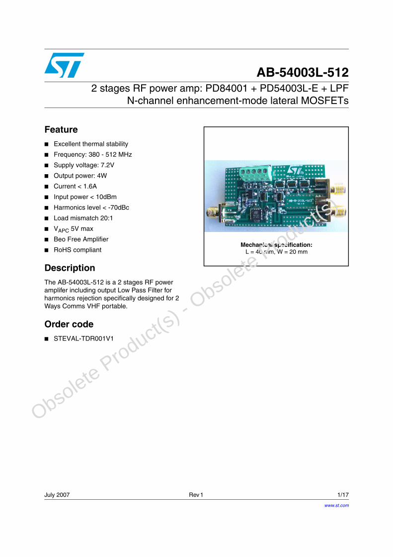
July 2007 Rev 1 1/17 17 AB-54003L-512 2 stages RF power amp: PD84001 + PD54003L-E + LPF N-channel enhancement-mode lateral MOSFETs Feature ■ Excellent thermal stability ■ Frequency: 380 - 512 MHz ■ Supply voltage: 7.2V ■ Output power: 4W ■ Current < 1.6A ■ Input power < 10dBm ■ Harmonics level < -70dBc ■ Load mismatch 20:1 ■ V APC 5V max ■ Beo Free Amplifier ■ RoHS compliant Description The AB-54003L-512 is a 2 stages RF power amplifer including output Low Pass Filter for harmonics rejection specifically designed for 2 Ways Comms VHF portable. Order code ■ STEVAL-TDR001V1 Mechanical specification: L = 40 mm, W = 20 mm www.st.com Obsolete Product(s) - Obsolete Product(s)
Transcript
July 2007 Rev 1 1/17
17
AB-54003L-5122 stages RF power amp: PD84001 + PD54003L-E + LPF
N-channel enhancement-mode lateral MOSFETs
Feature Excellent thermal stability
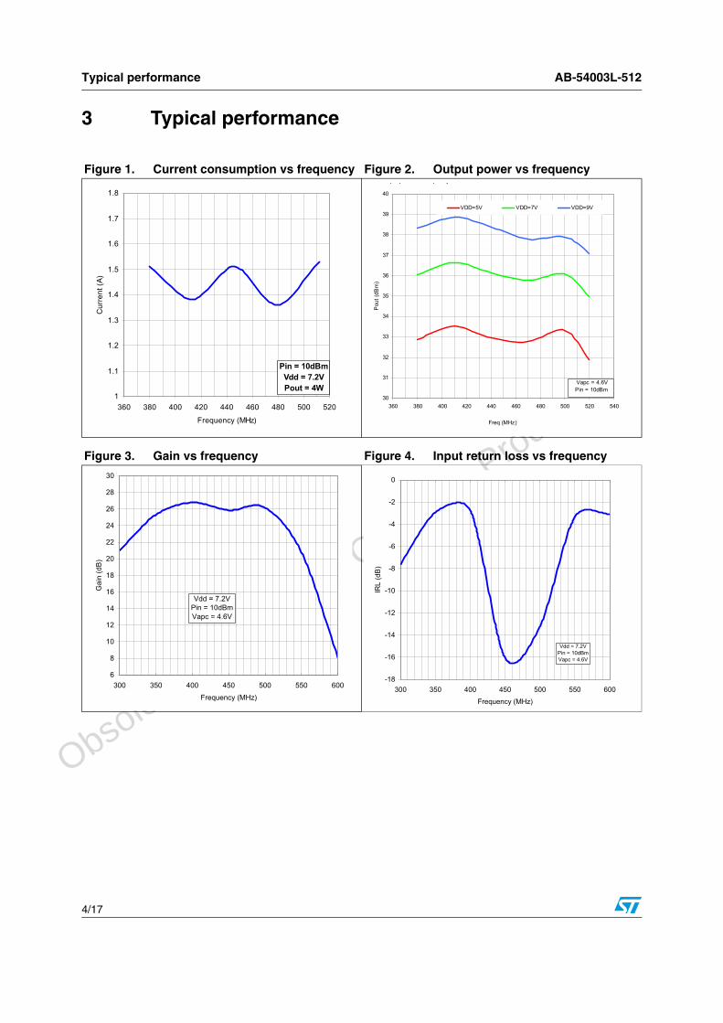
Frequency: 380 - 512 MHz
Supply voltage: 7.2V
Output power: 4W
Current < 1.6A
Input power < 10dBm
Harmonics level < -70dBc
Load mismatch 20:1
VAPC 5V max
Beo Free Amplifier
RoHS compliant
DescriptionThe AB-54003L-512 is a 2 stages RF power amplifer including output Low Pass Filter for harmonics rejection specifically designed for 2 Ways Comms VHF portable.
Designator Value Quantity Manufacturer Part code Size
C1 1 uF 1 Murata GRM1885F51C105ZA01 603
C1F 2.2 pF 1 Murata GRM1885C1H2R2CZ01 603
C2, C3, C4 120 pF 3 Murata GRM1885C1H121JA01 603
C2F, C3F 3.3 pF 2 Murata GRM1885C1H3R3CZ01 603
C4F, C5F 2.2 pF 2 Murata GRM1885C1H2R2CZ01 603
C5, C6 1 uF 2 Murata GRM1885F51C105ZA01 603
C6F 4.7 pF 1 Murata GRM1885C1H4R7CZ01 603
C7 120 nF 1 Murata GRM1885C1H121JA01 603
C7F, C8F 3.9 pF 2 Murata GRM1885C1H3R9CZ01 603
C8, C10 470 pF 2 Murata GRM1885C1H471JA01 603
C9 470 pF 1 Murata GRM1885C1H471JA01 603
C9F 1.2 pF 1 Murata GRM1885C1H1R2CZ01 603
C11 15 pF 1 Murata GRM1885C1H150JA01 603
C12 4.7 pF 1 Murata GRM1885C1H4R7CZ01 603
C13 18 pF 1 Murata GRM1885C1H180JA01 603
C14 39 pF 1 Murata GRM1885C1H390JA01 603
C15, C16 18 pF 2 Murata GRM1885C1H180JA01 603
C17 15 pF 1 Murata GRM1885C1H150JA01 603
C18 NC 1 Murata GRM1885C1H471JA01 603
DC-Con 1 Phoenix Contact 1725685 2.54mm, 5 poli
L1 24 nH 1 Coilcraft 0603HC-24NX_BW 603
L1F, L2, L2F, L3F, L4F
12.55 nH 5 Coilcraft 1606-10_, 1606_10 1606
L3, L4 3.6 nH 2 Coilcraft 0603HC-3N6X_BW 603
L5 2.55 nH 1 Coilcraft 0906-3_ 906
PD54003L 1 STMicroelectronics PD54003L-E
PD84001 1 STMicroelectronics PD84001
R1 300 1Tyco/Electronics
NeohnCRG Series Thick Film
Chip603
R2, R5 3 K 2Tyco/Electronics
NeohnCRG Series Thick Film
Chip603
R3, R6 15 2Tyco/Electronics
NeohnCRG Series Thick Film
Chip603
R4 1.5 K 1Tyco/Electronics
NeohnCRG Series Thick Film
Chip603
RF In, RF Out, RF Out PA
3
SUB 1 FR-4 H=20mil h=10oz
TL1 50 1 L=6.88mm W=0.92mm
TL2 50 1 L=9.8mm W=0.92mm
TL3 1 L=9.8mm W=0.92mm
TL4 1 50 Ω
Obsolete Product(
s) - O
bsolete Product(
s)
AB-54003L-512 Circuit layout
7/17
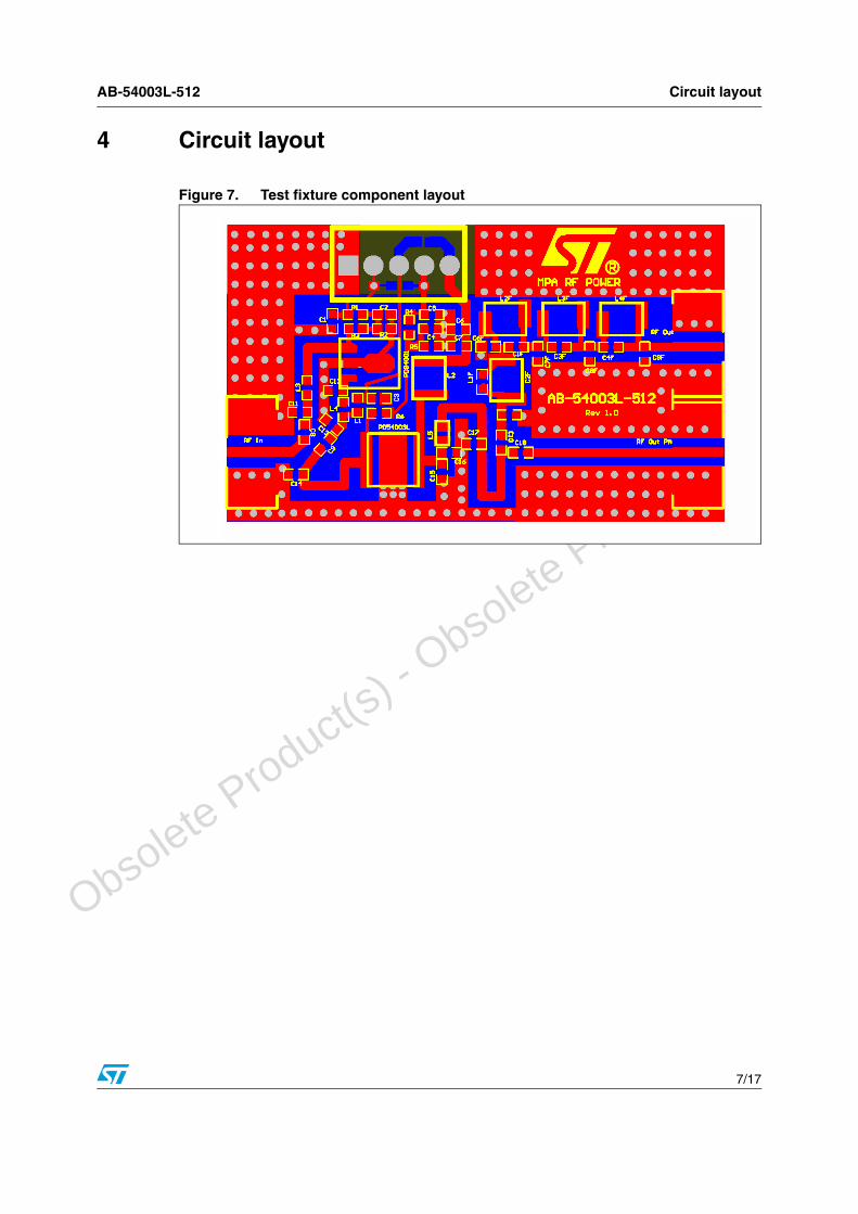
4 Circuit layout
Figure 7. Test fixture component layout
Obsolete Product(
s) - O
bsolete Product(
s)
Circuit schematic AB-54003L-512
8/17
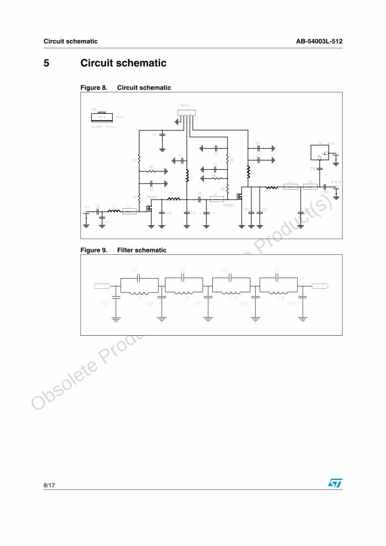
5 Circuit schematic
Figure 8. Circuit schematic
Figure 9. Filter schematic
Obsolete Product(
s) - O
bsolete Product(
s)
AB-54003L-512 Package mechanical data
9/17
6 Package mechanical data
In order to meet environmental requirements, ST offers these devices in ECOPACK® packages. These packages have a Lead-free second level interconnect . The category of second level interconnect is marked on the package and on the inner box label, in compliance with JEDEC Standard JESD97. The maximum ratings related to soldering conditions are also marked on the inner box label. ECOPACK is an ST trademark. ECOPACK specifications are available at: www.st.com
Obsolete Product(
s) - O
bsolete Product(
s)
Package mechanical data AB-54003L-512
10/17
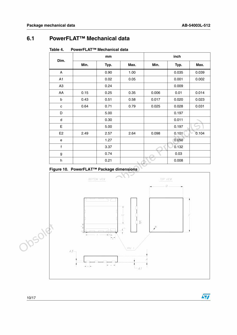
6.1 PowerFLAT™ Mechanical data
Table 4. PowerFLAT™ Mechanical data
Dim.mm inch
Min. Typ. Max. Min. Typ. Max.
A 0.90 1.00 0.035 0.039
A1 0.02 0.05 0.001 0.002
A3 0.24 0.009
AA 0.15 0.25 0.35 0.006 0.01 0.014
b 0.43 0.51 0.58 0.017 0.020 0.023
c 0.64 0.71 0.79 0.025 0.028 0.031
D 5.00 0.197
d 0.30 0.011
E 5.00 0.197
E2 2.49 2.57 2.64 0.098 0.101 0.104
e 1.27 0.050
f 3.37 0.132
g 0.74 0.03
h 0.21 0.008
Figure 10. PowerFLAT™ Package dimensions
Obsolete Product(
s) - O
bsolete Product(
s)
AB-54003L-512 Package mechanical data
11/17
Table 5. PowerFLAT™ Tape & reel dimensions
Dim.mm. inch
Min. Typ Max. Min. Typ Max.
Ao 5.15 5.25 5.35 0.12 0.13 0.13
Bo 5.15 5.25 5.35 0.12 0.13 0.13
Ko 1.0 1.1 1.2 0.02 0.02 0.02
Figure 11. PowerFLAT™ Tape & reel
Obsolete Product(
s) - O
bsolete Product(
s)
Package mechanical data AB-54003L-512
12/17
6.1.1 Mounting indications
Figure 12. Standard SMD mounting
Obsolete Product(
s) - O
bsolete Product(
s)
AB-54003L-512 Package mechanical data
13/17
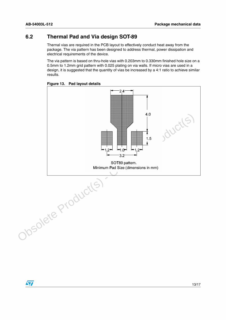
6.2 Thermal Pad and Via design SOT-89Thernal vias are required in the PCB layout to effectively conduct heat away from the package. The via pattern has been designed to address thermal, power dissipation and electrical requirements of the device.
The via pattern is based on thru-hole vias with 0.203mm to 0.330mm finished hole size on a 0.5mm to 1.2mm grid pattern with 0.025 plating on via walls. If micro vias are used in a design, it is suggested that the quantity of vias be increased by a 4:1 ratio to achieve similar results.
Figure 13. Pad layout details
Obsolete Product(
s) - O
bsolete Product(
s)
Package mechanical data AB-54003L-512
14/17
6.2.1 Soldering profile
Figure 14 shows the recommeded solder for devices that have Pb-free terminal plating and where a Pb-free solder is used.
Figure 14. Recommended solder profile
Figure 15 shows the recommeded solder for devices with Pb-free terminal plating used with leaded solder, or for devices with leaded terminal plating used with a leaded solder.
Figure 15. Recommended solder profile for leaded devices
Obsolete Product(
s) - O
bsolete Product(
s)
AB-54003L-512 Package mechanical data
15/17
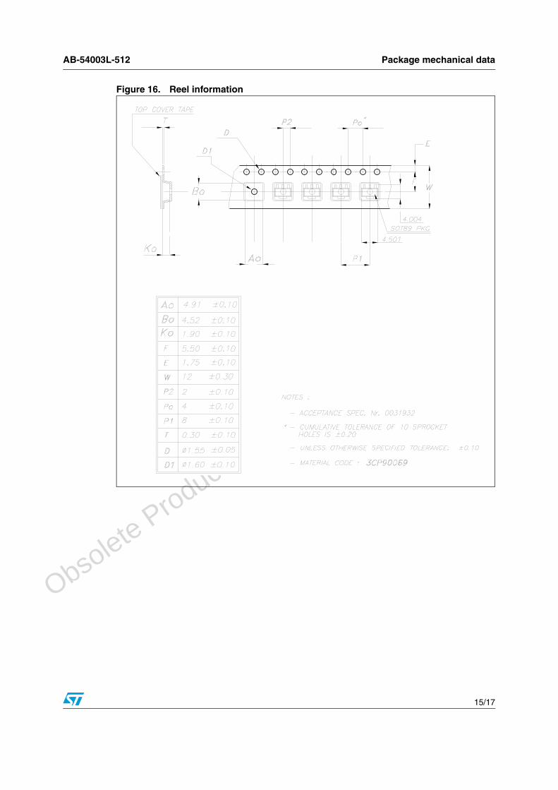
Figure 16. Reel information
Obsolete Product(
s) - O
bsolete Product(
s)
Revision history AB-54003L-512
16/17
7 Revision history
Table 6. Revision history
Date Revision Changes
18-Jul-2007 1 Initial release.
Obsolete Product(
s) - O
bsolete Product(
s)
AB-54003L-512
17/17
Please Read Carefully:
Information in this document is provided solely in connection with ST products. STMicroelectronics NV and its subsidiaries (“ST”) reserve theright to make changes, corrections, modifications or improvements, to this document, and the products and services described herein at anytime, without notice.
All ST products are sold pursuant to ST’s terms and conditions of sale.
Purchasers are solely responsible for the choice, selection and use of the ST products and services described herein, and ST assumes noliability whatsoever relating to the choice, selection or use of the ST products and services described herein.
No license, express or implied, by estoppel or otherwise, to any intellectual property rights is granted under this document. If any part of thisdocument refers to any third party products or services it shall not be deemed a license grant by ST for the use of such third party productsor services, or any intellectual property contained therein or considered as a warranty covering the use in any manner whatsoever of suchthird party products or services or any intellectual property contained therein.
UNLESS OTHERWISE SET FORTH IN ST’S TERMS AND CONDITIONS OF SALE ST DISCLAIMS ANY EXPRESS OR IMPLIEDWARRANTY WITH RESPECT TO THE USE AND/OR SALE OF ST PRODUCTS INCLUDING WITHOUT LIMITATION IMPLIEDWARRANTIES OF MERCHANTABILITY, FITNESS FOR A PARTICULAR PURPOSE (AND THEIR EQUIVALENTS UNDER THE LAWSOF ANY JURISDICTION), OR INFRINGEMENT OF ANY PATENT, COPYRIGHT OR OTHER INTELLECTUAL PROPERTY RIGHT.
UNLESS EXPRESSLY APPROVED IN WRITING BY AN AUTHORIZED ST REPRESENTATIVE, ST PRODUCTS ARE NOTRECOMMENDED, AUTHORIZED OR WARRANTED FOR USE IN MILITARY, AIR CRAFT, SPACE, LIFE SAVING, OR LIFE SUSTAININGAPPLICATIONS, NOR IN PRODUCTS OR SYSTEMS WHERE FAILURE OR MALFUNCTION MAY RESULT IN PERSONAL INJURY,DEATH, OR SEVERE PROPERTY OR ENVIRONMENTAL DAMAGE. ST PRODUCTS WHICH ARE NOT SPECIFIED AS "AUTOMOTIVEGRADE" MAY ONLY BE USED IN AUTOMOTIVE APPLICATIONS AT USER’S OWN RISK.
Resale of ST products with provisions different from the statements and/or technical features set forth in this document shall immediately voidany warranty granted by ST for the ST product or service described herein and shall not create or extend in any manner whatsoever, anyliability of ST.
ST and the ST logo are trademarks or registered trademarks of ST in various countries.
Information in this document supersedes and replaces all information previously supplied.
The ST logo is a registered trademark of STMicroelectronics. All other names are the property of their respective owners.
Australia - Belgium - Brazil - Canada - China - Czech Republic - Finland - France - Germany - Hong Kong - India - Israel - Italy - Japan - Malaysia - Malta - Morocco - Singapore - Spain - Sweden - Switzerland - United Kingdom - United States of America


![[SCORE] Opus 76 Pout-pourri (Guitar & Flute or Violin)](https://static.documents.pub/doc/80x56/5695d2781a28ab9b029a8a98/score-opus-76-pout-pourri-guitar-flute-or-violin.jpg)


