SN54LS240, SN54LS241, SN54LS244, SN54S240, SN54S241, SN54S244 SN74LS240, SN74LS241, SN74LS244, SN74S240, SN74S241, SN74S244 OCTAL BUFFERS AND LINE DRIVERS WITH 3-STATE OUTPUTS SDLS144C - APRIL 1985 - REVISED MAY 2010 1 POST OFFICE BOX 655303 • DALLAS, TEXAS 75265 D 3-State Outputs Drive Bus Lines or Buffer Memory Address Registers D PNP Inputs Reduce DC Loading D Hysteresis at Inputs Improves Noise Margins description These octal buffers and line drivers are designed specifically to improve both the performance and density of three-state memory address drivers, clock drivers, and bus-oriented receivers and transmitters. The designer has a choice of selected combinations of inverting and noninverting outputs, symmetrical, active-low output-control (G ) inputs, and complementary output-control (G and G ) inputs. These devices feature high fan-out, improved fan-in, and 400-mV noise margin. The SN74LS’ and SN74S’ devices can be used to drive terminated lines down to 133 Ω. Copyright 2010, Texas Instruments Incorporated PRODUCTION DATA information is current as of publication date. Products conform to specifications per the terms of Texas Instruments standard warranty. Production processing does not necessarily include testing of all parameters. Please be aware that an important notice concerning availability, standard warranty, and use in critical applications of Texas Instruments semiconductor products and disclaimers thereto appears at the end of this data sheet. 1 2 3 4 5 6 7 8 9 10 20 19 18 17 16 15 14 13 12 11 1G 1A1 2Y4 1A2 2Y3 1A3 2Y2 1A4 2Y1 GND V CC 2G /2G † 1Y1 2A4 1Y2 2A3 1Y3 2A2 1Y4 2A1 SN54LS’, SN54S’ . . . J OR W PACKAGE SN74LS240, SN74LS244 . . . DB, DW, N, OR NS PACKAGE SN74LS241 . . . DW, N, OR NS PACKAGE SN74S’ . . . DW OR N PACKAGE (TOP VIEW) 3 2 1 20 19 9 10 11 12 13 4 5 6 7 8 18 17 16 15 14 1Y1 2A4 1Y2 2A3 1Y3 1A2 2Y3 1A3 2Y2 1A4 SN54LS’, SN54S’ . . . FK PACKAGE (TOP VIEW) 2Y4 1A1 1G 1Y4 2A2 2G/2G 2Y1 GND 2A1 V CC † 2G for ’LS241 and ’S241 or 2G for all other drivers. † 2G for ’LS241 and ’S241 or 2G for all other drivers. † On products compliant to MIL-PRF-38535, all parameters are tested unless otherwise noted. On all other products, production processing does not necessarily include testing of all parameters.
OCTAL BUFFERS AND LINE DRIVERS WITH 3-STATE OUTPUTSSDLS144C − APRIL 1985 − REVISED MAY 2010
1POST OFFICE BOX 655303 • DALLAS, TEXAS 75265
3-State Outputs Drive Bus Lines or BufferMemory Address Registers
PNP Inputs Reduce DC Loading
Hysteresis at Inputs Improves NoiseMargins
description
These octal buffers and line drivers are designedspecifically to improve both the performance anddensity of three-state memory address drivers,clock drivers, and bus-oriented receivers andtransmitters. The designer has a choice ofselected combinations of inverting andnoninverting outputs, symmetrical, active-lowoutput-control (G) inputs, and complementaryoutput-control (G and G) inputs. These devicesfeature high fan-out, improved fan-in, and 400-mVnoise margin. The SN74LS’ and SN74S’ devicescan be used to drive terminated lines down to133 Ω.
Copyright 2010, Texas Instruments IncorporatedPRODUCTION DATA information is current as of publication date.Products conform to specifications per the terms of Texas Instrumentsstandard warranty. Production processing does not necessarily includetesting of all parameters.
Please be aware that an important notice concerning availability, standard warranty, and use in critical applications ofTexas Instruments semiconductor products and disclaimers thereto appears at the end of this data sheet.
1
2
3
4
5
6
7
8
9
10
20
19
18
17
16
15
14
13
12
11
1G1A12Y41A22Y31A32Y21A42Y1
GND
VCC
2G/2G†
1Y12A41Y22A31Y32A21Y42A1
SN54LS’, SN54S’ . . . J OR W PACKAGESN74LS240, SN74LS244 . . . DB, DW, N, OR NS PACKAGE
SN74LS241 . . . DW, N, OR NS PACKAGESN74S’ . . . DW OR N PACKAGE
(TOP VIEW)
3 2 1 20 19
9 10 11 12 13
4
5
6
7
8
18
17
16
15
14
1Y12A41Y22A31Y3
1A22Y31A32Y21A4
SN54LS’, SN54S’ . . . FK PACKAGE(TOP VIEW)
2Y4
1A1
1G1Y
42A
22G
/2G
2Y1
GN
D2A
1V C
C
† 2G for ’LS241 and ’S241 or 2G for all other drivers.
† 2G for ’LS241 and ’S241 or 2G for all other drivers.
†
On products compliant to MIL-PRF-38535, all parameters are testedunless otherwise noted. On all other products, productionprocessing does not necessarily include testing of all parameters.
SN54LS240, SN54LS241, SN54LS244, SN54S240, SN54S241, SN54S244SN74LS240, SN74LS241, SN74LS244, SN74S240, SN74S241, SN74S244OCTAL BUFFERS AND LINE DRIVERS WITH 3-STATE OUTPUTSSDLS144C − APRIL 1985 − REVISED MAY 2010
2 POST OFFICE BOX 655303 • DALLAS, TEXAS 75265
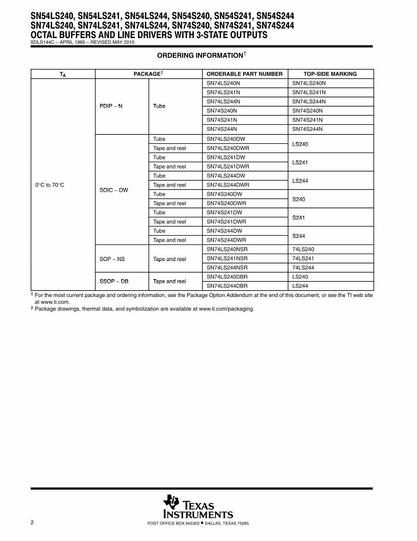
ORDERING INFORMATION
TA PACKAGE ORDERABLE PART NUMBER TOP-SIDE MARKING
SN74LS240N SN74LS240N
SN74LS241N SN74LS241N
PDIP N TubeSN74LS244N SN74LS244N
PDIP − N TubeSN74S240N SN74S240N
SN74S241N SN74S241N
SN74S244N SN74S244N
Tube SN74LS240DWLS240
Tape and reel SN74LS240DWRLS240
Tube SN74LS241DWLS241
Tape and reel SN74LS241DWRLS241
Tube SN74LS244DWLS244
0°C to 70°CSOIC DW
Tape and reel SN74LS244DWRLS244
SOIC − DWTube SN74S240DW
S240Tape and reel SN74S240DWR
S240
Tube SN74S241DWS241
Tape and reel SN74S241DWRS241
Tube SN74S244DWS244
Tape and reel SN74S244DWRS244
SN74LS240NSR 74LS240
SOP − NS Tape and reel SN74LS241NSR 74LS241SOP NS Tape and reel
SN74LS244NSR 74LS244
SSOP DB Tape and reelSN74LS240DBR LS240
SSOP − DB Tape and reelSN74LS244DBR LS244
† For the most current package and ordering information, see the Package Option Addendum at the end of this document, or see the TI web siteat www.ti.com.
‡ Package drawings, thermal data, and symbolization are available at www.ti.com/packaging.
OCTAL BUFFERS AND LINE DRIVERS WITH 3-STATE OUTPUTSSDLS144C − APRIL 1985 − REVISED MAY 2010
3POST OFFICE BOX 655303 • DALLAS, TEXAS 75265
ORDERING INFORMATION (CONTINUED)
TA PACKAGE ORDERABLE PART NUMBER TOP-SIDE MARKING
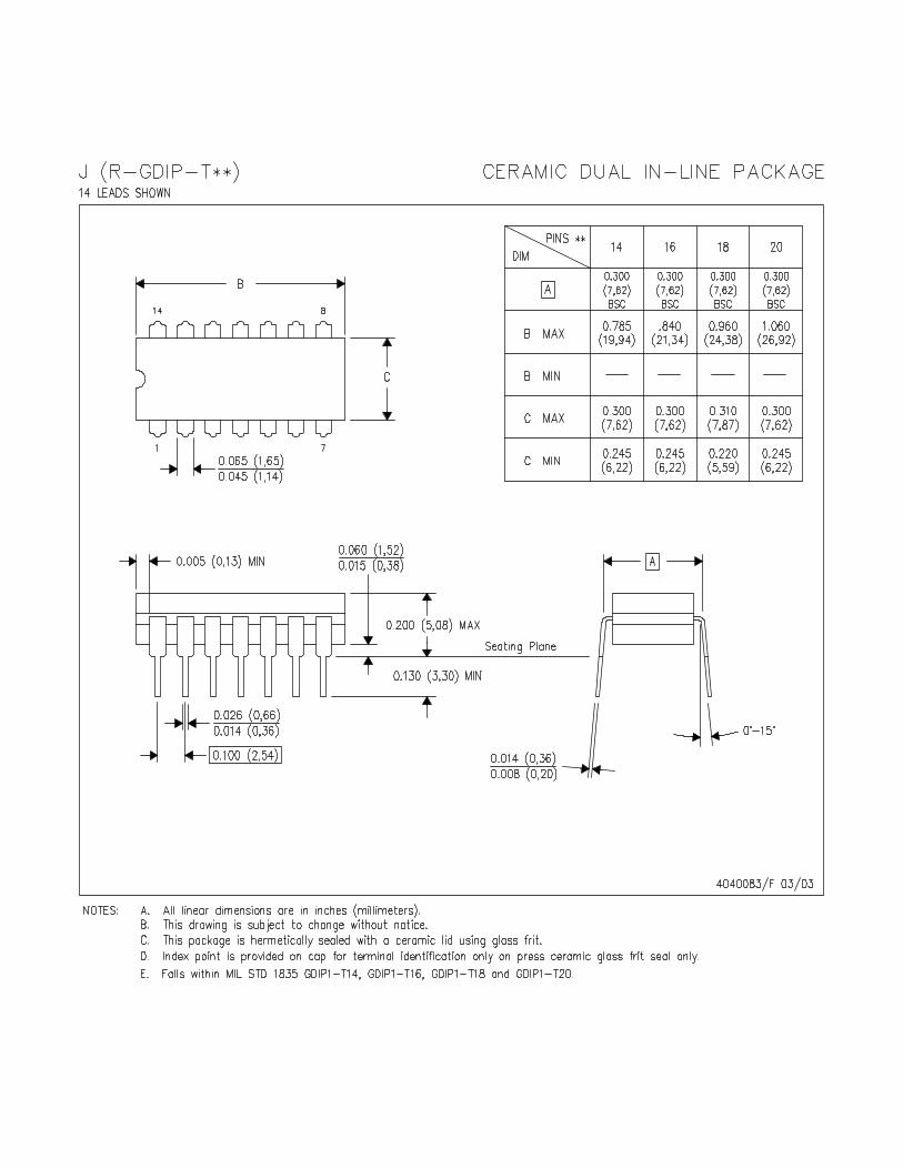
SN54LS240J SN54LS240J
SNJ54LS240J SNJ54LS240J
SN54LS241J SN54LS241J
SNJ54LS241J SNJ54LS241J
SN54LS244J SN54LS244J
CDIP J TubeSNJ54LS244J SNJ54LS244J
CDIP − J TubeSN54S240J SN54S240J
SNJ54S240J SNJ54S240J
SN54S241J SN54S241J
SNJ54S241J SNJ54S241J
SN54S244J SN54S244J
55°C to 125°CSNJ54S244J SNJ54S244J
−55°C to 125°CSNJ54LS240W SNJ54LS240W
SNJ54LS241W SNJ54LS241W
CFP W TubeSNJ54LS244W SNJ54LS244W
CFP − W TubeSNJ54S240W SNJ54S240W
SNJ54S241W SNJ54S241W
SNJ54S244W SNJ54S244W
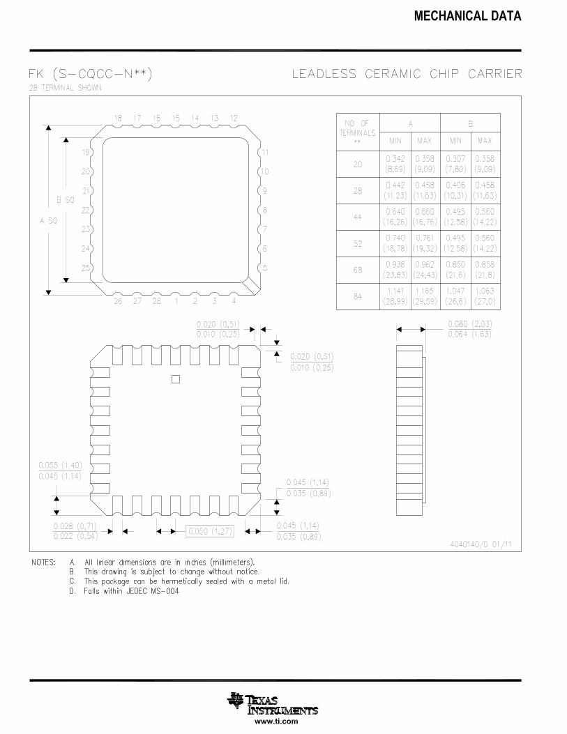
SNJ54LS240FK SNJ54LS240FK
SNJ54LS241FK SNJ54LS241FK
LCCC FK TubeSNJ54LS244FK SNJ54LS244FK
LCCC − FK TubeSNJ54S240FK SNJ54S240FK
SNJ54S241FK SNJ54S241FK
SNJ54S244FK SNJ54S244FK† For the most current package and ordering information, see the Package Option Addendum at the end of this document, or see the TI web site
at www.ti.com.‡ Package drawings, thermal data, and symbolization are available at www.ti.com/packaging.
SN54LS240, SN54LS241, SN54LS244, SN54S240, SN54S241, SN54S244SN74LS240, SN74LS241, SN74LS244, SN74S240, SN74S241, SN74S244OCTAL BUFFERS AND LINE DRIVERS WITH 3-STATE OUTPUTSSDLS144C − APRIL 1985 − REVISED MAY 2010
4 POST OFFICE BOX 655303 • DALLAS, TEXAS 75265
schematics of inputs and outputs
R
VCC
Output
TYPICAL OF ALL OUTPUTS
Req
VCC
Input
EQUIVALENT OF EACH INPUTEQUIVALENT OF EACH INPUT
9 kΩ NOM
Input
VCC
’LS240. ’LS241, ’LS244: R = 50 Ω NOM’S240, ‘S241, S244: R = 25 Ω NOM
GND
G and G inputs: Req = 2 kΩ NOMA inputs: Req = 2.8 kΩ NOM
OCTAL BUFFERS AND LINE DRIVERS WITH 3-STATE OUTPUTSSDLS144C − APRIL 1985 − REVISED MAY 2010
5POST OFFICE BOX 655303 • DALLAS, TEXAS 75265
logic diagram
1
2
4
6
8
19
11
13
15
17 3
5
7
9
12
14
16
181A1
1A2
1A3
1A4
1Y1
2A1
2A2
2A3
2A4
2Y1
1Y2
1Y3
1Y4
2Y2
2Y3
2Y4
2G
1G
’LS240, ’S240 ’LS241, ’S241
’LS244, ’S244
1
2
4
6
8
19
11
13
15
17 3
5
7
9
12
14
16
181A1
1A2
1A3
1A4
1Y1
2A1
2A2
2A3
2A4
2Y1
1Y2
1Y3
1Y4
2Y2
2Y3
2Y4
2G
1G
1
2
4
6
8
19
11
13
15
17 3
5
7
9
12
14
16
181A1
1A2
1A3
1A4
1Y1
2A1
2A2
2A3
2A4
2Y1
1Y2
1Y3
1Y4
2Y2
2Y3
2Y4
2G
1G
Pin numbers shown are for DB, DW, J, N, NS, and W packages.
SN54LS240, SN54LS241, SN54LS244, SN54S240, SN54S241, SN54S244SN74LS240, SN74LS241, SN74LS244, SN74S240, SN74S241, SN74S244OCTAL BUFFERS AND LINE DRIVERS WITH 3-STATE OUTPUTSSDLS144C − APRIL 1985 − REVISED MAY 2010
6 POST OFFICE BOX 655303 • DALLAS, TEXAS 75265
absolute maximum ratings over operating free-air temperature range (unless otherwise noted)†
Storage temperature range, Tstg −65°C to 150°C. . . . . . . . . . . . . . . . . . . . . . . . . . . . . . . . . . . . . . . . . . . . . . . . . . . † Stresses beyond those listed under “absolute maximum ratings” may cause permanent damage to the device. These are stress ratings only, and
functional operation of the device at these or any other conditions beyond those indicated under “recommended operating conditions” is notimplied. Exposure to absolute-maximum-rated conditions for extended periods may affect device reliability.
NOTES: 1. Voltage values are with respect to network ground terminal.2. The package thermal impedance is calculated in accordance with JESD 51-7.
recommended operating conditions
SN54LS’ SN74LS’UNIT
MIN NOM MAX MIN NOM MAXUNIT
VCC Supply voltage (see Note 1) 4.5 5 5.5 4.75 5 5.25 V
VIH High-level input voltage 2 2 V
VIL Low-level input voltage 0.7 0.8 V
IOH High-level output current −12 −15 mA
IOL Low-level output current 12 24 mA
TA Operating free-air temperature −55 125 0 70 °C
NOTE 1: Voltage values are with respect to network ground terminal.
OCTAL BUFFERS AND LINE DRIVERS WITH 3-STATE OUTPUTSSDLS144C − APRIL 1985 − REVISED MAY 2010
7POST OFFICE BOX 655303 • DALLAS, TEXAS 75265
electrical characteristics over recommended operating free-air temperature range (unlessotherwise noted)
PARAMETER TEST CONDITIONS†SN54LS’ SN74LS’
UNITPARAMETER TEST CONDITIONS†MIN TYP‡ MAX MIN TYP‡ MAX
UNIT
VIK VCC = MIN, II = −18 mA −1.5 −1.5 V
Hysteresis(VT+ − VT−)
VCC = MIN 0.2 0.4 0.2 0.4 V
V
VCC = MIN,IOH = −3 mA
VIH = 2 V, VIL = MAX, 2.4 3.4 2.4 3.4
VVOH VCC = MIN,IOH = MAX
VIH = 2 V, VIL = 0.5 V, 2 2V
VVCC = MIN,
V 2 VIOL = 12 mA 0.4 0.4
VVOLVCC = MIN,VIL = MAX VIH = 2 V,
IOL = 24 mA 0.5V
IOZHVCC = MAX,VIL = MAX
VIH = 2 V, VO = 2.7 V 20 20 µA
IOZLVCC = MAX,VIL = MAX
VIH = 2 V, VO = 0.4 V −20 −20 µA
II VCC = MAX, VI = 7 V 0.1 0.1 mA
IIH VCC = MAX, VI = 2.7 V 20 20 µA
IIL VCC = MAX, VIL = 0.4 V −0.2 −0.2 mA
IOS§ VCC = MAX, −40 −225 −40 −225 mA
Outputs high All 17 27 17 27
V MAX Outputs low’LS240 26 44 26 44
ICCVCC = MAX,Output open
Outputs low’LS241, ’LS244 27 46 27 46 mAICC Output open
Outputs disabled’LS240 29 50 29 50
mA
Outputs disabled’LS241, ’LS244 32 54 32 54
† For conditions shown as MIN or MAX, use the appropriate value specified under recommended operating conditions.‡ All typical values are at VCC = 5 V, TA = 25°C.§ Not more than one output should be shorted at a time, and duration of the short-circuit should not exceed one second.
switching characteristics, VCC = 5 V, TA = 25°C (see Figure 1)
PARAMETER TEST CONDITIONS’LS240 ’LS241, ’LS244
UNITPARAMETER TEST CONDITIONSMIN TYP MAX MIN TYP MAX
UNIT
tPLHR 667 Ω C 45 pF
9 14 12 18ns
tPHLRL = 667 Ω, CL = 45 pF
12 18 12 18ns
tPZLR 667 Ω C 45 F
20 30 20 30ns
tPZHRL = 667 Ω, CL = 45 pF
15 23 15 23ns
tPLZR 667 Ω C 5 pF
10 20 10 20ns
tPHZRL = 667 Ω, CL = 5 pF
15 25 15 25ns
SN54LS240, SN54LS241, SN54LS244, SN54S240, SN54S241, SN54S244SN74LS240, SN74LS241, SN74LS244, SN74S240, SN74S241, SN74S244OCTAL BUFFERS AND LINE DRIVERS WITH 3-STATE OUTPUTSSDLS144C − APRIL 1985 − REVISED MAY 2010
8 POST OFFICE BOX 655303 • DALLAS, TEXAS 75265
recommended operating conditions
SN54S’ SN74S’UNIT
MIN NOM MAX MIN NOM MAXUNIT
VCC Supply voltage (see Note 1) 4.5 5 5.5 4.75 5 5.25 V
VIH High-level input voltage 2 2 V
VIL Low-level input voltage 0.8 0.8 V
IOH High-level output current −12 −15 mA
IOL Low-level output current 48 64 mA
External resistance between any input and VCC or ground 40 40 kΩ
TA Operating free-air temperature (see Note 3) −55 125 0 70 °C
NOTES: 1. Voltage values are with respect to network ground terminal.3. An SN54S241J operating at free-air temperature above 116°C requires a heat sink that provides a thermal resistance from case
to free air, RθCA, of not more that 40°C/W.
electrical characteristics over recommended operating free-air temperature range (unlessotherwise noted)
PARAMETER TEST CONDITIONS†SN54S’ SN74S’
UNITPARAMETER TEST CONDITIONS†MIN TYP‡ MAX MIN TYP‡ MAX
UNIT
VIK VCC = MIN, II = −18 mA −1.2 −1.2 V
Hysteresis(VT+ − VT−)
VCC = MIN 0.2 0.4 0.2 0.4 V
VCC = MINIOH = −1 mA
VIH = 2 V, VIL = 0.8 V,2.7
VOHVCC = MIN,IOH = −3 mA
VIH = 2 V, VIL = 0.8 V,2.4 3.4 2.4 3.4 V
VCC = MIN,IOH = MAX
VIH = 2 V, VIL = 0.5 V,2 2
VOLVCC = MIN,IOL = MAX
VIH = 2 V, VIL = 0.8 V,0.55 0.55 V
IOZHVCC = MAX,VIL = 0.8 V
VIH = 2 V,VO = 2.4 V 50 50 µA
IOZLVCC = MAX,VIL = 0.8 V
VIH = 2 V,VO = 0.5 V −50 −50 µA
II VCC = MAX, VI = 5.5 V 1 1 mA
IIH VCC = MAX, VI = 2.7 V 50 50 µA
I V MAX V 0 5 VAny A −400 −400 µA
IIL VCC = MAX, VI = 0.5 VAny G −2 −2 mA
IOS§ VCC = MAX −50 −225 −50 −225 mA
Outputs high’S240 80 123 80 135
Outputs high’S241,’S244 95 147 95 160
IVCC = MAX,
Outputs low’S240 100 145 100 150
mAICCVCC = MAX,Output open Outputs low
’S241, ’S244 120 170 120 180mA
Outputs disabled’S240 100 145 100 150
Outputs disabled’S241, ’S244 120 170 120 180
† For conditions shown as MIN or MAX, use the appropriate value specified under recommended operating conditions.‡ All typical values are at VCC = 5 V, TA = 25°C.§ Not more than one output should be shorted at a time, and duration of the short-circuit should not exceed one second.
OCTAL BUFFERS AND LINE DRIVERS WITH 3-STATE OUTPUTSSDLS144C − APRIL 1985 − REVISED MAY 2010
9POST OFFICE BOX 655303 • DALLAS, TEXAS 75265
switching characteristics, VCC = 5 V, TA = 25°C (see Figure 2)
PARAMETER TEST CONDITIONS’S240 ’S241, ’S244
UNITPARAMETER TEST CONDITIONSMIN TYP MAX MIN TYP MAX
UNIT
tPLHR 90 Ω C 50 F
4.5 7 6 9ns
tPHLRL = 90 Ω, CL = 50 pF
4.5 7 6 9ns
tPZLR 90 Ω C 50 F
10 15 10 15ns
tPZHRL = 90 Ω, CL = 50 pF
6.5 10 8 12ns
tPLZR 90 Ω C 5 pF
10 15 10 15ns
tPHZRL = 90 Ω, CL = 5 pF
6 9 6 9ns
SN54LS240, SN54LS241, SN54LS244, SN54S240, SN54S241, SN54S244SN74LS240, SN74LS241, SN74LS244, SN74S240, SN74S241, SN74S244OCTAL BUFFERS AND LINE DRIVERS WITH 3-STATE OUTPUTSSDLS144C − APRIL 1985 − REVISED MAY 2010
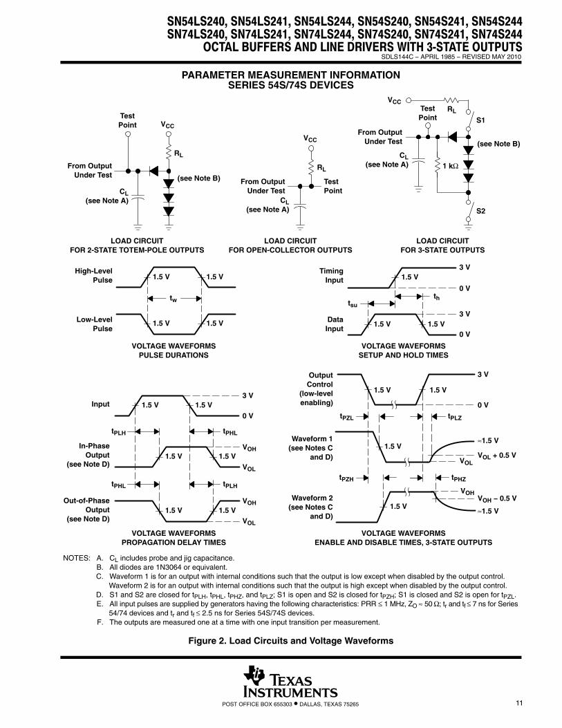
NOTES: A. CL includes probe and jig capacitance.B. All diodes are 1N3064 or equivalent.C. Waveform 1 is for an output with internal conditions such that the output is low except when disabled by the output control.
Waveform 2 is for an output with internal conditions such that the output is high except when disabled by the output control.D. S1 and S2 are closed for tPLH, tPHL, tPHZ, and tPLZ; S1 is open and S2 is closed for tPZH; S1 is closed and S2 is open for tPZL.E. Phase relationships between inputs and outputs have been chosen arbitrarily for these examples.F. All input pulses are supplied by generators having the following characteristics: PRR ≤ 1 MHz, ZO ≈ 50 Ω, tr ≤ 15 ns, tf ≤ 6 ns.G. The outputs are measured one at a time with one input transition per measurement.
S1
S2
tPHZ
tPLZtPZL
tPZH
3 V
3 V
0 V
0 V
thtsu
VOLTAGE WAVEFORMSSETUP AND HOLD TIMES
TimingInput
DataInput
3 V
0 V
OutputControl
(low-levelenabling)
Waveform 1(see Notes C
and D)
Waveform 2(see Notes C
and D) ≈1.5 V
VOH − 0.3 V
VOL + 0.3 V
≈1.5 V
VOLTAGE WAVEFORMSENABLE AND DISABLE TIMES, 3-STATE OUTPUTS
NOTES: A. CL includes probe and jig capacitance.B. All diodes are 1N3064 or equivalent.C. Waveform 1 is for an output with internal conditions such that the output is low except when disabled by the output control.
Waveform 2 is for an output with internal conditions such that the output is high except when disabled by the output control.D. S1 and S2 are closed for tPLH, tPHL, tPHZ, and tPLZ; S1 is open and S2 is closed for tPZH; S1 is closed and S2 is open for tPZL.E. All input pulses are supplied by generators having the following characteristics: PRR ≤ 1 MHz, ZO ≈ 50 Ω; tr and tf ≤ 7 ns for Series
54/74 devices and tr and tf ≤ 2.5 ns for Series 54S/74S devices.F. The outputs are measured one at a time with one input transition per measurement.
S1
S2
tPHZ
tPLZtPZL
tPZH
3 V
3 V
0 V
0 V
thtsu
VOLTAGE WAVEFORMSSETUP AND HOLD TIMES
TimingInput
DataInput
3 V
0 V
OutputControl
(low-levelenabling)
Waveform 1(see Notes C
and D)
Waveform 2(see Notes C
and D)≈1.5 V
VOH − 0.5 V
VOL + 0.5 V
≈1.5 V
VOLTAGE WAVEFORMSENABLE AND DISABLE TIMES, 3-STATE OUTPUTS
1.5 V 1.5 V
1.5 V 1.5 V
1.5 V
1.5 V 1.5 V
1.5 V 1.5 V
1.5 V
1.5 V
tw
1.5 V 1.5 V
1.5 V 1.5 V
1.5 V 1.5 V
VOH
VOL
Figure 2. Load Circuits and Voltage Waveforms
SN54LS240, SN54LS241, SN54LS244, SN54S240, SN54S241, SN54S244SN74LS240, SN74LS241, SN74LS244, SN74S240, SN74S241, SN74S244OCTAL BUFFERS AND LINE DRIVERS WITH 3-STATE OUTPUTSSDLS144C − APRIL 1985 − REVISED MAY 2010
12 POST OFFICE BOX 655303 • DALLAS, TEXAS 75265
APPLICATION INFORMATION
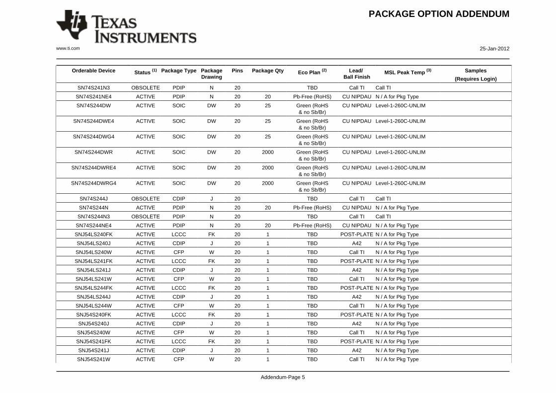
PACKAGE OPTION ADDENDUM
www.ti.com 25-Jan-2012
Addendum-Page 1
PACKAGING INFORMATION
Orderable Device Status (1) Package Type PackageDrawing
Pins Package Qty Eco Plan (2) Lead/Ball Finish
MSL Peak Temp (3) Samples
(Requires Login)
5962-7801201VRA ACTIVE CDIP J 20 1 TBD A42 N / A for Pkg Type
5962-7801201VSA ACTIVE CFP W 20 1 TBD Call TI N / A for Pkg Type
7705701RA ACTIVE CDIP J 20 1 TBD Call TI Call TI
7705701SA ACTIVE CFP W 20 1 TBD Call TI Call TI
78012012A ACTIVE LCCC FK 20 1 TBD Call TI Call TI
7801201RA ACTIVE CDIP J 20 1 TBD Call TI Call TI
7801201SA ACTIVE CFP W 20 1 TBD Call TI Call TI
JM38510/32401B2A ACTIVE LCCC FK 20 1 TBD POST-PLATE N / A for Pkg Type
JM38510/32401BRA ACTIVE CDIP J 20 1 TBD A42 N / A for Pkg Type
JM38510/32401BSA ACTIVE CFP W 20 1 TBD Call TI N / A for Pkg Type
JM38510/32402B2A ACTIVE LCCC FK 20 1 TBD POST-PLATE N / A for Pkg Type
JM38510/32402BRA ACTIVE CDIP J 20 1 TBD A42 N / A for Pkg Type
JM38510/32402BSA ACTIVE CFP W 20 1 TBD Call TI N / A for Pkg Type
JM38510/32403B2A ACTIVE LCCC FK 20 1 TBD POST-PLATE N / A for Pkg Type
JM38510/32403BRA ACTIVE CDIP J 20 1 TBD A42 N / A for Pkg Type
JM38510/32403BSA ACTIVE CFP W 20 1 TBD Call TI N / A for Pkg Type
JM38510/32403SRA ACTIVE CDIP J 20 1 TBD A42 N / A for Pkg Type
JM38510/32403SSA ACTIVE CFP W 20 1 TBD Call TI N / A for Pkg Type
M38510/32401B2A ACTIVE LCCC FK 20 1 TBD POST-PLATE N / A for Pkg Type
M38510/32401BRA ACTIVE CDIP J 20 1 TBD A42 N / A for Pkg Type
M38510/32401BSA ACTIVE CFP W 20 1 TBD Call TI N / A for Pkg Type
M38510/32402B2A ACTIVE LCCC FK 20 1 TBD POST-PLATE N / A for Pkg Type
M38510/32402BRA ACTIVE CDIP J 20 1 TBD A42 N / A for Pkg Type
M38510/32402BSA ACTIVE CFP W 20 1 TBD Call TI N / A for Pkg Type
M38510/32403B2A ACTIVE LCCC FK 20 1 TBD POST-PLATE N / A for Pkg Type
M38510/32403BRA ACTIVE CDIP J 20 1 TBD A42 N / A for Pkg Type
M38510/32403BSA ACTIVE CFP W 20 1 TBD Call TI N / A for Pkg Type
M38510/32403SRA ACTIVE CDIP J 20 1 TBD A42 N / A for Pkg Type
M38510/32403SSA ACTIVE CFP W 20 1 TBD Call TI N / A for Pkg Type
SN54LS240J ACTIVE CDIP J 20 1 TBD A42 N / A for Pkg Type
PACKAGE OPTION ADDENDUM
www.ti.com 25-Jan-2012
Addendum-Page 2
Orderable Device Status (1) Package Type PackageDrawing
Pins Package Qty Eco Plan (2) Lead/Ball Finish
MSL Peak Temp (3) Samples
(Requires Login)
SN54LS241J ACTIVE CDIP J 20 1 TBD A42 N / A for Pkg Type
SN54LS244J ACTIVE CDIP J 20 1 TBD A42 N / A for Pkg Type
SN54S240J ACTIVE CDIP J 20 1 TBD A42 N / A for Pkg Type
SN54S241J ACTIVE CDIP J 20 1 TBD A42 N / A for Pkg Type
SN54S244J ACTIVE CDIP J 20 1 TBD A42 N / A for Pkg Type
SN74LS240DW ACTIVE SOIC DW 20 25 Green (RoHS& no Sb/Br)
CU NIPDAU Level-1-260C-UNLIM
SN74LS240DWG4 ACTIVE SOIC DW 20 25 Green (RoHS& no Sb/Br)
CU NIPDAU Level-1-260C-UNLIM
SN74LS240DWR ACTIVE SOIC DW 20 2000 Green (RoHS& no Sb/Br)
CU NIPDAU Level-1-260C-UNLIM
SN74LS240DWRE4 ACTIVE SOIC DW 20 2000 Green (RoHS& no Sb/Br)
CU NIPDAU Level-1-260C-UNLIM
SN74LS240DWRG4 ACTIVE SOIC DW 20 2000 Green (RoHS& no Sb/Br)
CU NIPDAU Level-1-260C-UNLIM
SN74LS240J OBSOLETE CDIP J 20 TBD Call TI Call TI
SN74LS240N ACTIVE PDIP N 20 20 Pb-Free (RoHS) CU NIPDAU N / A for Pkg Type
SN74LS240N3 OBSOLETE PDIP N 20 TBD Call TI Call TI
SN74LS240NE4 ACTIVE PDIP N 20 20 Pb-Free (RoHS) CU NIPDAU N / A for Pkg Type
SN74LS240NSR ACTIVE SO NS 20 2000 Green (RoHS& no Sb/Br)
CU NIPDAU Level-1-260C-UNLIM
SN74LS240NSRE4 ACTIVE SO NS 20 2000 Green (RoHS& no Sb/Br)
CU NIPDAU Level-1-260C-UNLIM
SN74LS240NSRG4 ACTIVE SO NS 20 2000 Green (RoHS& no Sb/Br)
CU NIPDAU Level-1-260C-UNLIM
SN74LS241DW ACTIVE SOIC DW 20 25 Green (RoHS& no Sb/Br)
CU NIPDAU Level-1-260C-UNLIM
SN74LS241DWE4 ACTIVE SOIC DW 20 25 Green (RoHS& no Sb/Br)
CU NIPDAU Level-1-260C-UNLIM
SN74LS241DWG4 ACTIVE SOIC DW 20 25 Green (RoHS& no Sb/Br)
CU NIPDAU Level-1-260C-UNLIM
SN74LS241DWR ACTIVE SOIC DW 20 2000 Green (RoHS& no Sb/Br)
CU NIPDAU Level-1-260C-UNLIM
SN74LS241DWRE4 ACTIVE SOIC DW 20 2000 Green (RoHS& no Sb/Br)
CU NIPDAU Level-1-260C-UNLIM
PACKAGE OPTION ADDENDUM
www.ti.com 25-Jan-2012
Addendum-Page 3
Orderable Device Status (1) Package Type PackageDrawing
Pins Package Qty Eco Plan (2) Lead/Ball Finish
MSL Peak Temp (3) Samples
(Requires Login)
SN74LS241DWRG4 ACTIVE SOIC DW 20 2000 Green (RoHS& no Sb/Br)
CU NIPDAU Level-1-260C-UNLIM
SN74LS241J OBSOLETE CDIP J 20 TBD Call TI Call TI
SN74LS241N ACTIVE PDIP N 20 20 Pb-Free (RoHS) CU NIPDAU N / A for Pkg Type
SN74LS241N3 OBSOLETE PDIP N 20 TBD Call TI Call TI
SN74LS241NE4 ACTIVE PDIP N 20 20 Pb-Free (RoHS) CU NIPDAU N / A for Pkg Type
SN74LS241NSR ACTIVE SO NS 20 2000 Green (RoHS& no Sb/Br)
CU NIPDAU Level-1-260C-UNLIM
SN74LS241NSRE4 ACTIVE SO NS 20 2000 Green (RoHS& no Sb/Br)
CU NIPDAU Level-1-260C-UNLIM
SN74LS241NSRG4 ACTIVE SO NS 20 2000 Green (RoHS& no Sb/Br)
CU NIPDAU Level-1-260C-UNLIM
SN74LS244DBR ACTIVE SSOP DB 20 2000 Green (RoHS& no Sb/Br)
CU NIPDAU Level-1-260C-UNLIM
SN74LS244DBRE4 ACTIVE SSOP DB 20 2000 Green (RoHS& no Sb/Br)
CU NIPDAU Level-1-260C-UNLIM
SN74LS244DBRG4 ACTIVE SSOP DB 20 2000 Green (RoHS& no Sb/Br)
CU NIPDAU Level-1-260C-UNLIM
SN74LS244DW ACTIVE SOIC DW 20 25 Green (RoHS& no Sb/Br)
CU NIPDAU Level-1-260C-UNLIM
SN74LS244DWE4 ACTIVE SOIC DW 20 25 Green (RoHS& no Sb/Br)
CU NIPDAU Level-1-260C-UNLIM
SN74LS244DWG4 ACTIVE SOIC DW 20 25 Green (RoHS& no Sb/Br)
CU NIPDAU Level-1-260C-UNLIM
SN74LS244DWR ACTIVE SOIC DW 20 2000 Green (RoHS& no Sb/Br)
CU NIPDAU Level-1-260C-UNLIM
SN74LS244DWRE4 ACTIVE SOIC DW 20 2000 Green (RoHS& no Sb/Br)
CU NIPDAU Level-1-260C-UNLIM
SN74LS244DWRG4 ACTIVE SOIC DW 20 2000 Green (RoHS& no Sb/Br)
CU NIPDAU Level-1-260C-UNLIM
SN74LS244J OBSOLETE CDIP J 20 TBD Call TI Call TI
SN74LS244N ACTIVE PDIP N 20 20 Pb-Free (RoHS) CU NIPDAU N / A for Pkg Type
SN74LS244N3 OBSOLETE PDIP N 20 TBD Call TI Call TI
SN74LS244NE4 ACTIVE PDIP N 20 20 Pb-Free (RoHS) CU NIPDAU N / A for Pkg Type
PACKAGE OPTION ADDENDUM
www.ti.com 25-Jan-2012
Addendum-Page 4
Orderable Device Status (1) Package Type PackageDrawing
Pins Package Qty Eco Plan (2) Lead/Ball Finish
MSL Peak Temp (3) Samples
(Requires Login)
SN74LS244NSR ACTIVE SO NS 20 2000 Green (RoHS& no Sb/Br)
CU NIPDAU Level-1-260C-UNLIM
SN74LS244NSRE4 ACTIVE SO NS 20 2000 Green (RoHS& no Sb/Br)
CU NIPDAU Level-1-260C-UNLIM
SN74LS244NSRG4 ACTIVE SO NS 20 2000 Green (RoHS& no Sb/Br)
CU NIPDAU Level-1-260C-UNLIM
SN74S240DW ACTIVE SOIC DW 20 25 Green (RoHS& no Sb/Br)
CU NIPDAU Level-1-260C-UNLIM
SN74S240DWE4 ACTIVE SOIC DW 20 25 Green (RoHS& no Sb/Br)
CU NIPDAU Level-1-260C-UNLIM
SN74S240DWG4 ACTIVE SOIC DW 20 25 Green (RoHS& no Sb/Br)
CU NIPDAU Level-1-260C-UNLIM
SN74S240DWR ACTIVE SOIC DW 20 2000 Green (RoHS& no Sb/Br)
CU NIPDAU Level-1-260C-UNLIM
SN74S240DWRE4 ACTIVE SOIC DW 20 2000 Green (RoHS& no Sb/Br)
CU NIPDAU Level-1-260C-UNLIM
SN74S240DWRG4 ACTIVE SOIC DW 20 2000 Green (RoHS& no Sb/Br)
CU NIPDAU Level-1-260C-UNLIM
SN74S240N ACTIVE PDIP N 20 20 Pb-Free (RoHS) CU NIPDAU N / A for Pkg Type
SN74S240N3 OBSOLETE PDIP N 20 TBD Call TI Call TI
SN74S240NE4 ACTIVE PDIP N 20 20 Pb-Free (RoHS) CU NIPDAU N / A for Pkg Type
SN74S241DW ACTIVE SOIC DW 20 25 Green (RoHS& no Sb/Br)
CU NIPDAU Level-1-260C-UNLIM
SN74S241DWE4 ACTIVE SOIC DW 20 25 Green (RoHS& no Sb/Br)
CU NIPDAU Level-1-260C-UNLIM
SN74S241DWG4 ACTIVE SOIC DW 20 25 Green (RoHS& no Sb/Br)
CU NIPDAU Level-1-260C-UNLIM
SN74S241DWR ACTIVE SOIC DW 20 2000 Green (RoHS& no Sb/Br)
CU NIPDAU Level-1-260C-UNLIM
SN74S241DWRE4 ACTIVE SOIC DW 20 2000 Green (RoHS& no Sb/Br)
CU NIPDAU Level-1-260C-UNLIM
SN74S241DWRG4 ACTIVE SOIC DW 20 2000 Green (RoHS& no Sb/Br)
CU NIPDAU Level-1-260C-UNLIM
SN74S241J OBSOLETE CDIP J 20 TBD Call TI Call TI
SN74S241N ACTIVE PDIP N 20 20 Pb-Free (RoHS) CU NIPDAU N / A for Pkg Type
PACKAGE OPTION ADDENDUM
www.ti.com 25-Jan-2012
Addendum-Page 5
Orderable Device Status (1) Package Type PackageDrawing
Pins Package Qty Eco Plan (2) Lead/Ball Finish
MSL Peak Temp (3) Samples
(Requires Login)
SN74S241N3 OBSOLETE PDIP N 20 TBD Call TI Call TI
SN74S241NE4 ACTIVE PDIP N 20 20 Pb-Free (RoHS) CU NIPDAU N / A for Pkg Type
SN74S244DW ACTIVE SOIC DW 20 25 Green (RoHS& no Sb/Br)
CU NIPDAU Level-1-260C-UNLIM
SN74S244DWE4 ACTIVE SOIC DW 20 25 Green (RoHS& no Sb/Br)
CU NIPDAU Level-1-260C-UNLIM
SN74S244DWG4 ACTIVE SOIC DW 20 25 Green (RoHS& no Sb/Br)
CU NIPDAU Level-1-260C-UNLIM
SN74S244DWR ACTIVE SOIC DW 20 2000 Green (RoHS& no Sb/Br)
CU NIPDAU Level-1-260C-UNLIM
SN74S244DWRE4 ACTIVE SOIC DW 20 2000 Green (RoHS& no Sb/Br)
CU NIPDAU Level-1-260C-UNLIM
SN74S244DWRG4 ACTIVE SOIC DW 20 2000 Green (RoHS& no Sb/Br)
CU NIPDAU Level-1-260C-UNLIM
SN74S244J OBSOLETE CDIP J 20 TBD Call TI Call TI
SN74S244N ACTIVE PDIP N 20 20 Pb-Free (RoHS) CU NIPDAU N / A for Pkg Type
SN74S244N3 OBSOLETE PDIP N 20 TBD Call TI Call TI
SN74S244NE4 ACTIVE PDIP N 20 20 Pb-Free (RoHS) CU NIPDAU N / A for Pkg Type
SNJ54LS240FK ACTIVE LCCC FK 20 1 TBD POST-PLATE N / A for Pkg Type
SNJ54LS240J ACTIVE CDIP J 20 1 TBD A42 N / A for Pkg Type
SNJ54LS240W ACTIVE CFP W 20 1 TBD Call TI N / A for Pkg Type
SNJ54LS241FK ACTIVE LCCC FK 20 1 TBD POST-PLATE N / A for Pkg Type
SNJ54LS241J ACTIVE CDIP J 20 1 TBD A42 N / A for Pkg Type
SNJ54LS241W ACTIVE CFP W 20 1 TBD Call TI N / A for Pkg Type
SNJ54LS244FK ACTIVE LCCC FK 20 1 TBD POST-PLATE N / A for Pkg Type
SNJ54LS244J ACTIVE CDIP J 20 1 TBD A42 N / A for Pkg Type
SNJ54LS244W ACTIVE CFP W 20 1 TBD Call TI N / A for Pkg Type
SNJ54S240FK ACTIVE LCCC FK 20 1 TBD POST-PLATE N / A for Pkg Type
SNJ54S240J ACTIVE CDIP J 20 1 TBD A42 N / A for Pkg Type
SNJ54S240W ACTIVE CFP W 20 1 TBD Call TI N / A for Pkg Type
SNJ54S241FK ACTIVE LCCC FK 20 1 TBD POST-PLATE N / A for Pkg Type
SNJ54S241J ACTIVE CDIP J 20 1 TBD A42 N / A for Pkg Type
SNJ54S241W ACTIVE CFP W 20 1 TBD Call TI N / A for Pkg Type
PACKAGE OPTION ADDENDUM
www.ti.com 25-Jan-2012
Addendum-Page 6
Orderable Device Status (1) Package Type PackageDrawing
Pins Package Qty Eco Plan (2) Lead/Ball Finish
MSL Peak Temp (3) Samples
(Requires Login)
SNJ54S244FK ACTIVE LCCC FK 20 1 TBD POST-PLATE N / A for Pkg Type
SNJ54S244J ACTIVE CDIP J 20 1 TBD A42 N / A for Pkg Type
SNJ54S244W ACTIVE CFP W 20 1 TBD Call TI N / A for Pkg Type (1) The marketing status values are defined as follows:ACTIVE: Product device recommended for new designs.LIFEBUY: TI has announced that the device will be discontinued, and a lifetime-buy period is in effect.NRND: Not recommended for new designs. Device is in production to support existing customers, but TI does not recommend using this part in a new design.PREVIEW: Device has been announced but is not in production. Samples may or may not be available.OBSOLETE: TI has discontinued the production of the device.
(2) Eco Plan - The planned eco-friendly classification: Pb-Free (RoHS), Pb-Free (RoHS Exempt), or Green (RoHS & no Sb/Br) - please check http://www.ti.com/productcontent for the latest availabilityinformation and additional product content details.TBD: The Pb-Free/Green conversion plan has not been defined.Pb-Free (RoHS): TI's terms "Lead-Free" or "Pb-Free" mean semiconductor products that are compatible with the current RoHS requirements for all 6 substances, including the requirement thatlead not exceed 0.1% by weight in homogeneous materials. Where designed to be soldered at high temperatures, TI Pb-Free products are suitable for use in specified lead-free processes.Pb-Free (RoHS Exempt): This component has a RoHS exemption for either 1) lead-based flip-chip solder bumps used between the die and package, or 2) lead-based die adhesive used betweenthe die and leadframe. The component is otherwise considered Pb-Free (RoHS compatible) as defined above.Green (RoHS & no Sb/Br): TI defines "Green" to mean Pb-Free (RoHS compatible), and free of Bromine (Br) and Antimony (Sb) based flame retardants (Br or Sb do not exceed 0.1% by weightin homogeneous material)
(3) MSL, Peak Temp. -- The Moisture Sensitivity Level rating according to the JEDEC industry standard classifications, and peak solder temperature.
Important Information and Disclaimer:The information provided on this page represents TI's knowledge and belief as of the date that it is provided. TI bases its knowledge and belief on informationprovided by third parties, and makes no representation or warranty as to the accuracy of such information. Efforts are underway to better integrate information from third parties. TI has taken andcontinues to take reasonable steps to provide representative and accurate information but may not have conducted destructive testing or chemical analysis on incoming materials and chemicals.TI and TI suppliers consider certain information to be proprietary, and thus CAS numbers and other limited information may not be available for release.
In no event shall TI's liability arising out of such information exceed the total purchase price of the TI part(s) at issue in this document sold by TI to Customer on an annual basis.
OTHER QUALIFIED VERSIONS OF SN54LS240, SN54LS240-SP, SN54LS241, SN54LS244, SN54LS244-SP, SN54S240, SN54S241, SN54S244, SN74LS240,SN74LS241, SN74LS244, SN74S240, SN74S241, SN74S244 :
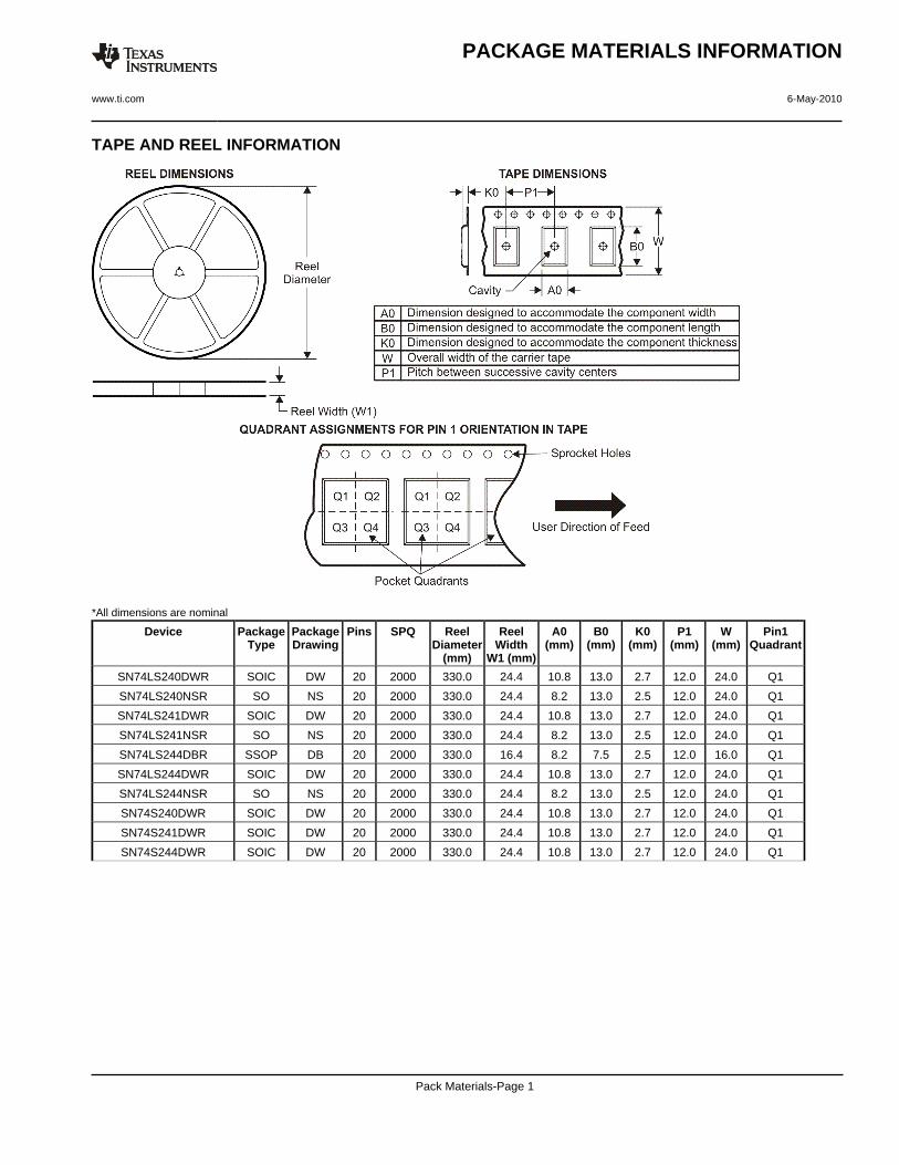
NOTES: A. All linear dimensions are in millimeters.B. This drawing is subject to change without notice.C. Body dimensions do not include mold flash or protrusion not to exceed 0,15.D. Falls within JEDEC MO-150
IMPORTANT NOTICE
Texas Instruments Incorporated and its subsidiaries (TI) reserve the right to make corrections, modifications, enhancements, improvements,and other changes to its products and services at any time and to discontinue any product or service without notice. Customers shouldobtain the latest relevant information before placing orders and should verify that such information is current and complete. All products aresold subject to TI’s terms and conditions of sale supplied at the time of order acknowledgment.
TI warrants performance of its hardware products to the specifications applicable at the time of sale in accordance with TI’s standardwarranty. Testing and other quality control techniques are used to the extent TI deems necessary to support this warranty. Except wheremandated by government requirements, testing of all parameters of each product is not necessarily performed.
TI assumes no liability for applications assistance or customer product design. Customers are responsible for their products andapplications using TI components. To minimize the risks associated with customer products and applications, customers should provideadequate design and operating safeguards.
TI does not warrant or represent that any license, either express or implied, is granted under any TI patent right, copyright, mask work right,or other TI intellectual property right relating to any combination, machine, or process in which TI products or services are used. Informationpublished by TI regarding third-party products or services does not constitute a license from TI to use such products or services or awarranty or endorsement thereof. Use of such information may require a license from a third party under the patents or other intellectualproperty of the third party, or a license from TI under the patents or other intellectual property of TI.
Reproduction of TI information in TI data books or data sheets is permissible only if reproduction is without alteration and is accompaniedby all associated warranties, conditions, limitations, and notices. Reproduction of this information with alteration is an unfair and deceptivebusiness practice. TI is not responsible or liable for such altered documentation. Information of third parties may be subject to additionalrestrictions.
Resale of TI products or services with statements different from or beyond the parameters stated by TI for that product or service voids allexpress and any implied warranties for the associated TI product or service and is an unfair and deceptive business practice. TI is notresponsible or liable for any such statements.
TI products are not authorized for use in safety-critical applications (such as life support) where a failure of the TI product would reasonablybe expected to cause severe personal injury or death, unless officers of the parties have executed an agreement specifically governingsuch use. Buyers represent that they have all necessary expertise in the safety and regulatory ramifications of their applications, andacknowledge and agree that they are solely responsible for all legal, regulatory and safety-related requirements concerning their productsand any use of TI products in such safety-critical applications, notwithstanding any applications-related information or support that may beprovided by TI. Further, Buyers must fully indemnify TI and its representatives against any damages arising out of the use of TI products insuch safety-critical applications.
TI products are neither designed nor intended for use in military/aerospace applications or environments unless the TI products arespecifically designated by TI as military-grade or "enhanced plastic." Only products designated by TI as military-grade meet militaryspecifications. Buyers acknowledge and agree that any such use of TI products which TI has not designated as military-grade is solely atthe Buyer's risk, and that they are solely responsible for compliance with all legal and regulatory requirements in connection with such use.
TI products are neither designed nor intended for use in automotive applications or environments unless the specific TI products aredesignated by TI as compliant with ISO/TS 16949 requirements. Buyers acknowledge and agree that, if they use any non-designatedproducts in automotive applications, TI will not be responsible for any failure to meet such requirements.
Following are URLs where you can obtain information on other Texas Instruments products and application solutions:
Products Applications
Audio www.ti.com/audio Automotive and Transportation www.ti.com/automotive
Amplifiers amplifier.ti.com Communications and Telecom www.ti.com/communications
Data Converters dataconverter.ti.com Computers and Peripherals www.ti.com/computers