OFDM BASED MIMO TESTING FOR RF ICs
GOPALA KRISHNA.M *1, UMA SANKAR.CH 2, PHANI KUMAR.Y 3, PAVAN KUMAR .V.G4
1, 2 Electronics & Communication Department, RK College of Engineering, Vijayawada, A.P, India
3 Electronics & Communication Department, Amrita Sai Institute of Science & Technology,
Vijayawada, A.P, India
4 Electronics & Communication Department, Sri Sunflower College of Engg. & Tech., Machilipatnam,
A.P, India
[email protected]
[email protected]
[email protected]
4 [email protected]
ABSTRACT
Multiple-input–multiple-output (MIMO)-based systems are extremely popular as they offer data
rates as twice as fast as currently available systems. Their testing becomes more complicated due to the
increased number of RF paths. This increases the overall test cost of these devices both in terms of test
time and instrumentation cost. In this paper, we demonstrate a low cost MIMO test solution which
targets critical specifications that are fundamental to the MIMO system operation, such as gain, IIP3, and
phase imbalances between the RF paths. Our test methodology measures these parameters with a single
test setup that enables the calculation of these performance parameters. Using the proposed test method,
RF MIMO systems can be tested using a mixed signal tester, and on-board circuitry within a reasonable
accuracy. Both simulation and measurement results confirm the high accuracy and repeatability of our
test technique.
KEY WORDS — Multiple, input, Spectrum, Analyzer, MIMO, RF testi ng, OFDM, WLAN.
I. INTRODUCTION
RECENTLY, multiple-input–multiple-output (MIMO) communications systems that contain
multiple RF paths are reported to increase the spectral efficiency and to improve the link reliability
without increasing the bandwidth. However, the increase in the number of RF paths also translates as
increased test time and instrumentation costs. Moreover, additional performance metrics that are
necessary to characterize the MIMO operation, such as mismatch parameters between the RF branches
of the transceiver, need to be tested to meet the stringent specifications of the overall system.
International Journal of Electronics, Communication & Instrumentation Engineering Research and Development (IJECIERD) ISSN: 2249-684X Vol.2, Issue 1 Mar 2012 23-35 © TJPRC Pvt. Ltd.,
Gopala Krishna.M, Eswara Rao.Y, Uma Sankar.Ch & Phani Kumar.Y 24
In this paper, we present a frequency domain multiplexing scheme to combine the information in the
RF domain into a single time domain signal to avoid RF switching and instrument settling times. This
allows us to significantly reduce the test time, as the amount of instrument settling and switching
operations are reduced. In order to obviate the need for high frequency instrumentation, we down-convert
output signals lower frequency signals through fully characterized on-board mixers. The characteristics
of the mixer are de-embedded from the measurements in order to determine true characteristics of the
device under test (DUT).
The applicability of this method is demonstrated through simulations and measurements on a 2x2
MIMO system, in an earlier publication . In this work, the test method is extended to any arbitrary
number of RF branches. In addition, several new test setups that include more than two signal generators
to reduce the number of switching operations are demonstrated. A guidance for selecting the optimum
test setup based on accuracy and test time considerations is provided. Furthermore, a modification of the
frequency domain multiplexing scheme is demonstrated to enable coupling measurements between RF
branches.
This paper is organized as follows. We present an overview of MIMO devices in Section II. In
Section III, we discuss the proposed test method. In Section IV, we demonstrate the viability of the
proposed method and finally conclude the paper in Section V.
II. MIMO OVERVIEW
In the MIMO technology, the channel capacity is increased using several techniques, such as
transmit diversity and spatial multiplexing, through multiple antennas at the transmitter and the receiver
[18]. As MIMO systems increase the channel capacity without increasing the bandwidth or the SNR,
they represent a promising solution to increase the performance of next generation wireless
communication systems [5].
In MIMO systems, the quality of the link, and consequently, the data rate strongly depend on the
channel conditions, such as relative power loss and time delays between the transmit paths that
differentiate one path from the other [2]. While the channel conditions change in the field and create
different link qualities, the internal mismatches between RF branches should not distort the MIMO
operation.
Thus, the mismatch parameters should be accurately characterized.
A. Effects of RF Impairments
MIMO systems have to satisfy all the functional requirements of SISO systems. In addition,
mismatch parameters among the RF branches severely affect the overall system quality. Therefore,
additional performance parameters that are un applicable to SISO systems need to be measured for
MIMO systems. For instance, in SISO systems, a phase rotation in a signal path may not damage the
system operation. However, a phase mismatch among the RF branches of a MIMO system may create
singular channel conditions, which degrade the signal transmission capabilities of the system.
OFDM based MIMO Testing for RF ICs 25
Figure 1 (A) Signals at different frequencies. (B) Signals at the same frequency
B. MIMO Test Challenges
The MIMO test problem can be reduced to a SISO test problem by sequentially testing each signal
path. However, there are various drawbacks to this approach.
First of all, the overall test time for each product, which includes signal generation and capturing,
switching, and instrument settling times, increases as the number of RF paths increase. This may
unreasonably elongate the test time. Heuristically, the test time for one NxN MIMO system is at least N
times that of a SISO system. This time may become longer with the addition of the RF switching times
and instrument settling times which are typically in the range of 10-80 ms per switching.
In addition, since only one path is active while others are idle in sequential testing, it may not
capture the true MIMO behavior, in which all the paths operate simultaneously.
A low cost alternative is frequency domain multiplexing, which will be discussed in detail in the
next section. The frequency domain multiplexing technique allows characterization of all branches in a
MIMO system using a composite output signal, overcoming most of these challenges.
C. High Volume Manufacturing Considerations
Application of a low cost test method for high volume testing (HVM) may reveal several challenges.
First of all, the custom test equipment may not reach the calibration and repeatability standards of
commercially available ATEs. However, in an HVM environment, ATEs need to interface with a variety
of DUTs, such as packaged, on wafer, and diced. The interfaces between the DUT and the ATE, which
are frequently called as load-boards, are nonideal. The impairments in the signal path needs to be
calibrated in order to obtain the true response of the DUT [8]. While the ATEs are internally calibrated to
perfection, the load boards need calibration and they may dominate the overall measurement error.
Therefore, both low cost test methods and ATE vendors need to consider calibration techniques to
minimize the measurement error.While customized test solutions seemingly require more development
Gopala Krishna.M, Eswara Rao.Y, Uma Sankar.Ch & Phani Kumar.Y 26
time, custom test solutions that employ a low cost custom ATE may significantly reduce the overall test
time [14], thereby the time-to-market.
III. TEST METHODOLOGY
The following three major challenges associated with MIMO system need to be studied in order to
provide a low cost test methodology:
• high cost of signal generation and analysis in the RF domain;
• the need for multiple test set-ups, which increases the test time due to prolonged instrument
settling and switching times;
• the need for coherent instrumentation for phase mismatch measurements.
In order to obviate the need for RF analyzers, low cost test approaches, such as the use of down-
conversion mixers on the load-board to translate the RF signals to lower frequencies, can be employed. It
should be noted that auxiliary devices such as up/down-conversion mixers, combiners/splitters, and even
the load board signal traces need to be characterized in order to increase the accuracy of the
measurements. Since the characterization data can be reused during product testing, one time
characterization can be attained at a relatively lower cost.
Figure 2 : Test setup
A. Proposed Test Setup
A frequency domain multiplexing scheme is employed in the test setup, as illustrated in Fig. 2. Since
the measurement of IIP3 parameter requires two tone test stimuli, two-tone test signals with strategically
selected frequencies are applied to the MIMO system. After combining the outputs of the RF branches
using a passive combiner, the composite signal is down-converted using a fully characterized on-board
mixer. As shown in Fig. 2, the two tone waveform at w1 and w2 frequencies is applied to the first branch
( TxInA) of the system, and the two tone input stimuli with w2 and w3 frequencies is applied to the second
branch (TxInB ). as long as the signal frequencies are adjusted such that the intermodulation products from
paths A and B do not overlap with the fundamental tones (w1 , w2 , w3), the output signal components at
the w1 and w3 frequency locations are solely dependent on the characteristics of their respective
branches.
B. Gain and IIP3 Measurements
OFDM based MIMO Testing for RF ICs 27
The path gain of each branch can be calculated by measuring the output power at the w1 and w3
frequency locations. However, note that calculated gain values are slightly different than the calculated
gains when a single tone stimuli is applied to the each branch individually. The deviation between the
single tone gain and two-tone gains are negligible when the amplitude of the input signal is smaller than
the 1 dB compression point of the DUT.
The IIP3 of each branch can be calculated by using (1), where the PiA, PiB are the input powers to the
first and second branches, and Pw is the output power measured at the frequency location. The IIP3
measurements are valid when the power of the intermodulation products are above the noise floor, and
the input power is below the 1 dB compression point.
(1)
C. Phase Mismatch Measurement Method
The definition of phase shift in a frequency translation system is ambiguous, since the input and
output signals are at different frequencies. An alternative is to define the phase shift as the time delay of
the output signal.
For synchronous sampling, small synchronization errors between signal analyzers may introduce
large phase errors.
Figure 3 : Vector representation of time domain waveforms
These problems are solved by combining the outputs of each branch and using the law of cosines in
vector form to calculate the phase mismatches among the RF branches. When two same frequency time
domain waveforms are added or subtracted, the resulting waveform can be analytically expressed in
terms of the amplitudes and the phase mismatch between the added (or subtracted) waveforms. Fig. 3
illustrates the subtraction operation, which can be performed with a passive combiner/splitter, of A and B
waveforms, which are sinusoids at the same frequency with a phase mismatch of фA – фB.
The amplitude of the resulting waveform can be expressed in terms of A and B as follows:
Gopala Krishna.M, Eswara Rao.Y, Uma Sankar.Ch & Phani Kumar.Y 28
In order to calculate the phase mismatch, only the amplitudes of the A, B, and C vectors need to be
measured. This eliminates the need for complex synchronization of signal generators and analyzers. The
amplitude measurement can be achieved without coherence between the signal generator and the
analyzer. Conceivably, this translates as lower cost test equipment.
Since the voltages are subtracted in the combiner, the phase mismatch between the RF branches can
be calculated by substituting in the place of A, C and B respectively in (2). For
convenience, (2) is revisited as follows:
D. Low-cost Two-Tone signal generation
The most convenient method to generate two-tone stimuli at low frequencies is using direct digital
synthesis and digital-to-analog converters (DAC). In our case, the test methodology requires two
synchronized DACs and a memory unit that keeps the digital patters.
Figure 4 : Low cost two-tone signal generation
Another low cost alternative is to use single tone signal generators and combiners. Since only the
signals at the w2frequency location need to be coherent, three non-coherent single tone signal generators
can be used to generate the required stimuli, as depicted in Fig. 4. Note that, the signal at the frequency
location w2 is divided and its output is combined with another signal. The resulting signals can be
represented as follows:
OFDM based MIMO Testing for RF ICs 29
where фi is the phase of the signal generator , A is the amplitudes of the signals, yTxA(t) is the two-tone
signal synthesized for the first branch of the MIMO system, and yTxB(t) is the two-tone signal synthesized
for the second branch of the MIMO system.
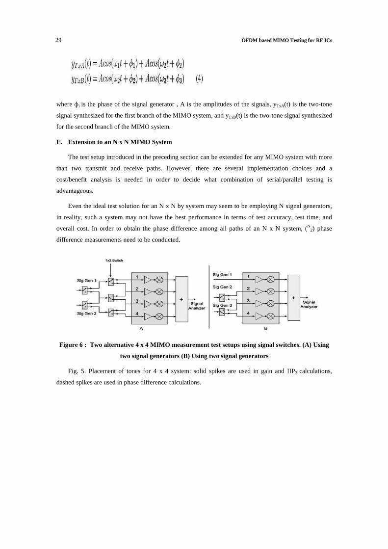
E. Extension to an N x N MIMO System
The test setup introduced in the preceding section can be extended for any MIMO system with more
than two transmit and receive paths. However, there are several implementation choices and a
cost/benefit analysis is needed in order to decide what combination of serial/parallel testing is
advantageous.
Even the ideal test solution for an N x N by system may seem to be employing N signal generators,
in reality, such a system may not have the best performance in terms of test accuracy, test time, and
overall cost. In order to obtain the phase difference among all paths of an N x N system, (N2) phase
difference measurements need to be conducted.
Figure 6 : Two alternative 4 x 4 MIMO measurement test setups using signal switches. (A) Using
two signal generators (B) Using two signal generators
Fig. 5. Placement of tones for 4 x 4 system: solid spikes are used in gain and IIP3 calculations,
dashed spikes are used in phase difference calculations.
Gopala Krishna.M, Eswara Rao.Y, Uma Sankar.Ch & Phani Kumar.Y 30
Fig. 5 shows a potential frequency domain multiplexing scheme for a 4 x 4 MIMO system.
Table I explains the purpose of the numbered frequency locations. This scheme requires only N
input tones for an N x N system to characterize the required performance parameters as opposed to 2(N-
1) tones.
A high number of spectral components for each path results in an increased number of inter-
modulation products. These tones clutter the spectrum and even overlap with information bearing
signals. This problem can be prevented through significantly reducing the power of the spectral
components used in phase measurements (tones 11–14 in Fig. 5). The power of intermodulation products
arising from these additional tones will be much smaller compared to the fundamental. This improves the
measurement accuracy.
However, using N signal generators to test an N x N system may be infeasible due to the need for a
high number of signal generators. Alternative test setups can be designed based on the number of
available signal generators and using signal switches.
For example, as shown in Fig. 6, two distinct test setups can be constructed for a 4 x 4 MIMO
system using switches.
The first measurement setup [shown in Fig. 6(a)] employs two signal generators and several signal
forwarding switches. By controlling the poles of the switches, the performance parameters of all paths
and their phase differences can be measured. The number of switching operations required for this case is
6 (1-2, 1-3, 1-4, 2-3, 2-4, 3-4).
OFDM based MIMO Testing for RF ICs 31
While the resulting number of switching is more than the number of switching that would be spent
using a sequential approach, the phase difference measurement can be attained without requiring a
coherent instrumentation. Therefore, using two instruments can be still beneficial in terms of the fixed-
capital cost of the test setup.
F. Coupling Measurements
As MIMO devices contain multiple radios operating at the same band, inevitably, there will be a
coupling between the RF branches. A severe coupling may distort the operation of the circuit. The
frequency domain multiplexing scheme described earlier can be slightly modified to measure the
coupling between branches of a MIMO device. However, since a signal combiner is used at the output of
the previously demonstrated test setup, the coupling between branches may not be measured as the origin
of each tone is untraceable. In order to measure the coupling between two RF branches, more than one
signal analyzers are needed.
The frequency domain multiplexing scheme can be slightly modified to measure the coupling
between two branches of a MIMO device, as shown in Fig. 7.
In this setup, there are two signal analyzers and two signal generators. The coupling terms will
appear in both outputs. Since the power of leakage terms usually a lot smaller compared to fundamental
terms, the amplitudes of the fundamental terms may not be degraded while some additional spectral
components appear at the outputs of the branches. Based on the power of these additional tones, the
amount of coupling between two branches of the device can be calculated.
IV. EXPERIMENTAL RESULTS
The test methodology is validated through simulations and measurements on a prototype MIMO
device. The goal in conducting the simulations is to demonstrate the robustness of this test methodology
Gopala Krishna.M, Eswara Rao.Y, Uma Sankar.Ch & Phani Kumar.Y 32
under process variations. In addition, the feasibility of this test methodology is demonstrated on a
prototype device, which consists of a MIMO transceiver built from off-the shelf integrated circuits, and
bench instruments for signal generation and analysis.
Figure 7 : Measurement setup for coupling between RF branches
Figure 8 : MIMO system model used in MATLAB simulations
A. Simulation Results
The block diagram of the MIMO transmitter that is used for simulations is illustrated in Fig. 8. The
transmit paths contain up-conversion mixers and power amplifiers (PA), which are modeled trough a
polynomial equation outlined below to emulate the nonlinear behaviors (Gain compression and IIP3), and
phase shift [15].
Where αi is the coefficient of the i th order term, ф is the injected phase, x(t) is the input signal, and
y(t) is the output signal. The gain and phase imbalances are injected through changing the polynomial
coefficients and the ф parameter.
The first case illustrates a circuit instance which has a very small phase mismatch between the RF
branches, and a matched gain and IIP3. Since our combiner subtracts the outputs of the branches, when
the phase mismatch is small, the amplitude of waveform at the w2 frequency location that is observed at
the output will be very low. In this case, 1o degree phase imbalance is injected between the paths to
determine the accuracy of the phase measurements.
OFDM based MIMO Testing for RF ICs 33
The remaining cases identify circuits with increasing mismatch parameters between the transmit
branches.
Table III depicts the maximum Gain, IIP3 and phase errors and standard deviations obtained in 50
simulations. The results indicate that the gain, IIP3, and the phase mismatch between the RF branches can
be accurately determined even if the mismatch parameters are very large. This enables the accurate
characterization of the target performance parameters for both marginal and grossly defective circuits.
While the robustness of the test methodology under process variations demonstrated only on a
transmitter, similar results can be obtained for a receiver, as demonstrated in the following section.
B. Measurement Results
In order to validate the theory, experiments are conducted on a MIMO device that is built using off-
the-shelf integrated circuits. Monolithic transmitter and receiver integrated circuits are used to build the
transceiver circuit. The baseband signal generators of Agilent E4438C signal generator are used to
generate low-frequency test signals and its RF frequency generator is employed to supply local oscillator
signals to the up and down-conversion mixers. In order to inject phase differences among RF
branches, different length cables are used to build a differential measurement system, which is illustrated
in Fig. 9. Cables with different lengths have different time delays, which eventually reflect as a phase
mismatch. Three different cable lengths are used: 1”, 18”, and 36” cables with time delays of 3 ps, 1.7 ns,
and 3.5 ns, which shift the phase of the signal at 6 MHz by 0.01, 3.7, and 7.6 degrees, respectively.
Figure 9 : Differential measurement system
Gopala Krishna.M, Eswara Rao.Y, Uma Sankar.Ch & Phani Kumar.Y 34
C. Extension to a 4 X 4 system
In this section, the simulation results are given for a 4x4 MIMO system using several test setups.
Table VI shows the measurement accuracies with respect to each test setup. Signal Generators shows the
number of signal generators used in each test setup, ADC Resolution shows the number of bits in each
signal generator, Gain Error shows the mean error in Gain measurements, IIP3 Error shows the mean
error in IIP3 measurements, and Phase Error shows the mean error in Phase measurements.
It can be observed that the measurement setup that uses only two signal generators is the most
accurate measurement setup. A detailed test cost-benefit analysis should be conducted in order to select
the best test setup [6].
V. CONCLUSIONS
A novel low cost MIMO test technique that enables measurement of critical performance
parameters, such as gain, IIP3, and the phase mismatch among the RF branches is presented. The test
methodology determines these parameters using a single test setup, thereby eliminating instrument
settling and switching times.
Based on our measurement results, the proposed method accurately determines the critical
performance parameters of the MIMO system while requiring only baseband signal generators, mixers,
and combiners.
The extensibility of the proposed method to any arbitrary MIMO configuration is also demonstrated
through simulations. Based on a cost-benefit analysis, the optimum test set can be determined using the
proposed test technique.
REFERENCES
1. Agilent Corp., USA, “Agilent 83236B PCS Interface Documentation,” 2006. [Online]. Available:
http://cp.literature.agilent.com/litweb/pdf/5965-5625E.pdf
2. Agilent Corp., USA, “MIMO Wireless LAN PHY Layer [RF] Operation and Measurement,” Appl.
Note 1509, 2005. [Online]. Available:http://cp.literature.agilent.com/litweb/pdf/5989-3443EN.pdf
OFDM based MIMO Testing for RF ICs 35
3. E. Acar and S. Ozev, “Efficient testing of RF MIMO transceivers used in WLAN applications,” in
Proc. IEEE Int. Conf. Comput. Des., 2006, pp. 432–437.
4. E. Acar, S. Ozev, and K. B. Redmond, “A low-cost RF MIMO test method using a single
measurement set-up,” in Proc. IEEE VLSI Test Symp., 2007, pp. 3–8.
5. H. Bolcskei, “MIMO-OFDM wireless systems: basics, Perspectives, and challenges,” IEEEWirel.
Commun., vol. 13, no. 4, pp. 31–37, Aug.2006.
6. S. Davidson, A. Ambler, and H. Davidson, “Behavioral test economics,” in Proc. IEEE Int. Test
Conf., A. Ambler, Ed., 2006, pp. 1–9.
7. R. Di Bari, M. Bard, Y. Zhang, K. M. Nasr, J. Cosmas, K. K. Loo, R.Nilavalan, H. Shirazi, and K.
Krishnapillai, “Laboratory measurement campaign of dvb-t signal with transmit delay diversity,”
IEEE Trans. Broadcasting, vol. 54, no. 3, pp. 532–541, Sep. 2008.
8. Barnes, J. Moreira, M. Comai, A. Islas, F. Tamayo-Broes, M. Resso, A.C. Scogna, O. Bell, and M.
Tsai, “Performance at the DUT: Techniques for evaluating the performance of an ATE system at the
device under test socket,” 2008. [Online].


![Hard Decision-Based PWM for MIMO-OFDM Radar · 2. MIMO-OFDM Radar Signal Model-Based PWM 2.1. MIMO-OFDM Radar Systems Structure In [1], OFDM technique has the advantage of combating](https://static.documents.pub/doc/80x56/5e6a685a5002aa073940e3bf/hard-decision-based-pwm-for-mimo-ofdm-radar-2-mimo-ofdm-radar-signal-model-based.jpg)


