2.5 Current Technology and Research.................................................................... 33 2.5.1 SDR and OFDM ........................................................................................ 33
2.6 Chapter Summary ............................................................................................. 36 Chapter 3: Proposed Research and Design..................................................................38
3.1 Design Requirements and Specifications: ........................................................ 38 3.1.1 System Requirements................................................................................. 39 3.1.2 Transmitter Specifications ......................................................................... 41 3.1.3 Receiver Specifications.............................................................................. 41
4.4.1 BER Performance in AWGN Channel ...................................................... 90 4.4.2 Simulated BER Performance with Timing and Frequency Offsets ........... 92 4.4.3 VHDL Implementation BER Performance................................................ 96 4.4.4 Laboratory Results: Example Transmission .............................................. 99
List of Figures: Figure 1.1: Spectrum measurement from 900 kHz to 1 GHz ............................................ 4 Figure 1.2: Four subcarrier OFDM spectrum .................................................................... 6 Figure 2.1: Illustration of an NC-OFDM system taking advantage of unused spectrum............................................................................................................................ 13 Figure 2.2: KUAR Hardware........................................................................................... 15 Figure 2.3: Spectrum and power spectral density of OFDM and FDM transmissions.... 18 Figure 2.4: Single carrier signal undergoing frequency selective fading ........................ 22 Figure 2.5: Approximately flat fading sub-channels in a frequency selective channel... 23 Figure 2.6: OFDM symbol with zero, 0.1, 0.25 and 0.5 sample period fractional timing offsets .................................................................................................................... 28 Figure 2.7: Inter-carrier interference caused by a frequency offset of 20% of a subcarrier spacing ............................................................................................................. 29 Figure 2.8: OFDM symbol with zero, 0.05, 0.1 and 0.25 subcarrier spacing fractional frequency offsets............................................................................................................... 31 Figure 2.9: Uncompensated 0.05 subcarrier spacing frequency offset over 5 consecutive data symbols.................................................................................................. 32 Figure 3.1: OFDM Transmitter Block Diagram .............................................................. 42 Figure 3.2: OFDM Receiver Block Diagram................................................................... 43 Figure 3.3: Illustration of the subcarrier assignments...................................................... 46 Figure 3.4: Base preamble sequence................................................................................ 47 Figure 3.5: Time domain representation of full preamble ............................................... 48 Figure 3.6: Kishore and Reddy algorithm operating in the absence of noise.................. 51 Figure 3.7: Kishore and Reddy algorithm operating at SNR = 10 dB............................. 51 Figure 3.8: Schmidl and Cox algorithm operating in the absence of noise ..................... 53 Figure 3.9: Schmidl and Cox algorithm operating at SNR = 10 dB................................ 53 Figure 3.10: Schmidl and Cox algorithm operating at SNR = 5 dB................................ 54 Figure 3.12: Residual carrier rotations to due integer timing frequency offsets with proposed channel estimation algorithm for offsets of 0, -2, -10, and -20 samples respectively ....................................................................................................................... 60 Figure 3.13: ISI due to integer timing offsets with proposed channel estimation algorithm for offsets of 0, 2, 5, and 10 samples respectively ........................................... 61 Figure 4.1: Receiver module port map ............................................................................ 66 Figure 4.2: External logic for top-level FPGA design..................................................... 67 Figure 4.3: Receiver module top level design ................................................................. 69 Figure 4.4: Inputs and outputs of the frame synchronization module ............................. 70 Figure 4.5: Implementation of Frame Synchronization Module ..................................... 70 Figure 4.6: Inputs and outputs of the fractional frequency estimation module ............... 72 Figure 4.7: Implementation of Fractional Frequency Estimation Module ...................... 72 Figure 4.8: Phase rotation module input and output ports............................................... 73 Figure 4.9: Phase rotation algorithm pseudo-code .......................................................... 74 Figure 4.10: Frequency offset compensation module inputs and outputs ....................... 75 Figure 4.11: Implementation of Fractional Frequency Compensation Module............... 76
ix
Figure 4.12: Port map of FFT module ............................................................................. 77 Figure 4.13: Implementation of FFT module .................................................................. 77 Figure 4.14: Port map of channel estimation................................................................... 78 Figure 4.15: Implementation of Channel Estimation and Equalization module.............. 79 Figure 4.16: CPE estimation and compensation module port map.................................. 81 Figure 4.17: VHDL implementation of CPE estimation and compensation module ...... 81 Figure 4.18: Carrier Demapping / QPSK Demodulation module port map .................... 83 Figure 4.19: VHDL implementation of Carrier Demapping / QPSK demodulation module............................................................................................................................... 83 Figure 4.20: Port Map of VHDL Transmitter.................................................................. 85 Figure 4.21: Top level FPGA design for OFDM transmitter .......................................... 85 Figure 4.22: Detailed design of OFDM transmitter......................................................... 87 Figure 4.23: Validation for BER of OFDM design in pure AWGN channel .................. 92 Figure 4.24: BER performance of Matlab simulations.................................................... 94 Figure 4.25: VHDL system versus Matlab simulation BER ........................................... 98 Figure 4.26: Received OFDM signal with no filtering.................................................. 100 Figure 4.27: Received OFDM signal with 8x interpolating filter.................................. 101 Figure 4.28: KUAR “across the room” laboratory transmission and reception of 1 frame including 7 OFDM data symbols. 2688 bits, BER = 0......................................... 102
x
List of Tables:
Table 3.1: Subcarrier index assignment........................................................................... 46 Table 4.1: Threshold values for each value of Eb/N0: Simulation ................................... 96 Table 4.2: Threshold values for each value of Eb/N0: VHDL.......................................... 98
xi
Chapter 1: Introduction
1.1 Research Motivation - Spectrum Scarcity
In the design of a communications system, there are essentially three factors that
limit the performance of a system: bandwidth, transmit power, and complexity. The
combination of these three factors determines how much data can be reliably
transmitted from one radio to another [1]. To some extent, one can be exchanged for
the other. A radio could employ more complex algorithms in order to conserve
transmit power and bandwidth, or it could transmit with a very high power level and
conserve bandwidth and complexity, and so on. However each of these three factors
is constrained by a practical limit. A cell-phone handset can only transmit so much
power safely, and they are limited by having a finite source of energy from the
battery. The complexity of a device is constrained by costs of research and
development, and the processing ability of modern semiconductor technology. These
limitations and tradeoffs of complexity and transmit power can differ from user to
user, but transmission bandwidth is the one commodity that all wireless users must
share. This is one of the reasons that bandwidth is by far the most precious
commodity in the current wireless industry.
There is a finite amount of bandwidth available for use. Although the electro-
magnetic spectrum theoretically is infinite in size, there is a sub-set of those
frequencies that are actually practical for wireless communications systems. The size
1
of the antenna for transmission and reception must be proportional to the wavelength
of the radio wave. This imposes limits on extremely low and extremely high
frequencies. In addition, as frequencies increase, the propagation loss increases and
the need for line-of-sight communication becomes more of an issue. Transmit
frequencies greater than 10 GHz are very difficult to operate without a line-of-sight
path from the transmitter to receiver [2]. Frequencies greater than 50 GHz begin to be
absorbed by oxygen in the atmosphere and may even become unusable in the
presence of rain [3]. Additionally, RF hardware becomes more expensive and
difficult to implement as frequencies increase.
Fortunately, bandwidth is reusable spatially – a key example being a network cell,
allowing two users to use the same spectrum, provided they spatially separated in two
different cells. Bandwidth is also reusable temporally, where different users can
operate in the same bandwidth, but not at the same time. Bandwidth can also be
shared among users in both time and frequency, such as with code division multiple
access (CDMA) systems, however, there is still a limit to the number of users who
can simultaneously use the same bandwidth.
The wireless communications industry is growing rapidly both in the number of
users and in the amount of bandwidth required by each user. Cellular technology is
advancing from voice communications, which requires relatively little bandwidth, to
data and video communications, which requires much more bandwidth. Wireless
internet access is evolving from WiFi systems, which have ranges of tens of meters,
to WiMAX systems which have ranges measured in kilometers. The increase in data
2
rate and range both require the consumption of bandwidth resources. These two
competing forces – the finite amount of available bandwidth and the increasing
demand for bandwidth – are exacerbated by the way in which spectrum is allocated to
consumers.
Radio spectrum is a natural resource. In the United States, the Federal
Communications Commission (FCC) is responsible for allocating this resource in
what is known as a “command-and-control” regulatory structure. In this system, the
spectrum is divided into frequency bands and allocate to various entities, such as
wireless service providers, which have exclusive rights to its use. As a result, there is
very little spectrum for unlicensed used.
When the initial spectrum allocations were made, radio technology was much
more primitive relative to today’s standards and the concept of users sharing the same
spectrum and geographic location was probably considered impractical. Moreover,
very strict rules prevented anyone other than the license holder from using this
spectrum. Unfortunately, numerous spectrum surveys show that much of the licensed
spectrum is severely underutilized [4]. Figure 1.1 depicts a spectrum measurement
performed in the 900 kHz to 1 GHz band. Since much of this band is television
stations, there is very little change in the spectrum over time. Note how there are
large gaps of unused spectrum in the figure. If these white spaces could be used by a
secondary unlicensed user, it would open up a large reservoir of unused spectrum that
could help accommodate the growing demand for additional bandwidth. The ability
3
for secondary (unlicensed), users to efficiently and intelligently exploit this unused
bandwidth is known as dynamic spectrum access (DSA).
Figure 1.1: Spectrum measurement from 900 kHz to 1 GHz [5]
1.2 Cognitive and Software-Defined Radios
One solution to the spectrum scarcity issue is the implementation of radios that
can automatically perform dynamic spectrum access with little or no assistance from
the user. A radio that can perform this task is known as a frequency agile radio,
which falls under the broader category of a cognitive radio [6]. An agile radio must
be able to sense its spectral surroundings and classify frequency bands as either signal
or noise [5]. Thus, any band classified as being only noise can then be exploited.
A cognitive radio would have all the properties of an agile radio plus the ability to
reconfigure itself for different applications and to adapt to the constraints placed by
the user. The cognitive radio would automatically adapt to the environment and user
constraints in an intelligent or cognitive manner by changing transmit power, center
frequency, coding rate, and other tunable parameters to meet user requirements
4
regarding error robustness, bandwidth requirements, and transmit power restrictions.
The reconfiguration process would involve changing basic system components, such
as the modulation or error control coding.
The reconfigurability and adaptability aspects of a cognitive radio necessitate a
software, rather than pure hardware, platform. The platform commonly used to
implement a cognitive radio is known as software-defined radio (SDR). A software-
defined radio performs all baseband operations and sometimes intermediate-
frequency (IF) operations entirely in software and/or in reconfigurable hardware such
as a field-programmable gate array (FPGA).
The University of Kansas has a software defined radio platform, known as the
Kansas University Agile Radio (KUAR), which is equally capable of implementing
radio components in software or in reconfigurable hardware. Work is currently in
progress to test advanced modulation schemes that are applicable to dynamic
spectrum access, as well as artificial intelligence algorithms that will eventually make
the KUAR a full cognitive radio platform. The work conducted in this thesis applies
to the modulation schemes.
1.3 Orthogonal Frequency Division Multiplexing
The primary goal of this thesis is the implementation of a high data-rate
modulation scheme on the KUAR that is capable of supporting dynamic spectrum
access communications. This modulation scheme is known as orthogonal frequency
division multiplexing (OFDM) [7]. OFDM is a multi-carrier modulation technique
that is spectrally efficient, extremely robust to harsh wireless channel environments,
5
and is well-suited to selectively populate areas of spectrum to avoid interfering with
primary users [8]. When broadcasting across a specific bandwidth, OFDM subcarriers
can be selectively disabled to prevent interfering with other users. This technique is
known as non-contiguous orthogonal frequency multiplexing (NC-OFDM) [9]. The
spectrum of a four subcarrier OFDM system is shown in Figure 1.2. Note how the
subcarriers overlap, yet are completely orthogonal, i.e. zero interference, at the peak
amplitude of each subcarrier.
Figure 1.2: Four subcarrier OFDM spectrum
1.4 Research Objectives and Contributions
The objective of this thesis is to implement an OFDM reference design based on
the IEEE 802.16-2004 OFDM PHY standard on the KUAR. The IEEE 802.16
6
standard is a specification for technology known more generally as WiMAX
(Worldwide Interoperability for Microwave Access). IEEE 802.16-2004 employs
OFDM transmission in what is currently the most advanced standard for fixed
wireless access. Note that although IEEE 802.16e is more recent than IEEE 802.16-
2004, it is designed to support mobile systems, and thus is outside the scope of this
thesis since the KUAR is not designed to be mobile during radio operation. Rather,
the KUAR units were designed to be nomadic, such that the radio is portable and can
be moved from location to location but it does not operate during movement.
Utilizing 256 subcarriers, the IEEE 802.16-2004 standard is higher performance
than previous generations of systems, such as the IEEE 802.11 WiFi family, which
utilized 64 subcarriers. In general, as data-rates increase, the number of subcarriers
must also increase to preserve the characteristics of OFDM in terms of its ability to
cope with distortion introduced by a wireless channel. Therefore, this standard
represents the benchmark by which all other stationary OFDM systems will be
compared. Moreover, the OFDM implementation in this thesis demonstrates the
processing ability of the KUAR, as well as serves as framework for NC-OFDM
system development. The main objectives of this thesis are as follows:
• Research, design, and validate in Matlab simulations, the algorithms that are
necessary for transmission across a wireless channel and that are applicable
for the structure of the IEEE 802.16-2004 standard. These include:
o Frame synchronization
o Frequency offset estimation and compensation
7
o Channel estimation and equalization
o Pilot carrier phase tracking and compensation
• Implement an OFDM transmitter and receiver on the KUAR and verify that it
can transmit reliably in a stationary, indoor environment.
• Validate the bit-error rate (BER) of the simulated OFDM system in an
AWGN channel, and then empirically evaluate the BER performance of the
implemented VHDL system.
The contributions of this thesis are as follows:
• The first known IEEE 802.16-2004 based OFDM design for a FPGA-based
software-defined radio that has actually been tested across an air medium with
RF hardware. There are many other IEEE 802.16-based FPGA designs, some
even implementing the entire standard [10], but none have yet been tested
with actual RF transmission and reception.
• Contributes a significant amount of design experience with the KUAR, Xilinx
tools, and design verification that is documented to serve as a framework
towards further development of the KUAR project.
• Establishes a hardware testbed foundation for advanced modulation schemes
employed in DSA networks.
8
1.5 Thesis Outline
The remainder of this thesis is organized as follows:
In chapter 2, background material on dynamic spectrum access, cognitive radios,
and the KUAR is presented. Following this is an overview of OFDM is presented,
covering the mathematical background, specific OFDM issues, and an explanation of
the challenges in timing and synchronization. The last section of the chapter covers a
brief analysis other similar work in cognitive radio, software defined radio, and any
OFDM systems implemented on these radios.
In chapter 3, the proposed research and design necessary to eventually implement
the reference design in VHDL is discussed. Design constraints and goals are outlined,
followed by block diagrams of the top level design. The mathematical description of
how each block should operate is then considered, with special attention given to the
synchronization algorithms, which are then outlined including how they are designed
around the IEEE 802.16-2004 OFDM preamble. Throughout this chapter, examples
are supplied from the Matlab simulations to aid in the explanation.
In chapter 4, details of the actual implementation outlined in chapter 3 are
covered. This includes a top level design of the transmitter and receiver in terms of
the VHDL modules, followed by a detailed description of the IP cores and processes
that implement each of these modules. Chapter 4 concludes by comparing the bit-
error rate of the Matlab simulations with the actual VHDL implementation.
9
In chapter 5, concluding remarks reached from the implementation and validation
processes presented in chapter 4 are made. Several ideas and direction for future work
are also outlined.
10
Chapter 2: Background Literature
2.1 Dynamic Spectrum Access
As briefly introduced in Chapter 1, DSA is one approach to alleviating the
spectrum scarcity problem. Comprehensive measurements [4] and analysis of
spectrum data throughout the United States [11] have shown that large amounts of
spectrum is unused and could be exploited by secondary users, particularly in the TV
bands (approximately 50-700 MHz). It should be noted that DSA is not currently
permitted, as the FCC does not allow secondary users in licensed spectrum.
Nevertheless, this is expected to change as the FCC continues investigate this
approach [12].
While relatively straightforward in concept, there are a number of challenges in
implementing practical DSA systems. The band in which the radio wishes to transmit
in must be carefully examined before transmission to ensure that there is no
interference with the primary user. However, there are many different types of
signals, and detecting them requires different algorithms. For instance, spread
spectrum or ultra wide-band signals would be particularly difficult to detect and
measure, especially compared to signals such as a FM radio or TV station that have
well-pronounced spectral properties. Additionally, primary users may vary their
spectrum usage significantly with time. Some users may only transmit bursts of data
at statistically random intervals, while others may transmit continuously. Obviously,
11
many characteristics of the primary users must be measured and accounted for before
employing DSA.
Another challenge with DSA is assessing the viability of a particular band of
spectrum. Some unoccupied bands of spectrum may have poor propagation and
multipath characteristics, making them nearly unusable. One method of assessing the
channel conditions is to use a channel sounder, such as a swept time delay cross-
correlator (STDCC). However, if wideband channel sounding is employed within a
bandwidth occupied by primary users, this presents another interference problem.
One solution to this is the use of a spread spectrum channel sounder, where the degree
of spreading is dictated by the primary user’s tolerance to interference [13].
Another important issue is the need to accomplish wideband communications in
the DSA context within a band of spectrum populated by narrow-band primary users.
One approach would be to use a standard spread spectrum technique, but this would
inevitably raise the noise-floor, affecting the primary user’s communications. Another
proposed technique, known as spectrum pooling [8], would use a wide-band OFDM
signal with specific subcarriers disabled in order to prevent interference with the
primary user. This technique is also known as non-contiguous orthogonal frequency
division multiplexing (NC-OFDM) [9]. This technique enables one radio to transmit
over multiple, non-contiguous frequency bands all in one channel. This concept,
complimented with ability to mitigate the effects of harsh multipath channel
environments, makes NC-OFDM a very important modulation scheme for agile and
12
cognitive radios. An illustration of the concept of spectrum pooling and NC-OFDM is
provided in Figure 2.1.
Figure 2.1: Illustration of an NC-OFDM system taking advantage of unused spectrum [14]
2.2 Cognitive radios
A cognitive radio is a wireless communications device that can change both its
own parameters to maximize performance given user constraints, as well as perform
DSA in order to avoid interference with licensed users and other unlicensed users. A
cognitive radio would be able to adapt its parameters, such as transmit power, coding
rating, frame size, bandwidth, and center frequency, in real time to maximize
performance in a given environment. The radio would also be reconfigurable in order
to conform to any wireless standard. The cognitive radio could, with equal ability,
transmit and receiver AM radio, WiFi, WiMAX, GSM, WCDMA, and other well-
defined access schemes.
In order to adapt to the channel conditions and user constraints efficiently without
user guidance, the radio must have some capacity of artificial intelligence. Several
13
methods for artificial intelligence employed by cognitive radios include expert or
knowledge based systems, neutral networks, and genetic algorithms [15]. Knowledge-
based reasoning systems are simple to implement, but require large amounts of
memory storage and are not capable of adapting to unique situations. Neural networks
are a promising solution in that they are highly adaptable and need little storage
space. They analyze information in a highly parallel way, loosely modeled after the
human brain. However, neural networks can be extremely unpredictable, and the
reasoning they use to arrive at a solution can be very difficult to ascertain, making
debugging a very undesirable prospect. Genetic algorithms are good at finding near
optimal solutions when the problem has many degrees of freedom, making an
analytical solution impossible and a knowledge-based system impractical.
Within the cognitive radio research community, genetic algorithms have been
receiving a significant amount of attention [15], [16]. A genetic algorithm would
control a cognitive radio as follows: First a fitness function must be defined, which
scores each solution provided. The fitness function would consist of a set of
objectives that are important to the user, such as minimize BER, maximize data rate,
minimize power consumption, or any other quantitative measure of performance. The
user could determine the importance of each objective by assigning a weight to it,
which would be accounted for in the fitness function. The algorithm would then begin
generating a fixed number of random solutions and scoring each via the fitness
function. Solutions that provided the highest scores would then be combined with
each other by swapping or averaging parameters between pairs and discarding the
14
solutions that scored the poorest. Additionally, random mutations would be added by
randomly adjusting parameters in each generation to prevent the solutions from
converging to local maxima.
2.3 Kansas University Agile Radio
The KUAR is a software-defined radio developed at the Information and
Telecommunication Technology Center (ITTC) at the University of Kansas [17]. It is
designed as an experimental platform for research in wireless radio networks,
cognitive radios, and dynamic spectrum access. As seen in Figure 2.2, the KUAR
composed of three separate printed circuit boards: the digital signal processing board,
power supply board, and RF board.
Figure 2.2: KUAR Hardware [17]
The digital signal processing board features a PC composed of a 1.4 GHz Pentium
M processor, 1 GB DDR2 SDRAM, and an 8 GB MicroDisk for data storage. This
15
processor connects to the digital board itself via a PCI Express bus. The PC uses
Linux for the operating system and features a VGA, USB 2.0, PCI Express, and
Gigabit Ethernet (10/100/1000 Mbps). The large processing resources allow the
KUAR to be used as a genuine software-defined radio.
In addition to the processing resources, the KUAR features a Xilinx Virtex II Pro,
a field-programmable gate array (FPGA), which can be employed to program radio
components in hardware. Hardware implementations of radio components have the
ability to take advantage of performing operations in parallel. This is particularly
advantageous to OFDM systems, which require Fast Fourier Transform (FFT)
operations. A FFT implemented in the FPGA will execute far more quickly than if it
were implemented in software, allowing much higher data rates.
All radio components so far implemented in the KUAR have been exclusively
accomplished using the FPGA. The addition of the high performance PC has been a
recent addition which will allow for combination hardware/software designs or for
entirely software designs. Despite the advantages of hardware or hardware/software
designs, most current software-defined radio research is done in pure software, such
as the case with the GNU Radio software, which the KUAR is designed to support.
The RF board is designed to operate in the frequency range of 5.25-5.85 GHz,
selecting 30 MHz sections of bandwidth. This frequency range was selected for
compatibility with the Unlicensed National Information Infrastructure (UNII) and
Industrial, Scientific, and Medical bands. The digital signal processing board
interfaces with the RF board through a dual 16-bit Digital to Analog Converter
16
(DAC) and two 14-bit Analog to Digital Converters (ADC). The DAC converts the I
and Q channels separately into analog signals, which are then passed to a quadrature
modulator which combines them into a real signal. On the receive side the I and Q
channels are digitized separately by the two ADCs.
This is one advantage built into the KUAR – the FPGA isn’t burdened by any
down-conversion from IF frequencies, freeing the logic resources to be devoted
entirely to baseband processing. This also helps separate baseband and RF
functionality, so that baseband radio designs can, which the exception of receiver
filtering, ignore the RF functionality.
The reader is encouraged to read reference [17] for a more detailed description of
the KUAR.
2.3 OFDM Overview
2.3.1 What is OFDM?
OFDM is a digital modulation scheme that is used in both wireline and wireless
systems to transmit numerous modulated carriers that are mathematically orthogonal
to each other. In other words, the subcarriers ideally exhibit zero mutual inference.
OFDM is similar to frequency division multiplexing (FDM) in that it multiplexes
carriers across frequency, but with two important differences. First, FDM is the
traditional method to separate signals intended for different radios. When it is used to
allow multiple users to share the same channel it is called frequency-division multiple
access (FDMA). OFDM is often used for multiple access as well, but the primary
17
motivation for using OFDM is to increase performance over using a single carrier
modulation. Secondly, OFDM differs from traditional FDM in its subcarrier spacing.
In OFDM, the carriers overlap to a great degree, as previously shown in Figure 1.2.
Each carrier is ideally represented mathematically by a sin(x)/x pulse, which have
nulls at a spacing of 1/Ts where Ts is the symbol time of each subcarrier. In OFDM,
the carrier spacing is 1/Ts, which is precisely the location of nulls in a sin(x)/x pulse
and thus, ideally, there is zero inter-carrier interference (ICI). This is a secondary
advantage of OFDM, in that it is more spectrally efficient than standard FDM. The
spectrum and power spectral density of OFDM and FDM are contrasted in Figure 2.3.
Figure 2.3: Spectrum and power spectral density of OFDM and FDM transmissions
18
2.3.2 Mathematical Representation
At baseband, an OFDM signal can be represented by a sum of modulated complex
exponentials,
( ftkjXtSN
kk Δ= ∑
−
=
π2exp)(1
0
)
)
(2.1)
where Xk is a complex number representing a BPSK, QPSK, or QAM baseband
symbol modulating the kth subcarrier and Δf is the subcarrier spacing. If this signal is
sampled as in Equation (2.2),
( s
N
kks fnTkjXnTS Δ= ∑
−
=
π2exp)(1
0 (2.2)
then the sampled signal is exactly equivalent to an inverse N-point discrete Fourier
transform (DFT), taking the Xk as the frequency bin arguments [18]. The DFT and
the inverse DFT are given in Equations (2.3) and (2.4).
1,...,02exp1
0−=⎟
⎠⎞
⎜⎝⎛ −= ∑
−
=
NlN
lnjxXN
lnl
π (2.3)
1,...,02exp1 1
0−=⎟
⎠⎞
⎜⎝⎛= ∑
−
=
NnN
lnjXN
xN
nln
π (2.4)
The Fast Fourier Transform (FFT) is simply a computationally efficient
implementation of the DFT. The IFFT and FFT are the core modulation and
demodulation operations used in OFDM.
19
2.3.3 OFDM versus Single Carrier Modulation
Wireless communications systems at the physical layer level must deal with a
potentially hostile channel environment. Among these are additive white Gaussian
noise (AWGN), multi-path propagation, large-scale fading and shadowing, non-linear
interference introduced by amplifiers and filters, and analog-to-digital conversion. By
far the most serious of these corruptions is multipath propagation, where the radio
signal arrives at the receiver via two or more paths. Understanding the wireless
channel and multipath propagation is crucial in the justification of using OFDM.
The phenomenon of multiple signal paths arriving and interfering at the antenna is
generally known as small-scale fading [19]. This is opposed to large-scale fading,
which occurs when large obtrusive objects (or simply large distances between radios)
drastically reduce received signal power [19]. Large scale fading is typically
compensated for by varying the transmit power accordingly. Small-scale fading can
be broken down into roughly two concepts: (i) fading due to Doppler spread, and (ii)
fading due to multi-path delay spread. The effect of the multipath channel can be
fully characterized by Equation (2.5), where y is the received signal, x is the
transmitted signal, and h is the channel transfer function [19].
),()()( tdhtxty ⊗= (2.5)
The channel impulse response varies both as a function of delay, d, and time, t. Signal
paths will arrive at the antenna at different delays and the magnitude and phase of
these paths will change over time.
20
Doppler spread refers to the dispersion in frequency caused by the motion of one
or both radios while communicating with each other. The motion of the radios causes
a Doppler shift, the degree of which can be characterized by a Doppler bandwidth.
The greater the Doppler bandwidth, the greater the variations of h(d, t) with time.
Fading due to multi-path delay spread is due to different paths arriving at different
times at the antenna. If all the significant paths (in terms of power) arrive within the
time of a single symbol period, the net effect is a random complex attenuation of the
symbol. This type of distortion is known as flat fading. If the significant paths arrive
at time intervals greater than a symbol period, in addition to the random complex
attenuation, there is inter-symbol interference (ISI) in the time domain. Each path
effectively acts as a tap in an FIR filter, which smears the signal in the time domain
and filters it in the frequency domain. This is known as frequency selective fading.
ISI and frequency-selective fading are the crucial bottlenecks for very high data-
rate systems using single carrier modulation. It can be compensated for using
complex adaptive multi-tap equalizers and error control coding, but there comes a
certain point at which the cost of combating ISI and frequency-selective fading
outweigh the benefits of using a single-carrier modulation technique. An OFDM
system can alleviate the ISI and frequency selective fading problem without the need
for complex equalization.
The primary advantage of OFDM is that by using multiple distinct subcarriers, a
frequency selective fading channel can be transformed into multiple approximately
flat-fading channels. This principle is best understood graphically by Figures 2.4 and
21
2.5. In each figure, the transmitted signal is filtered by the transfer function of
channel, leading to distortion of the signal. Clearly, the distortion imparted to the
OFDM signal is much less severe.
Figure 2.4: Single carrier signal undergoing frequency selective fading
22
Figure 2.5: Approximately flat fading sub-channels in a frequency selective channel
Figure 2.4 demonstrates a situation where the channel frequency response due to
multi-path is varying in frequency more quickly than the signal is. The bandwidth
over which the magnitude response of the channel is basically flat is known as the
coherence bandwidth. Obviously, the bandwidth of the signal in Figure 2.4 is greater
than the coherence bandwidth of the channel. Conversely, in the OFDM signal in
Figure 2.5, each subcarrier has a bandwidth smaller than the coherence bandwidth of
the channel. If the bandwidth of each signal passing over the channel is smaller than
the coherence bandwidth, the signal will undergo flat fading.
When designing an OFDM system, the individual subcarrier bandwidth is set to
be significantly smaller than the coherence bandwidth. OFDM is essentially a
23
solution to severe frequency-selective fading, which is one of the most significant
challenges for single-carrier systems attempting to achieve higher data rates.
2.3.4 Guard Interval & Cyclic Prefix
Although a properly designed OFDM system will exhibit flat-fading (and thus no
ISI) in each sub-channel, the OFDM symbols as a whole are still vulnerable to ISI. In
an OFDM system, ISI causes severe interference that is difficult to recover from.
Therefore, the issue is usually avoided entirely by inserting a guard interval between
OFDM symbols in the time domain that is designed to be longer than the maximum
delay spread of the channel, thus eliminating the possibility of ISI. However, there is
a trade off between the guard interval and the data throughput.
The most common form of guard interval is a cyclic prefix, where a certain
number of samples at the end of the time-domain OFDM symbol are copied to the
beginning. The cyclic prefix is used in a variety of ways in different OFDM system
implementations, including timing synchronization, frequency synchronization, and
carrier equalization. Another benefit of the cyclic prefix is that if the FFT is
windowed earlier than the optimal sampling time, it will still “catch” all of the
required samples and symbol energy to reproduce the original frequency domain
symbols without ISI.
2.3.5 Peak-to-Average Power Problem
Single carrier systems using BPSK, QPSK, or QAM have known envelope
signals, and thus known output power levels as well. Conversely, OFDM is a sum of
24
modulated subcarriers and therefore can exhibit a widely varying signal envelope.
The maximum peak-to-average power ratio (PAPR) of an OFDM system is
approximately equal to the number of subcarriers, N [20]. This large variation in
signal power has two possible consequences. During the actual IFFT and FFT
calculations, the output of the transform requires more bits to represent the sample
than those of the input samples. If these output samples are truncated to the same
number of bits as the input samples, there is a loss of precision which leads to a
degradation in the signal-to-noise ratio. The second more commonly referenced
problem is that the RF amplifiers used to transmit the OFDM signal must either have
really large dynamic range, or must be operated with a large back-off, which will also
lead to a degradation of the signal-to-noise ratio.
PAPR reduction is not investigated nor implemented in this thesis, but it is a very
important characteristic to keep in mind when considering the merits of OFDM. If
low-cost non-linear amplifiers are the only RF equipment available for a given
design, one must reconsider choosing OFDM transmission, regardless of the benefit
from combating frequency-selective fading.
2.4 Synchronization Issues
Synchronization is a critical task for any radio receiver and is sometimes over-
looked in academic discussions of communication systems. However, since this thesis
is based around building an OFDM system in hardware, the synchronization problem
is not only relevant but, it is the most important issue. There are two primary
problems in synchronization – sample clock timing offsets and carrier frequency
25
offsets. Additionally, there are issues introduced from clock jitter and phase noise
which can manifest itself as common phase error (CPE), a random rotation of the
entire signal constellation that must be accounted for and compensated as well.
2.4.1 Timing Offsets
The term timing offset refers to differences in ideal sampling time for a received
signal and the actual sampling time for a transmitted symbol. In a single carrier
system, the receiver tries to correct for timing offsets by attempting to recover the
transmitter’s symbol clock. Once the receiver acquires an estimate of the symbol
clock, it can either realign its own symbol timing clock using a phase-lock loop
(PLL) or it can use an interpolator to estimate the received symbol without correcting
the symbol clock offset.
In OFDM, timing offsets can be divided into two categories: fractional and
integer. Fractional offsets refer to a phase offset in the sampling clock of the analog-
to-digital converter (ADC) of the receiver as compared to the phase of the transmitted
signal. Integer offsets refer to offsets greater than one sample period, which cause the
FFT window to be misaligned. If the FFT is taken early, some of the cyclic prefix
samples from the current symbol are used to calculate the FFT. If the FFT is taken too
late, part of the cyclic prefix of the following symbol is used, leading to ISI.
Neglecting any possible ISI, both integer and fractional timing offsets manifest as
sub-carrier rotation. This carrier rotation is easily conceptualized by the following
Fourier Transform property:
26
( ) ( ) ( )ωωτ Ftjtf −↔− exp (2.6)
Equation (2.6) describes how a time delay in the time domain implies a phase
rotation in the frequency domain. Also, the degree of the phase shift is determined by
the expression –jωt, meaning that the phase shift is proportional to both the time
delay and the frequency component being rotated. Therefore, in an OFDM signal, the
timing offsets manifest as progressive subcarrier rotations, where the further the
carrier is from the DC, the more the subcarrier is rotated. Equation (2.7) describes
how the carriers are rotated, where n is the carrier index, N is the total number of
carriers, and C is the carrier prior to rotation, RC is the rotated carrier, and Δt is the
timing offset in samples (both integer and fractional).
⎟⎠⎞
⎜⎝⎛ Δ−
=N
tnjCRC nnπ2exp n = (-N/2), …., N/2 - 1 (2.7)
Also note that a baseband OFDM signal has carriers from –N/2 to N/2 - 1. For
example, a 256 subcarrier OFDM signal has carriers indexed from -128 to +127,
including a 0 index “DC” carrier.
Carrier rotations are also caused by multipath channels such that the two effects,
fading and timing offsets, are indistinguishable at the receiver. Therefore, the two
corruptions are both handled by a channel estimator. The plots below in Figure 2.6
demonstrate the effects of uncompensated timing offsets on a single 256 subcarrier
OFDM symbol utilizing QPSK subcarriers. Each plot depicts a constellation diagram
for one 256 subcarrier OFDM symbol using QPSK subcarrier modulation for various
fractional timing offsets in a noiseless system.
27
Figure 2.6: OFDM symbol with zero, 0.1, 0.25 and 0.5 sample period fractional timing offsets
As can be seen, the effects of timing offsets are quite catastrophic, so BER plots
are not very informative. Implementation of the channel estimation algorithm used to
correct timing offsets is discussed further in Chapter 3.
2.4.2 Frequency Offsets
The term frequency offset refers to a non-zero carrier frequency seen at baseband
in the receiver. Carrier offsets are caused by imperfect demodulation from RF, as well
as frequency drift caused by Doppler shift. Both of these cause the OFDM subcarriers
to be viewed at the receiver as slightly different frequencies than intended and must
be compensated for in order to avoid either inter-carrier interference or having
28
subcarriers end up in the completely wrong frequency bin post-FFT. OFDM is
extremely sensitive to frequency offsets, given the highly dense spectral
characteristics of OFDM. Since the carriers are overlapping on each other, small
frequency offsets cause large amounts of interference. This is depicted in Figure 2.7.
With no frequency offsets, an FFT applied to the signal below will sample the value
at the peak of each x
x)sin( pulse. However, with a frequency offset, each frequency
bin of the FFT will capture energy from many of the carriers added together. Each
square marker in Figure 2.7 represents a contribution of ICI.
Figure 2.7: Inter-carrier interference caused by a frequency offset of 20% of a
subcarrier spacing
As can be seen, the adjacent subcarrier introduces an interference component that
is about half the amplitude of the subcarrier of interest. All other subcarriers introduce
29
an interference component of much lower amplitude. This is known as a loss of
orthogonality, and must be compensated for in order to properly demodulate the
OFDM symbol.
The effect of frequency offsets in the time domain can easily be understood by
taking the Fourier transform pair from Equation (2.6), which is repeated here for
convenience:
( ) ( ) ( )ωωτ Ftjtf −↔− exp
By swapping the frequency and time domains, it can be shown that a shift in
frequency causes an evolving phase shift in the time domain. The time domain
samples are rotated according to Equation (2.8),
( ) ( )NfnjnSnS /2exp)(' Δ−= π (2.8)
where S’ are the rotated samples, S are the original samples, n is the sample index, Δf
is the frequency offset in subcarrier spacings, and N is the number of subcarriers. The
effects of uncompensated frequency offsets are demonstrated in Figure 2.8. Each plot
depicts one 256 sub-carrier OFDM symbol using QPSK subcarrier modulation for
various frequency offsets in a noiseless system.
30
Figure 2.8: OFDM symbol with zero, 0.05, 0.1 and 0.25 subcarrier spacing fractional
frequency offsets
As can be seen, OFDM is quite sensitive to even small frequency offsets. Small
offsets cause dispersion in the constellation points similar to AWGN, but also cause a
general rotation in the constellation points. If there are multiple data symbols in the
packet, even this small offset will cause constellation points to drift over the decision
boundaries, as can be seen in Figure 2.9 below.
31
Figure 2.9: Uncompensated 0.05 subcarrier spacing frequency offset over 5 consecutive data symbols
In the presence of noise, an actual system will not perfectly measure frequency
offsets, so there will inevitably be some small residual frequency offset, such as in
Figure 2.9. The constellation rotation caused by residual frequency errors is usually
indistinguishable from constellation rotation caused by phase noise, which is
discussed in the next section. Correcting constellation rotation is usually done with
pilot carriers, which is covered in Chapter 3.
2.4.3 Phase Noise
Phase noise is introduced by imperfections in the local oscillators or by clock
jitter in the sampling clock. In either case, phase noise manifests as two different
phenomenon: common phase error and inter-carrier interference [21]. The overall
effect is determined by the bandwidth of the phase noise is relation to the bandwidth
of the OFDM system. If the phase noise is changing significantly faster than the
32
duration of an OFDM symbol, there will be loss of orthogonality, and thus, inter-
carrier interference. However, if the phase is changing more slowly than the duration
of the OFDM symbol, there will be a constant phase term added to each sample. This
will result in common carrier error (CPE) [21] – each carrier in the OFDM symbol
will be rotated by the same amount. However, unlike the effects of timing errors,
there will be a different constant carrier rotation for each OFDM symbol. This is
similar to the effect of residual frequency offsets, covered in the previous section. As
stated previously, the constellation rotations are typically corrected for using pilot
carriers that are embedded in each data symbol. The implementation of this is
discussed in Chapters 3 and 4.
2.5 Current Technology and Research
This section is designed to provide the reader with brief overview of the current
research into SDR-based OFDM systems. The following is not an exhaustive list of
all current research, but it should give the reader some insight into how the KUAR
and this thesis fit into the current research community.
2.5.1 SDR and OFDM GNU Radio
The most ubiquitous SDR is GNU radio, which is a free software toolkit.
Although there are no known OFDM implementations using GNU radio, it still bears
mention being the mostly commonly known SDR platform. GNU radio isn’t intended
for any one particular hardware platform, but it is often used with the Universal
33
Software Radio Peripheral (USRP), built by the GNU radio project. The USRP
includes four DACs and four ADCs and a USB interface. It supports RF
daughterboard add-ons for various frequency bands. The USRP has an imbedded
FPGA, but it is not used for radio components. Rather, it is used for digital up-
conversion and down-conversion. GNU radio is intended to be an entirely software
based system that does the baseband processing on a PC and then uses a separate RF
front-end.
Trinity College Dublin
The Networks and Telecommunications Research Group (NTRG) at Trinity
College focuses on implementations of software radios on general purpose processors
(PCs) [22]. Their SDR platform consists of a receiver and transmitter consist of
minimal RF front end, IF amplifiers, A/D and D/A cards, and a PC [23]. They have
developed an XML based software tool called IRIS (Implementing Radio is
Software) that they have used to build an OFDM system on their SDR platform [24].
They are also investigating “dynamically reconfigurable radios” [23], which seem to
implement some of the key functionality of cognitive radios without emphasizing the
actual AI cognition.
University of Laval
Sebastian Roy and Paul Fortier from the University of Laval have implemented an
FPGA implementation of an uncoded OFDM transmitter and receiver with a feedback
link [25]. Their design uses different QAM modulation constellation depending on
the current channel conditions. The receiver can automatically determine which
34
constellation is currently being transmitted. Synchronization between the transmitter
and receiver is assumed, as the research is more concerned with adaptive modulation.
The system is implemented in a Virtex II XC2V6000 and tested at baseband with a
wireless channel model to validate the design
INAOE Puebla, Mexico
Joaquin Garcia and Rene Cumplido have published several papers including [26]
and [27] on the implementation of 802.11a and 802.16-2004 modulators implemented
in an FPGA. A key emphasis of their work is using Xilinx System Generator for very
high level abstract design.
Lattice Semiconductor UK Ltd.
Lattice Semiconductor has fully implemented the 802.16-2004 standard in an
OFDM transceiver on a Lattice ECP33 FPGA [28]. The system has been validated
using a Matlab program to generate test data that accounts for quantization effects,
timing and frequency offsets, SUI (Stanford University Intermim) model multipath,
phase noise, and AWGN. It has been vetted for receiver sensitivity tests and
minimum BER required for full 802.16-2004 validation. It is not clear from the
available literature whether it has been tested in a full SDR system. They have
produced several white papers including [29] that investigate synchronization issues.
The design presented in [29] evidently uses a slightly more advanced version of the
Schmidl and Cox algorithm [30] used in this thesis. They also present alternate
algorithms that should be reviewed for future work.
35
IMEC
IMEC is an exclusively R&D company in Belgium that research includes
everything from nanotechnology to wireless communications to solar cells. In [31]
they presented an FPGA based OFDM design. Their OFDM design is based on a
previous ASIC (Application Specific Integrated Circuit) design they built to conform
to the IEEE 802.11a standard. Their design implemented in a Xilinx Virtex II
XC2V6000 FPGA (which has considerably more logic resources than the Virtex II
used in the KUAR: 33,792 logic slices compared to 9,280) and is capable of the full
20 MHz bandwidth and 72 Mbps data rate specified in the standard. The VHDL code
was generated from a dataflow model in C++ using software that is normally used for
generating ASIC designs.
IAF
IAF is a German company that specializes in cutting-edge wireless
communications technology. They have built several FPGA-based OFDM testbed
platforms, including one based on IEEE 802.11a [32]. Much of their work is on
OFDM systems for potential 4G technology, including a system that claims to hold
the world record in radio transmission speeds, with data throughput over 1 Gigabit
per second.
2.6 Chapter Summary
This chapter has provided an introduction to dynamic spectrum access, software-
defined radios, cognitive radios, the KUAR, as well as an overview of OFDM. This
provides the reader context and motivation behind the research conducted in this
36
thesis. Additionally, a brief overview of current research and technology in the
academic as well as industrial sectors was provided.
37
Chapter 3: Proposed Research and Design
The primary goal of this thesis is to build an IEEE 802.16-2004 OFDM reference
design on the KUAR, implementing as much of the standard as is practically possible,
given the available hardware resources. The following chapter outlines the design
constraints and goals, the top level system design including block diagrams, the
preamble and symbol structure used in the IEEE 802.16-2004, and the theory behind
the individual modules that compose the OFDM system. The IEEE 802.16-2004
standard has been selected since it is currently the most advanced standard for fixed
OFDM transmission. This standard will soon be the benchmark upon which all other
OFDM systems and standards will be compared. The IEEE 802.16e standard is more
recent, but it is intended for mobile radios. As stated in Chapter 1, the KUAR is
portable but it is not designed for mobile communications.
3.1 Design Requirements and Specifications:
The OFDM system employed in this work is intended as a reference design that
could be potentially modified and scaled to be compliant with IEEE 802.16-2004
However, this design must be able to operate on the current version of KU Agile
Radio. This imposes limits on hardware complexity and speed within the constraints
of the Xilinx Virtex II PRO FPGA unit built into the KUAR. Additionally, the
bandwidth is limited by the speeds of the ADC, DAC, and their corresponding analog
filters.
38
3.1.1 System Requirements
Taking into consideration these hardware constraints, as well as the general
complexity and scope of the project and manpower devoted to it (one graduate
student), some requirements for the reference design were formulated early in this
thesis research and updated as needed as the project progressed. These requirements
are stated (with justification) as follows:
1. The transmitter and receiver designs do not necessarily need to fit on the
FPGA simultaneously. It became apparent early in the OFDM design process
that the receiver alone would consume nearly all available FPGA resources.
Moreover, this requirement reduced the complexity of the project
considerably. An OFDM transceiver would require simultaneously sharing of
the FFT between the transmitter and receiver modules.
2. Error control coding, interleaving, and bit randomization are omitted. All of
error control functionality operates at the bit level, so it can be easily
integrated after the rest of the physical layer design was implemented.
However, this would require reducing the logic size of the proposed design
and/or using a larger FPGA.
3. The transmitter and receiver would be constrained to using only QPSK
modulation for the subcarriers even though (the standard supports BPSK,
QPSK, 16-QAM, and 64-QAM. Utilizing only QPSK eases the complexity of
the receiver in terms of the channel estimator and dynamic range
39
requirements. QAM subcarrier modulation also requires gain control that is
not currently optimized for OFDM on the KUAR.
4. A cyclic prefix length of 32 samples was employed, even though the standard
supports 8, 16, 32, and 64 samples. The cyclic prefix of 32 samples is
arbitrary since the maximum delay spread indoors is less than one sample
period for the proposed system.
5. For purposes of channel estimation, the channel is assumed to be AWGN and
flat fading on each subcarrier. Additionally, the fading is assumed to be very
slow such that channel estimates calculated during the preamble will apply to
the rest of packet. These two assumptions are implicit in OFDM and IEEE
802.16-2004. OFDM systems are always designed such that each carrier
undergoes flat fading. The IEEE 802.16-2004 standard assumes that the
channel conditions do not change significantly over the period of a packet.
The number of data symbols per packet can be adjusted accordingly.
6. Integer frequency estimation and compensation is not implemented. Due to
the RF hardware and oscillator requirements imposed by the IEEE 802.16-
2004 standard [2] (also discussed in [34]), frequency offsets greater than one
subcarrier spacing should not occur and therefore can be safely ignored.
These constraints were taken into consideration and along with the IEEE 802.16-
2004 OFDM-PHY standard, the following specifications were generated:
40
3.1.2 Transmitter Specifications
1. The transmitter implements an OFDM modulation with 256 subcarriers
with carrier mappings defined by the IEEE 802.16-2004 standard.
2. The guard interval is composed of a 32 sample cyclic prefix.
3. The data is modulated onto data carriers using QPSK.
4. Before each packet, the transmitter transmits the 2 OFDM symbol
downlink preamble as defined in the 802.16-2004 standard.
5. Constant valued pilot symbols are modulated onto the OFDM carriers of
the data symbols on the index dictated by the IEEE 802.16-2004 standard.
3.1.3 Receiver Specifications
1. The receiver parameters are designed around the specifications from the
transmitter (QPSK, 32 sample cyclic prefix, known data preamble).
2. The receiver implements a frame detection algorithm, that estimates the
first sample of the preamble
3. The receiver implements a fractional frequency offset estimation
algorithm which estimates the carrier frequency offset. This algorithm can
estimate frequency errors that are smaller than one subcarrier spacing.
4. The receiver implements a channel estimation algorithm, which compares
known data from the second preamble with the received second preamble
and calculates the complex attenuation estimates for each subcarrier and
41
applies these estimates to the same subcarriers on subsequent OFDM data
symbols.
5. The receiver implements a common phase error (CPE) correction
algorithm that corrects constellation rotation using the data symbol pilot
carriers.
3.2 OFDM System Block Diagrams
The following block diagrams describes the proposed structure of the OFDM
transmitter and receiver. These designs serve as template which aides in the design of
the individual modules. These diagrams are meant to be a generic framework for any
packet-based OFDM system, in addition to IEEE 802.16-2004.
3.2.1 OFDM Transmitter
Figure 3.1: OFDM Transmitter Block Diagram
The transmitter, shown in Figure 3.1, operates as follows. At the beginning of
every frame, the preamble generator generates the two preamble symbols which the
42
bin-loader maps directly to the IFFT. After the preamble, the QPSK modulator begins
mapping every 2 bits to QPSK symbols. These symbols are passed to the bin-loading
module that maps the QPSK symbols to data carriers, as well as producing the pilot
carriers and guard carriers. These carriers are loaded into the IFFT, which converts
the carriers into an equal number of time domain samples. The final step is to add the
cyclic prefix to form the OFDM symbol. The cyclic prefix is formed by taking the
last 32 time domain samples of each OFDM symbol and copying them to the front of
the symbol.
3.2.2 OFDM Receiver
Figure 3.2: OFDM Receiver Block Diagram
43
Figure 3.2 illustrates the functionality of the OFDM receiver. Time domain
baseband samples are constantly being digitized by the ADCs and passed to the
OFDM receiver. The frame synchronization module processes this data until it detects
the beginning of a frame. Once it detects the beginning of a frame it asserts the ‘start
of frame’ signal and passes the correlation metric ‘P’ to the fractional frequency
estimation block. Using this correlation information, the fractional frequency
estimation module calculates the frequency offset estimate and passes this to the
phase rotation module. The phase rotation module uses the estimate to produce the
proper angle in which to de-rotate the packet. Recall from section 2.4.2 that a
frequency offset causes an evolving phase rotation that changes every sample. The
phase rotation block calculates this evolving phase rotation. The frequency offset
compensation block uses this phase rotation calculation to de-rotate the time domain
samples. The purpose of the buffer block is to store the time domain data while the
previously mentioned blocks are processing the data. This ensures that the frequency
offset compensation will begin rotating the packet from the very beginning, instead of
somewhere in the middle.
Once the time domain data has been compensated for carrier frequency offsets, it
is passed to the FFT block, which converts it to frequency domain subcarriers. The
FFT module includes a counter and begins to increment when the start of frame signal
is asserted, so it will know when to begin processing the first OFDM symbol. The
cyclic prefix does not need to be explicitly removed since the FFT can be turned on
and off at regular intervals to ‘skip over’ the cyclic prefix. The channel estimation
44
and compensation block performs two functions. First, it uses the second preamble
and internally stored data to calculate the carrier equalizer taps. Since each carrier is
undergoing flat fading, at worst, only one tap per carrier is required. After this is
completed, it uses these taps to equalize all the data symbols in the packet.
Once the carriers are equalized, they are then passed to the CPE estimation and
compensation module. This module uses the pilot carriers in each data symbol to
estimate the rotation of the carriers due to phase noise and residual frequency offset,
and then de-rotates the carriers appropriately. Finally, these carriers are passed to the
carrier de-mapping / QPSK demodulator which filters out all the non-data carriers
and demodulates the data carriers into a bit stream and asserts a ‘data valid’ flag,
which serves as a write enable to any logic reading the bits out of the system.
3.3 IEEE 802.16-2004 OFDM Symbol Structure
The first step towards implementing the logic and mathematics required to build
the modules from the above block diagrams is to analyze the structure provided by
the IEEE 802.16-2004 standard. The table below dictates the assignment of the guard,
data, and pilot subcarriers. The index of each subcarrier corresponds to the frequency
bin the subcarrier would occupy going into the IFFT in the transmitter.
45
Table 3.1: Subcarrier index assignment [2]
Guard Carriers Data Carriers Pilot Carriers -128 : -101 +101 : +127
Note: The index 0 subcarrier is the “DC subcarrier” and is left unmodulated.
Figure 3.3: Illustration of the subcarrier assignments [2] Note: The pilot subcarriers are not actually transmitted at a higher power level than the data carriers – they are exaggerated to note their location in the spectrum.
3.4 IEEE 802.16-2004 OFDM Preamble Structure
All synchronization and channel estimation functionality of the OFDM receiver is
based entirely on the two preamble symbols. Each preamble is a full 256 subcarrier
symbol. The preamble subcarriers shown in figure 3.4 are derived from the following
sequence supplied in the IEEE 802.16-2004 standard.
46
Figure 3.4: Base preamble sequence [2]
Using this preamble sequence, the carriers of the short preamble are defined by [2], where k is the carrier index and PALL is as defined in Figure 3.4:
0))((22 4mod)(644 =⋅⋅= kforkPconjP ALLkx (3.1)
00 4mod)(644 ≠= kforP kx
Similarly, carriers of the long preamble are defined by [2]:
0)(2 2mod)(1282 =⋅= kforkPP ALLkx (3.2)
00 2mod)(1282 ≠= kforP kx
The first preamble only populates every fourth subcarrier in the frequency
domain. This causes the time domain representation of the first preamble to repeat
every 64 samples. This is called the “short preamble”, since in the time domain, it
appears to be four shorter symbols, each 64 samples in length.
The second preamble populates all the even numbered carriers, leaving the rest at
zero. This similarly causes the second preamble in the time domain to be composed
of two identical sets of 128 samples, i.e. the “long preamble”. Each preamble is also
47
transmitted with a cyclic prefix. In the time domain, the entire preamble known as the
“full preamble” can be visualized with Figure 3.5.
Figure 3.5: Time domain representation of full preamble
The IEEE 802.16-2004 standard does not explicitly state how the preambles are to
be utilized to achieve synchronization and channel estimation. However, Kishore and
Reddy [33] show a variety of algorithms that work well with the 802.16-2004
preamble, including those of Schmidl and Cox [30] which were implemented in this
project. After reviewing the literature on OFDM synchronization, in every case the
first preamble is used for frame detection and frequency offset estimation and the
second preamble is used exclusively for channel estimation.
The first preamble can be detected using a correlator with a delay of 64. This will
lead to a large correlation during the first preamble, yet very small correlation during
the second preamble. This correlation operating on the complex time domain samples
results in a complex value. The magnitude peaks of this can be used to estimate the
first sample of the frame, and the phase information can be used to estimate the
frequency offset. The first preamble can also be detected using a correlator with a
delay of 128. This produces a more reliable result but will also produce a correlation
in the second preamble.
48
The second preamble better suited for channel estimation. Having all even
numbered subcarriers populated gives it better frequency resolution than with the
short preamble, which only has every fourth subcarrier populated. Channel estimates
of the odd-numbered carriers can be copied to adjacent carrier estimates or
interpolated from the two adjacent estimates.
3.5 OFDM Module Design
In the following sections, the design of the modules presented in the block
diagrams is detailed. In some instances, multiple methods or algorithms are presented
and then compared and contrasted for their advantages and shortcomings. A few
sections encapsulate two modules where appropriate, such as when one module
estimates an error and another corrects for it.
3.5.1 Frame Synchronization
The task of the frame synchronizer is to estimate the first location of this first
sample of the frame. During the first phase of design, several algorithms were
examined and two of them are covered in this section. The first algorithm to be
considered was proposed by Kishore and Reddy [33]. Their algorithm requires that
the receiver have knowledge of the time domain preamble. A cross-correlation metric
P is calculated based on the locally stored time domain preamble, and the received
preamble [33],
49
(3.3) [ ]∑−
=
+++=1
0
* )]()([)()()(M
iiaMidriaidrdP
where ‘r’ is the received samples, ‘a’ is the locally stored time domain preamble, i is
the index of summation, d is the sample index, and M is the correlation delay, which
is 64 in this case.
A second metric, R, that calculates average power is also used to form a
normalized cross-correlation metric M [33].
21
0)()( ∑
−
=
++=M
iMidrdR (3.4)
2
2
))(()(
)(dMdP
dM = (3.5)
The Kishore and Reddy algorithm is an extremely precise method for frame
synchronization. The cross correlation produces three distinct spikes at the boundaries
between the 64 sample blocks of the short preamble. Figures 3.6 and 3.7 are plots of
M versus the sample index d for this algorithm operating on the full preamble in the
absence of noise and SNR = 10 dB, respectively. The large spikes at the end of the
plots are due to the R metric approaching zero at the end of the preamble.
50
Figure 3.6: Kishore and Reddy algorithm operating in the absence of noise
0 100 200 300 400 500 600 700 800 9000
0.1
0.2
0.3
0.4
0.5
0.6
0.7
Samples
M
M(d)
Figure 3.7: Kishore and Reddy algorithm operating at SNR = 10 dB
The Kishore and Reddy algorithm is extremely precise even at relatively low
SNR. The start of the frame can be calculated by waiting for a certain threshold to
occur, then searching the nearby symbols for the local maxima. This method yields
and extremely reliable start of frame estimate.
However, it is very computationally complex. Every block of 64 complex samples
must be first cross correlated with ‘a’, and then auto-correlated with itself delayed by
51
64 samples. At minimum this algorithm requires 128 complex multiplications per
sample. With only 88 real 18x18 bit multiply blocks available, implementing this
algorithm, if possible at all, would require a great deal of FPGA resources.
The second frame synchronization algorithm to be considered was proposed by
Schmidl and Cox [30]. This algorithm uses a simple auto-correlation instead of a
cross-correlation. In a similar manner to Kishore and Reddy, there is a P correlation
metric, R average power metric, and M normalized correlation, or timing metric
[30]]:
(3.6) ∑−
=+++ ⋅=
1
0
* )()(L
mLmdmd rrdP
∑−
=++=
1
0
2)(L
mLmdrdR (3.7)
2
2
))(()(
)(dMdP
dM = (3.8)
One major advantage of using a simple auto-correlation metric is that the metric P
can be computed iteratively. Instead of evaluating the summation from Equation (3.6)
for every sample d, the expression can instead be evaluated as follows [30]:
(3.9) )()()()1( *2
*LddLdLd rrrrdPdP +++ ⋅−⋅+=+
Equation (3.9) implements a sliding window approach to a running summation.
Once the first L terms have been summed to form P(d), P(d+1) can be calculated by
52
adding the next autocorrelation term and subtracting out the very first autocorrelation
term. This process is evaluated iteratively.
Figures 3.8, 3.9, and 3.10 demonstrate plots of M versus the sample index d for
the implementation of above algorithms processing the full preamble with L = 128 for
SNR = 1000 dB, 20 dB, 10 dB and 5 dB, respectively. L = 128 gives a better result
than L = 64 because there are more samples over which to average over to reduce the
noise variance. This yields a more accurate estimate of the start of the frame, as well
as a more accurate estimate of the fractional frequency offset.
Figure 3.8: Schmidl and Cox algorithm operating in the absence of noise
400 500 600 700 800 900 1000 1100 1200 13000
0.2
0.4
0.6
0.8
1X: 733Y: 0.8425
M(d)
M
d Figure 3.9: Schmidl and Cox algorithm operating at SNR = 10 dB
53
400 500 600 700 800 900 1000 1100 1200 13000
0.2
0.4
0.6
0.8
1
X: 734Y: 0.6073
M(d)
M
d Figure 3.10: Schmidl and Cox algorithm operating at SNR = 5 dB
From the above figures one key observation is that the peaks associated with the
full preamble decrease in value as the SNR decreases. This is completely expected
since as the noise variance increases, correlation between the two 128 sample
sequences will decrease, but the signal power will not. The consequence of this is that
if the threshold value is held constant to some value such as 0.8, then the first sample
of the frame will be calculated differently depending on SNR.
The more sophisticated way to handle this problem (and a strongly suggested first
step in future work) is to estimate the received SNR and scale the threshold
appropriately. The timing metric itself can be used itself to estimate the SNR [30].
Another method suggested by the authors of [30] is once a specific threshold is
reached, search the surrounding samples for the maximum value and choose that
calculate the start of the frame.
A simpler approach to deal with this issue, for the purpose of the thesis, is to first
empirically calculate the average value of the first plateau of M for the minimum
expected SNR. This minimum SNR could also be the approximate minimum SNR
54
where satisfactory BER is still achievable. This method relies on the cyclic prefix to
handle the uncertainty in where the frame begins. For example, if a threshold value of
0.8 is used where the SNR is very high, the threshold will be triggered on the slope of
the graph before the plateau is reached. This will result in the estimated start of frame
beginning during the cyclic prefix. This is known as the maximum integer timing
error, where the timing error is an integer number of samples. This is contrasted from
fractional timing errors, where the phase of the sampling clock of the ADC differs
from the phase of the transmitter’s sampling clock. More sophisticated methods, such
as searching for the maximum peak of the timing metric were later investigated as
well, but as the design progressed it was apparent that there were not enough logic
resources left to implement any of them.
These integer timing offsets are acceptable, so long as care is taken to ensure that
the cyclic prefix is longer than the maximum delay spread in addition to the
maximum integer timing offset. This concept is illustrated in Figure 3.11.
Figure 3.11: Accounting for the maximum integer timing error in the cyclic prefix
55
So long as the first sample of the FFT occurs inside the cyclic prefix (but after the
maximum delay spread) no ISI will occur. The only detrimental effect is carrier
rotation, which is indistinguishable from carrier rotation caused by fractional timing
errors and flat fading. The carrier rotation introduced by these various mechanisms is
all accounted for by channel estimation, provided it has high enough resolution. This
caveat is covered in detail in Section 3.5.3. However, if integer timing error places the
estimated first sample before the cyclic prefix, or after the actual first sample, ISI will
occur and will result in significantly degraded performance.
3.5.2 Frequency Offset Estimation and Compensation
As shown earlier in Chapter 2, OFDM is extremely sensitive to frequency offsets.
Most single-carrier communication systems use some sort of phase-lock loop
feedback system to synchronize the carriers. However, phase-lock systems are
generally not fast enough for packet transmission [20]. The frequency offset must be
measured quickly and accurately, and then compensated for digitally.
Both Kishore and Reddy, as well as Schmidl and Cox, employed the same
technique to estimate fractional frequency offsets. Fractional frequency offsets, where
the offset is less than one subcarrier spacing, can be estimated from the P(d) metric
used for frame synchronization. The P(d) metric correlates identical samples of the
preambles, 128 samples apart in time. If there are frequency offsets present, P(d)
contains this phase information. The fractional frequency offset Δf is calculated by
[30]:
56
π/))128__(( +−=Δ indexframeStartPanglef (3.10) The time domain samples are then de-rotated,
)(*)/2exp()(' nSNfnjnS Δ−= π (3.11) where S’ are the de-rotated time domain samples, S are the original samples, n is the
sample index, and N is the number of subcarriers.
If the frequency offset is greater than one subcarrier, this technique will restore
orthogonality to the subcarriers, but the carriers will end up in the wrong FFT bin,
shifted in index corresponding to the integer frequency offset.
3.5.3 Channel Estimation and Compensation
The task of channel estimation and compensation is to use known preamble data
to calculate the effects of the channel on each OFDM subcarrier, and then use the
results of the calculations to correct the magnitude and phase of the subcarriers in the
OFDM data symbols. There are two key assumptions under which the channel
estimation task is considered:
1. The channel may exhibit frequency selective fading, but each individual
subcarrier is always undergoing flat fading. This means that a single-tap
equalizer is sufficient for each subcarrier to compensate for the effects of the
channel.
2. The Doppler bandwidth is very negligible compared to the bandwidth of the
OFDM signal. This means that channel estimates calculated for one symbol
can apply to the rest of the OFDM symbols in a packet.
57
If X is the transmitted signal in the frequency domain, H is the channel transfer
function, N is the AWGN, n is the subcarrier index and Y is the received frequency
domain signal,
)()()()( nNnHnXnY +⋅= (3.12)
)()()()(
nXnNnYnH −
= (3.13)
The channel transfer function can only be estimated by Equation (3.14). This is the
simplest type of carrier equalization, where noise statistics are not calculated or
utilized.
)()()(
nXnYnH =
) (3.14)
H)
is a vector of values that yields a single complex value for each subcarrier. H)
can
calculated by taking Y to be the received second preamble and X known second
preamble, which has a locally stored value for all even-numbered subcarriers. The
odd numbered carrier estimates could be formed from taking the average of the two
adjacent carriers. The simplest method would be to simply copy the estimates from
the even numbered carriers unto the adjacent odd-numbered carriers. This cuts back
on logic requirements for the VHDL implementation, and is the method proposed for
this design. After calculating the equalization taps H)
, they are used to estimate the
transmitted carriers as in Equation (3.15).
58
)(ˆ)()(ˆ
nHnYnX = (3.15)
Channel estimation and equalization attempts to correct for fading and timing
offsets. However, large integer timing offsets have the ability to rotate adjacent
carriers to a non-negligible degree. The consequence of this is demonstrated in the
Figure 3.12 below. Each plot is a constellation diagram that illustrates effect of
integer timing offsets after channel equalization has been performed. The rotation of
some of the constellation points are due to the odd-numbered carriers using the same
estimate as the adjacent even-numbered subcarriers. However, with significant
integer timing offsets, adjacent subcarriers may differ significantly in phase.
59
Figure 3.12: Residual carrier rotations to due integer timing frequency offsets with
proposed channel estimation algorithm for offsets of 0, -2, -10, and -20 samples respectively.
On the other hand, if the integer timing offsets occur such that the FFT
window is late, instead of early, ISI will occur in addition to the carrier rotations. This
is demonstrated in Figure 3.13.
60
Figure 3.13: ISI due to integer timing offsets with proposed channel estimation algorithm for offsets of 0, 2, 5, and 10 samples respectively
3.5.4 Common Phase Error Estimation and Compensation
As stated before, the purpose of this block is to compensate for residual frequency
offsets and phase noise that may cause the QPSK constellation points to be rotated in
phase. The term common phase error comes from [21] which uses pilot carriers to
correct from the phase noise induced common phase error. In this design, the
estimation is simplified by using the same pilot carrier in all locations in the OFDM
symbol. Each pilot carrier is the QPSK baseband symbol 1 + j. Therefore, the CPE
61
estimation is accomplished with a simple averaging of the pilot carrier phases and
comparing it to the phase of π/4. By averaging the carriers, the effect of noise upon
each individual carrier is diminished.
48
8
1 π−⎟⎟⎟⎟
⎠
⎞
⎜⎜⎜⎜
⎝
⎛
=∑=
ii
carrierpilotangleEstimateCPE (3.16)
The CPE estimate is the estimate angle by which the entire constellation is rotated.
The phases of the carriers are corrected then by Equation (3.17), where Carrieri is the
ith subcarrier before CPE compensation, and Carrieri’ is the ith subcarrier after CPE
compensation.
256....,3,2,1)exp(' =⋅−⋅= iforEstimateCPEjCarrierCarrier ii (3.17)
3.6 Chapter Summary
This chapter outlined the design requirements and specifications, the top level
system design including block diagrams, and mathematical concepts behind many of
the key algorithms necessary to build the proposed OFDM system. This chapter
explicitly stated what is being built and why. The mathematical description of the
synchronization and channel estimation/equalization algorithms serve as a reference
for the actual implementation details in Chapter 4.
62
Chapter 4: Implementation
This chapter details the hardware implementation of the OFDM transmitter and
receiver in the KUAR. The level of detailed presented is intended to provide an
understanding of the hardware design given a passing knowledge of VHDL and
digital logic. The design of the receiver is covered first, starting with the top-level
design including a port map, top-level FPGA design, and a block diagram of the
receiver sub-modules. The design of each sub-module is then presented in detail. The
transmitter design is then given a similar treatment. Finally, the validation and
verification processes are then presented, including a comparison of the BER rates of
the Matlab simulation and the VHDL implementation in an AWGN channel, followed
by an example of an actual laboratory transmission between two KUAR radios.
4.1 VHDL Design
All VHDL design in this thesis was performed in the Xilinx ISE (Integrated
Software Environment) version 7.1 for Windows. ISE combines a VHDL text editor,
IP core support, behavioral simulation, and synthesis support in one program.
The primary challenge in writing the VHDL components is translating the
software operations of the Matlab code into digital logic for hardware. Each Matlab
module is able to store the entire frame in memory, perform the necessary operations,
stored the result in memory, and then pass the result to the next module. A practical
receiver must process the data in real time. The VHDL implementation operates on
the data a sample at a time and only stores intermediate results when absolutely
63
necessary. Future work may be able to optimize the design by storing intermediate
results and running certain algorithms at higher clock rates in order to reuse logic.
However, neglecting this possibility, the challenge lies in implementing the same
algorithms present in the Matlab implementation where commonplace software
concepts, such as while loops and multi-dimensional arrays, are either impossible or
impractical.
The strategy for developing the VHDL modules involves using Xilinx IP cores
wherever possible followed by using behavioral code in the context of VHDL
processes for the remaining logic. The objective of this project was not to make the
most efficient OFDM implementation possible, but rather a rapid prototype.
Behavioral VHDL resembles C or Java code, lending itself to quick implementation
for a programmer lacking in VHDL expertise. The justification for using IP cores is
that they are very efficient designs in terms of resources and performance, as well as
being well documented and easy to use.
IP cores utilized in this work include the pipelined FFT, CORDIC (COordinate
Rotation Digital Computer), BRAM (Block Random Access Memory), and FIFO
(First In, First Out) memory. The pipelined FFT consumes more logic resources than
any other component. This is due in part to it being a pipelined implementation, in
that samples can be written and read to/from it in a continuous, uninterrupted stream.
This prevents the need for any intermediate memory storage. The CORDIC is used to
accomplish many trigonometric functions. Among these are inverse tangent (or
arctangent), which is used to find the angle of a complex number, and vector rotation,
64
which is used to change the angle of a complex number. The BRAMs are useful in
that they are built into the FPGA, thus requiring very few logic resources for a large
amount of fast memory. The FIFO memories serve two purposes. First, they can be
used as adjustable delay elements. By writing x number of samples to a FIFO, and
then beginning to read from it, implements a delay of x samples. Secondly, the FIFO
can be used to store data for read/write from the onboard processor. A FIFO is used
on the transmitter to store bits to be transmitted. The bits are then read out as needed
to populate data carriers. Similarly, on the receiver, the output of the Carrier
Demapper / QPSK detector writes bits to a FIFO, using the data_valid signal as a
write enable.
As each receiver module design was completed, it was integrated with the other
receiver components and tested in behavioral VHDL simulation, using Matlab
simulation data to verify its functionality. Similarly, during the development of the
transmitter, the behavioral simulation was used to generate transmitted data that was
then tested in the Matlab simulation for verification.
The following sections present the VHDL design aided with block diagrams. First
the receiver module is covered, demonstrating a port map of the receiver, followed by
the receiver within the top-level FPGA design, followed by the internal design of the
receiver itself. It is broken down into many sub-modules, which are covered in detail
themselves. After this, a similar treatment is given to the transmitter. With respect to
the port maps, the width of each signal (in bits) is explicitly stated. Moreover, logic
65
lines in the block diagrams are represented by a thin line whereas busses are
represented by a thick black line
It should also be noted that the block diagrams do not represent every detail of the
VHDL code. The level of detail is intended to, along with the comments in the actual
VHDL code, aid in the understanding of the VHDL. Also, much of the VHDL is
implemented in behavioral process statements. The blocks that make up the detailed
block diagrams, other than the IP cores, usually represent an individual process
statement, but there is not always a one-to-one correspondence. The block diagrams
are designed to strike a balance between an accurate description of the VHDL
module, as well as giving as much conceptual insight as possible.
4.2 Receiver Design Figure 4.1 presents the port map of the VHDL receiver module.
Receiver
sys_clock
sym_per_frame(16)
bit_clock
bit_clock90
fd_threshold(8)
Din_I(16)
Din_Q(16)
data_valid
bits
Dout_I(16)
Dout_Q(16)
Figure 4.1: Receiver module port map
The receiver module requires three different clocks: a 4 MHz system clock, and
two 8 MHz clocks , one in phase with the 4 MHz clock, and the other shifted by 90
degrees. The ports Din_I and Din_Q are the 16-bit inputs from the ADC (Note: The
66
ADC outputs are actually 14 bits – the two least significant bits are padded with
zeros). The threshold port is the adjustable threshold for the frame detection
algorithm, discussed in Section 3.5.1. The sym_per_frame port dictates the number of
symbols expected in each transmitted frame. The data_valid port is used as a write
enable for an external memory element connected to the bits port. The Dout_I and
Dout_Q ports are provided to capture the constellation points in addition to the
output bits, if desired.
Figure 4.2 presents the external logic necessary for the receiver module to operate
on the KUAR.
Figure 4.2: External logic for top-level FPGA design
67
The Dual DCM block represents two cascaded Xilinx digital clock managers
(DCM). The DCMs are built into the Xilinx Virtex II-Pro FPGA. A 16 MHz clock
reference built into the KUAR drives the DCMs to generate all clock signals. The
first DCM divides the clock by a factor of four to generate the 4 MHz primary system
clock, and multiplies the clock by five to generate an 80 MHz clock, as well as an 80
MHz clock shifted by 90 degrees. These two 80 MHz clocks supply the differential
clock input required by the ADC. The first DCM generates a copy of the 16 MHz
input clock at the output, which drives the second DCM. Xilinx design software
imposes a constraint that if a clock signal drives a DCM, it cannot drive any other pin
in the device. Therefore, to use the 16 MHz clock signal again, the first DCM must
generate a copy of it. The second DCM divides the 16 MHz clock by two, generating
two 8 MHz clock signals. These two clocks are required in the Carrier Demapping /
QPSK Demod module.
The FIFO is used to store output bits so that they may be read by the CPU on the
KUAR. The CPU interface also writes to a control register that can used to adjust the
frame detection threshold as well as the number of symbols per frame.
Figure 4.3 presents the top level design of the receiver. This block diagram is
based off the generic architecture presented in Figure 3.2. The only signals that are
not explicitly represented are the clock and reset signals for each module.
68
Figure 4.3: Receiver module top level design
The only major change from the generic diagram in Figure 3.2 is the addition of
the FIR filter and some extra control signals. These control signals are explained in
detail during the description of the sub-modules.
4.2.1 Frame Synchronization Module
Figure 4.4 illustrates the input and output ports of the frame synchronization
module. A block diagram of the VHDL implementation of this module is presented in
Figure 4.5.
69
Figure 4.4: Inputs and outputs of the frame synchronization module
Figure 4.5: Implementation of Frame Synchronization Module
Each FIFO block represents a FIFO IP core with 128 samples of memory storage.
A FIFO can be turned into a simple delay element by first writing samples to it where
the number of samples equals the desired delay. After that, the read enable is asserted,
thus reading a sample every time a sample is written. Before the complex multiplier,
70
the FIFO instances are 16 bits wide. After the complex multiply, the FIFOs must act
as delays for the products, which are 32 bits wide. The Z-1 blocks represent one clock
cycle delays. They are implemented in a process statement with a variable, which are
synthesized as a register.
The multiplication and comparator functionality were all implemented using
behavioral VHDL statements. To minimize resources, some of the results and factors
were truncated prior to multiplication. The reset signal is asserted by top level design
whenever a frame has ended. This forces the start_of_frame signal low and the
module immediately begins searching for the next frame.
The two branches in the upper right-hand corner represent the output of the P
metric which is required by the fractional frequency estimation module. Intermediate
results such as R and |R|2 are notated and correspond to the equations from Section
3.5.1.
4.2.2 Fractional Frequency Estimation Module
Figure 4.6 illustrates the input and output ports of the fractional frequency
estimation module. A block diagram of the VHDL implementation of this module is
presented in Figure 4.7.
71
Figure 4.6: Inputs and outputs of the fractional frequency estimation module
Figure 4.7: Implementation of Fractional Frequency Estimation Module
The Din_I and Din_Q signals are connected to the correlation metric P from the
frame detect module. The CORDIC IP core is set to implement arctangent
functionality, which constantly calculates phase_out based on the current value of the
correlation. Phase_out is supplied in radians strictly between –π and +π. When the
start of the frame is detected, the frame_start signal goes high. The module then
latches the current value of phase_out and holds it until reset is asserted at the end of
the frame. The ff_estimate signal is then passed to the phase rotation module.
72
4.2.3 Phase Rotation Module
Figure 4.8 illustrates the input and output ports of the phase rotation module.
Figure 4.8: Phase rotation module input and output ports
The implementation of this module is done entirely with behavioral VHDL. This
module takes the ff_estimate signal from the fractional frequency estimation module,
and uses it to generate the angle theta required each sample by the frequency offset
compensation module. Equation (4.1) provides the angle required to calculate theta at
each sample, where ff_estimate is the fractional frequency offset estimate signal in
radians, n is the current sample index, and N is the number of carriers. In each
iteration, the only variable that changes is n, so the multiplication / division need only
be done once. The remaining calculations of angle require only a simple addition
operation.
N
nestimateffangle ⋅=
_2 (4.1)
The CORDIC IP core requires angle inputs be in twos compliment, 3QN fixed
point notation strictly between –π and +π. 3QN is defined as a fixed point number that
73
has 3 integer bits, and the remaining bits are used for the fractional portion. In this
design, 16 bits are used in total, i.e. 3 integer and 13 fractional bits. The requirement
that the number be between –π and +π implies that the result of Equation (4.1) must
be modulo 2π, with angles greater than π and less than 2π mapped from –π to zero.
The following pseudo-code accomplishes this operation, where current_angle is the
current output signal theta from the module, and Δangle is the incremental difference
in angle between every sample.
if current_angle > 0 if (current_angle + Δangle) > π current_angle = current_angle – 2π + Δangle else current_angle = current_angle + Δangle end if else if (current_angle + Δangle) < -π current_angle=current_angle + 2π+Δangle else current_angle=current_angle + Δangle end if end if
Figure 4.9: Phase rotation algorithm pseudo-code
The pseudo-code checks to see if the sum of the current angle plus the next
incremental angle value will be greater than π or less than –π. If this is the case, then
the angle is rotated back by 2π before adding the incremental angle value. This
incremental angle value is calculated by Equation (4.1), where n is the incremental
variable. For this design, 2 / N = 1/128, which in fixed point 3QN notation is 2-7 =
000.000000010000. The multiplication of the result of the factor 2 / N and the
74
ff_estimate will produce a 32 bit number with 6 integer bits. The result is then
truncated to 16 bits, keeping the 3 least significant sign bits and the 13 most
significant fractional bits to retain the 3QN format.
The signal start_frame instructs the module to begin calculating the output phase.
This is required to prevent the module from starting off in an incorrect state. If an
undefined value of ff_estimate is used to begin calculating the output phase, every
value of output phase thereafter will therefore be undefined.
4.2.4 Frequency Offset Compensation Module
Figure 4.10 illustrates the input and output ports of the frequency offset
compensation module. A block diagram of the VHDL implementation of this module
is presented in Figure 4.11.
Figure 4.10: Frequency offset compensation module inputs and outputs
75
Figure 4.11: Implementation of Fractional Frequency Compensation Module
The FIFO block in Figure 4.11 represents two 16-bit FIFO IP cores. The FIFOs in
this module implements the buffer required to store the time domain data while the
frame synchronization is processing the frame. Without the FIFO, the beginning of
the frame will not be compensated for frequency offsets. The counter asserts a read
enable signal to in the FIFO. When the design is flashed to the FPGA, the counter
begins counting up to the programmed number of clock cycles, which sets the sample
delay of FIFO. The delayed samples are then passed to a CORDIC operating in
vector rotation mode. In this mode, the CORDIC requires a complex input, where x
and y are the real and imaginary parts, respectively. This complex number is then
rotated by the angle theta supplied by the phase rotation module, forming the output
signals Dout_I and Dout_Q.
4.2.5 FFT Module
Figure 4.12 illustrates the input and output ports of the FFT module. A block
diagram of the VHDL implementation of this module is presented in Figure 4.13.
76
Figure 4.12: Port map of FFT module
Figure 4.13: Implementation of FFT module
This module is essentially an FFT IP core with some auxiliary logic used to skip
over the cyclic prefix. When the start_frame signal is first asserted, the FFT Timing
Logic block instructs the FFT IP core to begin calculating the first FFT. As the FFT
IP core loads samples to calculate the FFT, it outputs the current input index on the
port xn_index which is passed back to the FFT Timing Logic block via the
fft_in_index signal. When the last sample has been loaded, the FFT Timing Logic
block turns off the FFT IP core and initiates a counter. When the counter reaches the
length of the cyclic prefix (32 clock cycles in this design), it turns the FFT back on
77
again. The Timing Logic block also keeps track of the number of FFT symbols that
have been processed, and then disables the FFT IP core completely when the last
symbol has been processed. The entire FFT module remains in this state until reset
has been asserted.
The FFT IP core ports fwd_in controls whether or not the operation is an FFT or
IFFT. This port is set to ‘0’ on the FFT used in the transmitter. It doesn’t matter
which transform is implemented, so long as the transmitter and receiver use the
opposite transform. The fwd_in_we is simply a write enable for the fwd_in port.
For detailed descriptions of the ports of the FFT IP core, see Xilinx
documentation [34].
4.2.6 Channel Estimation and Equalization Module
Figure 4.14 illustrates the input and output ports of the channel estimation and
equalization module. A block diagram of the VHDL implementation of this module is
presented in Figure 4.15.
Figure 4.14: Port map of channel estimation
78
Figure 4.15: Implementation of Channel Estimation and Equalization module
Like the phase rotation module, the channel estimation and equalization module is
largely implemented in behavioral VHDL. The fft_out_index signal is used to
determine when the second preamble sequence has begun, upon which it begins
reading data from the preamble data block to calculate the equalization taps, as in
previously shown in Equation (3.14). The only difference in this implementation is
that an actual divide operation is avoided. The real operations required to perform a
complex division, where X and Y are both complex numbers is given by:
⎟⎟⎠
⎞⎜⎜⎝
⎛+
⋅−⋅+⎟⎟
⎠
⎞⎜⎜⎝
⎛+
⋅+⋅=
++
2222IR
RIIR
IR
IIRR
IR
IR
XXYXYXi
XXYXYX
XXYY
(4.2)
If the terms in the divisor are neglected, the result retains the phase information
but loses the amplitude information. Decision boundaries in a QPSK system are
determined entirely by the symbol phase, so the amplitude is not important in this
79
case. However, to implement a QAM system, an actual divide operation is necessary.
In the VHDL implementation, the equalizer taps are defined in Equation (4.3), where
X are the known carrier values, Y are the received carriers, and X̂ are the estimated
This operation is denoted in the block diagram as a modified complex multiply,
because the operation is exactly the same as a complex multiply with the exception of
the subtraction operating on a different term.
As the subcarriers from the second preamble are processed, the results of
Equation (4.3) are written to the BRAMs. There is one BRAM each for the real and
imaginary parts of the equalizer taps. The address used for write and read operations
on the BRAMs corresponds to the fft_out_index signal, such that the index of the
memory in the BRAMs corresponds to the subcarrier index supplied by the FFT.
Once the behavioral logic determines that the second preamble has passed, the write
enabled is set low and BRAMs begin reading out the equalization taps, which are
used to equalize the subcarriers in the subsequent OFDM data symbols. The
equalization is the exact same operation as used in Equation (4.3), and is given in as:
( ) ( ))(ˆ)()(ˆ)()(ˆ)()(ˆ)()(ˆ nHnYnHnYinHnYnHnYnX IRRIIIRR ⋅−⋅+⋅+⋅≡ (4.4) where X̂ represents the estimated, or equalized, data subcarriers . Once this module
begins outputting the equalized carriers, it asserts the data_start signal and also
provides the signal Eq_symbol_index, which is the index of the equalized carriers.
80
4.2.7 CPE Estimation and Compensation Module
Figure 4.16 illustrates the input and output ports of the CPE estimation and
compensation module. A block diagram of the VHDL implementation of this module
is presented in Figure 4.17.
Figure 4.16: CPE estimation and compensation module port map
Figure 4.17: VHDL implementation of CPE estimation and compensation module
The input data to the CPE Estimation and Compensation module is divided into
two streams. The pilot carrier extraction block uses the Eq_symbol_index signal to
81
extract the pilot carriers and add their complex values together, which essentially
averages their phases. The result of this addition is passed to the CORDIC in the
upper branch, which uses the arctangent function to calculate the angle of the sum of
the pilot carriers. The signal -theta is negative of the angle produced by the CORDIC.
In the lower branch, the OFDM subcarrier samples are stored in a 256-sample
FIFO while their pilot carriers are being extracted and processed. The module is
timed via the FIFO and the corresponding counter such that when a new value of –
theta arrives at the CORDIC in the lower branch, the carrier samples are beginning to
appear at the output of the FIFO. These samples are then de-rotated according to the
signal –theta. The port Derotated_symbol_index signal is calculated from the
Eq_symbol_index. The two indexes are not identical in value due propagation delay
Surprisingly, the VHDL system seemed to perform better than the Matlab system
for some values of Eb/N0, but the discrepancies are quite small and from empirical
evidence, seem to fall within the range of uncertainty for the number of frames
processed. Clearly, any loss of performance due to fixed point error is so small as to
be undetectable without performing a more rigorous BER evaluation. This result
98
clearly shows that logic space could be saved in the VHDL design by using fewer bits
to represent numbers in certain places.
4.4.4 Laboratory Results: Example Transmission
The final test of any communication system is its performance on actual radios. In
this section, an example transmission in the laboratory between two KUAR radio
units is presented. A thorough error analysis is not performed – the baseband results
from Sections 4.2.2 and 4.2.3 serve as a validation for the scope of this thesis.
Since the OFDM signal is being transmitted across the air now, the affects of
DAC, ADC, and RF hardware must now be considered. First, it must considered that
this OFDM system operates at 4 MHz, but the DAC and ADC operate at 80 MHz. If
the OFDM signal is sent to the DAC, the spectrum has many spectral copies spaced at
4 MHz intervals within the 40 MHz of bandwidth sampled by the ADC. This is
demonstrated in Figure 4.26. The spectrum plot is produced by the KUAR Spectrum
Analyzer, which takes samples straight from the ADC and applies an FFT.
99
Figure 4.26: Received OFDM signal with no filtering
Fortunately, the DAC used on the KUAR, the Analog Devices AD9777, has the
option of using interpolating filters. These filters first upsample the supplied signal
with zero padding, and then apply a low pass filter to eliminate spectral copies caused
by the digital-to-analog conversion. Using an interpolating filter that upsamples by a
factor of eight produces the following spectrum at the receiver:
100
Figure 4.27: Received OFDM signal with 8x interpolating filter
The interpolating filter suppresses the adjacent spectral copies significantly, leaving
the only significant spectral copies out at 32 MHz, just above the noise floor. These
spectral copies are then eliminated completely at the receiver with two basic 7-tap
FIR filters.
An example constellation is presented in Figure 4.28 to prove that the receiver
design works with a real transmitted signal. This transmission is of a frame with the
full preamble and 7 OFDM data symbols. The constellation presents the 1344 QPSK
data subcarriers. In total, 2688 bits were transmitted in this frame, with zero errors.
101
Figure 4.28: KUAR “across the room” laboratory transmission and reception of 1 frame including 7 OFDM data symbols. 2688 bits, BER = 0.
4.5 Chapter Summary
This chapter described the implementation of the hardware OFDM system, using
the generic design and mathematic descriptions supplied in Chapter 3. Port maps and
block diagrams were provided for each module, indicating their dependencies in
terms of input/output, as well as a detailed operation at the level of IP cores and
behavioral VHDL processes. The performance of the OFDM receiver was evaluated
after verifying that test data was being properly generated, and finally an example of
an actual KUAR transmission was presented. Being impractical to cover every detail
of the VHDL design here, the reader is encouraged to look at the actual VHDL code
for all the modules, using the block diagrams to gain a conceptual idea of their
operation, and then use the code comments for a greater level of detail. This VHDL
102
code can be provided by the author in the form of a series of technical reports, upon
request.
Chapter 5: Conclusion
This thesis has two primary purposes. First, it detailed the development and
implementation of an OFDM system in a FPGA-based software-defined radio.
Second, it merged this development with the background and motivation for utilizing
OFDM modulation in a dynamic spectrum access context. This is an important
consideration, since DSA is the primary motivation for research into frequency agile
and cognitive radios.
This thesis provides a framework for further research on the KUAR, or any other
FPGA-based software-defined radio. First, it is a starting point for future
development of FPGA-based OFDM systems. If this system is not explicitly
expanded, it will hopefully provide guidance to future development of other OFDM
systems. Secondly, this thesis outlined procedures for validating the BER of a
communications system in a baseband, purely AWGN environment.
5.1 Future Work Suggestions
There are several relatively modest ways to augment the performance of this
system. At present, this system will not perform nearly as well as a single-carrier
system on the KUAR. The following presents a few suggestions for improvement that
will close the performance gap between this OFDM system and single-carrier
modulation.
103
5.1.1 Channel Estimation Improvement
The current channel estimation does not take advantage of the statistics of the
channel, and it uses no interpolation between sub-carrier estimates. The first step
towards improvement would be to interpolate the in-between subcarrier channel taps.
In the current method, described in Section 3.5.3, only the even-numbered subcarrier
equalizer taps are directly calculated. These values are simply copied over to adjacent
odd-numbered subcarriers. By interpolating the in-between values, the detrimental
effects of imperfect frame synchronization can be greatly mitigated. These effects
were discussed and illustrated in Section 3.5.3.
The next step in improvement would be use a channel estimator that utilizes
channel statistics, known as minimum mean-squared error estimation (MMSE).
Reference [38] would serve as a good starting point for MMSE channel estimators.
5.1.2 Frame Synchronization Improvement
The current system frame synchronization algorithm could be augmented in
several different ways. The first approach would be to modify the existing auto-
correlation method based off of [30]. To fully implement the method proposed in
[30], once the timing metric threshold has been reached, the surrounding values of P
would be searched to find the maximum value, which would then be used to calculate
the first sample of the frame. The current system is simply triggered with the
threshold has been reached; it does not search for the local maxima. Alternatively, the
timing metric M can be used to estimate the current SNR over the channel, as shown
104
in [30]. The SNR estimate could then be used to adjust the timing metric threshold
dynamically via a look-up table to match levels of SNR versus maxima values of M.
The second approach would be to use a cross-correlation approach as in [33]. The
cross-correlation approach is very computationally complex, but provides an
extremely accurate estimate for frame synchronization.
5.1.3 Support for QAM Subcarrier Modulation
Support for QAM subcarrier modulation requires two modifications. First, the
channel estimation algorithm would have to be modified to use a genuine complex
divide operation, instead of the modified complex multiply operation, as covered in
Section 4.2.6. The reason for this is that QAM modulation requires that the channel
estimator account for attenuation as well as phase-rotation incurred by the channel.
The second modification involves the actual QAM modulation algorithm. The
QAM decision module would need to compute the Euclidian distance of each QAM
symbol and compare it to each constellation point. The received signal power need
not be measured to accomplish demodulation, since the system is assumed to be
stationary during operation. Hence, it is assumed that received power will not
fluctuate over the period of a frame. A mobile system would need to constantly
account for the received signal power in order to accurate demodulate QAM. This
could be done using the R average power metric, discussed in 3.5.1.
105
5.1.4 Forward Error Correction
A further step in scaling this design to be fully IEEE 802.16-2004 compatible
would be to implement the standard’s error control coding scheme [2]. Adding error
control coding is a relatively simple upgrade to any system, since most error control
schemes operate on the level of bits (prior to modulation and post demodulation), so
the internal functionality of the transmitter and receiver components remains
unchanged. Additionally, Xilinx supplies IP cores that implement the decoding
operations [39], such as the Viterbi algorithm, which is one method of decoding a
convolutional code.
106
References [1] Shannon, Claude E., “Communications in the Presence of Noise,” Proc. Institute
of Radio Engineers, vol. 37, no. 1, pp. 10-21, Jan. 1949. [2] IEEE Standard 802.16-2004 Part 16: Air Interface for Fixed Broadband Wireless
Access Systems. [3] Chris Koh, “The Benefits of 60 GHz Unlicensed Wireless Communications,” YDI
Wireless Whitepaper. [4] A. Petrin and P. G. Steffes, “Analysis and Comparison of Spectrum Measurements
Performed in Urban and Rural Areas to Determine the Total Amount of Spectrum Usage,” in International Symposium on Advanced Radio Technologies,” (Boulder, CO, USA), pp. 9-12, March 2005.
[5] Dinesh Dalta, Spectrum Surveying for Dynamic Spectrum Access Networks, M. S.
Thesis, University of Kansas, January 2007. [6] J. Mitola III, G. M. Maguire, Jr., “Cognitive Radio: Making Software Radios
More Personal,” IEEE Personal Communications, Aug. 1999. [7] J. A. C. Bingham, “Multicarrier modulation for data transmission: An idea whose
time has come,” IEEE Communications Magazine, pp. 5-14, Apr. 1990. [8] Timo A. Weiss and Friedrich K. Jondral, “Spectrum Pooling: An Innovative
Strategy for the Enhancement of Spectrum Efficiency,” IEEE Radio Communications, March 2004.
[9] Rakesh Rajbanshi, Alexander M. Wyglinski, and Gary J. Minden, "An Efficient
Implementation of NC-OFDM Transceivers for Cognitive Radios," in Proceedings of the 1st International Conference on Cognitive Radio Oriented Wireless Networks and Communications (Mykonos Island, Greece), June 2006.
[10] “Implementation of an OFDM Wireless Transceiver using IP Cores on an
FPGA,” Lattice Semiconductor White Paper, August 2005. http://www.fpgajournal.com/whitepapers_2005/lattice_20050915.htm
[11] A. Petrin and P. G. Steffes, “Potential Usability of Allocated but Unused
Spectrum in the United States of America,” in 27th Triennial General Assembly of the International Union of Radio Science, (Maastricht, The Netherlands), August 2002.
[12] Federal Communications Commission, “Unlicensed Operation in the TV
Broadcast Bands ET Docket No. 04-186,” May 2004. [13] Qi Chen, Alexander M. Wyglinski, and Gary J. Minden. “Frequency Agile
Interferece-Aware Channel Sounding for Dynamic Spectrum Access Networks,” Submitted to the IEEE Global Telecommunications Conference (Washington DC, USA), March 2007.
[14] Alexander M. Wyglinski. “Effects of Bit Allocation on Non-contiguous
Multicarrier-based Cognitive Radio Transceivers”, Proceedings of the 64th IEEE Vehicular Technology Conference, Montreal, QC, Canada, September 2006.
[15] Tim R. Newman, Brett A. Barker, Alexander M. Wyglinski, Arvin Agah, Joseph
B. Evans, Gary J. Minden, “Cognitive Engine Implementation for Wireless Multicarrier Transceivers”, Wiley Wireless Communications and Mobile Computing, 2006.
[16] D. Maldonado, B. Le, A. Hugine, T.W. Rondeau, and C.W. Bostian, “Cognitive
radio applications to dynamic spectrum allocation,” in IEEE Internation Symposium on New Frontiers in Dynamic Spectrum Access, 2005, pp. 597-600.
[17] Gary J. Minden, Joseph B. Evans, Leon Searl, Daniel DePardo, Victor R. Petty,
Rakesh Rajbanshi, Jordan Guffey, Qi Chen, Timothy Newman, Frederick Weidling, Dinesh Datla, Brett Barker, Megan Peck, Brian Cordill, Alexander M. Wyglinski, and Arvin Agah, “KUAR: A Flexible Software-Defined Radio Development Platform,” Second IEEE Symposium on New Frontiers in Dynamic Spectrum Access Networks (Dublin, Ireland), April 2007.
[18] S. B. Weinstein and P. M. Ebert, "Data transmission by frequency-division
multiplexing using the discrete Fourier transform," IEEE Trans. on Commun., vol. COM-19, pp. 628-634, Oct. 1971.
[19] Theodore S. Rappaport, Wireless Communications: Principles and Practice,
Pearson Education, Inc., 2nd edition. [20] L. Hanzo, M. Munster, B.J. Choi, T. Keller, OFDM and MC-CDMA for
Broadband Multi-User Communications, WLANs and Broadcasting, IEEE Press, Wiley, 2003.
[21] Armada, Ana Garcia, “Understanding the Effects of Phase Noise in Orthogonal
Frequency Division Multiplexing (OFDM),” IEEE Transactions on Broadcasting, Vol. 47, No. 2, June 2001.
[22] Doyle L., Mackenzie P., O’Mahony D., Nolan K., Flood D., "A General Purpose Processor Component based Software Radio Engine", in Proceedings of the Second European Colloquium on Reconfigurable Radio, Athens, Greece, June 20th-22nd, 2002
[23] Trinity College Networks and Telecommunications Research Group web site: http://ntrg.cs.tcd.ie/
[24] Nolan, K.; Mackenzie, P.; Doyle, L.; Flood, D., “Flexible Architecture Software Radio OFDM Transceiver System and Frame Synchronization Analysis,” in Proceedings of the Global Telecommunications Conference, 2003. IEEE GLOBECOM ’03, Vol.: 1, 1-5 Dec. 2003, pp 332 - 336
[25] J. Veilleux, P. Fortier, S. Roy, “An FPGA Implementation of an OFDM Adaptive Modulation System”, IEEE-NEWCAS Conference, 2005.
[26] Joaquin Garcia, Rene Cumplido, “On the design of an FPGA-Based OFDM
modulator for IEEE 802.11a”, 2nd International Conference on Electrical and Electronics Engineering, September 7th, 2005.
[27] Joaquin Garcia, Rene Cumplido, “On the design of an FPGA-Based OFDM
modulator for IEEE 802.16-2004”, 2005 International Conference on Reconfigurable Computing and FPGAs, 2005.
[28] “Implementation of an OFDM Wireless Transceiver using IP Cores on an
FPGA,” Lattice Semiconductor White Paper, August 2005. http://www.fpgajournal.com/whitepapers_2005/lattice_20050915.htm
[29] “Implementing WiMAX OFDM Timing and Frequency Offset Estimation in
Lattice FPGAs,” Lattice Semiconductor White Paper, November 2005. [30] T. M. Schmidl, D. C. Cox, “Robust Frequency and Timing Synchronization for
OFDM”, IEEE Transactions on Communications, Vol. 45 No. 12 December 1997.
[31] M. Wouters, G. VAnwijnsberghe, P. V. Wesemael, T. Huybrechts, S. Thoen,
“Real Time Implementation of an OFDM based Wireless LAN modem extended with Adaptive Loading”, IMEC, Heverlee, Belgium.
[33] Ch. Nanda Kishore and V. Umapathi Reddy, “A Frame Synchronization and Frequency Offset Estimation Algorithm for OFDM System and its Analysis”, EURASIP Journal on Wireless Communications and Networking, Volume 2006
[34] http://www.xilinx.com/support/library.htm [35] Burton R. Saltzberg, “Comparison of Single-Carrier and Multitone Digital
Modulation for ADSL Applications”, IEEE Communications Magazine, Nov. 1998.
[36] John G. Proakis, Digital Communications, New York, NY, USA: Mcraw-Hill,
Fourth Edition, 2001. [37] M. C. Jeruchim, P. Balaban and K. S. Shanmugan, Simulation of Communication


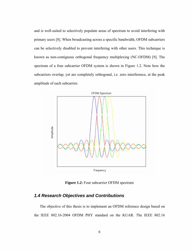


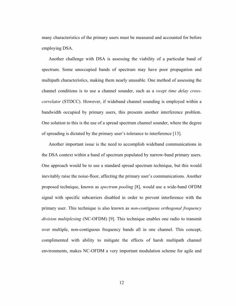


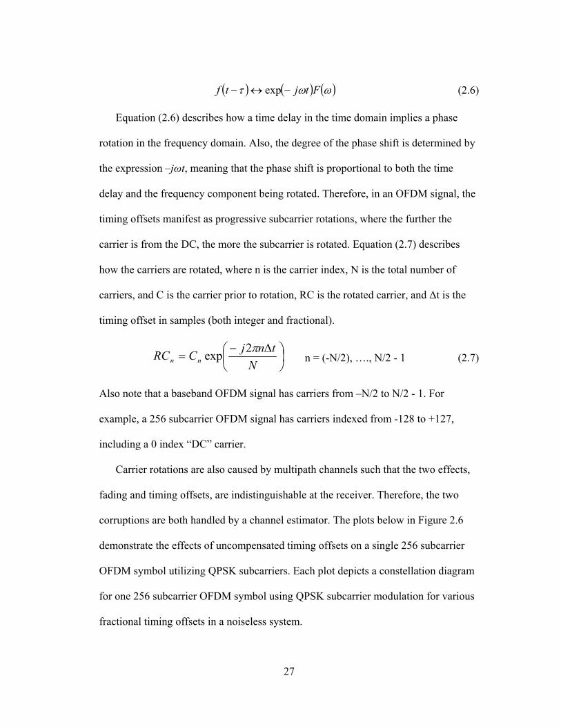

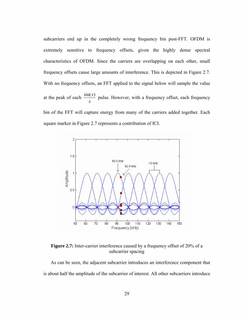


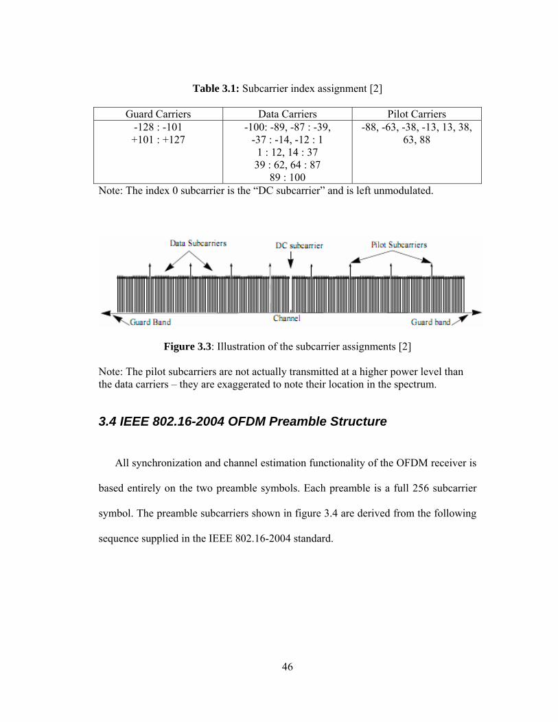
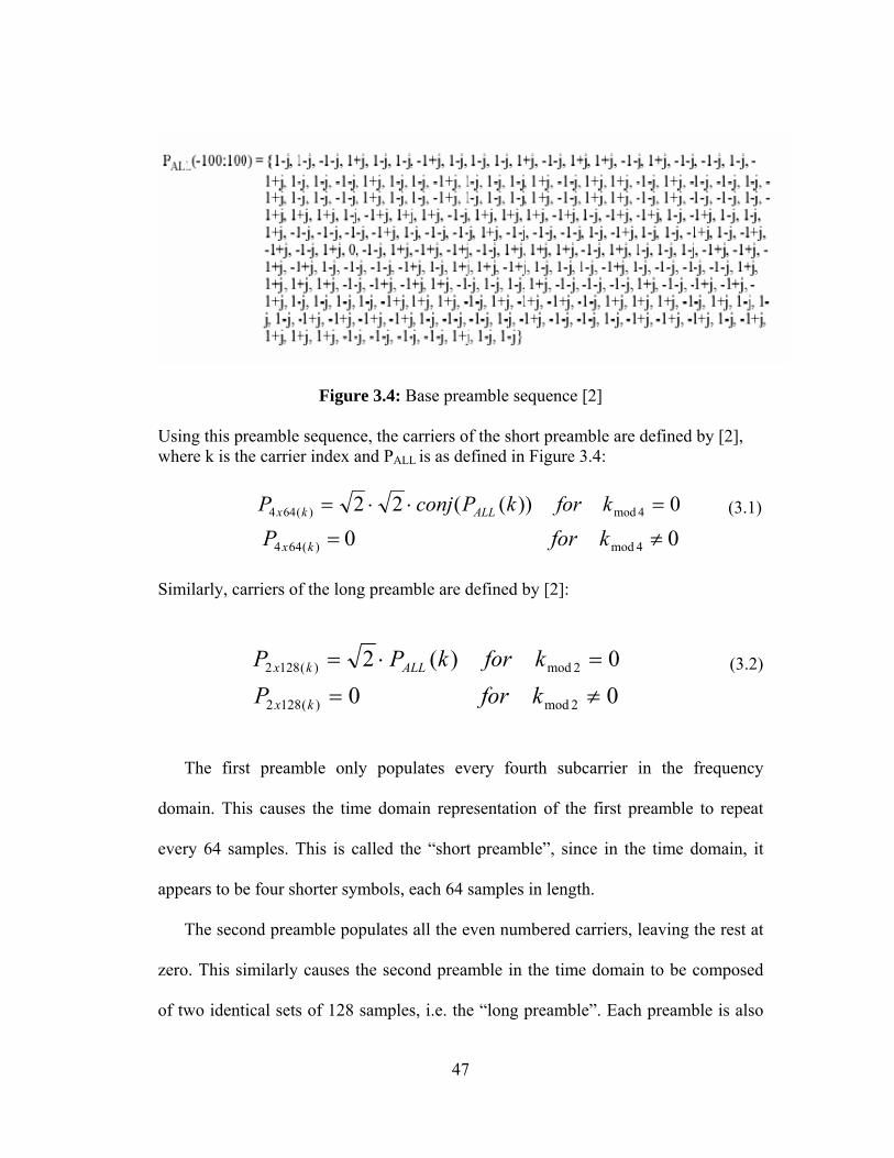


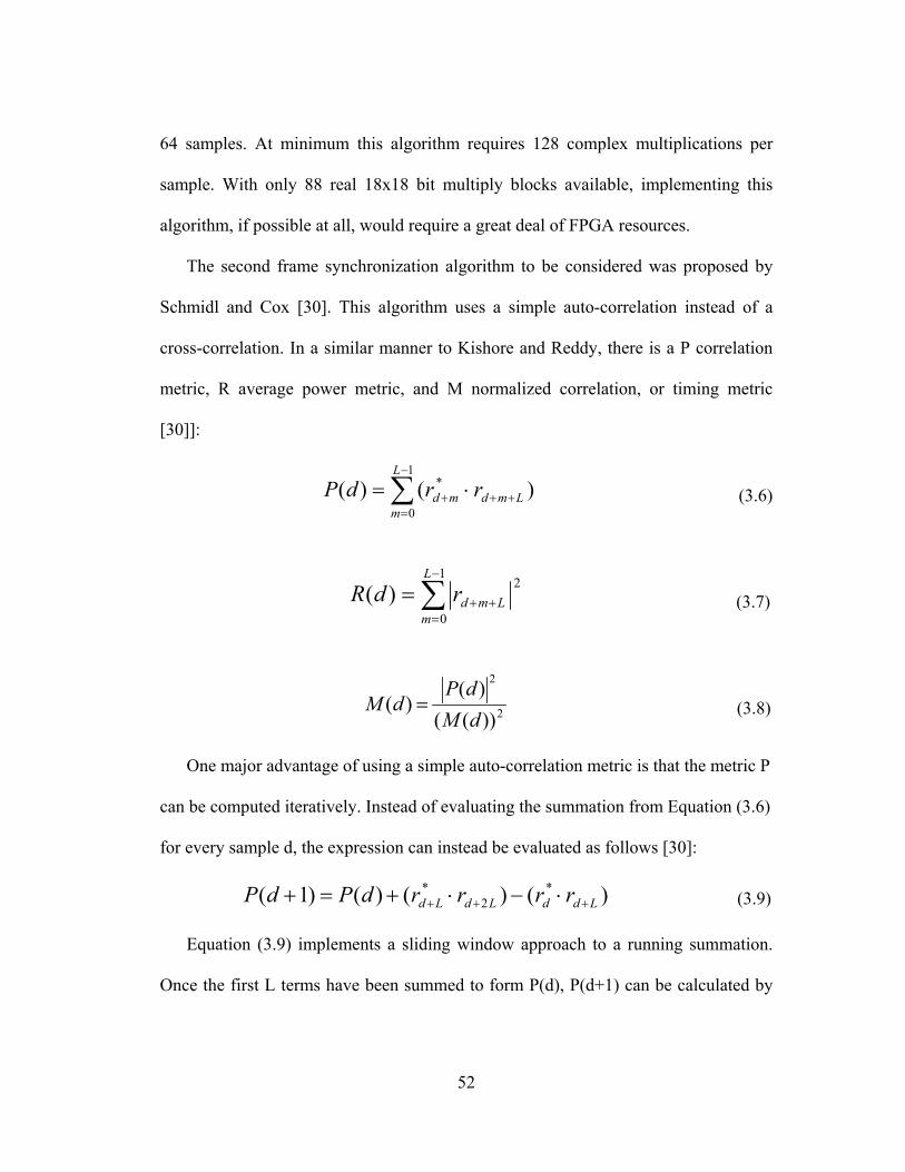


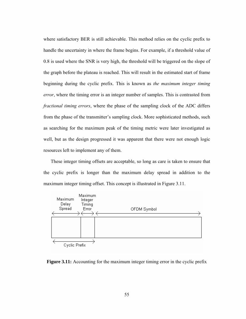


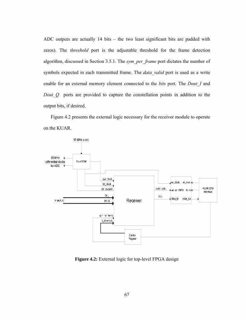
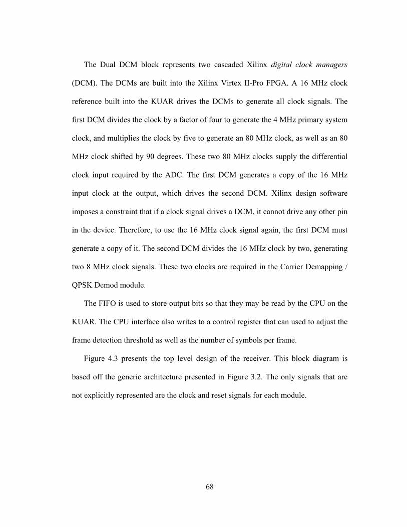
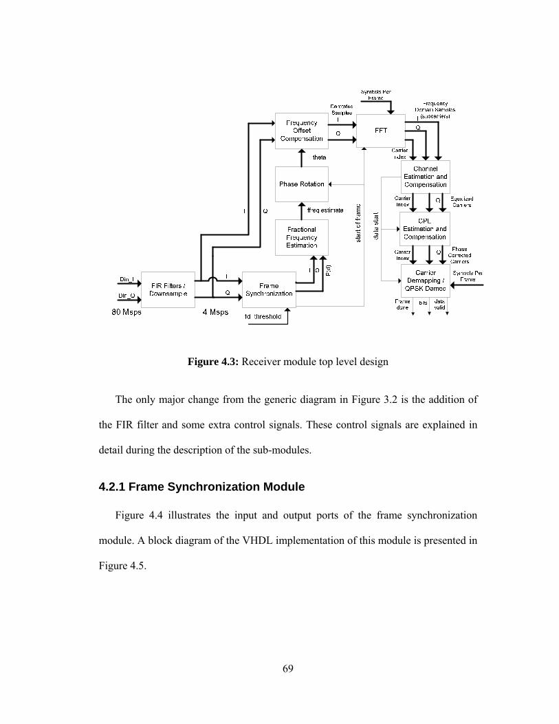


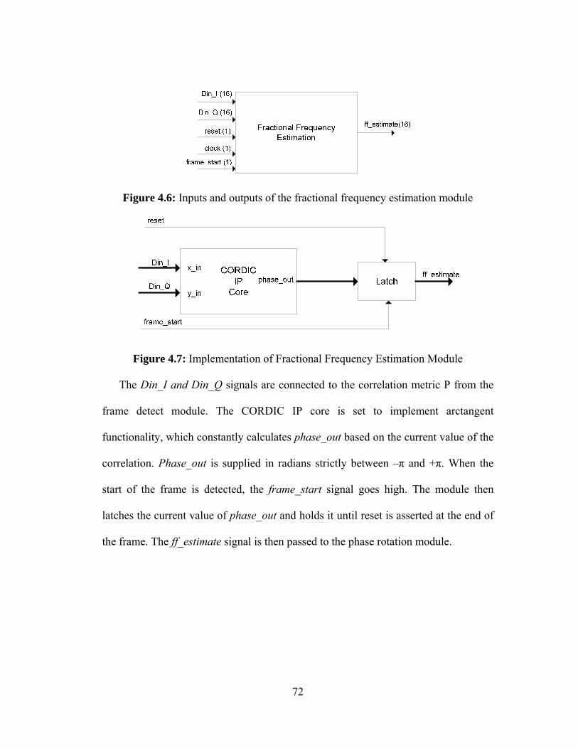


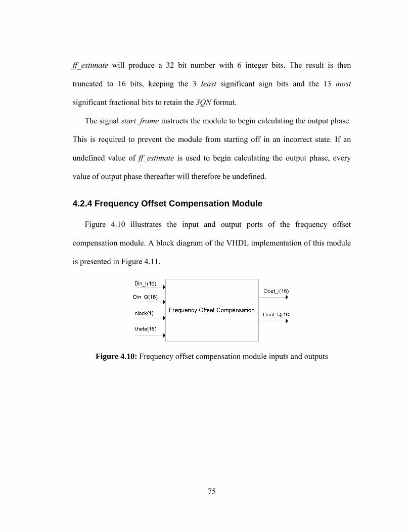
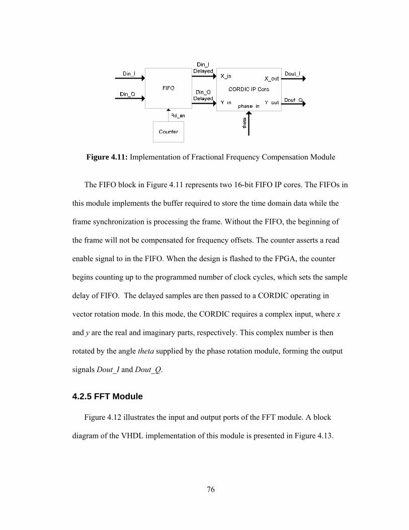


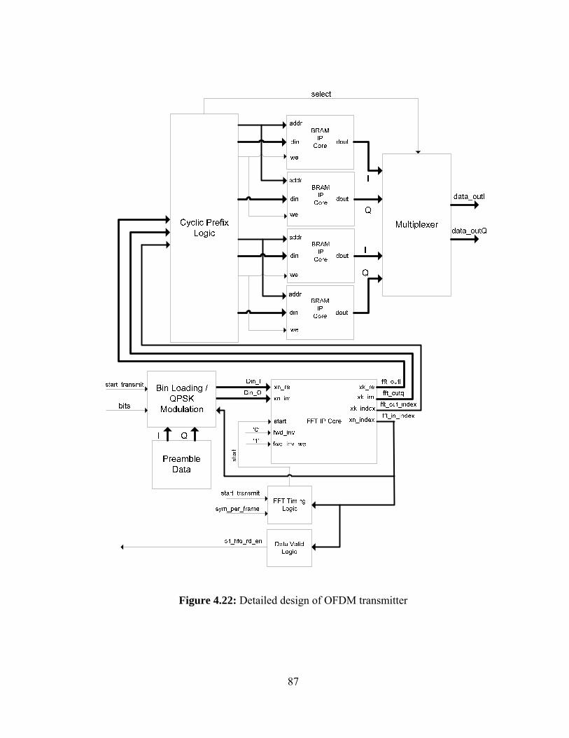


![Research Article TheSS-SCRSchemeforDynamicSpectrumAccess · 2017. 1. 21. · most present day wireless technologies such as IEEE 802.16 [17] and 802.22 [18] are based on OFDM, the](https://static.documents.pub/doc/80x56/5fde35f3a3f51d515e21d8c0/research-article-thess-scrschemefordynamicspectrumaccess-2017-1-21-most-present.jpg)


