PowerSOC Workshop 1 On-Chip Bondwire Magnetics with Ferrite-Epoxy Glob Coating for Power Systems on Chip (SOC) Jian Lu, Hongwei Jia, Andres Arias, Xun Gong and Z. John Shen Florida Power Electronics Center School of Electrical Engineering and Computer Science University of Central Florida Orlando, Florida, USA Contact Email: [email protected]
Transcript
PowerSOC Workshop 1
On-Chip Bondwire Magnetics with
Ferrite-Epoxy Glob Coating for
Power Systems on Chip (SOC)
Jian Lu, Hongwei Jia, Andres Arias, Xun Gong and Z. John Shen
Florida Power Electronics CenterSchool of Electrical Engineering and Computer Science
University of Central FloridaOrlando, Florida, USA
• Cost effective technology of integrating inductors and transformers onto the silicon chip, while achieving adequate performance in terms of inductance, dc series resistance, maximum saturation current, coupling coefficient, and Q factor.
PowerSOC Workshop 3
State of Art: MEMS Magnetics• Sophisticated MEMS technology as a post-processing step after the
completion of the CMOS chip containing all power switching devices and control circuitry.
• MEMS technology allows sequential deposition and patterning of numerous layers of conductor, insulator, permalloy or ferrite thin films to form desirable inductor and transformer structures.
• However, high dc resistance and poor Q factor (typically 3 to 8) of MEMS inductors/transformers severely limit the current handling capability and efficiency of the power SOC.
• More critically, the large increase of fabrication complexity and cost associated with the MEMS post-processing approach raises questions on its feasibility to facilitate large scale commercialization of the power SOC concept into the extremely cost-sensitive power supply market.
PowerSOC Workshop 4
Bondwire Magnetics Concept
Concept of on-chip bondwire magnetic component with ferrite epoxy glob core.
Ferrite epoxy glob core
Power SOC chip
Bondwire windings
PowerSOC Workshop 5
Advantages
• The on-chip bondwire inductors and transformers can be integrated into the power SOC packaging process with minimal changes.
• Aluminum or gold bondwires, due to their relatively large diameters, are much more conductive than the thin metal films in MEMS inductors. Therefore, a much lower dc resistance and higher Q factor can be expected for the bondwire inductors.
• The electromagnetic field of a bondwire inductor or transformer is mainly distributed outside the silicon substrate. The Eddy current loss in the silicon substrate at high frequency, a major concern in MEMS magnetics, can therefore be minimized.
PowerSOC Workshop 6
Prototype on PCB
Fabricated bondwire transformer (Np:Ns=9:1)
With ferrite epoxy
Without ferrite epoxy
PowerSOC Workshop 7
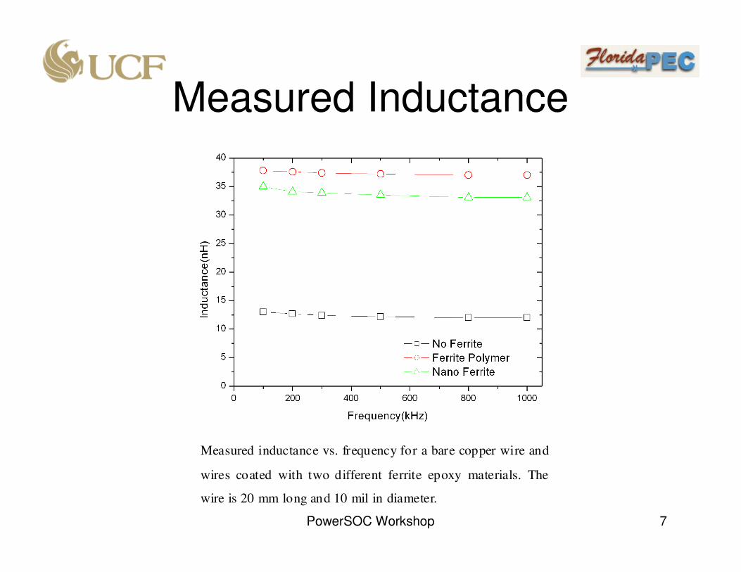
Measured Inductance
Measured inductance vs. frequency for a bare copper wire and
wires coated with two different ferrite epoxy materials. The
wire is 20 mm long and 10 mil in diameter.
PowerSOC Workshop 8
Comparison of the state-of-the-art MEMS micro-inductors, commercial wire wound inductors, and the bondwire inductors in terms of
inductance and dc resistance
PowerSOC Workshop 9
Comparison of Q factors between the state-of-the-art MEMS micro-inductors, commercial wire wound inductors, and the bondwire
inductors.
PowerSOC Workshop 10
Measured switching waveform of the 10 mil bondwire inductors for core saturation characterization
PowerSOC Workshop 11
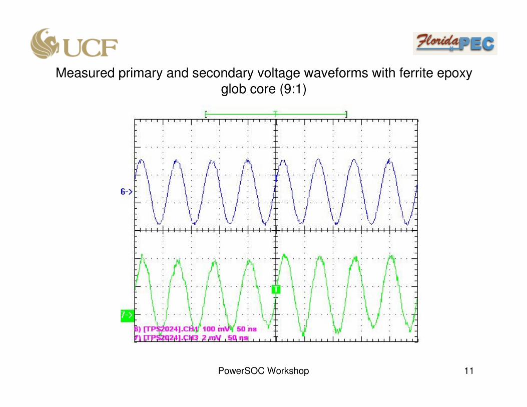
Measured primary and secondary voltage waveforms with ferrite epoxy glob core (9:1)
PowerSOC Workshop 12
A Prototype Single-Chip DC/DC
Converter using Bondwire Inductors
PowerSOC Workshop 13
Conclusion
• We have proposed and investigated the feasibility of a new concept of realizing on-chip inductors and transformers in power SOC’susing existing bondwires with additional ferrite epoxy glob coating both experimentally and with finite element modeling.
• A Q factor of 30-40 is experimentally demonstrated for the bondwireinductors
• Bondwire magnetic components can be easily integrated into IC manufacturing processes with minimal changes, and open possibilities for realizing cost-effective, high current, high efficiency power SOC’s.
• Future work includes studies on the selection of ferrite materials, the influence of the shape and volume of the ferrite beads, the effect of the height and length of the bondwire loop, and possible implementation methods in mass production.