12th International Conference on Field Programmable Logic and Applications On Optimum Designs of Universal Switch Blocks On Optimum Designs of Universal Switch Blocks Hongbing Fan, University of Victoria, Canada Jiping Liu, University of Lethbridge, Canada Yu-Liang Wu and Chak-Chung Cheung The Chinese University of Hong Kong, Hong Kong
Transcript
12th International Conference on Field Programmable Logic and Applications
On Optimum Designs of Universal Switch BlocksOn Optimum Designs of Universal Switch Blocks
Hongbing Fan, University of Victoria, Canada
Jiping Liu, University of Lethbridge, Canada
Yu-Liang Wu and Chak-Chung Cheung
The Chinese University of Hong Kong, Hong Kong
On Optimum Designs of Universal Switch Blocks 2Session 3C - Paper 3
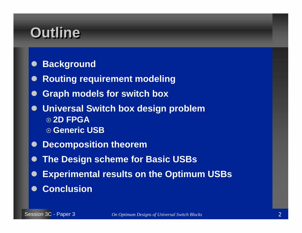
OutlineOutline
� Background
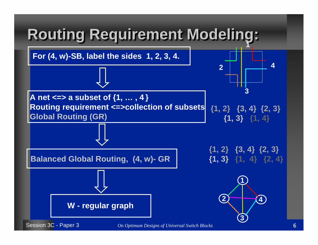
� Routing requirement modeling
� Graph models for switch box
� Universal Switch box design problem� 2D FPGA�Generic USB
� Decomposition theorem
� The Design scheme for Basic USBs
� Experimental results on the Optimum USBs
� Conclusion
On Optimum Designs of Universal Switch Blocks 3Session 3C - Paper 3
Switch box design problem in 2D-FPGASwitch box design problem in 2D-FPGA
Design Goal: to find Switch Boxes (SB) with higher routability and fewer switches .
On Optimum Designs of Universal Switch Blocks 4Session 3C - Paper 3
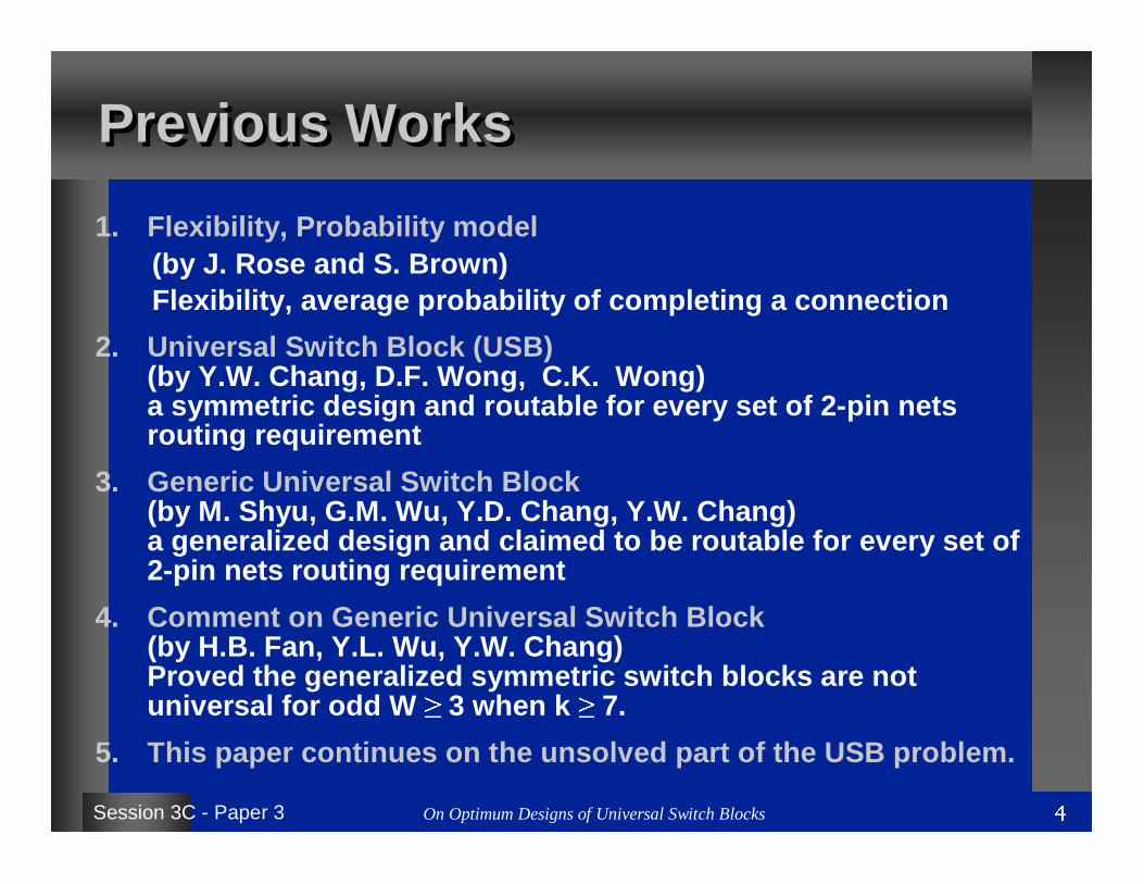
Previous WorksPrevious Works
1. Flexibility, Probability model (by J. Rose and S. Brown)Flexibility, average probability of completing a co nnection
2. Universal Switch Block (USB)(by Y.W. Chang, D.F. Wong, C.K. Wong)a symmetric design and routable for every set of 2- pin nets routing requirement
3. Generic Universal Switch Block(by M. Shyu, G.M. Wu, Y.D. Chang, Y.W. Chang)a generalized design and claimed to be routable for every set of 2-pin nets routing requirement
4. Comment on Generic Universal Switch Block(by H.B. Fan, Y.L. Wu, Y.W. Chang)Proved the generalized symmetric switch blocks are not universal for odd W ≥ 3 when k ≥ 7.
5. This paper continues on the unsolved part of the USB problem.
On Optimum Designs of Universal Switch Blocks 5Session 3C - Paper 3
Generic (k, w)-USB :Generic (k, w)-USB :
Insideswitches
(6,3)-USB
Insideswitches
(4,4)-USB
the USB of k-way and W terminals on each way
routable for every (4,4)-routing requirement
routable for every (6,3)-routing requirement
On Optimum Designs of Universal Switch Blocks 6Session 3C - Paper 3
On Optimum Designs of Universal Switch Blocks 7Session 3C - Paper 3
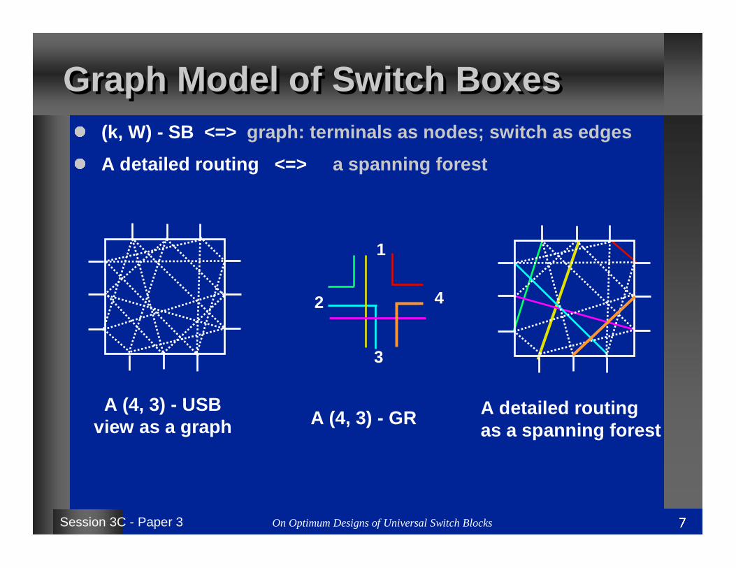
Graph Model of Switch Boxes Graph Model of Switch Boxes � (k, W) - SB <=> graph: terminals as nodes; switch as edges� A detailed routing <=> a spanning forest
2 4
3
1
A (4, 3) - USBview as a graph A (4, 3) - GR A detailed routing
as a spanning forest
On Optimum Designs of Universal Switch Blocks 8Session 3C - Paper 3
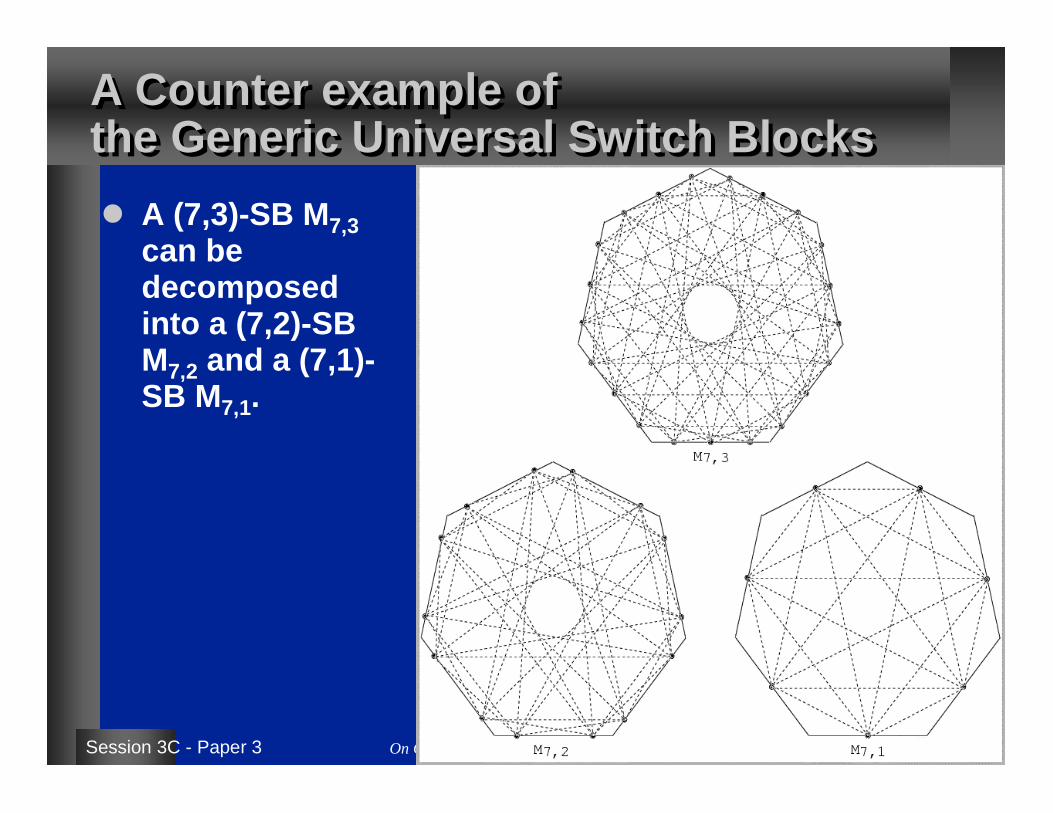
A Counter example of the Generic Universal Switch BlocksA Counter example of the Generic Universal Switch Blocks
� A (7,3)-SB M7,3can be decomposed into a (7,2)-SB M7,2 and a (7,1)-SB M7,1.
On Optimum Designs of Universal Switch Blocks 9Session 3C - Paper 3
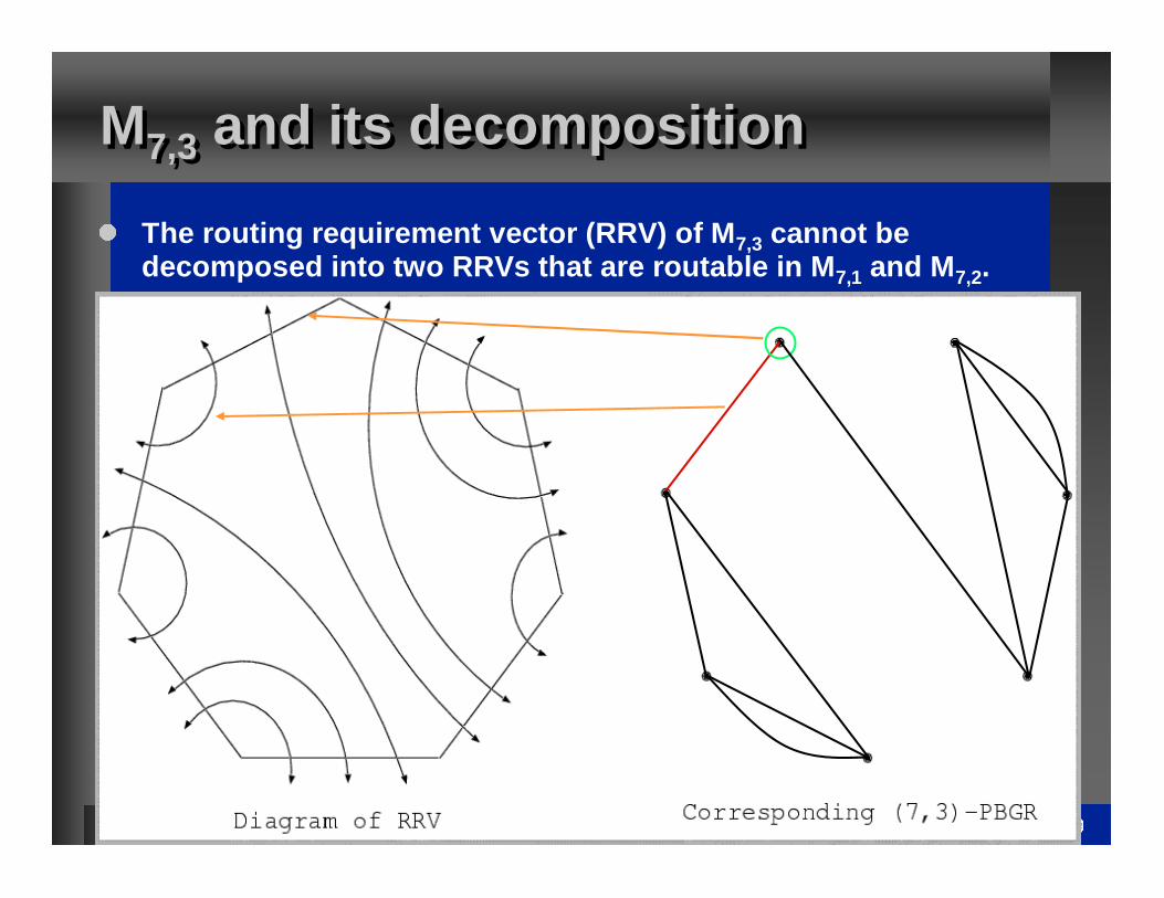
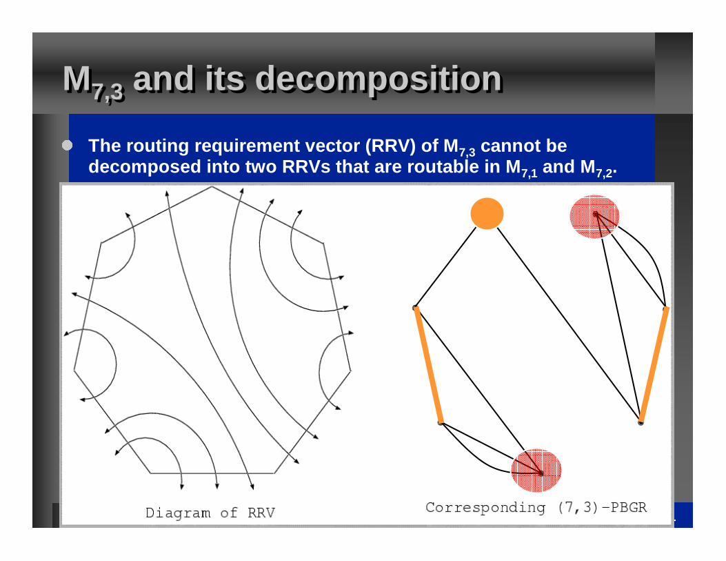
M7,3 and its decompositionM7,3 and its decomposition� The routing requirement vector (RRV) of M 7,3 cannot be decomposed into two RRVs that are routable in M 7,1 and M 7,2.
On Optimum Designs of Universal Switch Blocks 10Session 3C - Paper 3
M7,3 and its decompositionM7,3 and its decomposition� The routing requirement vector (RRV) of M 7,3 cannot be decomposed into two RRVs that are routable in M 7,1 and M 7,2.
On Optimum Designs of Universal Switch Blocks 11Session 3C - Paper 3
M7,3 and its decompositionM7,3 and its decomposition� The routing requirement vector (RRV) of M 7,3 cannot be decomposed into two RRVs that are routable in M 7,1 and M 7,2.
On Optimum Designs of Universal Switch Blocks 12Session 3C - Paper 3
� An k-sided switch block with W terminals on each si de (k,W)-SB is said to be Universal � if every set of (2-pin) nets satisfying the dimensi on
constraint is simultaneously routable on the switc h block.
� For even W,� A (k,2m)-RR can be decomposed into m (k,2)-RRs� A union of m (k,2)-USBs forms a (k,2m)-USB
� For odd W,� There is a minimum integer f2(k) such that a (k,W)-RR can be decomposed into a (k, f2(k))-RR and some (k,2)-RRs.� The problem is: What is the value of f2(k)?
On Optimum Designs of Universal Switch Blocks 13Session 3C - Paper 3
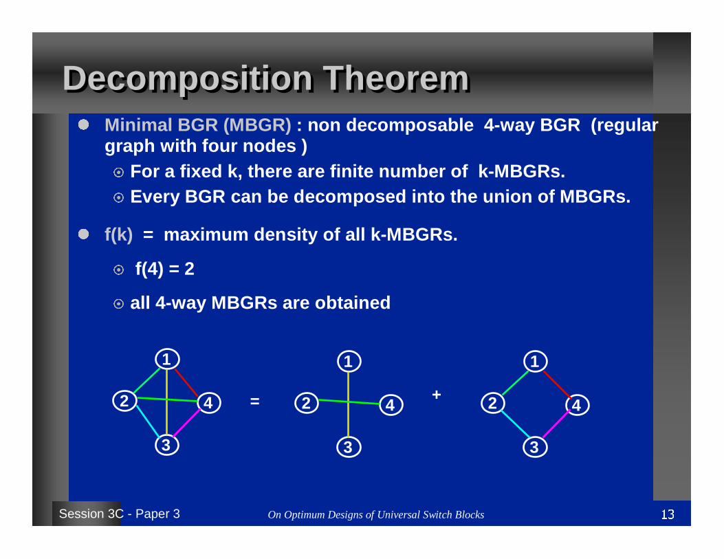
Decomposition TheoremDecomposition Theorem
1
4
3
2
1
4
3
2
1
4
3
2= +
� Minimal BGR (MBGR) : non decomposable 4-way BGR (regular graph with four nodes ) � For a fixed k, there are finite number of k-MBGRs.� Every BGR can be decomposed into the union of MBGRs.� f(k) = maximum density of all k-MBGRs. � f(4) = 2� all 4-way MBGRs are obtained
On Optimum Designs of Universal Switch Blocks 14Session 3C - Paper 3
Decomposition of a (4,4)-USBDecomposition of a (4,4)-USB� From RRV to PMBGRs .
On Optimum Designs of Universal Switch Blocks 15Session 3C - Paper 3
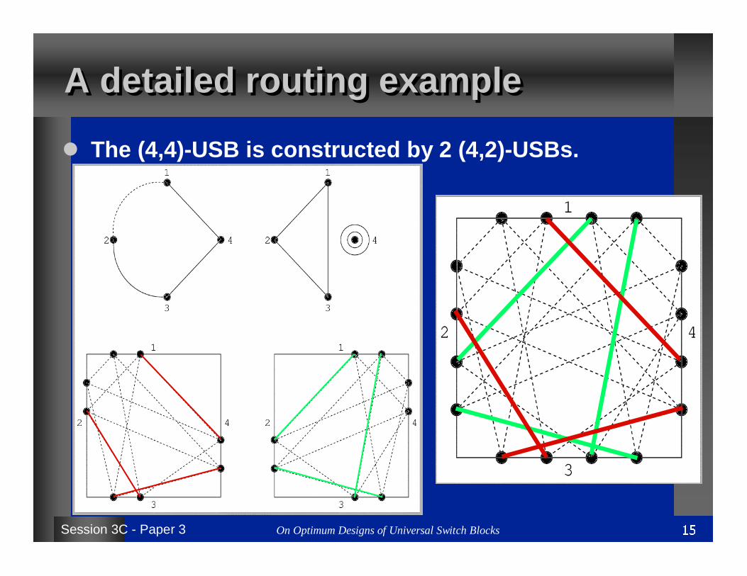
A detailed routing exampleA detailed routing example
� The (4,4)-USB is constructed by 2 (4,2)-USBs.
On Optimum Designs of Universal Switch Blocks 16Session 3C - Paper 3
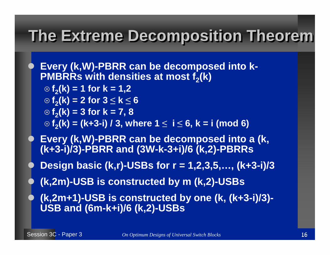
The Extreme Decomposition TheoremThe Extreme Decomposition Theorem
� Every (k,W)-PBRR can be decomposed into k-PMBRRs with densities at most f 2(k)� f2(k) = 1 for k = 1,2� f2(k) = 2 for 3 ≤ k ≤ 6� f2(k) = 3 for k = 7, 8� f2(k) = (k+3-i) / 3, where 1 ≤ i ≤ 6, k = i (mod 6)
� Every (k,W)-PBRR can be decomposed into a (k, (k+3-i)/3)-PBRR and (3W-k-3+i)/6 (k,2)-PBRRs
� Design basic (k,r)-USBs for r = 1,2,3,5,…, (k+3-i)/3
� (k,2m)-USB is constructed by m (k,2)-USBs
� (k,2m+1)-USB is constructed by one (k, (k+3-i)/3)-USB and (6m-k+i)/6 (k,2)-USBs
On Optimum Designs of Universal Switch Blocks 17Session 3C - Paper 3
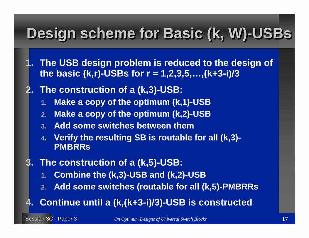
Design scheme for Basic (k, W)-USBsDesign scheme for Basic (k, W)-USBs
1. The USB design problem is reduced to the design of the basic (k,r)-USBs for r = 1,2,3,5,…,(k+3-i)/3
2. The construction of a (k,3)-USB:1. Make a copy of the optimum (k,1)-USB2. Make a copy of the optimum (k,2)-USB3. Add some switches between them4. Verify the resulting SB is routable for all (k,3)-
PMBRRs
3. The construction of a (k,5)-USB:1. Combine the (k,3)-USB and (k,2)-USB2. Add some switches (routable for all (k,5)-PMBRRs
4. Continue until a (k,(k+3-i)/3)-USB is constructed
On Optimum Designs of Universal Switch Blocks 18Session 3C - Paper 3
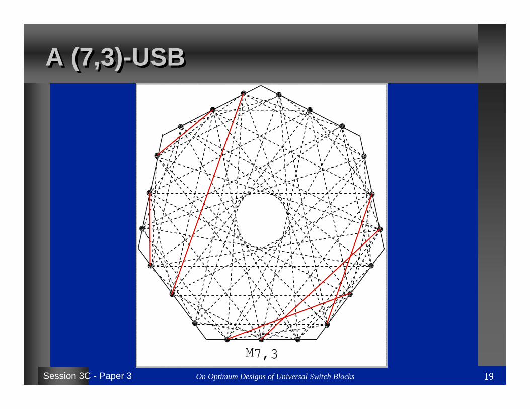
Example: a (7,3)-USBExample: a (7,3)-USB
� (7,3)-USB can be constructed by (7,1)-USB + (7,2)-USB, and add some switches (not unique) to ensure the USB is routable for all (7,3)-PMBRRs.
On Optimum Designs of Universal Switch Blocks 19Session 3C - Paper 3
A (7,3)-USBA (7,3)-USB
On Optimum Designs of Universal Switch Blocks 20Session 3C - Paper 3
The previous unsolved problemThe previous unsolved problem
On Optimum Designs of Universal Switch Blocks 21Session 3C - Paper 3
Experiment with USBsExperiment with USBs� Run “ VPR” on FPGAs with the proposed alternative USBs� use 21 MCNC benchmark circuits� Compare the number of tracks required to route the circuits on FPGAs with disjoint S-Box (XC4000 type) and Symmetr ic USB designs
Disjoint (4, 8)-SB Symmetric (4, 8)-USB Alternative (4, 8)-USB
On Optimum Designs of Universal Switch Blocks 22Session 3C - Paper 3
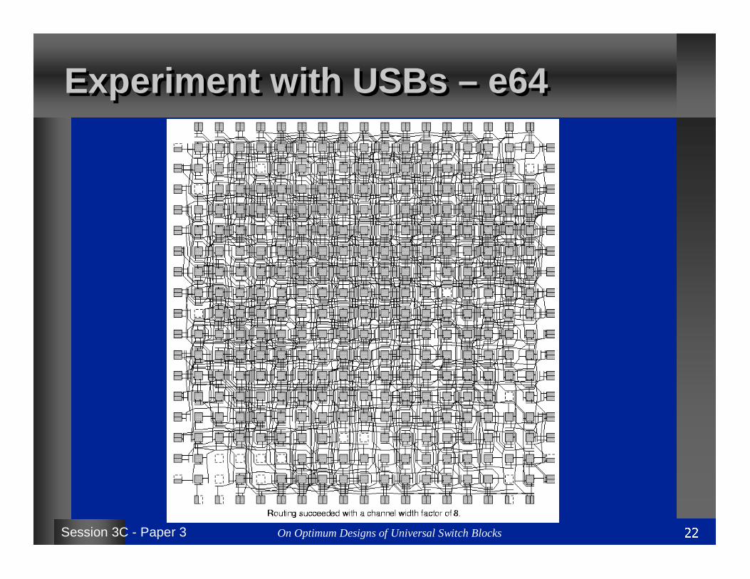
Experiment with USBs – e64Experiment with USBs – e64
On Optimum Designs of Universal Switch Blocks 23Session 3C - Paper 3
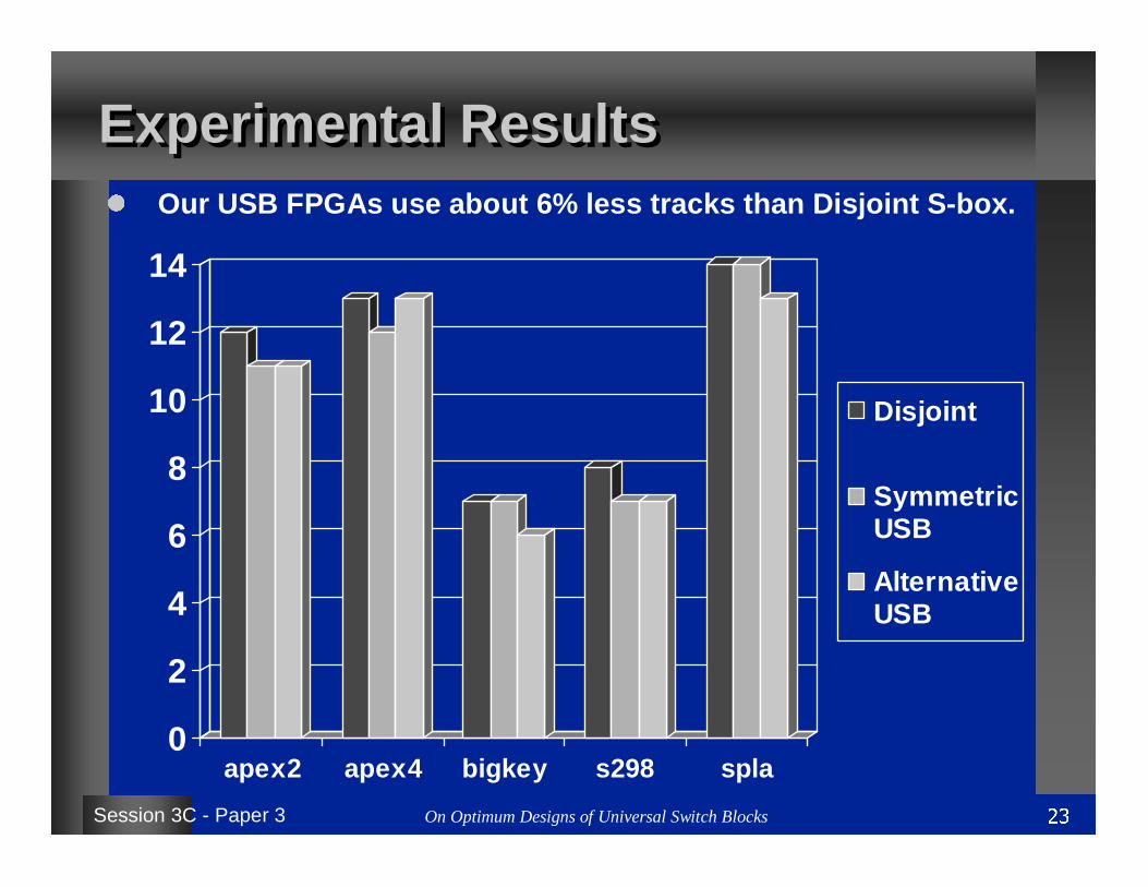
Experimental ResultsExperimental Results
0
2
4
6
8
10
12
14
apex2 apex4 bigkey s298 spla
Disjoint
SymmetricUSB
AlternativeUSB
� Our USB FPGAs use about 6% less tracks than Disjoin t S-box.
On Optimum Designs of Universal Switch Blocks 24Session 3C - Paper 3
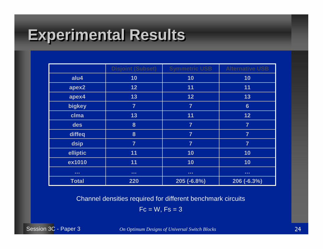
Experimental ResultsExperimental Results
220
…
11
11
7
8
8
13
7
13
12
10
Disjoint (Subset)
206 (-6.3%)205 (-6.8%)Total
………
1010ex1010
1010elliptic
77dsip
77diffeq
77des
1211clma
67bigkey
1312apex4
1111apex2
1010alu4
Alternative USBSymmetric USB
Channel densities required for different benchmark circuits
Fc = W, Fs = 3
On Optimum Designs of Universal Switch Blocks 25Session 3C - Paper 3
Conclusions Conclusions 1. The Optimum USB design problem is solved for odd
and even channel densities.
2. The extreme decomposition theorem has reduced the USB design problem to the basic USB design problem.
3. The inductive design scheme is used for designing basic USBs.
4. Experiments show the local optimized USB can bring the improvement of global routability.
On Optimum Designs of Universal Switch Blocks 26Session 3C - Paper 3