On the Electron-Transfer Mechanism in the Contact-Electrification Effect
Cheng Xu, Yunlong Zi, Aurelia Chi Wang, Haiyang Zou, Yejing Dai, Xu He, Peihong Wang, Yi-Cheng Wang, Peizhong Feng, Dawei Li, and Zhong Lin Wang*
Dr. C. Xu, Dr. Y. Zi, A. C. Wang, H. Zou, Dr. Y. Dai, X. He, Dr. P. Wang, Dr. Y.-C. Wang, Prof. Z. L. WangSchool of Materials Science and EngineeringGeorgia Institute of TechnologyAtlanta, GA 30332-0245, USAE-mail: [email protected]. C. Xu, Prof. P. FengSchool of Materials Science and EngineeringChina University of Mining and TechnologyXuzhou 221116, ChinaDr. Y. ZiDepartment of Mechanical and Automation EngineeringThe Chinese University of Hong KongShatin, N.T., Hong Kong SAR, ChinaProf. D. LiKey Laboratory of Materials for High Power LaserShanghai Institute of Optics and Fine MechanicsChinese Academy of SciencesShanghai 201800, ChinaProf. Z. L. WangBeijing Institute of Nanoenergy and NanosystemsChinese Academy of SciencesBeijing 100083, China
The ORCID identification number(s) for the author(s) of this article can be found under https://doi.org/10.1002/adma.201706790.
DOI: 10.1002/adma.201706790
Although contact-electrification (CE) (or triboelectrification) has been a documented phenomenon since the ancient Greek era of 2600 years ago, there still exist many debates regarding the origins of this effect, the most important issue being whether the charge transfer occurs through electrons or ions and why the charges retain on the sur-face without a quick dissipation. The con-cept of electron transfer was well accepted in explaining metal–metal and metal–semi-conductor electrification, as determined by the work function or contact potential difference,[1,2] which could be extended to explain the metal-insulator electrification to some extent using the existence of surface states.[3–6] Ion transfer was also proposed to explain electrification, particularly which occurred involving polymers.[7,8] Ions con-taining functional groups were believed to contribute to CE.[9–11] These discrepan-cies have continued to raise doubts about whether electron or ion transfer is the dom-inant underlying mechanism in CE.
It is worth noting that nearly all of these studies were based on quantitative analysis of generated charge amount, including the correlation of charge amount with bandgaps, work function, and ion densities[12,13] and electrochemical reactions.[14,15] It is also interesting to note that there are few time-dependent and/or temperature-dependent studies on the variation of surface electrostatic charges.[16] Here, we believe that the key to solving the debate may lie in developing a new method that can quanti-tatively obtain the surface charge density/amount in real time, particularly under different temperatures. Accordingly, time-dependent studies on charge transfer may be accomplished through a newly developed triboelectric nanogenerator (TENG) as an application of Maxwell’s displacement current,[17–23] due to the fact that the TENG’s outputs are dictated by the sur-face charge density.[24] Recently, TENG has been utilized to investigate CE at relatively low temperatures.[25–27] However, an in-depth study on the mechanism of CE is required to be performed at high temperatures, at which electron emission is possible. In such temperature range, the discharge of electrons or ions may follow distinct laws and they can be easily modeled and separated.
In this study, by designing a TENG that worked under high temperatures, real-time quantitative measurements of the sur-face charge density/amount were realized, facilitating a possible
A long debate on the charge identity and the associated mechanisms occurring in contact-electrification (CE) (or triboelectrification) has persisted for many decades, while a conclusive model has not yet been reached for explaining this phenomenon known for more than 2600 years! Here, a new method is reported to quantitatively investigate real-time charge transfer in CE via triboelectric nanogenerator as a function of temperature, which reveals that electron transfer is the dominant process for CE between two inorganic solids. A study on the surface charge density evolution with time at various high temperatures is consistent with the electron thermionic emission theory for triboelectric pairs composed of Ti–SiO2 and Ti–Al2O3. Moreover, it is found that a potential barrier exists at the surface that prevents the charges generated by CE from flowing back to the solid where they are escaping from the surface after the contacting. This pinpoints the main reason why the charges generated in CE are readily retained by the material as electrostatic charges for hours at room temperature. Furthermore, an electron-cloud–potential-well model is proposed based on the electron-emission-dominatedcharge-transfer mechanism, which can be generally applied to explain all types of CE in conventional materials.
discovery of the charge identity and mechanism in CE. The TENG was designed to reflect the discharge performance of the surface electrostatic charges at high temperature; and the results were found to be consistent with the thermionic emis-sion equation of electrons for the TENGs designed in the study. Moreover, it was found that different materials had different potential barrier heights at the surfaces, which would prevent the charges generated by CE from flowing back or dissipating. Furthermore, an electron-cloud–potential-well model was proposed based on the electron emission dominated charge transfer mechanism, which could be applied to understand all types of CE in general materials.
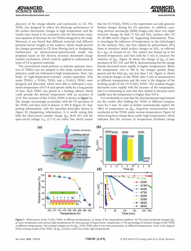
The conventional metal–polymer or polymer–polymer struc-ture of TENGs was not adopted in this study, mainly because polymers could not withstand at high temperatures. Here, two kinds of high-temperature-resistant contact–separation (CS) mode TENGs, a Ti-SiO2 TENG, and a Ti-Al2O3 TENG, were designed and fabricated, which were able to withstand a max-imum temperature of 673 K and operate stably for a long period of time. Each TENG was placed in a heating cabinet, which could provide the desired temperature with an accuracy of ±5 K. The structure of the Ti-SiO2 TENG is shown in Figure 1a. The charges increasingly accumulate with the CS operation of the TENG and then tend to balance at 293 K (Figure S1, Sup-porting Information), with the operation principles shown in Figure S2 (Supporting Information). It is worth noting that both the short-circuit transfer charge QSC (0.45 nC) and the open-circuit voltage VOC (1.3 V) are rather low, which means
that the CS Ti-SiO2 TENG in the experiment can only generate limited charges during the CS operation. In addition, scan-ning electron microscopy (SEM) images only show very slight structure change for both Ti foil and SiO2 surfaces after CE for 20 000 circles (Figure S3, Supporting Information). Thus, to investigate the influence of temperature on the tribocharges on the surfaces, SiO2 was first rubbed by polyurethane (PU) foam to introduce initial surface charges on SiO2, as reflected by a QSC of around 45 nC. The cabinet was heated up to the desired temperature, and then held for 5 min to measure the variation of QSC. Figure 1b shows the change of QSC at tem-peratures of 353, 533, and 583 K, demonstrating that the charge density decreased more rapidly at higher temperatures. When the temperature rose to 583 K, the charges quickly disap-peared and the total QSC was less than 1 nC. Figure 1c shows the residual charges on the TENG after 5 min of measurement at different temperatures and the inset is the diagram of the working model of the CS Ti-SiO2 TENG. The residual charges decreased more rapidly with the increase of the temperature, and it is interesting to note that they started to decrease more rapidly once the temperature is higher than 533 K.
It is worthwhile to note that the aforementioned experiments are the results after holding the TENG at different tempera-tures for 5 min. In order to further systematically explore the effect of temperature on QSC, long-term measurements were conducted on the TENG under various temperatures. Figure 1d shows long-term charge decay under high temperatures, which indicates that the increase of temperature facilitates charge
Adv. Mater. 2018, 1706790
Figure 1. Performance of the Ti-SiO2 TENG at different temperatures. a) Setup of the measurement platform. b) The total transferred changes QSC at room temperature and various high temperatures for three groups of experiments, respectively. c) The percentage of residual charges of the TENG at different temperatures. The residual charges are the QSC of the TENG after 5 min heat preservation at different temperatures. Inset is the diagram of the working model of the TENG. d) QSC evolution with time under high temperatures.
decay. It also reveals that the QSC response is analogous to exponential decay under high temperatures. In addition, taking the temperature of 503 K as an example, all of QSC, VOC, and short-circuit current ISC share the same decay characteristics, which features a slow-fast-slow trend in decay speed (Figure S4, Supporting Information).
To estimate whether charge decays are consistent with the electron thermionic emission model, the measured QSC values are fitted according to the thermionic emission equation[28,29]
e e 102J A T
W
kT
W
kTλ= −
∆
(1)
where J is the current density, λ is the material-specific correc-tion factor, A0 is Richardson constant of a free electron, T is the temperature, W is the height of the potential barrier, k is Boltz-mann constant, and ΔW is the potential barrier height variation
due to the surface electric field E. Since 0
SCE Qσε
∝ ∝ (Note S1,
Supporting Information), we may assume that ΔW = λ1QSC/λ
(λ1 is a constant). When ΔW ≪ kT, e 1W
kT −∆
≈ W
kT
∆, then
e1 0SCJ
A
kT Q
qV
kTλ= (2)
or equivalently
ln ln0
1SC
J
A T
qV
kT kQ
λ
= − +
(3)
where q is the electronic charge. By assuming 1 d
dSC
SCJA
Q
tSQ= = ,
where A is the surface area and S is used to replace e1 0A
kT
qV
kTλ
,
then
eSC SC0Q QSAt= − (4)
where QSC0 is the initial value of QSC. According to Equation (4), QSC follows an exponential decay during thermionic emission. Simulated charge decay curves at the temperatures of 413, 473, 533, and 563 K are shown in Figure 2a–c and Figure S5 (Sup-porting Information), respectively. It is found that the simu-lated data are consistent with the measured data, except for the QSC values during the initial few minutes. This inconsistency may be due to the temperature destabilization during the short-period heat preservation, which may result in a lower average temperature compared to the measured value. With the con-trol experiments extending heat preservation from 5 to 25 min under temperatures of 443 and 473 K, both time-changing curves of QSC are much more consistent with exponential decay (Figure S6, Supporting Information). In addition, according to Equation (3), the plots of ln (J/A0/T) against 1/T are shown in Figure 2d. These plots illustrate that the measured data fit the
Adv. Mater. 2018, 1706790
Figure 2. The measured (dots) and simulated (line) data of the Ti-SiO2 TENG. QSC as a function of the time at various temperatures: a) 413 K, b) 473 K, and c) 533 K. d) Plots of ln (J/A0/T) against 1/T.
thermionic emission equation very well. The height of the bar-rier W is calculated to be 0.81 ± 0.06 eV.
Moreover, if the thermionic emission mechanism is appli-cable here, the surface charge density/amount decay should be affected by the contact/separation status of the two surfaces, since CE may generate additional surface charges during the contact of the surfaces. Therefore, further experimentation was conducted to investigate how the status of the TENG affected the surface charge decay, as reflected by QSC. The effect of the contact/separation status of the two surfaces in four dif-ferent cases before measuring QSC was studied (Figure 3a). Case A started with the two surfaces being separated at 293 K; and raised the temperature until 473 K, the temperature was maintained at 473 K for 5 min before testing. Case B started with the surfaces contacted at 293 K; and raised the tempera-ture until 473 K, the temperature was maintained at 473 K for 5 min before testing. Case C and Case D were similar to Case A and Case B, respectively, but the maintenance time at 473 K increased to 35 min. These four cases are also described in Table 1. The measured QSC values in Case D are the largest for all of the cases; in other words, the contact status of the two surfaces slows down the discharge from SiO2 surface. Conversely, the QSC values in Case C are the smallest, that is, the separation status of the two surfaces facilitates the dis-charge from SiO2 surface. To further investigate this effect, we explored the decay of QSC at 473 K when the surfaces were kept either contacted or separated during the time periods for QSC measurements (Figure 3b). It is demonstrated directly that the QSC decay slowed down during contact, while the decay notice-ably speeded up during separation. Based on these results, we believe that the negative charges on SiO2 surface are electrons rather than ions as follows: (i) In this study, the charges on SiO2
surface were generated by PU-SiO2 triboelectrification. It con-tradicts to the conventional ion transfer model that should con-tain at least mobile ions,[30,31] since PU is a nonionic polymer. McCarty and Whitesides developed the ion transfer model for even nonionic polymer, in which the hydronium and hydroxide ions were attributed to the water from the humid atmosphere: 2H2O ⇌ H3O+ + OH−.[32] However, since the temperature in the experiment is always higher than 373 K (the boiling point of water) and the local relative humidity is less than 1.5% in the furnace, such ion transfer model seems impossible; (ii) assuming an unlikely situation that there are indeed some ions originated from PU itself during the CE, according to the ion transfer model demonstrated by Harper (Figure S7, Sup-porting Information), these ions can transfer to the opposite Ti surface when the distance is less than 10 nm under contact status.[33,34] Once the two surfaces are separated more, the ion emission becomes less possible due to the greatly increased barrier height, which will result in slower QSC decrease under separation status than that in contact status. Apparently, the above discussions contrast with our experimental results, so the ion transfer model cannot explain the phenomena we observed for inorganic solid–solid cases.
Another experiment was conducted to further verify the ther-mionic emission mechanism by replacing SiO2 with Al2O3 to fabricate a Ti-Al2O3 TENG. It is noteworthy that with a better thermal conductivity and thinner thickness, a faster thermal equilibrium will be reached for Al2O3. The QSC (0.16 nC) and the VOC (3.3 V) generated by the Ti-Al2O3 TENG at 293 K are also very low (Figure S8, Supporting Information), which can be ignored during testing. Similar to that of the Ti-SiO2 TENG, an initial charge amount of around 12 nC was introduced by PU-Al2O3 triboelectrification before the TENG operation. Fol-lowing this, the temperature was increased and held for 5 min to measure the QSC variation. Figure 4a demonstrates that the residual charges decrease more rapidly at higher temperatures. The inset in Figure 4a shows the variations of QSC at 353, 443, and 533 K, indicating that at 533 K, the charges decay rapidly to around 1 nC. Figure 4b shows the long-term charge decay of the Ti-Al2O3 TENG at different temperatures. The experimental results are fitted to an exponential decay, which is similar to the data of the Ti-SiO2 TENG, and the QSC decays faster at higher temperatures. A little difference is that, taking the temperature
Adv. Mater. 2018, 1706790
Figure 3. Contacting processes between Ti foil and SiO2 on QSC. a) The change of QSC with time in the four different cases outlined in Table 1. b) QSC evolving with time at 473 K when Ti foil either contacts or separates with SiO2 during the interval of measurements.
Table 1. Status of Ti foil and SiO2 in the four cases.
Cases Step 1: 293–473 K Step 2: 473 K Step 3: 473 K
A Separated for 25 min Separated for 5 min Did measurement
B Contacted for 25 min Contacted for 5 min Did measurement
C Separated for 25 min Separated for 35 min Did measurement
D Contacted for 25 min Contacted for 35 min Did measurement
of 503 K as an example, all of QSC, VOC, and ISC share the same fast-slow trend in decay speed (Figure S9, Supporting Informa-tion). It further confirms that the slow-fast-slow trend in decay speed of the Ti-SiO2 TENG performances is due to the tem-perature destabilization. Figure 4c–e shows the measured and simulated QSC decays at temperatures of 413, 473, and 533 K. The data from the Ti-Al2O3 TENG evidently fit to the theory even better than that of the Ti-SiO2 TENG. Figure 4f shows the plots of ln (J/A0/T) against 1/T, which demonstrates that the charges on Al2O3 are also consistent with the thermionic emis-sion equation, with a lower potential barrier of 0.42 ± 0.02 eV.
Here, we further discuss why the ion transfer mechanism fails to explain the CE data presented above for inorganic solid–solid cases. As shown in Figure 3, it verifies that the mecha-nism of the surface discharging follows the electron thermionic emission model, which rules out the possibility of ions as the charge carriers in CE. In addition, ion transfer satisfies the Boltzmann distribution,[32] which indicates that more tribo-electric charges would be transferred at higher temperature. However, experimental results demonstrated that there were only less charges being transferred during triboelectrification at higher temperature.[27] Furthermore, since the water plays a very important role in the ion transfer model,[35,36] here we make more discussions. Nguyen and Yang demonstrated that there were less charges being transferred at higher moisture level and the maximum charge transfer occurred at ≈0% rela-tive humidity.[37] Baytekin et al. further verified CE did not need the presence of water to occur by providing a water-free envi-ronment using paraffin oil.[38] Moreover, Wen et al. found that the CE of Al-poly(tetrafluoroethylene) (PTFE) could generate
electricity at 500 K[39] and by using our high-temperature-resistant sliding mode TENG, the CE of Ti-SiO2 could happen even at 623 K (Figure S10, Supporting Information). Recent studies by Wang et al. indicated CE at a vacuum of 10−6 Torr was five times higher than that at one atmosphere pressure.[40] All of these phenomena indicate that water is not necessary for CE and the ion transfer mechanism fails to explain the CE observed on larger surfaces.
On the other hand, more recent studies support the elec-tron transfer mechanism. As demonstrated by scanning Kelvin probe microscopy, the sign of the transferred charges in CE could be reversed by applying an electric field.[41] Further studies found that the work required to separate the charged surfaces was comparable to the fracture energies of materials, which revealed that the electrification was associated to the interactions in electron clouds.[42] These studies indicate that the electrification is strongly related to the electron transfer during the overlap of the electron cloud and the formation or fracture of the bonds, which further rule out the ion transfer mechanism. Therefore, we believe that the CE is dominated by electron transfer for the case of solid–solid. But situation could be different in the CE between liquid and solid.
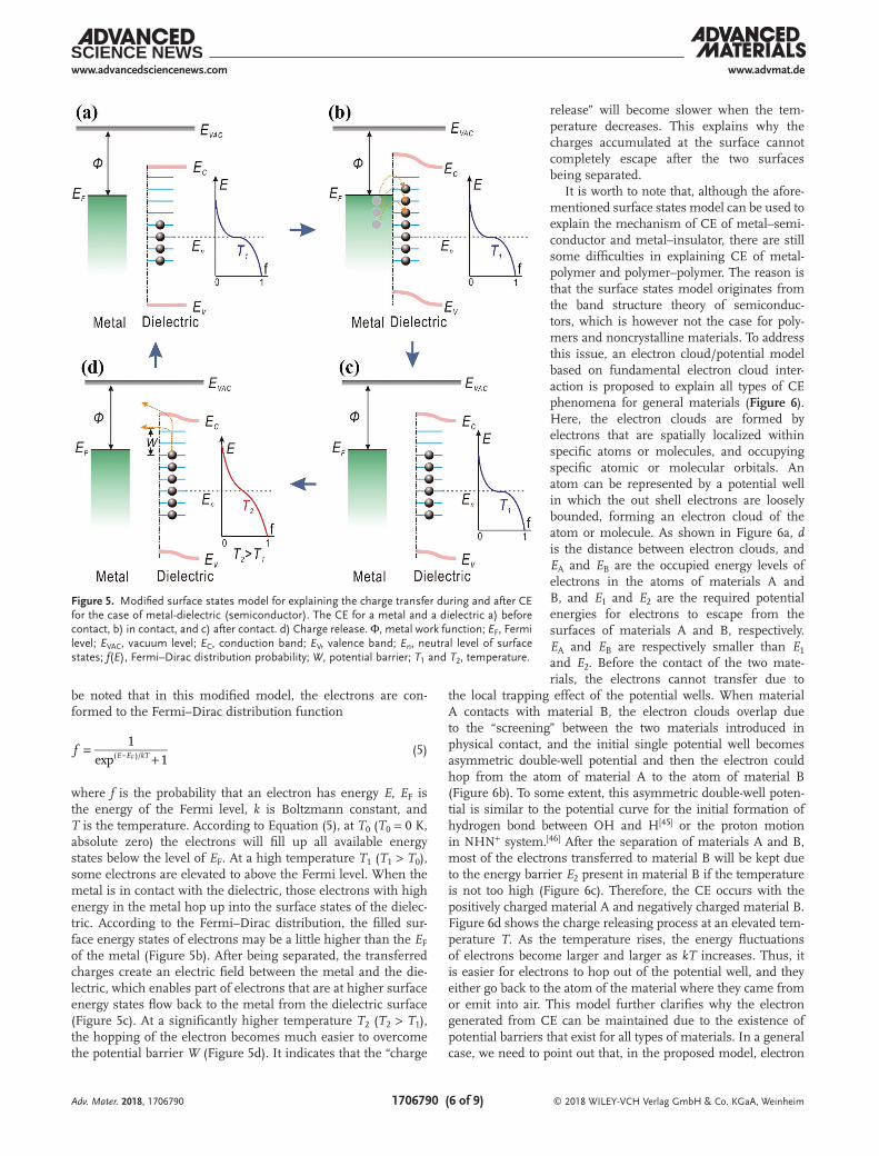
Surface states model[43,44] has been proposed to illustrate the fundamental charge transfer process in CE between a metal and a dielectric (semiconductor). Figure 5a is a diagram showing the energy band before the mutual contact between a metal and a dielectric. Despite the comparatively large equiva-lent bandgap of the dielectric, its highest filled surface energy states are usually lower than the Fermi levels EF of metals, con-sidering fewer electrons remain in the surface states. It should
Adv. Mater. 2018, 1706790
Figure 4. Experimental and simulated data of the Ti-Al2O3 TENG. a) The percentage of residual charges of the TENG at different temperatures. The residual charges are the QSC of the TENG after 5 min heat preservation at different temperatures. Inset is the change of QSC at various temperatures. b) QSC evolution with time at different temperatures. c–e) The measured (dots) and simulated (line) QSC as a function of the time at various tempera-tures of 413, 473, and 533 K. f) Plots of ln (J/A0/T) against 1/T.
be noted that in this modified model, the electrons are con-formed to the Fermi–Dirac distribution function
1exp 1( )/F
f E E kT=+− (5)
where f is the probability that an electron has energy E, EF is the energy of the Fermi level, k is Boltzmann constant, and T is the temperature. According to Equation (5), at T0 (T0 = 0 K, absolute zero) the electrons will fill up all available energy states below the level of EF. At a high temperature T1 (T1 > T0), some electrons are elevated to above the Fermi level. When the metal is in contact with the dielectric, those electrons with high energy in the metal hop up into the surface states of the dielec-tric. According to the Fermi–Dirac distribution, the filled sur-face energy states of electrons may be a little higher than the EF of the metal (Figure 5b). After being separated, the transferred charges create an electric field between the metal and the die-lectric, which enables part of electrons that are at higher surface energy states flow back to the metal from the dielectric surface (Figure 5c). At a significantly higher temperature T2 (T2 > T1), the hopping of the electron becomes much easier to overcome the potential barrier W (Figure 5d). It indicates that the “charge
release” will become slower when the tem-perature decreases. This explains why the charges accumulated at the surface cannot completely escape after the two surfaces being separated.
It is worth to note that, although the afore-mentioned surface states model can be used to explain the mechanism of CE of metal–semi-conductor and metal–insulator, there are still some difficulties in explaining CE of metal-polymer and polymer–polymer. The reason is that the surface states model originates from the band structure theory of semiconduc-tors, which is however not the case for poly-mers and noncrystalline materials. To address this issue, an electron cloud/potential model based on fundamental electron cloud inter-action is proposed to explain all types of CE phenomena for general materials (Figure 6). Here, the electron clouds are formed by electrons that are spatially localized within specific atoms or molecules, and occupying specific atomic or molecular orbitals. An atom can be represented by a potential well in which the out shell electrons are loosely bounded, forming an electron cloud of the atom or molecule. As shown in Figure 6a, d is the distance between electron clouds, and EA and EB are the occupied energy levels of electrons in the atoms of materials A and B, and E1 and E2 are the required potential energies for electrons to escape from the surfaces of materials A and B, respectively. EA and EB are respectively smaller than E1 and E2. Before the contact of the two mate-rials, the electrons cannot transfer due to
the local trapping effect of the potential wells. When material A contacts with material B, the electron clouds overlap due to the “screening” between the two materials introduced in physical contact, and the initial single potential well becomes asymmetric double-well potential and then the electron could hop from the atom of material A to the atom of material B (Figure 6b). To some extent, this asymmetric double-well poten-tial is similar to the potential curve for the initial formation of hydrogen bond between OH and H[45] or the proton motion in NHN+ system.[46] After the separation of materials A and B, most of the electrons transferred to material B will be kept due to the energy barrier E2 present in material B if the temperature is not too high (Figure 6c). Therefore, the CE occurs with the positively charged material A and negatively charged material B. Figure 6d shows the charge releasing process at an elevated tem-perature T. As the temperature rises, the energy fluctuations of electrons become larger and larger as kT increases. Thus, it is easier for electrons to hop out of the potential well, and they either go back to the atom of the material where they came from or emit into air. This model further clarifies why the electron generated from CE can be maintained due to the existence of potential barriers that exist for all types of materials. In a general case, we need to point out that, in the proposed model, electron
Adv. Mater. 2018, 1706790
Figure 5. Modified surface states model for explaining the charge transfer during and after CE for the case of metal-dielectric (semiconductor). The CE for a metal and a dielectric a) before contact, b) in contact, and c) after contact. d) Charge release. Φ, metal work function; EF, Fermi level; EVAC, vacuum level; EC, conduction band; EV, valence band; En, neutral level of surface states; f(E), Fermi–Dirac distribution probability; W, potential barrier; T1 and T2, temperature.
transfer dominates the CE process, and in parallel, ion transfer or material transfer may also happen, but it is a minor process. To further verify this model, the SiO2-Al2O3 TENG was prepared, which was used to study the CE between insulator and insu-lator. Before the high-temperature measurement, SiO2 was first rubbed by PU foam to introduce initial surface charges of around 20 nC. The measured and simulated QSC of the SiO2-Al2O3 TENG as a function of the time at the temperatures between 443 and 563 K are consistent with the thermionic emission equation of electrons (Figure S11, Supporting Information). Moreover, the Ti-PTFE TENG and Ti-Kapton TENG were prepared and used to
study the CE containing polymer. The results show that the QSC evolution with time is also similar to the exponential decay at 423 K (Figure S12, Supporting Information). How-ever, as we measured after recovering from the high-temperature, the room-temperature QSC, VOC, and ISC of both the TENGs decrease significantly. It indicates that these polymers have been damaged under the temperature of 423 K. This might be due to the change of the chemical groups and the generation of structural defects on the polymer surface as the temperature increases.[27] Based on the above, it seems impossible to obtain reliable results for metal-polymer TENG or polymer-polymer TENG under high temperature by using the common heat-resistant polymers. However, we believe that this problem will be solved by developing some special polymers in the future.
In conclusion, we introduced a new method to quantitatively investigate the real-time charge transfer using the outputs of the TENG, which reveals the electron transfer as the dominating mechanism for CE. It shows the charge transfer follows an exponential decay at high temperatures for different TENGs, which is consistent with the theory of electron thermionic emission. An electron-cloud–potential-well model is proposed based on the electron emission dominated charge transfer mechanism for understanding CE of all types of materials, which is more appli-cable to polymer materials and noncrystal-line materials. Our study may provide a new approach for understanding the CE known for thousands years.
Experimental SectionFabrication of the TENG: Ti foil (99.7%) with the
thickness of 0.0032 cm was purchased from Sigma-Aldrich Co. LLC. SiO2 (99%) with the thickness of 0.3175 cm was purchased from Technical Glass Products. Its thermal conductivity was 1.4 W mK−1 (293 K) and the dielectric constant was 3.75 (293 K, 1 MHz). Al2O3 (96%) with the thickness of 0.0635 cm was purchased from MTI Corporation.
The thermal conductivity was 24 W mK−1 (293 K) and the dielectric constant was 9.8 (293 K, 1 MHz). Polyurethane foam was purchased from McMaster-Care. Polytetrafluoroethylene film and Kapton film were purchased from American Durafilm. The structure of the Ti-SiO2 TENG was shown in Figure 1a. The Ti foil and SiO2 were used as the electrification materials. The Au coating with the thickness of 300 nm was deposited on the back of SiO2 as the electrode by using a Denton Explorer E-beam Evaporator. The deposition rate of Au coating was 0.2 nm s−1. After the Au deposition, SiO2 was annealed at 673 K for 4 h in the air. This SiO2 with Au coating was positioned on an insulating and high-temperature-resistant ceramic plate. In order to eliminate the interference of the metal to the testing process, an insulating ceramic plate was specially added between Ti foil over SiO2 and steel holder.
Adv. Mater. 2018, 1706790
Figure 6. An electron-cloud–potential-well model proposed for explaining CE and charge transfer and release between two materials that may not have the well specified energy band structure as shown in Figure 5. Schematic of the electron cloud and potential energy profile (3D and 2D) of two atoms belonging to two materials A and B, respectively, when they are: a) before contact, b) in contact, and c) after contact, showing electron transfer from one atom to the other after being forced to have electron could overlap. d) Charge release from the atom at an elevated temperature T once kT approaches the barrier height. d, distance between two nuclei; EA and EB, occupied energy levels of electrons; E1 and E2, potential energies for electrons to escape; k, Boltzmann constant; T, temperature.
For the Ti-Al2O3 TENG, the SiO2 with Au coating was replaced by Al2O3 with the same thickness Au coating. The structure of the Ti-Al2O3 TENG was similar to that of the Ti-SiO2 TENG except SiO2 was replaced by Al2O3. For the SiO2-Al2O3 TENG, the structure was similar to that of the Ti-Al2O3 TENG except Ti foil was replaced by SiO2 coated with Au. The structures of the Ti-PTFE TENG and Ti-Kapton TENG were similar to that of the Ti-SiO2 TENG except SiO2 was replaced by PTFE coated with Au and Kapton coated with Au, respectively.
Measurement of the TENG: The TENG was placed in a heating cabinet (Barnstead/Thermolyne 6000 furnace), which could provide the desired temperature with an accuracy of ±5 K. The heating rate of the cabinet was about 7.5 K min−1. The top of the steel holder on the TENG extended out of the open hole on the heating cabinet and was connected with a computer programmed linear motor. Between the steel holder and the linear motor, a ceramic connector was added for preventing the heat from damaging the linear motor. Nickel wires were attached to the surfaces of Au electrode and Ti foil and extended out of the heating cabinet. The environmental relative humidity was less than 30%. During the TENG performance measurement, the linear motor provided an accurate control of position and speed for the mechanical stimulation,[47–49] and the heating cabinet controlled the temperature. The separation distance between the tribo-materials was 0.24 cm. The loading frequency was 2.7 Hz and the loading force was about 2.1 N. The effective areas of the Ti-SiO2 TENG, Ti-Al2O3 TENG, SiO2-Al2O3 TENG, Ti-PTFE TENG, and Ti-Kapton TENG were 21, 18, 15, 10, and 10 cm2, respectively. The relative humidity was measured by a Shaw Superdew 3 hygrometer. The loading force was measured by a Vernier LabQuest Mini compression dynamometer. The short-circuit transfer charge QSC, open-circuit voltage VOC, and short-circuit current ISC of the TENGs were tested by a Keithley 6514 electrometer. The microscopy images of Ti foil and SiO2 surfaces before and after contact-electrification were measured by a Hitachi SU8010 field-emission SEM.
Supporting InformationSupporting Information is available from the Wiley Online Library or from the author.
AcknowledgementsC.X., Y.Z., and A.C.W. contributed equally to this work. The authors are grateful for the support received from Hightower Chair foundation, the National Key R & D Project from Minister of Science and Technology (Grant No. 2016YFA0202704), China, National Natural Science Foundation of China (Grant Nos. 51432005, 5151101243, and 51561145021). C.X. thanks the Six Talent Peaks Project in Jiangsu Province, China (Grant No. 2015-XCL-009).
Conflict of InterestThe authors declare no conflict of interest.
Received: November 20, 2017Revised: December 25, 2017
Published online:
[1] J. Lowell, J. Phys. D: Appl. Phys. 1975, 8, 53.[2] W. R. Harper, Proc. R. Soc. A 1951, 205, 83.[3] D. A. Hays, J. Chem. Phys. 1974, 61, 1455.[4] J. Lowell, J. Phys. D: Appl. Phys. 1977, 10, 65.[5] C. Liu, A. J. Bard, Chem. Phys. Lett. 2009, 480, 145.[6] D. J. Lacks, R. M. Sankaran, J. Phys. D: Appl. Phys. 2011, 44, 453001.[7] P. Shaw, Proc. R. Soc. London, Ser. A 1917, 94, 16.[8] H. A. Mizes, E. M. Conwell, D. P. Salamida, Appl. Phys. Lett. 1990,
56, 1597.[9] J. A. Wiles, M. Fialkowski, M. R. Radowski, G. M. Whitesides,
B. A. Grzybowski, J. Phys. Chem. B 2004, 108, 20296.[10] S. Wang, Y. Zi, Y. S. Zhou, S. Li, F. Fan, L. Lin, Z. L. Wang, J. Mater.
Chem. A 2016, 4, 3728.[11] H. Baytekin, A. Patashinski, M. Branicki, B. Baytekin, S. Soh,
B. A. Grzybowski, Science 2011, 333, 308.[12] D. Davies, J. Phys. D: Appl. Phys. 1969, 2, 1533.[13] R. G. Horn, D. Smith, A. Grabbe, Nature 1993, 366, 442.[14] C. Liu, A. J. Bard, Nat. Mater. 2008, 7, 505.[15] S. Piperno, H. Cohen, T. Bendikov, M. Lahav, I. Lubomirsky, Angew.
Chem., Int. Ed. 2011, 50, 5654.[16] J. A. Wiles, B. A. Grzybowski, A. Winkleman, G. M. Whitesides,
Anal. Chem. 2003, 75, 4859.[17] Y. Yang, H. Zhang, J. Chen, Q. Jing, Y. S. Zhou, X. Wen, Z. L. Wang,
ACS Nano 2013, 7, 7342.[18] Z. L. Wang, Mater. Today 2017, 20, 74.[19] Z. L. Wang, Faraday Discuss. 2014, 176, 447.[20] Y. J. Kim, J. Lee, S. Park, C. Park, C. Park, H. Choi, RSC Adv. 2017,
7, 49368.[21] Z. Wen, Q. Shen, X. Sun, Nano-Micro Lett. 2017, 9, 45.[22] N. Sun, Z. Wen, F. Zhao, Y. Yang, H. Shao, C. Zhou, Q. Shen,
K. Feng, M. Peng, Y. Li, X. Sun, Nano Energy 2017, 38, 210.[23] F. Yi, X. Wang, S. Niu, S. Li, Y. Yin, K. Dai, G. Zhang, L. Lin,
Z. Wen, H. Guo, J. Wang, M. Yeh, Y. Zi, Q. Liao, Z. You, Y. Zhang, Z. L. Wang, Sci. Adv. 2016, 2, e1501624.
[24] Y. Zi, S. Niu, J. Wang, Z. Wen, W. Tang, Z. L. Wang, Nat. Commun. 2015, 6, 8376.
[25] Z. Zhao, X. Pu, C. Du, L. Li, C. Jiang, W. Hu, Z. L. Wang, ACS Nano 2016, 10, 1780.
[26] M.-L. Seol, J.-W. Han, D.-I. Moon, M. Meyyappan, Nano Energy 2017, 39, 238.
[27] C. X. Lu, C. B. Han, G. Q. Gu, J. Chen, Z. W. Yang, T. Jiang, C. He, Z. L. Wang, Adv. Eng. Mater. 2017, 19, 1700275.
[28] C. Crowell, Solid State Electron. 1965, 8, 395.[29] J. Racko, A. Grmanová, J. Breza, Solid State Electron. 1996, 39, 391.[30] L. S. McCarty, A. Winkleman, G. M. Whitesides, J. Am. Chem. Soc.
2007, 129, 4075.[31] A. Diaz, D. Fenzel-Alexander, D. Wollmann, J. A. Barker, Langmuir
1992, 8, 2698.[32] L. S. McCarty, G. M. Whitesides, Angew. Chem., Int. Ed. 2008, 47,
2188.[33] W. R. Harper, Contact and Frictional Electrification, Oxford University
Press, London 1967.[34] F. Ruckdeschel, L. Hunter, J. Appl. Phys. 1977, 48, 4898.[35] T. A. Burgo, C. A. Rezende, S. Bertazzo, A. Galembeck,
F. Galembeck, J. Electrostat. 2011, 69, 401.[36] S. Naik, R. Mukherjee, B. Chaudhuri, Int. J. Pharm. 2016, 510,
375.[37] V. Nguyen, R. Yang, Nano Energy 2013, 2, 604.[38] H. T. Baytekin, B. Baytekin, S. Soh, B. A. Grzybowski, Angew. Chem.,
Int. Ed. 2011, 50, 6766.[39] X. Wen, Y. Su, Y. Yang, H. Zhang, Z. L. Wang, Nano Energy 2014, 4, 150.[40] J. Wang, C. Wu, Y. Dai, Z. Zhao, A. Wang, T. Zhang, Z. L. Wang, Nat.
Commun. 2017, 8, 88.[41] Y. S. Zhou, S. Wang, Y. Yang, G. Zhu, S. Niu, Z.-H. Lin, Y. Liu,
[42] R. G. Horn, D. Smith, Science 1992, 256, 362.[43] A. M. Cowley, S. M. Sze, J. Appl. Phys. 1965, 36, 3212.[44] J. Lowell, A. C. Rose-Innes, Adv. Phys. 1980, 29, 947.[45] P. C. Mckinney, G. M. Barrow, J. Chem. Phys. 1959, 31, 294.[46] I. Majerzw, I. Olovsson, Phys. Chem. Chem. Phys. 2008, 10,
3043.
[47] X. Chen, M. Iwamoto, Z. Shi, L. Zhang, Z. L. Wang, Adv. Energy Mater. 2015, 25, 739.
[48] C. Wu, X. Wang, L. Lin, H. Guo, Z. L. Wang, ACS Nano 2016, 10, 4652.
[49] M. Zhang, Y. Jie, X. Cao, J. Bian, T. Lia, N. Wang, Z. L. Wang, Nano Energy 2016, 30, 155.