Solid State Communications 143 (2007) 101–109 www.elsevier.com/locate/ssc On the roughness of single- and bi-layer graphene membranes J.C. Meyer a,b,* , A.K. Geim c , M.I. Katsnelson d , K.S. Novoselov c , D. Obergfell e , S. Roth e , C. Girit a,b , A. Zettl a,b a Department of Physics, University of California at Berkeley, Berkeley, CA 94720, USA b Materials Sciences Division, Lawrence Berkeley National Laboratory, Berkeley, CA 94720, USA c Manchester Centre for Mesoscience and Nanotechnology, University of Manchester, Oxford Road, Manchester M13 9PL, United Kingdom d Institute for Molecules and Materials, Radboud University of Nijmegen, Toernooiveld 1, 6525 ED Nijmegen, The Netherlands e Max Planck Institute for Solid State Research, Heisenbergstr. 1, 70569 Stuttgart, Germany Accepted 28 February 2007 by A. Geim Available online 3 May 2007 Abstract We present a detailed transmission electron microscopy and electron diffraction study of the thinnest possible membrane, a single layer of carbon atoms suspended in vacuum and attached only at its edges. Membranes consisting of two graphene layers are also reported. We find that the membranes exhibit random microscopic curvature that is strongest in single-layer membranes. A direct visualization of the roughness is presented for two-layer membranes where we used the variation of diffracted intensities with the local orientation of the membrane. c 2007 Elsevier Ltd. All rights reserved. PACS: 81.05.Uw; 82.45.Mp; 61.14.Lj; 61.48.+c; 68.55.-a; 46.70.Hg Keywords: A. Thin films; B. Nanofabrication; C. Transmission electron microscopy; D. Mechanical properties The recent discovery of graphene in a quasi-free state [1,2] has sparked considerable interest in the science and applications of this new material with its remarkable electronic properties. Graphene monolayers on semiconductor substrates can be patterned and contacted by conventional lithographic techniques, and the resulting devices provide access to the rich physics of quantum electrodynamics in a solid state physics experiment [3,4]. However, graphene provides not only a two-dimensional electronic system. It also provides the best possible approximation to a two-dimensional material in all other aspects, e.g. with respect to lattice vibrations [5–7] or as a mechanical system [8]. Indeed, the apparently 2D structure itself is one of the most intriguing properties of graphene. In a graphite crystal, the atoms within individual planes are arranged on a strictly 2D honeycomb lattice with strong inplane (sp 2 ) bonds and only a weak (van der Waals-like) out-of-plane interaction. * Corresponding address: Materials Science Department, Lawrence Berkeley National Lab and Physics Department, University of California, 366 Le Conte Hall, MC 7300, Berkeley, CA 94720-7300 USA. Tel.: +1 510 642 0190. E-mail address: [email protected](J.C. Meyer). Even after the separation of individual planes by mechanical cleavage, the graphene sheets sustain a sufficiently ordered state to support sub-micron mean free paths. This is of particular significance in the view of theoretical arguments which show that 2D crystals should not exist [9–14]. However, in most previous experiments, graphene layers were supported by a substrate, or embedded in a bulk material. We have prepared freely suspended membranes of singe- and few- layer graphene and analyze their structure by transmission electron microscopy (TEM). Our analysis shows that these two-dimensional membranes do not remain flat but show a roughness that appears to be intrinsic to graphene membranes. To make graphene membranes, we started with the estab- lished procedure of micromechanical cleavage [1–4] and ob- tained graphene crystallites on top of a silicon substrate with a 300 nm silicon dioxide layer. Potential mono-layer sheets were identified by optical microscopy or scanning electron mi- croscopy, and located with respect to a marker system. A metal grid with 400 nm-wide bars separated by distances between 400 and 1000 nm was then deposited on the graphene sheets by elec- tron beam lithography and thermal evaporation of 3 nm Cr and 100 nm Au. The substrate was cleaved through the grid, close to 0038-1098/$ - see front matter c 2007 Elsevier Ltd. All rights reserved. doi:10.1016/j.ssc.2007.02.047
Transcript
Solid State Communications 143 (2007) 101–109www.elsevier.com/locate/ssc
On the roughness of single- and bi-layer graphene membranes
J.C. Meyera,b,∗, A.K. Geimc, M.I. Katsnelsond, K.S. Novoselovc, D. Obergfelle, S. Rothe,C. Girita,b, A. Zettla,b
a Department of Physics, University of California at Berkeley, Berkeley, CA 94720, USAb Materials Sciences Division, Lawrence Berkeley National Laboratory, Berkeley, CA 94720, USA
c Manchester Centre for Mesoscience and Nanotechnology, University of Manchester, Oxford Road, Manchester M13 9PL, United Kingdomd Institute for Molecules and Materials, Radboud University of Nijmegen, Toernooiveld 1, 6525 ED Nijmegen, The Netherlands
e Max Planck Institute for Solid State Research, Heisenbergstr. 1, 70569 Stuttgart, Germany
Accepted 28 February 2007 by A. GeimAvailable online 3 May 2007
Keywords: A. Thin films; B. Nanofabrication; C. Transmission electron microscopy; D. Mechanical properties
The recent discovery of graphene in a quasi-free state [1,2]has sparked considerable interest in the science and applicationsof this new material with its remarkable electronic properties.Graphene monolayers on semiconductor substrates canbe patterned and contacted by conventional lithographictechniques, and the resulting devices provide access to the richphysics of quantum electrodynamics in a solid state physicsexperiment [3,4]. However, graphene provides not only atwo-dimensional electronic system. It also provides the bestpossible approximation to a two-dimensional material in allother aspects, e.g. with respect to lattice vibrations [5–7] or asa mechanical system [8].
Indeed, the apparently 2D structure itself is one of themost intriguing properties of graphene. In a graphite crystal,the atoms within individual planes are arranged on a strictly2D honeycomb lattice with strong inplane (sp2) bonds andonly a weak (van der Waals-like) out-of-plane interaction.
∗ Corresponding address: Materials Science Department, Lawrence BerkeleyNational Lab and Physics Department, University of California, 366 Le ConteHall, MC 7300, Berkeley, CA 94720-7300 USA. Tel.: +1 510 642 0190.
Even after the separation of individual planes by mechanicalcleavage, the graphene sheets sustain a sufficiently orderedstate to support sub-micron mean free paths. This is ofparticular significance in the view of theoretical argumentswhich show that 2D crystals should not exist [9–14]. However,in most previous experiments, graphene layers were supportedby a substrate, or embedded in a bulk material. We haveprepared freely suspended membranes of singe- and few-layer graphene and analyze their structure by transmissionelectron microscopy (TEM). Our analysis shows that thesetwo-dimensional membranes do not remain flat but show aroughness that appears to be intrinsic to graphene membranes.
To make graphene membranes, we started with the estab-lished procedure of micromechanical cleavage [1–4] and ob-tained graphene crystallites on top of a silicon substrate witha 300 nm silicon dioxide layer. Potential mono-layer sheetswere identified by optical microscopy or scanning electron mi-croscopy, and located with respect to a marker system. A metalgrid with 400 nm-wide bars separated by distances between 400and 1000 nm was then deposited on the graphene sheets by elec-tron beam lithography and thermal evaporation of 3 nm Cr and100 nm Au. The substrate was cleaved through the grid, close to
102 J.C. Meyer et al. / Solid State Communications 143 (2007) 101–109
Fig. 1. TEM image of suspended graphene (darker gray areas) supported by amicrofabricated metal grid (black lines). The inset shows a scroll at the edge.Scale bar 1 µm, and 20 nm for the inset.
the graphene so that it is within ≈ 50 µm of the cleaved edge.We then etched the bulk silicon from the side of the cleavededge, leaving the metal grid with the graphene membrane ex-tending over the edge of the substrate. The first etching stepconsisted of several hours in 15% tetramethylammonium hy-droxide at 60 ◦C, which removed the bulk silicon but left theoxide layer and the metal grid in place. This etching step wasmonitored with an optical microscope and stopped as soon asa sufficient part of the metal grid was undercut. Next, the free-standing part of the oxide layer was removed by 5 min in 6%buffered hydrofluoric acid. Finally, a critical point drying stepwas required to preserve these delicate structures, so that thegraphene membranes remained attached to the grid. The free-standing part of the grid then became accessible by TEM. Asimilar process was used previously to obtain fragile TEM-compatible carbon nanotube devices [15,16].
Fig. 1 shows a suspended graphene membrane with a lateralsize of several micrometers. This sample was identified astwo layers by electron diffraction. In the bright-field TEMimages, these membranes provided no detectable absorptionand were only visible as phase contrast at a sufficiently largedefocus. Folds and scrolls are seen at the rim of the membrane(Fig. 1 inset), whereas large parts of the inner regions appearfeatureless. Occasionally, adsorbates of unknown origin werefound, such as those visible in Fig. 1, but they tend to clusterand leave most of the membrane clean.
Fig. 2(a) shows an example of a single layer graphenemembrane. The regions indicated by the arrows are anindividual layer of carbon atoms suspended in vacuum andattached only at its edges, as verified by electron diffraction.In this dark-field TEM image the incident beam and objectiveaperture have been set to select only electrons that werescattered by a small angle, by tilting the primary beam to justoutside the aperture. Since no Bragg reflections are selected inthis way, an image of the thickness is obtained for a singleelement sample. Accordingly, the gray levels in the foldedareas are integer multiples of that in the single-layer area. This
Fig. 2. (a) Small angle dark-field TEM image of a single-layer graphenemembrane. The dark grey area indicated by the white arrows is the single-layer region, as proved by electron diffraction measurements. Under theseimaging conditions the intensity is proportional to sample thickness. The rightpart of the flake is folded, and indeed the recorded intensities in the foldedareas are precisely integer multiples of the intensity in the single-layer area.Panel (b) quantifies this behaviour by showing line profiles indicated with therespective colour in (a). In particular, the red profile plot exemplifies the veryhomogeneous appearance of the single-layer region, while green and blue linesshow a double and triple folded region of the membrane. The horizontal linesare a guide to the eye. Scale bar in (a) is 500 nm. (For interpretation of thereferences to colour in this figure legend, the reader is referred to the webversion of this article.)
imaging mode is also very sensitive to surface adsorbates [17]and the homogeneous appearance in Fig. 2 indicates a goodpurity of the membrane.
The number of layers in a suspended graphene membranecan be determined by nanoarea electron diffraction patterns byvarying incidence angles between the electron beam and thegraphene sheet. This approach effectively probes the whole 3Dreciprocal space. Fig. 3(a) and (b) shows calculated 3D Fouriertransforms of single- and bi-layer (AB stacked) grapheneatom positions (note that the atomic scattering factors arenot incorporated here, so that the intensities in Fig. 3(a)and (b) are only qualitatively correct). High intensity volumeelements in this 3D data set are visualized by an isosurface,and a section through the data corresponding to the normalincidence diffraction pattern is shown as colours on the blueplane. For a single layer planar crystal the reciprocal space
J.C. Meyer et al. / Solid State Communications 143 (2007) 101–109 103
Fig. 3. Reciprocal space of single- and double-layer graphene, as probed by electron diffraction experiments. (a) For single-layer graphene, intensities in reciprocalspace are continuous rods so that the intensities in a diffraction pattern vary only weakly (only due to the atomic form factor) with the tilt angle between themembrane and the incident beam. (b) For two-layer samples, an intensity variation along the rods is present, and the diffraction peaks are suppressed at certainangles. The blue planes indicate a diffraction pattern that would be obtained at normal incidence, and the red plane for tilt angle of 20◦. (c), (d) Normal incidencediffraction patterns of a single- and double-layer graphene membrane, respectively. The reflections plotted in (e)–(h) are indicated by the same colour. (e)–(h)Experimental data (solid lines) and electron diffraction simulations (dashed lines). (e), (f) Intensities of diffraction peaks in the single layer membrane for a widerange of tilt angles (the plots are separated into two diagrams for clarity). The weak and monotonic variation is an unambiguous proof for a suspended monolayer.(g), (h) The same analysis for the bilayer membrane (d), showing the clear variations in the peak intensities with tilt angle. The behaviour matches simulations onlyfor an AB stacked bilayer. (For interpretation of the references to colour in this figure legend, the reader is referred to the web version of this article.)
is a set of rods (arranged on the 2D reciprocal lattice) witha weak, monotonous intensity variation normal to the plane.The intensity profile along any of the rods is given onlyby the product of the atomic form factor and the effectiveDebye–Waller factor. For two (or more) layers, an additionalmodulation appears. As a consequence, variations of a few
degrees in the tilt angle lead to strong variations in thediffraction intensities for all multi-layer samples independent ofthe stacking sequence, which allows a direct and unambiguousidentification of single- vs. multi-layer samples.
Fig. 3(e)–(h) shows the variation of diffraction intensitieswith tilt angle for a single- and bilayer membrane, both
104 J.C. Meyer et al. / Solid State Communications 143 (2007) 101–109
Fig. 4. Nanoarea electron diffraction pattern of a single-layer graphene membrane (a), and a two-layer membrane (b), at normal incidence. A profile plot along theline between the arrows is shown below in (c), (d). If we assume that our samples always retain the Bernal (AB) stacking of the source graphite, the monolayermembranes can be identified already from the intensity ratios of the diffraction peaks (a definite identification for the number of layers and stacking sequence isobtained by the tilt series as shown in Fig. 3). (e), (f) Foldings at the rim of the membrane, where the sheet is locally parallel to the beam, show predominantly oneline for single-layer samples (e), and two dark lines for two-layer samples (f) (see also Fig. 8(d)). Scale bars are 2 nm.
as experimental data (solid lines) and numerical simulations(dashed lines). These simulations are obtained by a Fouriertransform of projected atomic potentials, and are based onthe scattering factors of Ref. [18]. The simulation takes intoaccount that the number of atoms within a beam increases asthe sample is tilted, leading to a slight increase in intensitywith tilt angle in some peaks. We use the Bravais–Miller(hkil) indices to label the peaks equivalent to the graphitereflections at normal incidence, although, strictly speaking, theindex would be different for the bilayer reflections after tiltingthrough a minimum. It was found that all our few-layer samples,prepared by mechanical cleavage of graphite, retain the Bernal(AB) stacking of the source material. Once this is established,the single layer membranes can be identified from a normalincidence pattern only, by analysing the intensity ratio of theBragg reflections (Fig. 1). However, we note that AA... stackinghas been reported in carbon nanofilms produced by anothertechnique [19].
The tilted incidence patterns provide insight into structuralmodifications that occur in these atomically thin membranes:namely, they reveal deviations from the idealized graphenesheet. While the total (integrated) intensities within eachBragg reflection agree quite well with the model of a flat
membrane, the actual shape and widths of the peaks showstriking deviations from the standard diffraction behaviour of3D crystals [20,21]. Fig. 5 shows two diffraction patternsobtained from a single-layer membrane at incidence angles of21◦ (a) and 28◦ (b). We observe that the peaks broaden withincreasing incidence angle, such that a sharp peak at normalincidence spreads isotropically to an approximately Gaussian-shaped smooth intensity distribution. Moreover, the widths ofthe Gaussian fits are roughly proportional to the tilt angle andto the distance of the peak from the tilt axis (that is, peaksclose to the tilt axis remain rather sharp). This effect is veryprominent in single-layer membranes but it is significantlyreduced in two-layer samples and not present in thin graphite.For comparison, Fig. 5(c) shows the diffraction pattern froma two-layer membrane under the same conditions as for themonolayer in Fig. 5(a). In fact, Fig. 5(a)–(c) were obtainedfrom the same sample, with the membrane being single layerin one half of the area and bilayer in the other half. Therefore,Fig. 5(a) and (c) were obtained at precisely the same angle,orientation and imaging conditions, with the only differencebeing the number of layers.
The peak broadening can be understood by assuming thatthe graphene membrane is not exactly flat. If we model the
J.C. Meyer et al. / Solid State Communications 143 (2007) 101–109 105
1 This is in contrast to CBED experiments on bulk crystals, where oftenthe whole point of the CBED pattern is to map out an intensity vs. incidenceangle dependence. However, for only two layers, significant intensity variationsrequire tilting by a few degrees (Fig. 3(g) and (h)) instead of tiny fractions of adegree as in bulk crystals.
Fig. 5. Tilted incidence diffraction patterns. (a), (b) Single- layer graphenemembrane at 21◦ and 28◦, respectively. The peaks spread out into a smoothGaussian-shaped intensity distribution with increasing tilt angle. (c) Two-layergraphene at 21◦ for comparison.
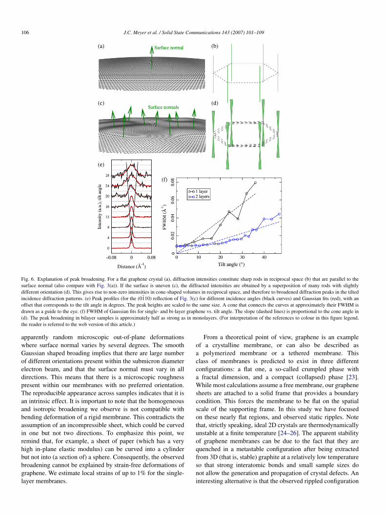
membrane as a number of locally flat pieces with slightly differ-ent orientations, each piece yields a diffraction peak at a slightlydifferent position, and their incoherent superposition leads todiffraction intensities that do not fall onto a single point. Inthe reciprocal space, this can be understood as a superpositionof rods with slightly different orientations (Fig. 6), so that thediffraction intensities are different from zero in a cone-shaped
volume. This model also predicts that the peaks are sharp at nor-mal incidence and their width increases linearly with tilt angle,as indeed observed experimentally. Fig. 6(f) shows the FWHMwidth of diffraction peaks with tilt angle. The linear slope canbe directly related to the cone angle, which is found to be ≈10◦
in monolayer samples. This means the surface normals deviateby ca. 5◦ from the mean surface. For bilayer membranes, thespot broadening is approximately half as strong as in monolay-ers, which implies a mean deviation of ≈2◦.
Although in bilayer samples the curvature of the membraneis only approximately half as strong as compared tomonolayers, it is easier to visualize directly. We could observethe roughness of bi-layer membranes by using the strongvariation in their diffraction intensities with tilt angle (Fig. 4(g),(h)). We used convergent beam electron diffraction (CBED)with the sample offset from the beam focus to map out thediffraction intensities for a portion of the sample (Fig. 7).In this way, each diffraction spot allowed us to image theilluminated area for this particular Bragg reflection [20]. Sincethese intensities are obtained through Bragg reflections fromthe crystal lattice, they depend only on the local orientation ofthe graphene membrane and cannot be an image of adsorbatesor defects. The variation of the incident beam angle across thesample due to the convergent probe can be neglected for a two-layer graphene membrane.1 The resolution is approximatelygiven by the size of the spot at the beam focus in Fig. 7(d).Reducing the spot size leads to strongly decreased diffractedintensities as compared to the undiffracted beam, whicheffectively limits the resolution (this can be seen by comparingFig. 7(f), that exhibits a good signal-to-noise ratio but showsonly large scale variations, with Fig. 7(g)–(j), in which the spotsize is optimized to obtain a better resolution at the expenseof a noisier signal). The variation in local orientation of themembrane leads to intensity variations within the CBED spotswhich is in agreement with the ca. ±2◦ deviation from theaverage normal that was inferred from the broadening of thespots in the nanoarea diffraction patterns. Fig. 7(g)–(j) showripples with a lateral extent down to 15 nm, which we estimateas the resolution limit in this configuration. Ripples of smallerlateral extent (few nm) have been observed by atomic resolutionTEM imaging [22]. Importantly, the ripples are found static(CBED patterns are reproduced at subsequent exposures, seeFig. 7) and have an apparently random distribution of lateralsizes, orientation and heights. We note again that the greyscales in Fig. 7(g)–(j) correspond to different orientations ratherthan heights: one can view the image in Fig. 7(h) as a curvedlandscape illuminated at a grazing angle from the lower leftcorner, like mountains at sunrise. The actual shapes of theripples become clear in this way; this appearance is welljustified by the underlying contrast mechanism.
Our TEM studies show that the suspended graphenemembranes assume a static, nonflat configuration with
106 J.C. Meyer et al. / Solid State Communications 143 (2007) 101–109
Fig. 6. Explanation of peak broadening. For a flat graphene crystal (a), diffraction intensities constitute sharp rods in reciprocal space (b) that are parallel to thesurface normal (also compare with Fig. 3(a)). If the surface is uneven (c), the diffracted intensities are obtained by a superposition of many rods with slightlydifferent orientation (d). This gives rise to non-zero intensities in cone-shaped volumes in reciprocal space, and therefore to broadened diffraction peaks in the tiltedincidence diffraction patterns. (e) Peak profiles (for the (0110) reflection of Fig. 3(c) for different incidence angles (black curves) and Gaussian fits (red), with anoffset that corresponds to the tilt angle in degrees. The peak heights are scaled to the same size. A cone that connects the curves at approximately their FWHM isdrawn as a guide to the eye. (f) FWHM of Gaussian fits for single- and bi-layer graphene vs. tilt angle. The slope (dashed lines) is proportional to the cone angle in(d). The peak broadening in bilayer samples is approximately half as strong as in monolayers. (For interpretation of the references to colour in this figure legend,the reader is referred to the web version of this article.)
apparently random microscopic out-of-plane deformationswhere surface normal varies by several degrees. The smoothGaussian shaped broading implies that there are large numberof different orientations present within the submicron diameterelectron beam, and that the surface normal must vary in alldirections. This means that there is a microscopic roughnesspresent within our membranes with no preferred orientation.The reproducible appearance across samples indicates that it isan intrinsic effect. It is important to note that the homogeneousand isotropic broadening we observe is not compatible withbending deformation of a rigid membrane. This contradicts theassumption of an incompressible sheet, which could be curvedin one but not two directions. To emphasize this point, weremind that, for example, a sheet of paper (which has a veryhigh in-plane elastic modulus) can be curved into a cylinderbut not into (a section of) a sphere. Consequently, the observedbroadening cannot be explained by strain-free deformations ofgraphene. We estimate local strains of up to 1% for the single-layer membranes.
From a theoretical point of view, graphene is an exampleof a crystalline membrane, or can also be described asa polymerized membrane or a tethered membrane. Thisclass of membranes is predicted to exist in three differentconfigurations: a flat one, a so-called crumpled phase witha fractal dimension, and a compact (collapsed) phase [23].While most calculations assume a free membrane, our graphenesheets are attached to a solid frame that provides a boundarycondition. This forces the membrane to be flat on the spatialscale of the supporting frame. In this study we have focusedon these nearly flat regions, and observed static ripples. Notethat, strictly speaking, ideal 2D crystals are thermodynamicallyunstable at a finite temperature [24–26]. The apparent stabilityof graphene membranes can be due to the fact that they arequenched in a metastable configuration after being extractedfrom 3D (that is, stable) graphite at a relatively low temperatureso that strong interatomic bonds and small sample sizes donot allow the generation and propagation of crystal defects. Aninteresting alternative is that the observed rippled configuration
J.C. Meyer et al. / Solid State Communications 143 (2007) 101–109 107
Fig. 7. Convergent-beam electron diffraction (CBED) patterns from a two-layer graphene membrane. With the probe beam focused on the membrane (a), a patternwith smooth intensity discs ((b), (c)) is obtained. If the sample is above (or below) the focus of the beam (d), each diffraction spot provides a mapping of thediffracted intensity for the illuminated area ((e), (f)). Variations in the local orientation of the membrane translate into intensity variations inside the diffractionspots. The resolution is limited by the spot width at the crossover (indicated by the black arrow in (d), idealized as a point in the diagram). Repeated exposures ofthe same area reproduce the same pattern ((g), (h)) but changing the position on the membrane shows a new configuration ((i), (j)). The illuminated area in (g)–(j)has a diameter of ca. 150 nm, and ripples with a lateral extent down to the resolution limit of 15 nm are visible. (k) Colour-coded CBED intensities, representing asample area of ca. 300 nm within the dashed line.
108 J.C. Meyer et al. / Solid State Communications 143 (2007) 101–109
Fig. 8. Non-flat graphene configurations. (a) Overview of a folded flake that does not bridge the gap in the supporting grid but is attached only at one side. (b), (c),(d) Close-ups that resolve individual layers. (c) Transition from a single folded area (two layers) to a double fold (four layers). (d) Graphene sheet folded back ontoitself and orientated parallel to the beam. The folding contains a hollow channel, similar in appearance and diameter to that typical for carbon nanotubes. We believethat similar nanoscrolls occur at the edges of flat areas such as shown in Fig. 4(e), (f). (e) Diffraction pattern from a scroll, and (f) the same pattern with featuresbeing assigned. The pattern is very similar to that of multiwalled carbon nanotubes. The dashed hexagons indicate two strong sets of peaks, showing that this scrollis rolled up almost along an armchair direction. The spacing and sharpness of (0002) type reflections shows that it is a tight scroll with an interlayer distance as inMWNTs (within experimental error). The streaks (indicated by arrows) show that the graphene sheet is indeed curved at the scrolls, rather than multiply folded.Scale bars (a) 50 nm, (b), (c), (d) 2 nm.
can increase the thermodynamic stability of (possibly strained)graphene membranes, and may in fact be energetically morefavourable [24–26]. While graphene on a substrate is supportedon the entire area, the membranes have a higher degree offreedom that would allow them to move towards a morefavoured configuration as far as permitted by the supportingframe that may also enforce a particular distribution of ripples.In fact, we also observed crumpled sheets that became partlydetached from the metal grid (Fig. 8), and we expect that further
studies of these structures, as well as of scrolled and foldedregions near membrane edges, will provide further insights intothe interesting problem of stability of 2D crystal systems. Inany case, more experimental and theoretical work is required tounderstand the observed roughness.
In conclusion, single-layer graphene can be used to make thethinnest possible membranes, with a thickness of just one atom.We present an unambiguous identification of single- and bi-layer samples by nanoarea electron diffraction. The membranes
J.C. Meyer et al. / Solid State Communications 143 (2007) 101–109 109
are not flat but exhibit random out of plane deformations. Theone atom thick membranes are intriguing objects for researchthat are strikingly different from ordinary three-dimensionalcrystals.
Acknowledgements
This work was supported in part by the Director, Office ofEnergy Research, Office of Basic Energy Sciences, MaterialsSciences Division of the US Department of Energy underContract No. DE-AC-03-76SF00098 and by the NationalScience Foundation under Grant No. EEC-0435914, supportingthe Centre of Integrated Nanomechanical Systems, theEU project CANAPE, the EPSRC (UK) and the RoyalSociety. M.I.K. acknowledges financial support from FOM(Netherlands).
References
[1] K.S. Novoselov, et al., Electric field effect in atomically thin carbon films,Science 306 (2004) 666–669.
[2] K.S. Novoselov, et al., Two-dimensional atomic crystals, Proc. Natl Acad.Sci. USA 102 (2005) 10451–10453.
[3] K.S. Novoselov, et al., Two-dimensional gas of massless Dirac fermionsin graphene, Nature 438 (2005) 197–200.
[4] Y. Zhang, J.W. Tan, H.L. Stormer, P. Kim, Experimental observation ofthe quantum Hall effect and Berry’s phase in graphene, Nature 438 (2005)201–204.
[5] A.C. Ferrari, et al., The Raman spectrum of graphene and graphene layers,Phys. Rev. Lett. 97 (2006) 187401.
[6] A. Gupta, et al., Raman scattering from high-frequency phonons insupported n-graphene layer films, Nano Lett. 6 (2006) 2667–2673.
[7] D. Graf, et al., Spatially resolved Raman spectroscopy of single- and few-layer graphene, Nano Lett. 7 (2007) 238–242.
[8] J.S. Bunch, et al., Electromechanical resonators from graphene sheets,Science 315 (2007) 490–493.
[10] R.E. Peierls, Quelques proprietes typiques des corpses solides, Ann. Inst.H. Poincare 5 (1935) 177–222.
[11] L.D. Landau, Zur theorie der phasenumwandlungen II, Phys. Z.Sowjetunion 11 (1937) 26–35.
[12] L.D. Landau, E.M. Lifshitz, Statistical Physics, Part I, Pergamon Press,Oxford, 1980.
[13] N.D. Mermin, H. Wagner, Absence of ferromagnetism or antiferromag-netism in one- or two-dimensional isotropic Heisenberg models, Phys.Rev. Lett. 17 (1966) 1133–1136.
[14] N.D. Mermin, Crystalline order in two dimensions, Phys. Rev. 176 (1968)250–254.
[15] J.C. Meyer, et al., Single molecule torsional pendulum, Science 309(2005) 1539–1541.
[16] J.C. Meyer, et al., Electron diffraction analysis of individual single-walledcarbon nanotubes, Ultramicroscopy 106 (2006) 176–190.
[17] D.K. Bhattacharya, et al., Japan. J. Appl. Phys. 36 (1997) 2918–2921.[18] P.A. Doyle, P.S. Turner, Relativistic Hartree–Fock x-ray and electron
scattering factors, Acta Crystallogr. A 24 (1968) 390–397.[19] S. Horiuchi, et al., Carbon nanofilm with a new structure and property,
Japan. J. Appl. Phys. 42 (2003) L1073–L1076.[20] P.R. Buseck, J.M. Cowley, L. Eyring, High-Resolution Transmission
Electron Microscopy, Oxford University Press, 1988.[21] J.C.H. Spence, High-Resolution Electron Microscopy, Oxford University
Press, 2003.[22] J.C. Meyer, et al., The structure of suspended graphene sheets, Nature
(March 1) (2007).[23] G. Gompper, D.M. Kroll, Network models of fluid, hexatic and
polymerized membranes, J. Phys. Condens. Matter 9 (1997) 8795–8834.[24] D.R. Nelson, L. Peliti, Fluctuations in membranes with crystalline and
hexatic order, J. Physique 48 (1987) 1085–1092.[25] L. Radzihovsky, P. Le Doussal, Self-consistent theory of polymerized
membranes, Phys. Rev. Lett. 69 (1992) 1209–1212.[26] D.R. Nelson, T. Piran, S. Weinberg, Statistical Mechanics of Membranes


![Suppression of intrinsic roughness in encapsulated graphene · tilt analysis in the transmission electron microscope (TEM) [2,20]. In contrast to scanning probe techniques, this method](https://static.documents.pub/doc/80x56/5f3ed37e48dd6e68c82ac328/suppression-of-intrinsic-roughness-in-encapsulated-graphene-tilt-analysis-in-the.jpg)


