LMP7717/LMP771888 MHz, Precision, Low Noise, 1.8V CMOS Input,Decompensated Operational AmplifierGeneral DescriptionThe LMP7717 (single) and the LMP7718 (dual) low noise,CMOS input operational amplifiers offer a low input voltagenoise density of 5.8 nV/ while consuming only 1.15 mA(LMP7717) of quiescent current. The LMP7717/LMP7718 arestable at a gain of 10 and have a gain bandwidth (GBW)product of 88 MHz. The LMP7717/LMP7718 have a supplyvoltage range of 1.8V to 5.5V and can operate from a singlesupply. The LMP7717/LMP7718 each feature a rail-to-railoutput stage. Both amplifiers are part of the LMP® precisionamplifier family and are ideal for a variety of instrumentationapplications.
The LMP7717 family provides optimal performance in lowvoltage and low noise systems. A CMOS input stage, withtypical input bias currents in the range of a few femto-Am-peres, and an input common mode voltage range, whichincludes ground, make the LMP7717/LMP7718 ideal for lowpower sensor applications where high speeds are needed.
The LMP7717/LMP7718 are manufactured using National’sadvanced VIP50 process. The LMP7717 is offered in either a5-Pin SOT23 or an 8-Pin SOIC package. The LMP7718 isoffered in either the 8-Pin SOIC or the 8-Pin MSOP.
If Military/Aerospace specified devices are required,please contact the National Semiconductor Sales Office/Distributors for availability and specifications.
ESD Tolerance (Note 2)
Human Body Model 2000V
Machine Model 200V
VIN Differential ±0.3V
Supply Voltage (V+ – V−) 6.0V
Input/Output Pin Voltage V+ +0.3V, V− −0.3V
Storage Temperature Range −65°C to 150°C
Junction Temperature (Note 3) +150°C
Soldering Information
Infrared or Convection (20 sec) 235°C
Wave Soldering Lead Temp (10 sec) 260°C
Operating Ratings (Note 1)
Temperature Range (Note 3) −40°C to 125°C
Supply Voltage (V+ – V−)
−40°C ≤ TA ≤ 125°C 2.0V to 5.5V
0°C ≤ TA ≤ 125°C 1.8V to 5.5V
Package Thermal Resistance (θJA (Note 3))
5-Pin SOT23 180°C/W
8-Pin SOIC 190°C/W
8-Pin MSOP 236°C/W
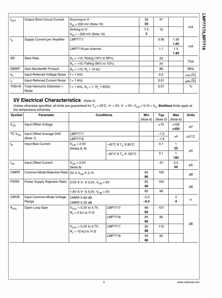
2.5V Electrical Characteristics (Note 4)
Unless otherwise specified, all limits are guaranteed for TA = 25°C, V+ = 2.5V, V− = 0V, VCM = V+/2 = VO. Boldface limits apply atthe temperature extremes.
Symbol Parameter Conditions Min
(Note 6)
Typ
(Note 5)
Max
(Note 6)
Units
VOS Input Offset Voltage ±20 ±180
±480µV
TC VOS Input Offset Average Drift
(Note 7)
LMP7717 −1.0±4 μV/°C
LMP7718 −1.8
IB Input Bias Current VCM = 1.0V
(Notes 8, 9)−40°C ≤ TA ≤ 85°C 0.05 1
25pA
−40°C ≤ TA ≤ 125°C 0.05 1
100
IOS Input Offset Current VCM = 1.0V
(Note 9)
.006 0.5
50pA
CMRR Common Mode Rejection Ratio 0V ≤ VCM ≤ 1.4V 83
80
94 dB
PSRR Power Supply Rejection Ratio 2.0V ≤ V+ ≤ 5.5V, VCM = 0V 85
80
100
dB
1.8V ≤ V+ ≤ 5.5V, VCM = 0V 85 98
CMVR Input Common-Mode Voltage
RangeCMRR ≥ 60 dB
CMRR ≥ 55 dB
−0.3
−0.3
1.5
1.5 V
AVOL Open Loop Gain VOUT = 0.15V to 2.2V,
RL = 2 kΩ to V+/2
LMP7717 88
82
98
dB
LMP7718 84
80
92
VOUT = 0.15V to 2.2V,
RL = 10 kΩ to V+/2
LMP7717 92
88
110
LMP7718 90
86
95
VOUT Output Swing High RL = 2 kΩ to V+/2 25 70
77
mV from
rail
RL = 10 kΩ to V+/2 20 60
66
Output Swing Low RL = 2 kΩ to V+/2 30 70
73
RL = 10 kΩ to V+/2 15 60
62
www.national.com 2
LM
P7717/L
MP
7718
IOUT Output Short Circuit Current Sourcing to V−
VIN = 200 mV (Note 10)
36
30
47
mASinking to V+
VIN = –200 mV (Note 10)
7.5
5
15
IS Supply Current per Amplifier LMP7717 0.95 1.30
1.65mA
LMP7718 per channel 1.1 1.5
1.85
SR Slew Rate AV = +10, Rising (10% to 90%) 32 V/μs
AV = +10, Falling (90% to 10%) 24
GBWP Gain Bandwidth Product AV = +10, RL = 10 kΩ 88 MHz
en Input-Referred Voltage Noise f = 1 kHz 6.2 nV/
in Input-Referred Current Noise f = 1 kHz 0.01 pA/
THD+N Total Harmonic Distortion +
Noisef = 1 kHz, AV = 1, RL = 600Ω 0.01 %
5V Electrical Characteristics (Note 4)
Unless otherwise specified, all limits are guaranteed for TA = 25°C, V+ = 5V, V− = 0V, VCM = V+/2 = VO. Boldface limits apply atthe temperature extremes.
Symbol Parameter Conditions Min
(Note 6)
Typ
(Note 5)
Max
(Note 6)
Units
VOS Input Offset Voltage ±10 ±150
±450µV
TC VOS Input Offset Average Drift
(Note 7)
LMP7717 −1.0±4 μV/°C
LMP7718 −1.8
IB Input Bias Current VCM = 2.0V
(Notes 8, 9)−40°C ≤ TA ≤ 85°C 0.1 1
25pA
−40°C ≤ TA ≤ 125°C 0.1 1
100
IOS Input Offset Current VCM = 2.0V
(Note 9)
.01 0.5
50pA
CMRR Common Mode Rejection Ratio 0V ≤ VCM ≤ 3.7V 85
80
100 dB
PSRR Power Supply Rejection Ratio 2.0V ≤ V+ ≤ 5.5V, VCM = 0V 85
80
100
dB
1.8V ≤ V+ ≤ 5.5V, VCM = 0V 85 98
CMVR Input Common-Mode Voltage
RangeCMRR ≥ 60 dB
CMRR ≥ 55 dB
−0.3
−0.3
4
4 V
AVOL Open Loop Gain VOUT = 0.3V to 4.7V,
RL = 2 kΩ to V+/2
LMP7717 88
82
107
dB
LMP7718 84
80
90
VOUT = 0.3V to 4.7V,
RL = 10 kΩ to V+/2
LMP7717 92
88
110
LMP7718 90
86
95
3 www.national.com
LM
P7717/L
MP
7718
VOUT Output Swing High RL = 2 kΩ to V+/2 LMP7717 35 70
77
mV from
rail
LMP7718 45 80
77
RL = 10 kΩ to V+/2 25 60
66
Output Swing Low RL = 2 kΩ to V+/2 LMP7717 42 70
73
LMP7718 50 80
78
RL = 10 kΩ to V+/2 25 60
66
IOUT Output Short Circuit Current Sourcing to V−
VIN = 200 mV (Note 10)
46
38
60
mASinking to V+
VIN = –200 mV (Note 10)
10.5
6.5
21
IS Supply Current per Amplifier LMP7717 1.15 1.40
1.75mA
LMP7718 per channel 1.30 1.70
2.05
SR Slew Rate AV = +10, Rising (10% to 90%) 35 V/μs
AV = +10, Falling (90% to 10%) 28
GBWP Gain Bandwidth Product AV = +10, RL = 10 kΩ 88 MHz
en Input-Referred Voltage Noise f = 1 kHz 5.8 nV/
in Input-Referred Current Noise f = 1 kHz 0.01 pA/
THD+N Total Harmonic Distortion +
Noisef = 1 kHz, AV = 1, RL = 600Ω 0.01 %
Note 1: Absolute Maximum Ratings indicate limits beyond which damage to the device may occur. Operating Ratings indicate conditions for which the device isintended to be functional, but specific performance is not guaranteed. For guaranteed specifications and the test conditions, see the Electrical CharacteristicsTables.
Note 2: Human Body Model, applicable std. MIL-STD-883, Method 3015.7. Machine Model, applicable std. JESD22-A115-A (ESD MM std. of JEDEC)
Note 3: The maximum power dissipation is a function of TJ(MAX), θJA. The maximum allowable power dissipation at any ambient temperature isPD = (TJ(MAX) - TA)/θJA. All numbers apply for packages soldered directly onto a PC Board.
Note 4: Electrical Table values apply only for factory testing conditions at the temperature indicated. Factory testing conditions result in very limited self-heatingof the device such that TJ = TA. No guarantee of parametric performance is indicated in the electrical tables under conditions of internal self-heating where TJ >TA.
Note 5: Typical values represent the most likely parametric norm as determined at the time of characterization. Actual typical values may vary over time and willalso depend on the application and configuration. The typical values are not tested and are not guaranteed on shipped production material.
Note 6: Limits are 100% production tested at 25°C. Limits over the operating temperature range are guaranteed through correlations using the statistical qualitycontrol (SQC) method.
Note 7: Offset voltage average drift is determined by dividing the change in VOS by temperature change.
Note 8: Positive current corresponds to current flowing into the device.
Note 9: Input bias current and input offset current are guaranteed by design
Note 10: The short circuit test is a momentary test, the short circuit duration is 1.5 ms.
www.national.com 4
LM
P7717/L
MP
7718
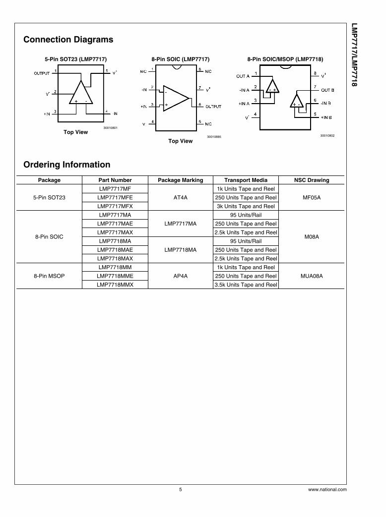
Connection Diagrams
5-Pin SOT23 (LMP7717)
30010801
Top View
8-Pin SOIC (LMP7717)
30010885
Top View
8-Pin SOIC/MSOP (LMP7718)
30010802
Ordering Information
Package Part Number Package Marking Transport Media NSC Drawing
The LMP7717/LMP7718 are high performance op amps thatprovide a GBW of 88 MHz with a gain of 10 while drawing alow supply current of 1.15 mA. This makes them ideal for pro-viding wideband amplification in data acquisition applications.
With the proper external compensation the LMP7717 can beoperated at gains of ±1 and still maintain much faster slewrates than comparable unity gain stable amplifiers. The in-crease in bandwidth and slew rate is obtained without anyadditional power consumption over the LMP7715.
Low Input Referred Noise and Low Input Bias Current
The LMP7717/LMP7718 have a very low input referred volt-age noise density (5.8 nV/ at 1 kHz). A CMOS input stageensures a small input bias current (100 fA) and low input re-ferred current noise (0.01 pA/ ). This is very helpful inmaintaining signal integrity, and makes the LMP7717/LMP7718 ideal for audio and sensor based applications.
Low Supply Voltage
The LMP7717 and the LMP7718 have performance guaran-teed at 2.5V and 5V supply. These parts are guaranteed tobe operational at all supply voltages between 2.0V and 5.5V,for ambient temperatures ranging from −40°C to 125°C, thusutilizing the entire battery lifetime. The LMP7717/LMP7718are also guaranteed to be operational at 1.8V supply voltage,for temperatures between 0°C and 125°C optimizing their us-age in low-voltage applications.
RRO and Ground Sensing
Rail-to-Rail output swing provides the maximum possible dy-namic range. This is particularly important when operating atlow supply voltages. An innovative positive feedback schemeis used to boost the current drive capability of the outputstage. This allows the LMP7717/LMP7718 to source morethan 40 mA of current at 1.8V supply. This also limits the per-formance of the these parts as comparators, and hence theusage of the LMP7717 and the LMP7718 in an open-loopconfiguration is not recommended. The input common-moderange includes the negative supply rail which allows directsensing at ground in single supply operation.
Small Size
The small footprints of the LMP7717 packages and theLMP7718 packages save space on printed circuit boards, andenable the design of smaller electronic products, such as cel-lular phones, pagers, or other portable systems. Long tracesbetween the signal source and the op amp make the signalpath more susceptible to noise pick up.
The physically smaller LMP7717 or LMP7718 packages allowthe op amp to be placed closer to the signal source, thus re-ducing noise pickup and maintaining signal integrity.
USING THE DECOMPENSATED LMP7717
Advantages of Decompensated Op Amp
A unity gain stable op amp, which is fully compensated, isdesigned to operate with good stability down to gains of ±1.The large amount of compensation does provide an op ampthat is relatively easy to use; however, a decompensated opamp is designed to maximize the bandwidth and slew ratewithout any additional power consumption. This can be veryadvantageous.
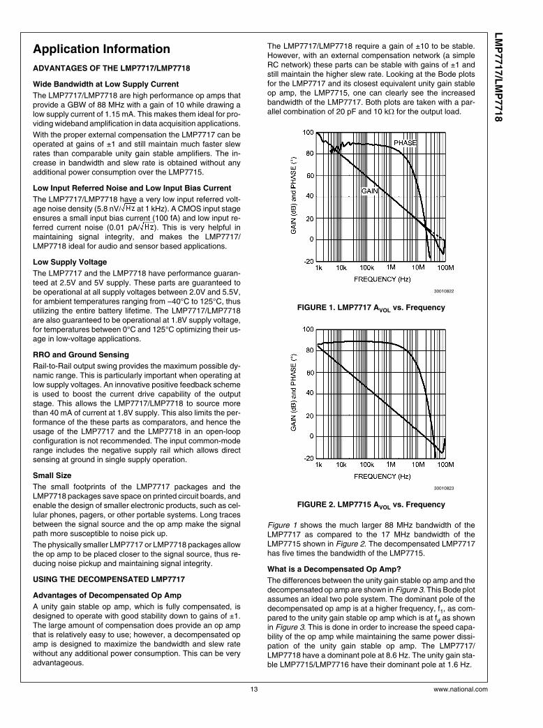
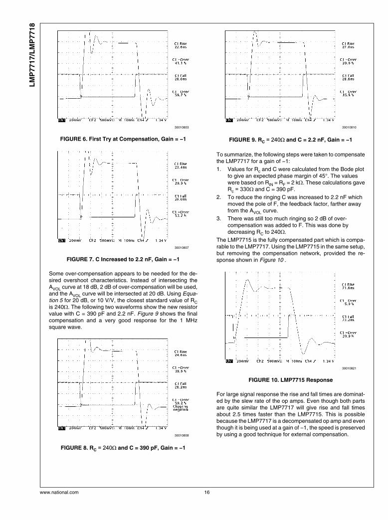
The LMP7717/LMP7718 require a gain of ±10 to be stable.However, with an external compensation network (a simpleRC network) these parts can be stable with gains of ±1 andstill maintain the higher slew rate. Looking at the Bode plotsfor the LMP7717 and its closest equivalent unity gain stableop amp, the LMP7715, one can clearly see the increasedbandwidth of the LMP7717. Both plots are taken with a par-allel combination of 20 pF and 10 kΩ for the output load.
30010822
FIGURE 1. LMP7717 AVOL vs. Frequency
30010823
FIGURE 2. LMP7715 AVOL vs. Frequency
Figure 1 shows the much larger 88 MHz bandwidth of theLMP7717 as compared to the 17 MHz bandwidth of theLMP7715 shown in Figure 2. The decompensated LMP7717has five times the bandwidth of the LMP7715.
What is a Decompensated Op Amp?
The differences between the unity gain stable op amp and thedecompensated op amp are shown in Figure 3. This Bode plotassumes an ideal two pole system. The dominant pole of thedecompensated op amp is at a higher frequency, f1, as com-pared to the unity gain stable op amp which is at fd as shownin Figure 3. This is done in order to increase the speed capa-bility of the op amp while maintaining the same power dissi-pation of the unity gain stable op amp. The LMP7717/LMP7718 have a dominant pole at 8.6 Hz. The unity gain sta-ble LMP7715/LMP7716 have their dominant pole at 1.6 Hz.
13 www.national.com
LM
P7717/L
MP
7718
30010824
FIGURE 3. Open Loop Gain for Unity Gain Stable Op Ampand Decompensated Op Amp
Having a higher frequency for the dominate pole will result in:
1. The DC open loop gain (AVOL) extending to a higherfrequency.
2. A wider closed loop bandwidth.
3. Better slew rate due to reduced compensationcapacitance within the op amp.
The second open loop pole (f2) for the LMP7717/LMP7718occurs at 45 MHz. The unity gain (fu’) occurs after the secondpole at 51 MHz. An ideal two pole system would give a phasemargin of 45° at the location of the second pole. TheLMP7717/LMP7718 have parasitic poles close to the secondpole, giving a phase margin closer to 0°. Therefore it is nec-essary to operate the LMP7717/LMP7718 at a closed loopgain of 10 or higher, or to add external compensation in orderto assure stability.
For the LMP7715, the gain bandwidth product occurs at 17MHz. The curve is constant from fd to fu which occurs beforethe second pole.
For the LMP7717/LMP7718 the GBW = 88 MHz and is con-stant between f1 and f2. The second pole at f2 occurs beforeAVOL =1. Therefore fu’ occurs at 51 MHz, well before the GBWfrequency of 88 MHz. For decompensated op amps the unitygain frequency and the GBW are no longer equal. Gmin is theminimum gain for stability and for the LMP7717/LMP7718 thisis a gain of 10 or 20 dB.
Input Lead-Lag Compensation
The recommended technique which allows the user to com-pensate the LMP7717/LMP7718 for stable operation at anygain is lead-lag compensation. The compensation compo-nents added to the circuit allow the user to shape the feedbackfunction to make sure there is sufficient phase margin whenthe loop gain is as low as 0 dB and still maintain the advan-tages over the unity gain op amp. Figure 4 shows the lead-lag configuration. Only RC and C are added for the necessarycompensation.
30010825
FIGURE 4. LMP7717 with Lead-Lag Compensation forInverting Configuration
To cover how to calculate the compensation network valuesit is necessary to introduce the term called the feedback factoror F. The feedback factor F is the feedback voltage VA-VBacross the op amp input terminals relative to the op amp out-put voltage VOUT.
From feedback theory the classic form of the feedback equa-tion for op amps is:
A is the open loop gain of the amplifier and AF is the loop gain.Both are highly important in analyzing op amps. Normally AF>>1 and so the above equation reduces to:
Deriving the equations for the lead-lag compensation is be-yond the scope of this datasheet. The derivation is based onthe feedback equations that have just been covered. The in-verse of feedback factor for the circuit in Figure 4 is:
(1)
where 1/F's pole is located at
(2)
1/F's zero is located at
(3)
www.national.com 14
LM
P7717/L
MP
7718
(4)
The circuit gain for Figure 4 at low frequencies is −RF/RIN, butF, the feedback factor is not equal to the circuit gain. Thefeedback factor is derived from feedback theory and is thesame for both inverting and non-inverting configurations. Yes,the feedback factor at low frequencies is equal to the gain forthe non-inverting configuration.
(5)
From this formula, we can see that
• 1/F's zero is located at a lower frequency compared with1/F's pole.
• 1/F's value at low frequency is 1 + RF/RIN.
• This method creates one additional pole and oneadditional zero.
• This pole-zero pair will serve two purposes:
— To raise the 1/F value at higher frequencies prior to itsintercept with A, the open loop gain curve, in order tomeet the Gmin = 10 requirement. For the LMP7717some overcompensation will be necessary for goodstability.
— To achieve the previous purpose above with noadditional loop phase delay.
Please note the constraint 1/F ≥ Gmin needs to be satisfiedonly in the vicinity where the open loop gain A and 1/F inter-sect; 1/F can be shaped elsewhere as needed. The 1/F polemust occur before the intersection with the open loop gain A.
In order to have adequate phase margin, it is desirable to fol-low these two rules:
Rule 1 1/F and the open loop gain A should intersect at thefrequency where there is a minimum of 45° of phasemargin. When over-compensation is required the in-tersection point of A and 1/F is set at a frequencywhere the phase margin is above 45°, therefore in-creasing the stability of the circuit.
Rule 2 1/F’s pole should be set at least one decade belowthe intersection with the open loop gain A in order totake advantage of the full 90° of phase lead broughtby 1/F’s pole which is F’s zero. This ensures that theeffect of the zero is fully neutralized when the 1/F andA plots intersect each other.
Calculating Lead-Lag Compensation for LMP7717
Figure 5 is the same plot as Figure 1, but the AVOL and phasecurves have been redrawn as smooth lines to more readilyshow the concepts covered, and to clearly show the key pa-rameters used in the calculations for lead-lag compensation.
30010848
FIGURE 5. LMP7717/LMP7718 Simplified Bode Plot
To obtain stable operation with gains under 10 V/V the openloop gain margin must be reduced at high frequencies towhere there is a 45° phase margin when the gain margin ofthe circuit with the external compensation is 0 dB. The poleand zero in F, the feedback factor, control the gain margin atthe higher frequencies. The distance between F and AVOL isthe gain margin; therefore, the unity gain point (0 dB) is whereF crosses the AVOL curve.
For the example being used RIN = RF for a gain of −1. There-fore F = 6 dB at low frequencies. At the higher frequenciesthe minimum value for F is 18 dB for 45° phase margin. FromEquation 5 we have the following relationship:
Now set RF = RIN = R. With these values and solving for RCwe have RC = R/5.9. Note that the value of C does not affectthe ratio between the resistors. Once the value of the resistorsis set, then the position of the pole in F must be set. A 2 kΩresistor is used for RF and RIN in this design. Therefore thevalue for RC is set at 330Ω, the closest standard value for 2kΩ/5.9.Rewriting Equation 2 to solve for the minimum capacitor valuegives the following equation:
C = 1/(2πfpRC)
The feedback factor curve, F, intersects the AVOL curve atabout 12 MHz. Therefore the pole of F should not be anylarger than 1.2 MHz. Using this value and RC = 330Ω theminimum value for C is 390 pF. Figure 6 shows that there istoo much overshoot, but the part is stable. Increasing C to 2.2nF did not improve the ringing, as shown in Figure 7.
15 www.national.com
LM
P7717/L
MP
7718
30010803
FIGURE 6. First Try at Compensation, Gain = −1
30010807
FIGURE 7. C Increased to 2.2 nF, Gain = −1
Some over-compensation appears to be needed for the de-sired overshoot characteristics. Instead of intersecting theAVOL curve at 18 dB, 2 dB of over-compensation will be used,and the AVOL curve will be intersected at 20 dB. Using Equa-tion 5 for 20 dB, or 10 V/V, the closest standard value of RCis 240Ω. The following two waveforms show the new resistorvalue with C = 390 pF and 2.2 nF. Figure 9 shows the finalcompensation and a very good response for the 1 MHzsquare wave.
30010808
FIGURE 8. RC = 240Ω and C = 390 pF, Gain = −1
30010810
FIGURE 9. RC = 240Ω and C = 2.2 nF, Gain = −1
To summarize, the following steps were taken to compensatethe LMP7717 for a gain of −1:
1. Values for Rc and C were calculated from the Bode plotto give an expected phase margin of 45°. The valueswere based on RIN = RF = 2 kΩ. These calculations gaveRc = 330Ω and C = 390 pF.
2. To reduce the ringing C was increased to 2.2 nF whichmoved the pole of F, the feedback factor, farther awayfrom the AVOL curve.
3. There was still too much ringing so 2 dB of over-compensation was added to F. This was done bydecreasing RC to 240Ω.
The LMP7715 is the fully compensated part which is compa-rable to the LMP7717. Using the LMP7715 in the same setup,but removing the compensation network, provided the re-sponse shown in Figure 10 .
30010821
FIGURE 10. LMP7715 Response
For large signal response the rise and fall times are dominat-ed by the slew rate of the op amps. Even though both partsare quite similar the LMP7717 will give rise and fall timesabout 2.5 times faster than the LMP7715. This is possiblebecause the LMP7717 is a decompensated op amp and eventhough it is being used at a gain of −1, the speed is preservedby using a good technique for external compensation.
www.national.com 16
LM
P7717/L
MP
7718
Non-Inverting Compensation
For the non-inverting amp the same theory applies for estab-lishing the needed compensation. When setting the invertingconfiguration for a gain of −1, F has a value of 2. For the non-inverting configuration both F and the actual gain are thesame, making the non-inverting configuration more difficult tocompensate. Using the same circuit as shown in Figure 4, butsetting up the circuit for non-inverting operation (gain of +2)results in similar performance as the inverting configurationwith the inputs set to half the amplitude to compensate for theadditional gain. Figure 11 below shows the results.
30010882
FIGURE 11. RC = 240Ω and C = 2.2 nF, Gain = +2
30010883
FIGURE 12. LMP7715 Response Gain = +2
The response shown in Figure 11 is close to the responseshown in Figure 9. The part is actually slightly faster in thenon-inverting configuration. Decreasing the value of RC toaround 200Ω can decrease the negative overshoot but willhave slightly longer rise and fall times. The other option is toadd a small resistor in series with the input signal. Figure 12shows the performance of the LMP7715 with no compensa-tion. Again the decompensated parts are almost 2.5 timesfaster than the fully compensated op amp.
The most difficult op amp configuration to stabilize is the gainof +1. With proper compensation the LMP7717/LMP7718 canbe used in this configuration and still maintain higher speeds
than the fully compensated parts. Figure 13 shows the gain =1, or the buffer configuration, for these parts.
30010884
FIGURE 13. LMP7717 with Lead-Lag Compensation forNon-Inverting Configuration
Figure 13 is the result of using Equation 5 and additional ex-perimentation in the lab. RP is not part of Equation 5, but it isnecessary to introduce another pole at the input stage forgood performance at gain = +1. Equation 5 is shown belowwith RIN = ∞.
Using 2 kΩ for RF and solving for RC gives RC = 2000/6.9 =290Ω. The closest standard value for RC is 300Ω. After somefine tuning in the lab RC = 330Ω and RP = 1.5 kΩ were chosenas the optimum values. RP together with the input capacitanceat the non-inverting pin inserts another pole into the compen-sation for the LMP7717. Adding this pole and slightly reducingthe compensation for 1/F (using a slightly higher resistor valuefor RC) gives the optimum response for a gain of +1. Figure14 is the response of the circuit shown in Figure 13. Figure15 shows the response of the LMP7715 in the buffer config-uration with no compensation and RP = RF = 0.
30010888
FIGURE 14. RC = 330Ω and C = 10 nF, Gain = +1
17 www.national.com
LM
P7717/L
MP
7718
30010889
FIGURE 15. LMP7715 Response Gain = +1
With no increase in power consumption the decompensatedop amp offers faster speed than the compensated equivalentpart . These examples used RF = 2 kΩ. This value is highenough to be easily driven by the LMP7717/LMP7718, yetsmall enough to minimize the effects from the parasitic ca-pacitance of both the PCB and the op amp.
Note: When using the LMP7717/LMP7718, proper high fre-quency PCB layout must be followed. The GBW of these partsis 88 MHz, making the PCB layout significantly more criticalthan when using the compensated counterparts which havea GBW of 17 MHz.
TRANSIMPEDANCE AMPLIFIER
An excellent application for either the LMP7717 or theLMP7718 is as a transimpedance amplifier. With a GBWproduct of 88 MHz these parts are ideal for high speed datatransmission by light. The circuit shown on the front page ofthe datasheet is the circuit used to test theLMP7717/LMP7718 as transimpedance amplifiers. The onlychange is that VB is tied to the VCC of the part, thus the direc-tion of the diode is reversed from the circuit shown on the frontpage.
Very high speed components were used in testing to checkthe limits of the LMP7717/LMP7718 in a transimpedanceconfiguration. The photodiode part number is PIN-HR040from OSI Optoelectronics. The diode capacitance for this partis only about 7 pF for the 2.5V bias used (VCC to virtualground). The rise time for this diode is 1 nsec. A laser diodewas used for the light source. Laser diodes have on and offtimes under 5 nsec. The speed of the selected optical com-ponents allowed an accurate evaluation of the LMP7717 asa transimpedance amplifier. Nationals evaluation board fordecompensated op amps, PN 551013271-001 A, was usedand only minor modifications were necessary and no traceshad to be cut.
30010861
FIGURE 16. Transimpedance Amplifier
Figure 16 is the complete schematic for a transimpedanceamplifier. Only the supply bypass capacitors are not shown.CD represents the photodiode capacitance which is given onits datasheet. CCM is the input common mode capacitance ofthe op amp and, for the LMP7717 it is shown in the last graphof the Typical Performance Characteristics section of thisdatasheet. In Figure 16 the inverting input pin of the LMP7717is kept at virtual ground. Even though the diode is connectedto the 2.5V line, a power supply line is AC ground, thus CD isconnected to ground.
Figure 17 shows the schematic needed to derive F, the feed-back factor, for a transimpedance amplifier. In this figureCD + CCM = CIN. Therefore it is critical that the designer knowsthe diode capacitance and the op amp input capacitance. Thephotodiode is close to an ideal current source once its ca-pacitance is included in the model. What kind of circuit is this?Without CF there is only an input capacitor and a feedbackresistor. This circuit is a differentiator! Remember, differen-tiator circuits are inherently unstable and must be compen-sated. In this case CF compensates the circuit.
30010864
FIGURE 17. Transimpedance Feedback Model
www.national.com 18
LM
P7717/L
MP
7718
Using feedback theory, F = VA/VOUT, this becomes a voltagedivider giving the following equation:
The noise gain is 1/F. Because this is a differentiator circuit,a zero must be inserted. The location of the zero is given by:
CF has been added for stability. The addition of this part addsa pole to the circuit. The pole is located at:
To attain maximum bandwidth and still have good stability thepole is to be located on the open loop gain curve which is A.If additional compensation is required one can always in-crease the value of CF, but this will also reduce the bandwidthof the circuit. Therefore A = 1/F, or AF = 1. For A the equationis:
The expression fGBW is the gain bandwidth product of the part.For a unity gain stable part this is the frequency where A = 1.For the LMP7717 fGBW = 88 MHz. Multiplying A and F resultsin the following equation:
For the above equation s = jω. To find the actual amplitude ofthe equation the square root of the square of the real andimaginary parts are calculated. At the intersection of F and A,we have:
After a bit of algebraic manipulation the above equation re-duces to:
In the above equation the only unknown is CF. In trying tosolve this equation the fourth power of CF must be dealt with.An excel spread sheet with this equation can be used and allthe known values entered. Then through iteration, the valueof CF when both sides are equal will be found. That is thecorrect value for CF and of course the closest standard valueis used for CF.
Before moving to the lab, the transfer function of the tran-simpedance amplifier must be found and the units must be inOhms.
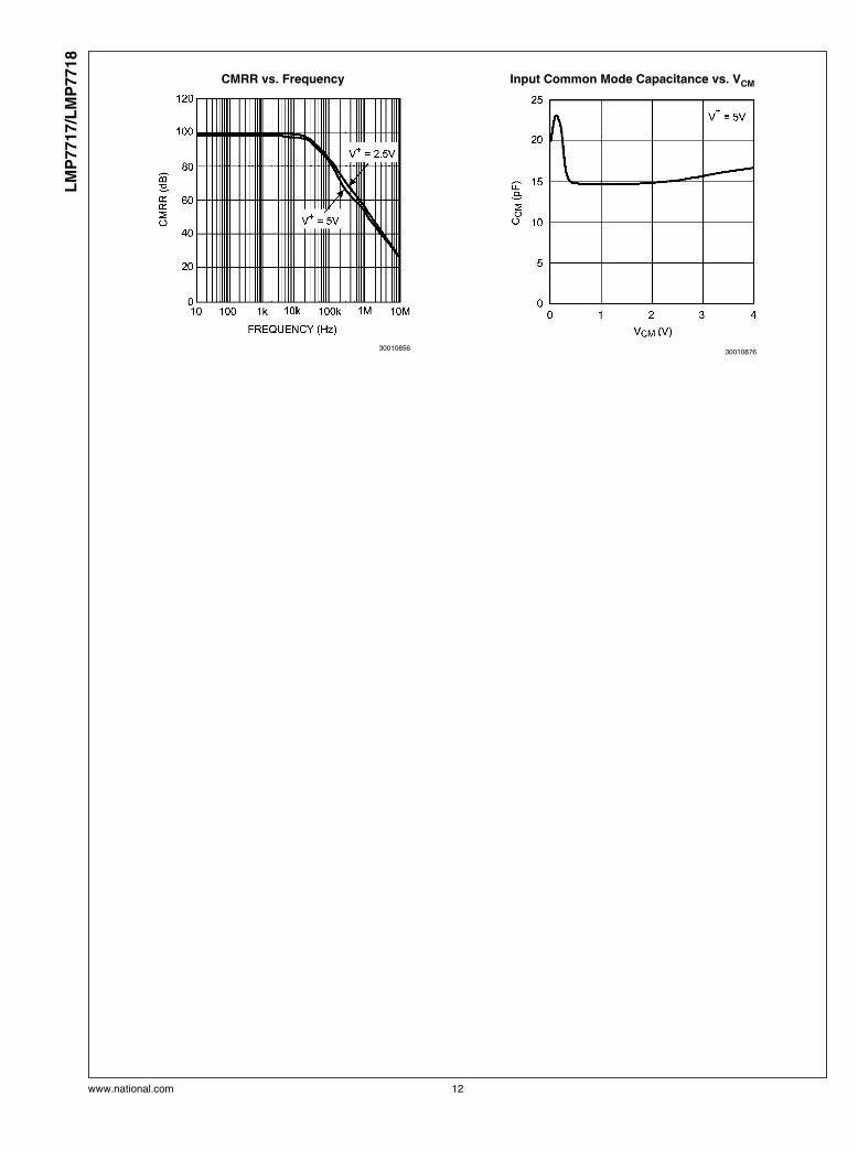
The LMP7717 was evaluated for RF = 10 kΩ and 100 kΩ,representing a somewhat lower gain configuration and withthe 100 kΩ feedback resistor a fairly high gain configuration.The RF = 10 kΩ is covered first. Looking at the Input CommonMode Capacitance vs. VCM chart for CCM for the operatingpoint selected CCM = 15 pF. Note that for split supplies VCM =2.5V, CIN = 22 pF and fGBW = 88 MHz. Solving for CF the cal-culated value is 1.75 pF, so 1.8 pF is selected for use.Checking the frequency of the pole finds that it is at 8.8 MHz,which is right at the minimum gain recommended for this part.Some over compensation was necessary for stability and thefinal selected value for CF is 2.7 pF. This moves the pole to5.9 MHz. Figure 18 and Figure 19 show the rise and fall timesobtained in the lab with a 1V output swing. The laser diodewas difficult to drive due to thermal effects making the startingand ending point of the pulse quite different, therefore the twoseparate scope pictures.
30010894
FIGURE 18. Fall Time
19 www.national.com
LM
P7717/L
MP
7718
30010895
FIGURE 19. Rise Time
In Figure 18 the ringing and the hump during the on time isfrom the laser. The higher drive levels for the laser gave ring-ing in the light source as well as light changing from thethermal characteristics. The hump is due to the thermal char-acteristics.
Solving for CF using a 100 kΩ feedback resistor, the calcu-lated value is 0.54 pF. One of the problems with more gain isthe very small value for CF. A 0.5 pF capacitor was used, itsmeasured value being 0.64 pF. For the 0.64 pF location the
pole is at 2.5 MHz. Figure 20 shows the response for a 1Voutput.
30010896
FIGURE 20. High Gain Response
A transimpedance amplifier is an excellent application for theLMP7717. Even with the high gain using a 100 kΩ feedbackresistor, the bandwidth is still well over 1 MHz. Other than alittle over compensation for the 10 kΩ feedback resistor con-figuration using the LMP7717 was quite easy. Of course avery good board layout was also used for this test.
Power Management www.national.com/power Feedback www.national.com/feedback
Switching Regulators www.national.com/switchers
LDOs www.national.com/ldo
LED Lighting www.national.com/led
PowerWise www.national.com/powerwise
Serial Digital Interface (SDI) www.national.com/sdi
Temperature Sensors www.national.com/tempsensors
Wireless (PLL/VCO) www.national.com/wireless
THE CONTENTS OF THIS DOCUMENT ARE PROVIDED IN CONNECTION WITH NATIONAL SEMICONDUCTOR CORPORATION(“NATIONAL”) PRODUCTS. NATIONAL MAKES NO REPRESENTATIONS OR WARRANTIES WITH RESPECT TO THE ACCURACYOR COMPLETENESS OF THE CONTENTS OF THIS PUBLICATION AND RESERVES THE RIGHT TO MAKE CHANGES TOSPECIFICATIONS AND PRODUCT DESCRIPTIONS AT ANY TIME WITHOUT NOTICE. NO LICENSE, WHETHER EXPRESS,IMPLIED, ARISING BY ESTOPPEL OR OTHERWISE, TO ANY INTELLECTUAL PROPERTY RIGHTS IS GRANTED BY THISDOCUMENT.
TESTING AND OTHER QUALITY CONTROLS ARE USED TO THE EXTENT NATIONAL DEEMS NECESSARY TO SUPPORTNATIONAL’S PRODUCT WARRANTY. EXCEPT WHERE MANDATED BY GOVERNMENT REQUIREMENTS, TESTING OF ALLPARAMETERS OF EACH PRODUCT IS NOT NECESSARILY PERFORMED. NATIONAL ASSUMES NO LIABILITY FORAPPLICATIONS ASSISTANCE OR BUYER PRODUCT DESIGN. BUYERS ARE RESPONSIBLE FOR THEIR PRODUCTS ANDAPPLICATIONS USING NATIONAL COMPONENTS. PRIOR TO USING OR DISTRIBUTING ANY PRODUCTS THAT INCLUDENATIONAL COMPONENTS, BUYERS SHOULD PROVIDE ADEQUATE DESIGN, TESTING AND OPERATING SAFEGUARDS.
EXCEPT AS PROVIDED IN NATIONAL’S TERMS AND CONDITIONS OF SALE FOR SUCH PRODUCTS, NATIONAL ASSUMES NOLIABILITY WHATSOEVER, AND NATIONAL DISCLAIMS ANY EXPRESS OR IMPLIED WARRANTY RELATING TO THE SALEAND/OR USE OF NATIONAL PRODUCTS INCLUDING LIABILITY OR WARRANTIES RELATING TO FITNESS FOR A PARTICULARPURPOSE, MERCHANTABILITY, OR INFRINGEMENT OF ANY PATENT, COPYRIGHT OR OTHER INTELLECTUAL PROPERTYRIGHT.
LIFE SUPPORT POLICY
NATIONAL’S PRODUCTS ARE NOT AUTHORIZED FOR USE AS CRITICAL COMPONENTS IN LIFE SUPPORT DEVICES ORSYSTEMS WITHOUT THE EXPRESS PRIOR WRITTEN APPROVAL OF THE CHIEF EXECUTIVE OFFICER AND GENERALCOUNSEL OF NATIONAL SEMICONDUCTOR CORPORATION. As used herein:
Life support devices or systems are devices which (a) are intended for surgical implant into the body, or (b) support or sustain life andwhose failure to perform when properly used in accordance with instructions for use provided in the labeling can be reasonably expectedto result in a significant injury to the user. A critical component is any component in a life support device or system whose failure to performcan be reasonably expected to cause the failure of the life support device or system or to affect its safety or effectiveness.
National Semiconductor and the National Semiconductor logo are registered trademarks of National Semiconductor Corporation. All otherbrand or product names may be trademarks or registered trademarks of their respective holders.


![[Geef de tekst op] [Geef de tekst op] [Geef de tekst op ... · [Geef de tekst op] [Geef de tekst op] [Geef de tekst op] FOOD SAFETY SYSTEM CERTIFICATION 22000 ... physical damage](https://static.documents.pub/doc/80x56/5e5f764e07eaf424c11d1a21/geef-de-tekst-op-geef-de-tekst-op-geef-de-tekst-op-geef-de-tekst-op-geef.jpg)


