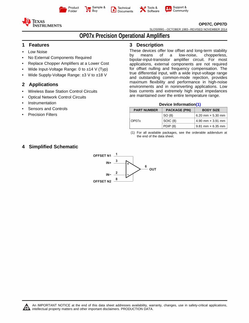
OUT - + OFFSET N2 IN- IN+ OFFSET N1 1 3 2 8 6 Product Folder Sample & Buy Technical Documents Tools & Software Support & Community OP07C, OP07D SLOS099G – OCTOBER 1983 – REVISED NOVEMBER 2014 OP07x Precision Operational Amplifiers 1 Features 3 Description These devices offer low offset and long-term stability 1• Low Noise by means of a low-noise, chopperless, • No External Components Required bipolar-input-transistor amplifier circuit. For most • Replace Chopper Amplifiers at a Lower Cost applications, external components are not required for offset nulling and frequency compensation. The • Wide Input-Voltage Range: 0 to ±14 V (Typ) true differential input, with a wide input-voltage range • Wide Supply-Voltage Range: ±3 V to ±18 V and outstanding common-mode rejection, provides maximum flexibility and performance in high-noise 2 Applications environments and in noninverting applications. Low bias currents and extremely high input impedances • Wireless Base Station Control Circuits are maintained over the entire temperature range. • Optical Network Control Circuits • Instrumentation Device Information(1) • Sensors and Controls PART NUMBER PACKAGE (PIN) BODY SIZE • Precision Filters SO (8) 6.20 mm × 5.30 mm OP07x SOIC (8) 4.90 mm × 3.91 mm PDIP (8) 9.81 mm × 6.35 mm (1) For all available packages, see the orderable addendum at the end of the data sheet. 4 Simplified Schematic 1 An IMPORTANT NOTICE at the end of this data sheet addresses availability, warranty, changes, use in safety-critical applications, intellectual property matters and other important disclaimers. PRODUCTION DATA.
Transcript
OUT
−
+
OFFSET N2
IN−
IN+
OFFSET N11
3
2
8
6
Product
Folder
Sample &Buy
Technical
Documents
Tools &
Software
Support &Community
OP07C, OP07DSLOS099G –OCTOBER 1983–REVISED NOVEMBER 2014
OP07x Precision Operational Amplifiers1 Features 3 Description
These devices offer low offset and long-term stability1• Low Noise
by means of a low-noise, chopperless,• No External Components Required bipolar-input-transistor amplifier circuit. For most• Replace Chopper Amplifiers at a Lower Cost applications, external components are not required
for offset nulling and frequency compensation. The• Wide Input-Voltage Range: 0 to ±14 V (Typ)true differential input, with a wide input-voltage range• Wide Supply-Voltage Range: ±3 V to ±18 V and outstanding common-mode rejection, providesmaximum flexibility and performance in high-noise2 Applications environments and in noninverting applications. Lowbias currents and extremely high input impedances• Wireless Base Station Control Circuitsare maintained over the entire temperature range.• Optical Network Control Circuits
• Instrumentation Device Information(1)• Sensors and Controls PART NUMBER PACKAGE (PIN) BODY SIZE• Precision Filters SO (8) 6.20 mm × 5.30 mm
OP07x SOIC (8) 4.90 mm × 3.91 mmPDIP (8) 9.81 mm × 6.35 mm
(1) For all available packages, see the orderable addendum atthe end of the data sheet.
4 Simplified Schematic
1
An IMPORTANT NOTICE at the end of this data sheet addresses availability, warranty, changes, use in safety-critical applications,intellectual property matters and other important disclaimers. PRODUCTION DATA.
OP07C, OP07Dwww.ti.com SLOS099G –OCTOBER 1983–REVISED NOVEMBER 2014
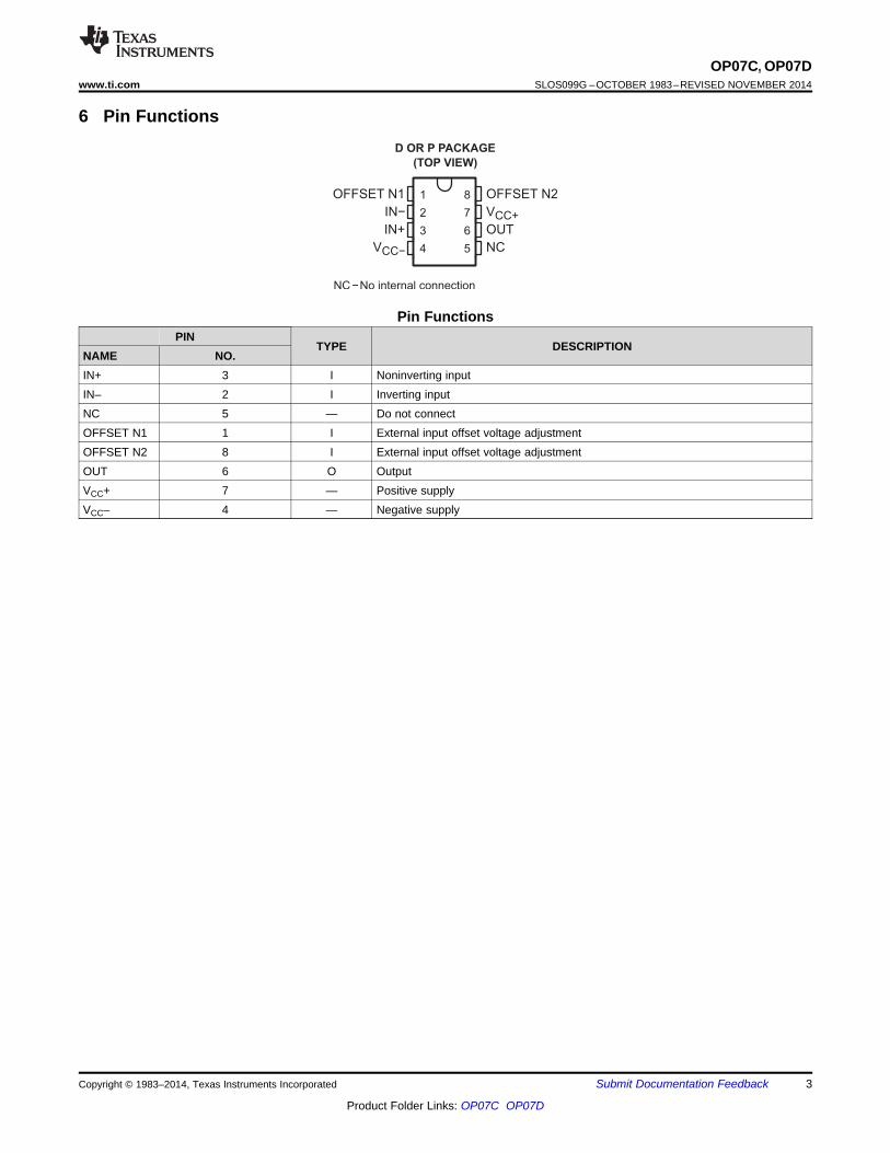
6 Pin Functions
Pin FunctionsPIN
TYPE DESCRIPTIONNAME NO.IN+ 3 I Noninverting inputIN– 2 I Inverting inputNC 5 — Do not connectOFFSET N1 1 I External input offset voltage adjustmentOFFSET N2 8 I External input offset voltage adjustmentOUT 6 O OutputVCC+ 7 — Positive supplyVCC– 4 — Negative supply
OP07C, OP07DSLOS099G –OCTOBER 1983–REVISED NOVEMBER 2014 www.ti.com
7 Specifications
7.1 Absolute Maximum Ratingsover operating free-air temperature range (unless otherwise noted) (1)
MIN MAX UNITVCC+
(2) 0 22Supply voltage V
VCC–(2) –22 0
Differential input voltage (3) ±30 VVI Input voltage range (either input) (4) ±22 V
Duration of output short circuit (5) UnlimitedTJ Operating virtual-junction temperature 150 °C
Lead temperature 1.6 mm (1/16 in) from case for 10 s 260 °C
(1) Stresses beyond those listed under Absolute Maximum Ratings may cause permanent damage to the device. These are stress ratingsonly, and functional operation of the device at these or any other conditions beyond those indicated under Recommended OperatingConditions is not implied. Exposure to absolute-maximum-rated conditions for extended periods may affect device reliability.
(2) All voltage values, unless otherwise noted, are with respect to the midpoint between VCC+ and VCC−.(3) Differential voltages are at IN+ with respect to IN−.(4) The magnitude of the input voltage must never exceed the magnitude of the supply voltage or 15 V, whichever is less.(5) The output may be shorted to ground or to either power supply.
7.2 Handling RatingsPARAMETER DEFINITION MIN MAX UNIT
TSTG Storage temperature range –65 150 °CHuman body model (HBM), per ANSI/ESDA/JEDEC JS-001, all 0 1000pins (1)ElectrostaticV(ESD) VDischarge Charged device model (CDM), per JEDEC specification JESD22- 0 1000C101, all pins (2)
(1) JEDEC document JEP155 states that 500-V HBM allows safe manufacturing with a standard ESD control process.(2) JEDEC document JEP157 states that 250-V CDM allows safe manufacturing with a standard ESD control process.
7.3 Recommended Operating Conditionsover operating free-air temperature range (unless otherwise noted)
MIN MAX UNITVCC+ 3 18
Supply voltageVCC– –3 –18 VVIC Common-mode input voltage VCC± = ±15 V –13 13TA Operating free-air temperature 0 70 °C
7.4 Thermal InformationTHERMAL METRIC (1) D P UNIT
25°C 7 32 7 32Supply-voltage sensitivitykSVS VCC+ = ±3 V to ±18 V, RS = 50 Ω µV/V(ΔVIO/ΔVCC) 0°C to 70°C 10 51 10 51
VO = 0, No load 80 150 80 150PD Power dissipation 25°C mW
VCC+ = ±3 V, VO = 0, No load 4 8 4 8
(1) Because long-term drift cannot be measured on the individual devices prior to shipment, this specification is not intended to be awarranty. It is an engineering estimate of the averaged trend line of drift versus time over extended periods after the first 30 days ofoperation.
(2) All characteristics are measured with zero common-mode input voltage, unless otherwise specified.
OP07C, OP07Dwww.ti.com SLOS099G –OCTOBER 1983–REVISED NOVEMBER 2014
9 Detailed Description
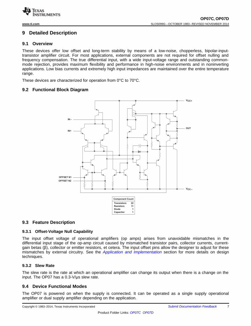
9.1 OverviewThese devices offer low offset and long-term stability by means of a low-noise, chopperless, bipolar-input-transistor amplifier circuit. For most applications, external components are not required for offset nulling andfrequency compensation. The true differential input, with a wide input-voltage range and outstanding common-mode rejection, provides maximum flexibility and performance in high-noise environments and in noninvertingapplications. Low bias currents and extremely high input impedances are maintained over the entire temperaturerange.
These devices are characterized for operation from 0°C to 70°C.
9.2 Functional Block Diagram
9.3 Feature Description
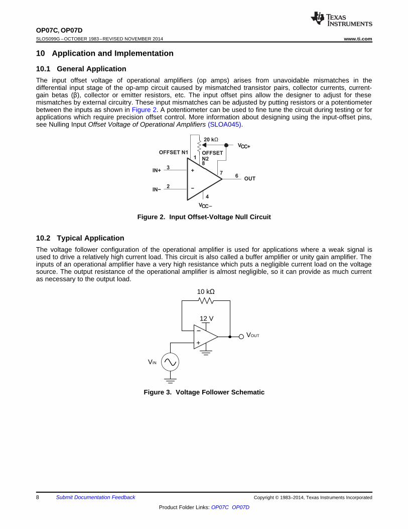
9.3.1 Offset-Voltage Null CapabilityThe input offset voltage of operational amplifiers (op amps) arises from unavoidable mismatches in thedifferential input stage of the op-amp circuit caused by mismatched transistor pairs, collector currents, current-gain betas (β), collector or emitter resistors, et cetera. The input offset pins allow the designer to adjust for thesemismatches by external circuitry. See the Application and Implementation section for more details on designtechniques.
9.3.2 Slew RateThe slew rate is the rate at which an operational amplifier can change its output when there is a change on theinput. The OP07 has a 0.3-V/μs slew rate.
9.4 Device Functional ModesThe OP07 is powered on when the supply is connected. It can be operated as a single supply operationalamplifier or dual supply amplifier depending on the application.
OP07C, OP07DSLOS099G –OCTOBER 1983–REVISED NOVEMBER 2014 www.ti.com
10 Application and Implementation
10.1 General ApplicationThe input offset voltage of operational amplifiers (op amps) arises from unavoidable mismatches in thedifferential input stage of the op-amp circuit caused by mismatched transistor pairs, collector currents, current-gain betas (β), collector or emitter resistors, etc. The input offset pins allow the designer to adjust for thesemismatches by external circuitry. These input mismatches can be adjusted by putting resistors or a potentiometerbetween the inputs as shown in Figure 2. A potentiometer can be used to fine tune the circuit during testing or forapplications which require precision offset control. More information about designing using the input-offset pins,see Nulling Input Offset Voltage of Operational Amplifiers (SLOA045).
Figure 2. Input Offset-Voltage Null Circuit
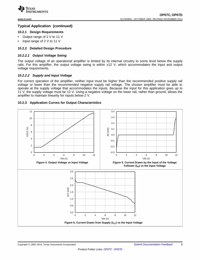
10.2 Typical ApplicationThe voltage follower configuration of the operational amplifier is used for applications where a weak signal isused to drive a relatively high current load. This circuit is also called a buffer amplifier or unity gain amplifier. Theinputs of an operational amplifier have a very high resistance which puts a negligible current load on the voltagesource. The output resistance of the operational amplifier is almost negligible, so it can provide as much currentas necessary to the output load.
OP07C, OP07Dwww.ti.com SLOS099G –OCTOBER 1983–REVISED NOVEMBER 2014
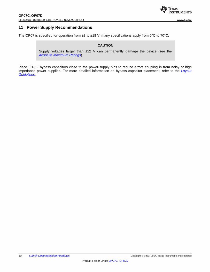
Typical Application (continued)10.2.1 Design Requirements• Output range of 2 V to 11 V• Input range of 2 V to 11 V
10.2.2 Detailed Design Procedure
10.2.2.1 Output Voltage SwingThe output voltage of an operational amplifier is limited by its internal circuitry to some level below the supplyrails. For this amplifier, the output voltage swing is within ±12 V, which accommodates the input and outputvoltage requirements.
10.2.2.2 Supply and Input VoltageFor correct operation of the amplifier, neither input must be higher than the recommended positive supply railvoltage or lower than the recommended negative supply rail voltage. The chosen amplifier must be able tooperate at the supply voltage that accommodates the inputs. Because the input for this application goes up to11 V, the supply voltage must be 12 V. Using a negative voltage on the lower rail, rather than ground, allows theamplifier to maintain linearity for inputs below 2 V.
10.2.3 Application Curves for Output Characteristics
Figure 4. Output Voltage vs Input Voltage Figure 5. Current Drawn by the Input of the VoltageFollower (IIO) vs the Input Voltage
Figure 6. Current Drawn from Supply (ICC) vs the Input Voltage
OP07C, OP07DSLOS099G –OCTOBER 1983–REVISED NOVEMBER 2014 www.ti.com
11 Power Supply Recommendations
The OP07 is specified for operation from ±3 to ±18 V; many specifications apply from 0°C to 70°C.
CAUTIONSupply voltages larger than ±22 V can permanently damage the device (see theAbsolute Maximum Ratings).
Place 0.1-μF bypass capacitors close to the power-supply pins to reduce errors coupling in from noisy or highimpedance power supplies. For more detailed information on bypass capacitor placement, refer to the LayoutGuidelines.
Run the input traces as far away from the supply lines
as possible
Only needed for dual-supply operation
Place components close to device and to each other to
reduce parasitic errors
Use low-ESR, ceramic bypass capacitor
(or GND for single supply) Ground (GND) plane on another layerVOUT
+RIN
RGRF
VOUTVIN
OP07C, OP07Dwww.ti.com SLOS099G –OCTOBER 1983–REVISED NOVEMBER 2014
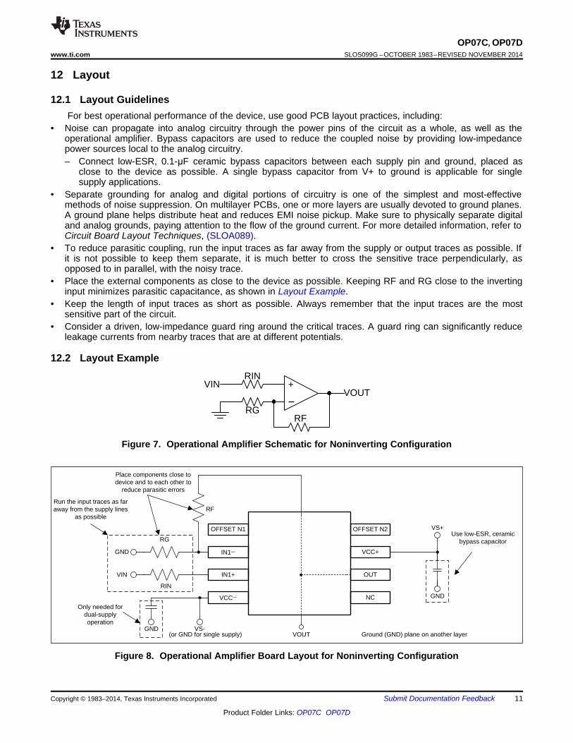
12 Layout
12.1 Layout GuidelinesFor best operational performance of the device, use good PCB layout practices, including:
• Noise can propagate into analog circuitry through the power pins of the circuit as a whole, as well as theoperational amplifier. Bypass capacitors are used to reduce the coupled noise by providing low-impedancepower sources local to the analog circuitry.– Connect low-ESR, 0.1-μF ceramic bypass capacitors between each supply pin and ground, placed as
close to the device as possible. A single bypass capacitor from V+ to ground is applicable for singlesupply applications.
• Separate grounding for analog and digital portions of circuitry is one of the simplest and most-effectivemethods of noise suppression. On multilayer PCBs, one or more layers are usually devoted to ground planes.A ground plane helps distribute heat and reduces EMI noise pickup. Make sure to physically separate digitaland analog grounds, paying attention to the flow of the ground current. For more detailed information, refer toCircuit Board Layout Techniques, (SLOA089).
• To reduce parasitic coupling, run the input traces as far away from the supply or output traces as possible. Ifit is not possible to keep them separate, it is much better to cross the sensitive trace perpendicularly, asopposed to in parallel, with the noisy trace.
• Place the external components as close to the device as possible. Keeping RF and RG close to the invertinginput minimizes parasitic capacitance, as shown in Layout Example.
• Keep the length of input traces as short as possible. Always remember that the input traces are the mostsensitive part of the circuit.
• Consider a driven, low-impedance guard ring around the critical traces. A guard ring can significantly reduceleakage currents from nearby traces that are at different potentials.
12.2 Layout Example
Figure 7. Operational Amplifier Schematic for Noninverting Configuration
Figure 8. Operational Amplifier Board Layout for Noninverting Configuration
OP07C, OP07DSLOS099G –OCTOBER 1983–REVISED NOVEMBER 2014 www.ti.com
13 Device and Documentation Support
13.1 Related LinksThe table below lists quick access links. Categories include technical documents, support and communityresources, tools and software, and quick access to sample or buy.
Table 1. Related LinksTechnical Support &Parts Product Folder Sample & Buy Tools & SoftwareDocuments Community
OP07C Click here Click here Click here Click here Click hereOP07D Click here Click here Click here Click here Click here
13.2 TrademarksAll trademarks are the property of their respective owners.
13.3 Electrostatic Discharge CautionThis integrated circuit can be damaged by ESD. Texas Instruments recommends that all integrated circuits be handled withappropriate precautions. Failure to observe proper handling and installation procedures can cause damage.
ESD damage can range from subtle performance degradation to complete device failure. Precision integrated circuits may be moresusceptible to damage because very small parametric changes could cause the device not to meet its published specifications.
13.4 GlossarySLYZ022 — TI Glossary.
This glossary lists and explains terms, acronyms and definitions.
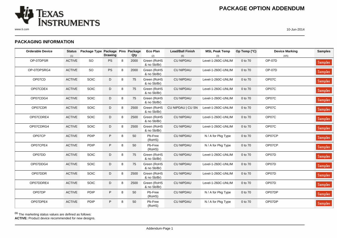
14 Mechanical, Packaging, and Orderable InformationThe following pages include mechanical packaging and orderable information. This information is the mostcurrent data available for the designated devices. This data is subject to change without notice and revision ofthis document. For browser based versions of this data sheet, refer to the left hand navigation.
LIFEBUY: TI has announced that the device will be discontinued, and a lifetime-buy period is in effect.NRND: Not recommended for new designs. Device is in production to support existing customers, but TI does not recommend using this part in a new design.PREVIEW: Device has been announced but is not in production. Samples may or may not be available.OBSOLETE: TI has discontinued the production of the device.
(2) Eco Plan - The planned eco-friendly classification: Pb-Free (RoHS), Pb-Free (RoHS Exempt), or Green (RoHS & no Sb/Br) - please check http://www.ti.com/productcontent for the latest availabilityinformation and additional product content details.TBD: The Pb-Free/Green conversion plan has not been defined.Pb-Free (RoHS): TI's terms "Lead-Free" or "Pb-Free" mean semiconductor products that are compatible with the current RoHS requirements for all 6 substances, including the requirement thatlead not exceed 0.1% by weight in homogeneous materials. Where designed to be soldered at high temperatures, TI Pb-Free products are suitable for use in specified lead-free processes.Pb-Free (RoHS Exempt): This component has a RoHS exemption for either 1) lead-based flip-chip solder bumps used between the die and package, or 2) lead-based die adhesive used betweenthe die and leadframe. The component is otherwise considered Pb-Free (RoHS compatible) as defined above.Green (RoHS & no Sb/Br): TI defines "Green" to mean Pb-Free (RoHS compatible), and free of Bromine (Br) and Antimony (Sb) based flame retardants (Br or Sb do not exceed 0.1% by weightin homogeneous material)
(3) MSL, Peak Temp. - The Moisture Sensitivity Level rating according to the JEDEC industry standard classifications, and peak solder temperature.
(4) There may be additional marking, which relates to the logo, the lot trace code information, or the environmental category on the device.
(5) Multiple Device Markings will be inside parentheses. Only one Device Marking contained in parentheses and separated by a "~" will appear on a device. If a line is indented then it is a continuationof the previous line and the two combined represent the entire Device Marking for that device.
(6) Lead/Ball Finish - Orderable Devices may have multiple material finish options. Finish options are separated by a vertical ruled line. Lead/Ball Finish values may wrap to two lines if the finishvalue exceeds the maximum column width.
Important Information and Disclaimer:The information provided on this page represents TI's knowledge and belief as of the date that it is provided. TI bases its knowledge and belief on informationprovided by third parties, and makes no representation or warranty as to the accuracy of such information. Efforts are underway to better integrate information from third parties. TI has taken andcontinues to take reasonable steps to provide representative and accurate information but may not have conducted destructive testing or chemical analysis on incoming materials and chemicals.TI and TI suppliers consider certain information to be proprietary, and thus CAS numbers and other limited information may not be available for release.
In no event shall TI's liability arising out of such information exceed the total purchase price of the TI part(s) at issue in this document sold by TI to Customer on an annual basis.
Texas Instruments Incorporated and its subsidiaries (TI) reserve the right to make corrections, enhancements, improvements and otherchanges to its semiconductor products and services per JESD46, latest issue, and to discontinue any product or service per JESD48, latestissue. Buyers should obtain the latest relevant information before placing orders and should verify that such information is current andcomplete. All semiconductor products (also referred to herein as “components”) are sold subject to TI’s terms and conditions of salesupplied at the time of order acknowledgment.TI warrants performance of its components to the specifications applicable at the time of sale, in accordance with the warranty in TI’s termsand conditions of sale of semiconductor products. Testing and other quality control techniques are used to the extent TI deems necessaryto support this warranty. Except where mandated by applicable law, testing of all parameters of each component is not necessarilyperformed.TI assumes no liability for applications assistance or the design of Buyers’ products. Buyers are responsible for their products andapplications using TI components. To minimize the risks associated with Buyers’ products and applications, Buyers should provideadequate design and operating safeguards.TI does not warrant or represent that any license, either express or implied, is granted under any patent right, copyright, mask work right, orother intellectual property right relating to any combination, machine, or process in which TI components or services are used. Informationpublished by TI regarding third-party products or services does not constitute a license to use such products or services or a warranty orendorsement thereof. Use of such information may require a license from a third party under the patents or other intellectual property of thethird party, or a license from TI under the patents or other intellectual property of TI.Reproduction of significant portions of TI information in TI data books or data sheets is permissible only if reproduction is without alterationand is accompanied by all associated warranties, conditions, limitations, and notices. TI is not responsible or liable for such altereddocumentation. Information of third parties may be subject to additional restrictions.Resale of TI components or services with statements different from or beyond the parameters stated by TI for that component or servicevoids all express and any implied warranties for the associated TI component or service and is an unfair and deceptive business practice.TI is not responsible or liable for any such statements.Buyer acknowledges and agrees that it is solely responsible for compliance with all legal, regulatory and safety-related requirementsconcerning its products, and any use of TI components in its applications, notwithstanding any applications-related information or supportthat may be provided by TI. Buyer represents and agrees that it has all the necessary expertise to create and implement safeguards whichanticipate dangerous consequences of failures, monitor failures and their consequences, lessen the likelihood of failures that might causeharm and take appropriate remedial actions. Buyer will fully indemnify TI and its representatives against any damages arising out of the useof any TI components in safety-critical applications.In some cases, TI components may be promoted specifically to facilitate safety-related applications. With such components, TI’s goal is tohelp enable customers to design and create their own end-product solutions that meet applicable functional safety standards andrequirements. Nonetheless, such components are subject to these terms.No TI components are authorized for use in FDA Class III (or similar life-critical medical equipment) unless authorized officers of the partieshave executed a special agreement specifically governing such use.Only those TI components which TI has specifically designated as military grade or “enhanced plastic” are designed and intended for use inmilitary/aerospace applications or environments. Buyer acknowledges and agrees that any military or aerospace use of TI componentswhich have not been so designated is solely at the Buyer's risk, and that Buyer is solely responsible for compliance with all legal andregulatory requirements in connection with such use.TI has specifically designated certain components as meeting ISO/TS16949 requirements, mainly for automotive use. In any case of use ofnon-designated products, TI will not be responsible for any failure to meet ISO/TS16949.
Products ApplicationsAudio www.ti.com/audio Automotive and Transportation www.ti.com/automotiveAmplifiers amplifier.ti.com Communications and Telecom www.ti.com/communicationsData Converters dataconverter.ti.com Computers and Peripherals www.ti.com/computersDLP® Products www.dlp.com Consumer Electronics www.ti.com/consumer-appsDSP dsp.ti.com Energy and Lighting www.ti.com/energyClocks and Timers www.ti.com/clocks Industrial www.ti.com/industrialInterface interface.ti.com Medical www.ti.com/medicalLogic logic.ti.com Security www.ti.com/securityPower Mgmt power.ti.com Space, Avionics and Defense www.ti.com/space-avionics-defenseMicrocontrollers microcontroller.ti.com Video and Imaging www.ti.com/videoRFID www.ti-rfid.comOMAP Applications Processors www.ti.com/omap TI E2E Community e2e.ti.comWireless Connectivity www.ti.com/wirelessconnectivity