General Note TT Electronics reserves the right to make changes in product specification without notice or liability. All information is subject to TT Electronics’ own data and is considered accurate at time of going to print.
Description The OPB9000 is a versatile sensor that can be used in a wide variety of industrial and medical applications. The sensor features market-leading ambient light immunity which allows operation from dark rooms to bright sunlight. It can detect various types of media with as little as a 30% change in reflectivity. Robust, industrial grade resin allows the sensor to operate at a wide temperature range from -40C to + 85C, ideal for the harshest environments. Factory calibrated to a white card at a 12mm distance to offer plug and play detection, the OPB9000 can be re-calibrated in a matter of milliseconds with a single command for specific application requirements. Integrated automatic temperature compensation maximizes detection consistency and reliability. The small footprint saves valuable PCB real estate as devices become smaller and more portable. The OPB9000 eliminates the need for peripheral circuitry like op-amps, data converters, and comparators, as all analog signal conditioning is integrated in the IC. Applications
All non-contact position sensing and presence detecting applications Industrial printing and high-speed paper detection Manufacturing and automation Automated banking machines Hospital and lab equipment Portable medical equipment Automatic dispensing Material handling and asset tracking
Features Market leading 25k+ lux ambient light immunity Programmable output configuration and sensitivity level Single-command calibration with on-chip EEPROM Temperature-compensated LED drive 6µs response time Pulsed synchronous drive-detection Surface mount package
General Note TT Electronics reserves the right to make changes in product specification without notice or liability. All information is subject to TT Electronics’ own data and is considered accurate at time of going to print.
General Note TT Electronics reserves the right to make changes in product specification without notice or liability. All information is subject to TT Electronics’ own data and is considered accurate at time of going to print.
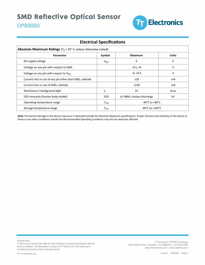
Note: Permanent damage to the device may occur if operated outside the Absolute Maximum specifications. Proper function and reliability of the device at these or any other conditions outside the Recommended Operating Conditions may also be adversely affected
General Note TT Electronics reserves the right to make changes in product specification without notice or liability. All information is subject to TT Electronics’ own data and is considered accurate at time of going to print.
General Note TT Electronics reserves the right to make changes in product specification without notice or liability. All information is subject to TT Electronics’ own data and is considered accurate at time of going to print.
General Note TT Electronics reserves the right to make changes in product specification without notice or liability. All information is subject to TT Electronics’ own data and is considered accurate at time of going to print.
General Note TT Electronics reserves the right to make changes in product specification without notice or liability. All information is subject to TT Electronics’ own data and is considered accurate at time of going to print.
Test Notes 1. Excludes LED pulsed drive current. 2. Time at power-up between VDD settling to within 0.1V of its steady-state level and CAL going high at the end
of the SETTLE mode interval. 3. Time from start of pulse to the point at which the pulsed current reaches within ±1% of the final level and
remains in that range for the remainder of the pulse. 4. Time from OUT going low at the midpoint of the first bit (‘b0) to OUT going high at the midpoint of the
second bit (‘b1); should be equal to 10*tPER(T). 5. Time from CAL going high (indicating completion of internal read command) to OUT going low (start of
Manchester-encoded LSB of data being read). 6. Equal to 2 to 3 LED pulse periods. 7. CAL going low and high (for ‘b0 or ‘b1 input bit, respectively) at the time from midpoint of one input bit to
CAL going low or high at the midpoint of the next input bit; should be equal to 10*tPER(T). 8. Time from CAL going low or high (for ‘b0 or ‘b1 input bit, respectively) at the midpoint of one input bit to CAL
going high or low at the beginning of the next input bit; only applicable if the next input bit is of opposite polarity.
9. Time from CAL going high at the midpoint of the last input bit of the calibration command sequence to CAL going low at the end of a successful calibration; absence of CAL going low within this interval means that the calibration failed.
10. Time from CAL going low at the end of a successful calibration to the subsequent CAL going high. 11. Applicable for read command sequences and for write sequences if the last data input bit is ‘b1: time from
CAL going high at the midpoint of the bit (last data input bit for writes, last command-code bit for reads) to the CAL going low following the end of the last data input bit.
12. Time from CAL going low either after the end of the last data input bit of the write command sequence (if that bit is ‘b1) or at the midpoint of that bit (if that bit is ‘b0) to the subsequent CAL going high. Includes any stabilization time required for newly programmed [REF] setting.
13. Time from CAL going low after the end of the last command-code bit of the read command sequence to the subsequent CAL going high.
14. “Immune” = “optical input threshold moves by ≤5%” 15. [(LED resulting from calibration @ T) / (LED resulting from calibration @ 40°C)] - 1. 16. LSL 0.02*VDD for f ≤ 10 kHz, 0.01*VDD for f ≤ 50 kHz, 0.005*VDD for f ≤ 1 mHz.
General Note TT Electronics reserves the right to make changes in product specification without notice or liability. All information is subject to TT Electronics’ own data and is considered accurate at time of going to print.
General Note TT Electronics reserves the right to make changes in product specification without notice or liability. All information is subject to TT Electronics’ own data and is considered accurate at time of going to print.
General Note TT Electronics reserves the right to make changes in product specification without notice or liability. All information is subject to TT Electronics’ own data and is considered accurate at time of going to print.
General Note TT Electronics reserves the right to make changes in product specification without notice or liability. All information is subject to TT Electronics’ own data and is considered accurate at time of going to print.
General Note TT Electronics reserves the right to make changes in product specification without notice or liability. All information is subject to TT Electronics’ own data and is considered accurate at time of going to print.
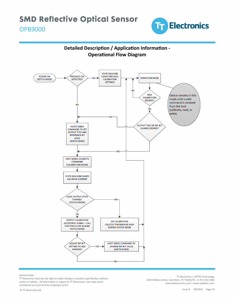
The OPB9000 is a reflective CMOS sensor with calibration features and programmable sensitivity and output type. The monolithic CMOS receiver/LED driver controls all functional modules of the device, including calibrate/status, read/write, and operate. The device can be calibrated to detect various reflective surfaces at different distances. An on-chip EEPROM is used to store the calibrated LED drive current level, sensitivity level, and output type, allowing the sensor to return to the correct levels and states upon the next power-up cycle. A brief status mode follows every calibration sequence allowing the user to ensure that the calibration was successful. The LED drive current remains in operation mode until a valid command is received (calibrate, read, or write). Output types and threshold levels can be programmed as part of the calibration process. The default output type is inverter (signal detected, output low), totem pole (push-pull). The output can be programmed to detect either a decreasing signal level or an increasing signal level, but not both at the same time. The filtered amplifier output is integrated for comparison to a 4 bit programmable threshold voltage and the result determines the device output state. If the amplifier output is above or below the threshold voltage for 2 consecutive LED pulses, the output will switch to the proper state. The actual logic level is dependent upon the output type that has been programmed (table 1). The OPB9000 includes an on-chip photodiode which feeds a bandpass filtered analog front end amplifier to accomplish ambient light immunity as well as signal amplification. An LED driver pulses the LED for 250ns at a pulse rate of 2us (12.5% duty cycle). The OPB9000 switches states when the reflected signal decreases by approximately 50% from the calibrated level. The device includes temperature compensation over its operating temperature range as well as plastic lensing over both LED and detector to narrow the beam spread/viewing angle and maximize detection distance capability.
General Note TT Electronics reserves the right to make changes in product specification without notice or liability. All information is subject to TT Electronics’ own data and is considered accurate at time of going to print.
Calibration The OPB9000 may be programmed to a specific output type and sensitivity level, then self-calibrated against a specific target at a specific distance from the sensor face. By default, the output is inverted in a push-pull configuration (i.e. output is low when object is detected). The sensitivity level is set for detection of a 90% diffuse reflectance white card at a distance of 12mm, and a change of state when the reflected signal drops by approximately 50%. This default setting is sufficient for use in many applications. The user can re-program and re-calibrate the device for a specific application. During a calibration process, the pulsed LED drive is ramped from 3 mA to approximately 85 mA (at the above mentioned pulse duration and pulse period) until the reference level is reached for two consecutive pulses. The LED drive current value is then stored in an EEPROM bank. The ramping period is 17mS max; a subsequent STATUS mode is active for an additional 13 mS. After a calibration request is sent, and during the ramping period, the CAL/STAT pin will be in a high state. After the ramping period ends with a successful calibration, the pin will transition to a low state for the STATUS mode (as seen in the screenshot). If the calibration is unsuccessful, then the CAL/STAT pin will remain high for the STATUS mode period. An unsuccessful calibration can occur if no reflective surface is present or insufficient light is received during the process.
General Note TT Electronics reserves the right to make changes in product specification without notice or liability. All information is subject to TT Electronics’ own data and is considered accurate at time of going to print.
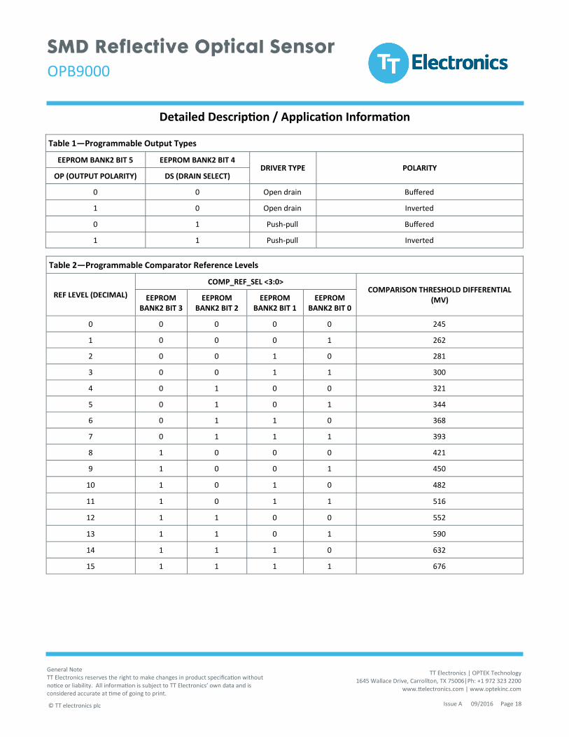
Programmable Sensitivity Levels The sensitivity level is determined by the difference in the reference level settings between Command 1 and Command 3 in the previous section. See table 2 for available reference level settings. Below are a few examples of sensitivity level settings.
Example 1: A device is programmed to a reference level setting of 2 during the writing of command 1 to the device. This establishes a relatively low trip threshold of approximately 281 mV during the LED calibration step (Command 2), which would normally be needed in cases where the reflected light levels are low, e.g. the target surface has low reflectance and/or the target is far from the device. In cases where the target is more reflective or closer to the sensor, a higher reference level could be selected if desired. In general, the higher the reference level used for the Command 1 write, the higher the LED drive required to calibrate the device. During the writing of Command 3 to the device, the reference level setting is changed from 2 to 0. This establishes the comparator trip level at approximately 245 mV. This level is 87% (245/281) of the level used to calibrate the LED drive. Therefore, an approximate 13% reduction in light level will now cause the output state to change.
Example 2: A device is again programmed to a reference level setting of 2 during the writing of command 1 to the device. During the writing of Command 3 to the device, the reference level setting is changed to 6, causing an immediate output state change to its pre-calibrated level. Ref level 6 establishes the comparator trip level at approximately 368 mV. This level is 131% (368/281) of the level used to calibrate the LED drive. Therefore, an approximate 31% increase in light level will be required to cause the output state to change.
Example 3: A device is programmed to a reference level setting of 14 during the writing of Command 1 to the device. During the writing of Command 3 to the device, the reference level setting is changed to 3. This level is 47% (300/632) of the level used to calibrate the LED drive. Therefore, an approximate 53% decrease in light level will be required to cause the output state to change.
The procedure for calibrating the OPB9000 usually includes sending three commands to the device on the calibrate/status pin. Those commands are as follows:
Command 1 — send write command to set output type (OP and DS bits, table 1) and comparator reference level bits (table 2)
Command 2 — send command to calibrate LED drive
Command 3 — send write command to change comparator to new desired reference level (to adjust detection sensitivity)
EEPROM STRUCTURE
BANK 1 (13 bits) (READ ONLY)
LED drive counts (10 bits) NOT USED (2 bits) Calibration successful (1 bit)
General Note TT Electronics reserves the right to make changes in product specification without notice or liability. All information is subject to TT Electronics’ own data and is considered accurate at time of going to print.
Communication Standard The Manchester Code follows the standard IEEE 802.3:
“0” is expressed as a midpoint high-to-low transition, “1” is low-to-high transition
Encoded output = data XOR clock The waveform chart below shows the Manchester encoded output for each possible two bit sequence. Commands
All commands sent to the OPB9000 are sent via the CAL/STAT pin. Each command must first begin with the syncing nibble (1100). The first two bits “11” allow the decoder to detect the data clock. The second two bits are a check for detection of the “00” data. The third two bits determine the command being sent. The available commands are:
1100-00 Reserved (do nothing)
1100-01 Read request
1100-10-bbbbbb Write Bank 2 bits
1100-11 Calibrate request For a read or calibration request, there will be 6 bits: “1100-01” or “1100-11” respectively:
General Note TT Electronics reserves the right to make changes in product specification without notice or liability. All information is subject to TT Electronics’ own data and is considered accurate at time of going to print.
Commands (cont.) For a Write Bank 2 command, there will be a total of 12 bits: “1100-10-bbbbbb”, where the last 6 bits are data to be written to EEPROM. These 6 data bits are defined in table 1 (OP,DS bits) and table 2 (comparator REF bits 0-3). The sequence of transmission of these bank 2 bits must be from most significant to least significant bit—ie. bit 5 to bit 0 (after syncing nibble and two clock detection bits). The data rate for the write command is 100 kb/s [+100 kb/s, -50 kb/s]. Read Request Data Bit Sequence and Rate The read request will serially transmit Manchester-encoded data (100 kb/s at 50% duty cycle, ±5 kb/s), from the Vout pin, the EEPROM bank values and also include an error flag. A total of 37 bits will be transmitted including a zero as the first bit and an error flag bit as the 2nd bit. Example is shown in below figure.
General Note TT Electronics reserves the right to make changes in product specification without notice or liability. All information is subject to TT Electronics’ own data and is considered accurate at time of going to print.
Commands (cont.) Error Flag After data is written to a bank of EEPROM, the state machine will compare the content (read out from the same bank) to the data written in. Normally the read data is the same as the write data, but if there is a difference, the Error Flag will be set to “1”. Communication Pins The CAL/STATUS pin is used to write data to the OPB9000 and the initiate a calibration sequence. This pin is also used during the STATUS mode to output the status of an attempted calibration. See Calibration section of this data sheet for more information. The Output pin is used to read the value of all EEPROM bits. See previous section (Commands) for more information.
General Note TT Electronics reserves the right to make changes in product specification without notice or liability. All information is subject to TT Electronics’ own data and is considered accurate at time of going to print.
General Note TT Electronics reserves the right to make changes in product specification without notice or liability. All information is subject to TT Electronics’ own data and is considered accurate at time of going to print.
General Note TT Electronics reserves the right to make changes in product specification without notice or liability. All information is subject to TT Electronics’ own data and is considered accurate at time of going to print.