SOLID STATE VARIABLE FILT ER MODEL 3550 SERIAL NO. __ OPER AT I G AND AINT NANCE MA NUAL KRD - ITE CD R PCRAT ID Avon Industrial Park/Bodwell St., Avon, Massachusetts 02322 CD 1975 KROHN - HITE CORPORATION
Transcript
SOLID STATE
VARIABLE FILTE R
MODEL 3550 SERIAL NO.__
OPERATI G AND AINT NANCE
MANUAL
KRD - ITE CDR PCRATI D Avon Industrial Park / Bodwell St., Avon, Massachusetts 02322
CD 19 75 KROHN- HITE CORPORATION
C o n t e n ts
CO NTENTS Se c ti on
1 GENERAL D ESCRIPTIO N . . . . . . . . . 2 O P E R A T ING I STRUCTIONS . . • . . .. 3 IN COMING A C CEPTANCE AND INSPECT IO N 4 CIRCUIT DESCRIPTIO N . . . • . 5 MAINTEN A NC E ....•.. 6 C A L IB R A T IO N A N D ADJ US T M E N T
ILLUSTRATIONS
F igure
1-1 M o d e l 3 5 50 M u lt ifu n c t i o n F i l te r . 2-1 F r o n t and Rea r Pa ne ls . 2-2 Pas s Ban d C ha r a c t e r i s t i c s . 2 - 3 Normalized Attenuati o n C h a r a te r i s t i c s 2 - 4 S q u a re Wa v e Response ..' . .... 2- 5 P ha s e Shift . . . . • •e •
4 -] loc k Diagram . . • • . . . . . ' 4 - 2 R e s p o ns e of Q u a d r a t i c A mplifie r s • 5 - 1 Trims and A d j u stm e nt s . .. Appendix
S c h e m a ti • Layout a nd P a r ts L i s t
TABLES Table
3 - ] Ac c e p t a n c e C h e c k o u t P r oc e d u r 5- ] Te s t P o i n t v s S ig n a l Volta g e 6 - 1 Cal ib r atio n P ro c e d u r e . . . .
P a g e
I 4
I I
15 20 24
P a g e
ii 5 8 8 8 9
16 17 21
~ E nd
Pag e
12 22 26
F ilt er, 3 550
. 1 . 10 ,100 .IK
INPUT I<ROH -HITE
mode . 3550 filter
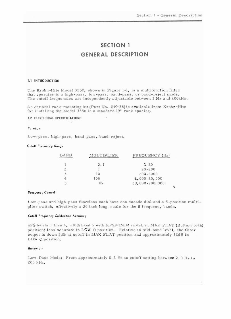
F ig u r e 1-1, Model 3550 Multifunction Filter
ii
Section I - General Descripti on
SECTIO N 1
GENERAL DESCRIPTION
1.1 INTRODUCTION
T h e K r oh n - H i t e Mo de l 3550, shown i n F igure 1-1, is a multifunc tion filte r that op e r a t e s in a h igh -pa ss , low -pass , band-pass , or band -reject mode . The c ut o ff frequencie s a r e independently a dj u s t a b l e between 2 H z and 2 00kHz .
A n optional rack -mounting kit (P a r t No . RK - 3 8) is a vailable f r om Kr oh n -Hi t e (or install ing th e Model 3550 in a standard 19" r a c k spacing .
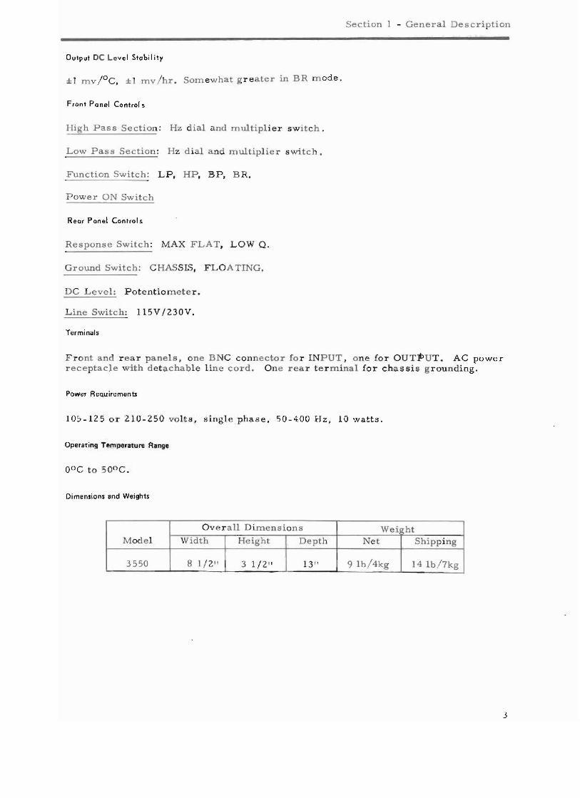
1.2 ELECT RICA L SPECI FICAT IONS
Function
L o w -pas s , h i g h - p a s s , b a n d - p a s s , band- reject.
Cutoff F requenc y Range
BAND M UL T IP L I E R F REQUENC Y ( Hz )
I O. 1 2 - 20 2 I 20 - 200 3 10 20 0 -200 0 4
5 l Oa
lK 2, 000 -20, 000
20 , 000 - 200, 000 \
F requenc y Can1 ,01
L o w - p a s s and high-pass functions each have one decade dial and a 5 - position multi plie r s witch, e ffe c t i v e l y a 3 0 inch l o n g scale fo r the 5 fr eq ue n cy band s .
Cutoff Frequency Cal i brc tion Accu 'a cy
±50/0 bands 1 t h r u 4 , ±lO% band 5 w i t h RESPONS E s witch in MA X F LAT (B u t t e r w o r t h ) pos i tion ; l e s s a c c u r a t e in L O W 0 p ositio n . Rela tiv e t o m id- b a n d l e v e l , the f il t er o u t pu t i s d o w n 3d B a t c u t off i n MAX F LAT position a nd app roximate l y .12.d B i n L O W 0 p o s i tion.
Bandwidth
Low -Pass Mode : F rom a pproximate ly 0 .2 Hz to c u to ff setting betw e e n 2. °H z to 200 k Hz ,
Filter, 3550
Hig h -Pass Mod e : F r o m c u to ff s e tt ing o f 2. 0 Hz to 2 00 k Hz , t o app rox imat e l y 3 M Hz.
Band-Pass: Both cutoffs a djustabl e from 2 . 0 Hz t o 2 00 k Hz , F o r m i n im um ban d w i d t h (Butte rworth response ) both c u t off fr equencies a r e s e t to c o i n c id e . Th i s p r oduce s a n inse rt ion loss of 6 dB, w i t h the 3dB p o ints a t 0 .8 and] . 2 5 time s the mid-band freque nc y .
Band-Reject: B ot h cutoff f r e que ncies a d j u s t a ble f r om 2. 0 Hz t o 20 0 k Hz . Lower pass b a nd t o app r oximately 0. 2 Hz , upper passband to app r o ximatel y 3 MHz . A sha rp null can be ob ta in e d b y s etting the Hig h Pass s e c t i o n to about twice t h e null fr eque n c y, a nd t he L o w P a s s s e cti on t o half t h e null f r e qu e n cy, a n d a l t e r n a t e l y a djusting both d ial s f o r minim um r e s p on s e .
Response Charocteristi c s
Choice of 4 p ol e Butte rwo r th (Maximally fi a t res p on s e ) f o r fr e q u e n c y d om a in op e r a tion and L ow Q (dam p e d res p on se) for tr a n s ient - fr e e tim e d o m ain operation, selected by mean!') of a switch on the rear p a n e l.
Attenuation Slope
Nominal 24 dB per o ctav e In all rn od e s of o pe r a ti on .
Pa$S Band Gain
Zero db + 1 db in pass band.
Maxi mum Attenuat ian
Greater than 60 dB
Input Character; stic 5
Max Voltag e : ±7V peak to 2 MHz.
Max DC Component: ±lOOV.
Input Irnpedance : 10 Megohms in parallel wit h 50 pi.
Output Characteri 51iC5
Max Voltage : ±7V peak to 2 MHz.
Max Current: ± 15 rna peak.
Internal Imped a n c e : 50 ohms.
Hum lind Hoi se
Less than 200 uv , except 400 uv in "BAND REJECT" rn od e ,
2
Section 1 - General De sc ript ion
Output DC Leve l Stobi I ity
± l m y / oC t ± l rnv Zh r . Som e what g r e ater in BR m od e .
Front Panel Control s
High Pass Section : Hz d i a l a n d m ultipl i e r swi t c h.
Low Pass Section : Hz d ial a n d multiplie r s witc h .
Function Switch : LP, HP, BP, E R .
P o w e r ON Switch
Reor Ponel Control s
R e s p ons e Switch : M AX FLAT, LOW Q.
G r o und Switch : C HAS S IS, FLOA TING .
DC L e v e l : P otentio m e t er.
L i n e Swit ch: 115V /230V.
Terminals
F ron t and r e ar p a nel s , o n e E N C con n e c t o r f o r IN P UT, o n e for OU TPUT. AC power r e c e p t a cl e w i t h d e t achab l e l in e cord . On e r e a r termina l for cha ssi s g r ou n d i ng .
POWIIT Henuirernants
105-125 or 210-250 volts, single phase, 50-400 Hz, 10 watts.
Operating Temperature Range
occ to 5 0a C .
Dimensions and Weights
M odel
Overa ll D im e n s i o n s We i ht W id t h Height Depth Ne t Shipp ing
3550 8 1/ 2" 3 1/ 2 " 13 " 9 Ib/4kg 14 Ib / 7k g
3
F ilt e r , 3 5 50
SECTION 2
OPE RATI NG INSI CIIONS
2.1 INITIAL SETUP
T he fi lte r is a d jus ted and checked c a r efull y in our test department to insure t ha t it mee t s all specifications . It i s then a g e d and tested again befo re shipment . The filter is shipped complete and a f t e r unpacking is read y for use.
The M od e l 3550 s h o uld be unpacked c a r e f ull y and in s pe cted for damag e that ma y h ave o c c u rr e d in s hipping . Check all controls for freedom of ope ration .
T he Filte r may be o p e r ate d from an A C p ow e r s ource o f e ithe r 10 5- 12 5 v o lt s , 50 - 4 0 0 H z , or 2 10 - 2 5 0 vo lt s , 50 - 4 0 0 H z . A I1 5 / 2 30 V LINE wit c h , l oc a t ed o n the r ear p a nel , s e l e c t s t he filt er' s mode o f ope r at ion , W hen t he AC line i s 11 5 V, m o ve t he LIN E s w i t c h to t h e I 15V po sitio n . In t hi s mod e , a 1 / 8 ampe r e 5 10- b lo fu s e ITlUS t b e u s e d . W h e n t h e fi lte r i s t o be o p e r a ted f rom 2 3 0 VAC , m ove t he L I NE s witch to t he 2 30V po sit io n, and r e pla c e t he fu s e w ith a 1 / 16 amp e r e slo -blo t y p e .
2.2 CONTROLS AND TERMINALS (figure 2-2)
2.2.1 Fro" I Ponel
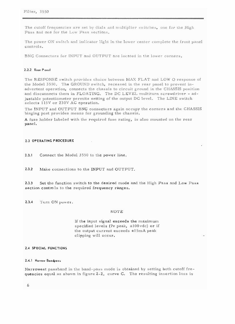
T he fun c tion s witch in the top center of the front panel selects on e of fou r fi ltering f unctions : L ow P a s s (L P ), Hig h P a s s (H P ), Band P as s (B P), o r B a nd R e j e c t (B R ) .
The cutoff frequencies are s e t by d ial s and rn ul t i pl i e r s w it c he s , o n e fUI' the Hig h P a s s a nd one fo r t h e LLl\\ Pass s e c ion s.
T he p owe r O N sw i tch and indicato r lig ht in the l owe r cen ter complete th e f r on t panel c on t r o l s .
B N C C onn ec tors fo r INPUT a n d OUTPUT a re loc at ed i n I he l ow e r co rners .
2.2.2 Rear Panel
The R E S P O SE s w i tc h provides c h o ice b e tween M AX FL AT and LO\.\,' 0 r e spo n s e of t he Model 3 5 50 . T he G R O U. ' D swit c h, r e c e s s e d in t h e r e ar panel t o p r e v en t i n adver tent operati on, c o n n ec ts th e chass is to ci rcuit g round in t ne CHASSIS p o s i t ion and disc onne cts them in F LOATI G . T he DC L E V EL mul ti tu r n s c r e w d riv e r - ad j u stabl e potentiometer p ermits se tting of the ou t pu t D C l evel. T he LINE s w itc h s elect s 115 V r 2 3 0 V A C o p e ra t i o n .
The IN P U T a n d O UT P U T B NC c o nn e c to r s a gain oc cupy t he c o r n e r s a nd t h e CHASSIS binging po s t p rovides m eans for grounding the chassis .
A fuse holder l a b e l e d w i t h the r e qu i r e d fus e rating , i s a lso mounted on the l' a r pane l.
2.3 OPERATING PROCEDURE
2.3.1 Conn ect t h e M od el 35 50 to the power line.
2.3.2 M a ke c o nn e ct i on s t o the INP UT and O UT P U T.
2.3.3 Set t h e f u n c t i on s w i tch to the d e s i r e d m od e a nd the High P a s s a n d Low Pa s s section cont ro l s t o t h e r e q u i r e d f r e q u e n c y range s.
2.3.4 T u r n ON pu\'.,'er.
NOTE
If th e i n pu t s ig n a l exceeds the m a x im u m spe c i fied lev el s (7v p e a k , ± I OOvdc ) or if the o ut pu t c u r r e n t e x c e e d s ± 15m A p e a cl i pp i ng w ill oc c u r .
2.4 SPECI AL FUNCTIONS
2.4.1 Narrow Bon dposs
Nar r owe s t pass band in the b a nd - p a s s mod e i s obta ined b y s e tt i n g b o t h c ut o ff frequencie s eq u a l a s s how n in figu r e 2-2, c u r v e C. T he r e s ul t in g i n s e r t i on los s is
6
Section 2 - O p e r a t i n g Instructions
6 d B, (at band c e n te r) , and the 3 dB points ar e at a b out 0 .8 and 1. 25 times m id b a n d frequency .
2.4.2 Null
A s h a r p null can be obtained in t h e Band Rej e c t m od e by setting the L o w Pass section t o half the n ull f r e quen c y a n d the High Pas s section t o t wic e t h e n ull frequency and a lte r nately adj us t ing b o th d i al s to m in i m i ze the ou tpu t. Fig u r e 2 - 2, Curve D.
2.4.3 Maxi mom Flot vs , Low Q Respon ses
In the MAX FLAT p o s it i on of this rear - pa n e l switch the fil t e r resp o n s e i s a fo u rth o r d e t: B u t t e rwor t h function:
VI + S8
VI + S8
G = gain
f S --
fa
f = f r e q ue n c y
f a = c u t off fr e quency setting
This r s p o ns e is p l o t t e d as the s o li d cu r ves i n F igur 2-2, curv e s A a n d B , a.nd normalize d o n ~ large r s c a l e as i n F i g u r e 2-3. It h ug s the O- d B l i ne very close l y w i.t h n o r i ppl s a Irn os t t o t h e cuto ff frequ ency , a nd t he n k.ee p s clo s e t o the 24d B /octa v e a s sym p to te , depa r t i ng IdB fr om these l irie s at f /fo= 0. 8 and 1. 2 5 r e spect ively.
The lim ita tion s of thi s t y pe of filt e r a r e apparen t i n F ig u r e 2-4(al which shows the s t e p- func t ion r e s ponse of a fo u rth o r d er Bu t te r w or t h l ow pas s . Fo r a p pli c at i ons where t h i s eleven per c ent ov e r s h o o t canno t b e t ol e rated, the Mod el 3 55 0 p r ov id e s the L O W 0 p o s i tion of the R ES PONS E s witch. In this m od e t h e sha rpness of t h e r.u t o ff i s r e d u c ed jus t enough t o elimi n a te t h e s t e p - func tion ove r shoo t ( s e e Fig u r e 2-4(b)}. T h e f r e que n c y r e s p on s e of t he L O W Q mod e is s hown b y the d ott ed c urv es in Fig u r e 2 - 2 (cu r-v e s A a n d B). Obviously, t h e cutoff i smu c h Le s s sha r p , t h e a tte n u a tion at the c o r n e r i s a pproximately 12 dB and the I dB p o in t s ar e a t 0.2 a nd 5 tim e s the cutoff frequ e ncy.
T h i s reduction o f cutoff sharpnes s h a s n o r e al m eani ng fo r a high - pa s s filter b u t w a s i n cluded in t h e M od e l 3 550 h i g h p a s s sect ion to prov i d e sym metrical band p a s s and band reject curv e s w hen the LO W Q mode is u s e d .
7
F il t e r , 3 5 50
A - LOW PASS B - HIGH PASS
..... " <, 1\
1\\ ~~ \ \ \ I \
I \ I \ I I
dbdb
oo
-20-20
-40-40
-60 -60 20Hz 200KHz 2MHz
C-BAND PASS
100 IK 10K lOOK 1M Hz
I
.' /'" '-1
/ \ ~\
/ \ 1\ I I / \ I \
I ' I \ , \ I I I \ I
dbdb
oo
-20-20
-40-40
-60-60 .I 10 .1
: l i/ '" {./ III, ~ :
I I I I I I I I I
I I I I
20Hz 200KHz 2MHz
0- BAND REJECT
-, \ ( /
I' ~ V,
\ I \ I 1 \ I I
I I
10 100 IK 10K lOOK 1M Hz
Figure 2 -2. Pass Band Char a ct e r i s t i c s
o
2
- --.... 1\\
-, \\ '\ \ , \ \ \
\
\ ,\
I HPot< IGli PASS OJlOtT FREC'JENCY '.\ fLP'LOW PASS CUTOFF fREQUENCY \\
I II \
I II .\
(a)- 6
_ - 12
'" ':. ~ - 18
'" Il:
~ -24 -' i::
- 3 0
- 42 I 3 4 5 6 7 891 2 ~ 4 56 18 10
(b )-OR !liE f LP f
Fig ure 2- 3.
No r m a l i z e d A tte nua t i o n C h a r a c t e ris tic s F i g ur e 2-4. Squ a r e Wa ve R e s p o ns e
8
Sect ion 2 - O pera ting Instructions
2. 4.4 P hase Re spons e
T he pha s e s h ift i n each sec ti o n o f t h e fi lte r i s s ho w n in F igure 2 - 5. I n the dra wing a p o s i t ive angle m e a n s p hase lead , i. e . I t h e out put v olta g e lea d s inpu t v o ltage . T h e solid cu r ve is fo r MA X FLAT mode , and the d otted c u r ve f or LO W Q m ode .
Wh e n the M o d e l 3 5 50 i s used for bandp a s s , b o th sec tion s are casca de d (s e e Sec tio n 4 ) a nd p has e shi ft s a dd a lge b raically . N o te t hat at p a s s b a nd cente r f r eq u en c y (f = fHfL ) the pha s e s hift i s z e r o. A n examp l e of t h e compu tat i o n o f pha se s h i ft i n t h e b a nd pas s mode follo ws :
Giv en : P a s s band 10 0 Hz to 500 Hz (i . e . Hi h Pa ss s e c t i on se t t o 10 0 Hz a nd th e Low Pass section se t to 500 Hz . . )
F in d : P h a s e shift a t 200 H z MAX F LA T res pon s e
200 Hz1. High pass r e l a t i v e f r e qu e n cy = = 2 . 0
100 Hz 200 Hz
2. L ow P a ss r e l a t i v e freq uenc y = = 0 . 4 500 Hz
+ 360
t:::---......... --.... - r-, <,
f"'-.,. r-..<, .... ' ... f'\I'
, : \
~~
1\' \: ' ,
"""....,
<, ............ " ...... ...... .......I--
. .... ..... .~
-r-. I--
o
-60.30 0
lJ} lJ} w w W W
IX:IX: ~ + 2 4 0 - 12 0 ~ o o
w w<J)
<l: + 18 0 - 18 0 <;J,I Ia.. n,
lJ}lJ} lJ}lJ}
-240 rttt. -+ 120
I ~£1 ...JI
-+ 60 -~oo
o -360 1 2 .4 .5 .6 .7 .8 .9 I 2 J .. 5 6 7 9 910
RE LAT IVE FR EQUENCY
F igu r e 2 - 5 . P h a se Shi ft
9
Fil t e r , 3 S 50
- 3 . R e fe rr i ng to F ig u r e 2 - 5 :
Hig h pas 5 pha s e s h i f t L o w a s s ha se s h i f t
4 . R e s ul t a n t p h a s e s h i f t = 2 0 0
In the band r ej e ct mode , the H igh Pa s s and L o w P a s t> se c t i o n s a rc c o n nec t e d i n a rallel ( s e e Sec i n 4) . T h pha s e s h i f i s t h e n d ete r m in e d v e c t o r a .l y add ing t h e
c o n t r i b ut i o n s o f bot h f ilte r s . An e x a mpl e i o ll o w s :
G iv en : R e ject B and 100 Hz to SOO Hz (L o w Pas s s e c- l i o n set t 10 0 Hz a nd ig h P a s s secti on to SOO Hz ).
F i nd : Attenuat ion a nd p ha s e s h i f t a t l Oa Hz .
1. High pas s re lative freq u ency 2 0 0 Hz = 0 . 4. SOD Hz
L 1 " 2 00 Hz -= 22 . ow pass r c atrv e 1 r e quenc y 100 Hz .
3 . R e fe r r i n g to F'i g u r e 2- 3:
h I ' d f SOOH z "7 S 3 2, d b H ' pa s s no r rria rz e r equen cy 200A z - w . =19
. f lOOH ,.; 2. 0 2. 4 dl Low pa s s n o r rna I i z e d r e q ue nc y 10 0H z = . = )
4 . F or filter v o l t a g e input £ :
Hi g h pas s s ect ion ut pu t
= . 02 S Et 30 0 0 =, 0 12, 2 E - jo . 02 J6 £
Low pas s s e ction o utput
= . 0 6 2 5£ 1- 2 80 0 = . 0 10 8 £ + jO . 0 6 I S £
Sum . 0233 £ + jo, 03 9 9 £ = 0 . 04 6 2 £ IS9. 7 0
T he a tte n ua t i o n i s 2 6 . 7 dB a n phas e h i f t
1 11
Se c t i o n 3 - In com i n g Ac ceptance a n d Ins pe c t i on
SECTI O N 3
INCOMING ACC EPTA CE AND INSPECTION
3.1 INTRODUCTION
T h e f oll o w i n g procedu r e s h ould b e u sed to verif y the Filter operation within specific a t i o n s. T h e se c h e c k s m a y be u s ed for in c oming in s pection and periodic specificati on checks . Tests must b e m a d e with all cov ers in place. If the instrument is not op e r a t ing w ithin spe cif i c a t i on s refer to Se c t i on 5 and 6 b efore attempting any detailed main te n a nce . Before t e s t i n g , follow t h e ini t ial setup and operating procedures given in Se c t ion 2 .
3.2 TEST EQUIPMENT REQUI RED
The followir,,.,, ,( :st e qu.i pr n e nt is required to perform t he s e tests:
a. RC Oscillator, with frequency rang e 0.0 1 H~ to 1 MHz, frequency accuracy +0.5% to 100 k Hz , frequency r es po ns e better than +0 . as d B and distortion less than O. 02~t, K'r o h n Hi t e Model 41QUA or equivalent. - .v
b. Oscilloscope, with DC to 50 MHz bandwidth, vertical input sensitivity of I mv/em, 'I ' r-k t ro n ix type 544, with type lAS plug-in, or equivalent.
c. AC Vo l t r i i . -Lcr , capable of rri o a sur i ng 100 microvolts to 10 volts RMS, Ba llantine Model 314A or equivalent.
d. DC Vo l t r-ic-t c-r , capable of nl eii~uri:-J~: 1 millivolt to 20 volts, Fluke Modd ~; O O OA or equivalent.
e. Variable auto-transformer for a dju st i nc line voltage.
3.3 TEST PROCEDURE AND CONDITIONS
Table 3 -1 g i v e s the c on di t i ons a n d se tup f o r testi ng t h e v arious filter characteri stics. Unles s o t h e r w i s e spe cifi e d in t h e t a b l e, the RESPO NS E s w i t c h i s in the MAX F L AT p o s it i on , and t he outpu t l oad i s g r eate r than 1000 ohm s. In the table, voltag es a r e r m s unl e s s o t h e r wise s pec if i e d .
1 1
- -
--
- -
----
Filte r , 3 550
Tabl e 3 - J • Acceptance C he c k o ut P r o c ed u r e
F unc- BP Se c ti on LP S e c t i on Input Te st tion C u toff C ut off F r e qu e n c y Set Am plitud e
I . "Low L P ZO O x 100 0 6 0 kHz I V at Ou t pu t P a s s Ope ration
Me a s u r e o sc v olta g e a t f il t e r input. L i mit s ar e 0. 9 to I. I v olt s . F ollo w same p r o c edure w i t h o s c a t 6 k Hz , 60 0 Hz a nd 6 Hz . LimitsareO . 9 to 1.1. Switch osc t o 2 0 0 k Hz , L i m i t s are . 6 3 to . 7 7 volt s a t output .
2 . Hig h P a s s O p e r a t i on HP ZOO x • I 60 Hz I V at Outpu t
Meas u re o s c volta g e at fi l t e r input. Lim its are 0 .9 t o 1. 1 volts. Follo w s arn e p r o c edu re wi t h o se a t 60 0 kHz , a nd 60 k Hz , L 'irn it s a re 0 . 9 t o 1. 1 v ol t s . Sw i t c h o s e to 2 0 Hz . L i rri ts are . 6 3 to . 77 v olt at o utput .
3 . Ba n d P a s s O pera t ion ZOO x 1 2 0 0 x 10B P 6 0 0 Hz I V a t Ou t p u t
Mea s u r e o s c vol tag e a t f il te r input. Limits are 0 .9 t o 1. 1 v olts . Sw i t c h osc t o 10 0 Hz . Outp u t v olta g e should b e 50 t o 80 m ill i v ol t s. Switch o s c to ZOO Hz . Ou t pu t s h o uld b e .63 to . 7 7 volt. Switc h os c to 2 k Hz ; output sh ould be • 63 t o • 77 v olt. Sw i t c h osc to 4 kHz ; out p u t s h o uld be 50 to 80 millivolt s.
4. Band Reject Operation 50 x 100B R 2 0 x 10 50 Hz I V at Output
Switch os c f r om 50 Hz t o 200 Hz ; output s hould b e . 63 t o . 77 volt. Swit c h o s c to 1 kHz ; outp ut s h ould be le s s than 5 mill ivolts . Sw i t c h o s c to 5 k Hz ; Output s h ould b e .63 t o • 77 volt. Sw itch o s c illato r t o 20 k Hz , output s hould b e 0 .9 t o 1. I v olt s .
5 . Atten u a t ion Sl o p e (HP ) HP 20 0 x . 1 50 Hz 1 V at Output
Sw i t c h o s c fr om 5 0 Hz t o 10 Hz . Swi t c h HP to 20 0 xl a n d o s c t o 10 0 Hz . Switch Hp to ZOO x 10 a n d e sc t o I k Hz . Swit c h HP t o 2 0 0 x 10 0 a n d o sc to 10 k Hz . Output sho ul d read b e t w e en 50 m i ll ivolts a nd 80 m ill i v olt s at eac h H P section mul t ipli e r setting . Switc h HP to 2 0 0 x 100 0 a n d o s c to 10 0 k Hz , O u tput s h ould r e a d 45 mill iv olt s to 100 rn i l l iv ol t s ,
6. Attenua t i on Slope(LP) L P 20 x 10 00 I kHz I V at O u t p u t
S w i t c h o s c 40 k Hz , O u tpu t should r e a d b e t w e e n 45 and 100 milli v olts . Swi t c h L P to 20 x 10 0 and o s c t o 4 k Hz . Swit c h LP t o 20 x 10 a nd o s c t o 40 0 Hz . Swi t c h L P to 2 0 x I a n d o s e t o 40 Hz . Ou t put a t eac h L P m ul tiplier setting should be between 50 a n d 80 m i ll ivolts .
7. x , I band LP Cali b r a t ion 1 V a t O u t p u t
Chang e o s c ill a t o r t o 2 0 Hz . Read 0 .63 to 0.7 7 v o l t at output . 200 x • I 10 Hz L P
12
----
- - --
- - - -
- ---
- ---
- - --
----
- - --
- - --
Section 3 - In c om ing A c c e p ta nce and Inspecti on
T a ble 3-1 . Accep tance C h e c kout Proc edure (Con td . ]
Inp u t
Tes t
Func- L P S e c ti on H P Se ction Frequency Set Amplitudet i on Cutoff Cu t off
8 . x l L P Calibra t ion 1 V at Output.
Ch a n g e o s cillator to 60 Hz . Re a d 0.63 to 0 .77 volt a t ou tpu t •. 20 HzLP 60 x 1
9. xlO bane L P Cali -b r a t i on I V at Output
C h a n g e o s cill a t o r t o 60 0 Hz. Re a d 0 . 6 3 to 0.77 vol t at output . 60 x 10 200 HzL P
10 . x i OO B a n d L P C al i b ra ti on 2 kHz I V at out put.
Change o s c illa t o r to 6 k Hz , Re ad 0 . 63 t o 0.77 volt at output. 60 x 100 L P
I I. x l OOO B a n d LP Ca lib r a tio n 2 0 k Hz I V at Output
Chang e o s cilla t o r to 60 kHz. Read O. 8 volt at output.• 60 x 1000L P
12 . x 1000 Ba n d H P Ca libr a t ion 1V a t Outout
Change o s c illator t o 2 0 k Hz , Re a d 0.56 to 0.84 volt at ou t p u t . 2 0 x 1000 60 k Hz H P
13 . x l OO Band HP Ca l i brat ion I V at O u t p u t
Swi t c h oscillator to 6 k Hz , Read 0.56 to 0 . 84 v olt a t ou t p u t . 2 0 k Hz 60 x 10 00 H P
14 . x10 HP Cal i b r ation H P 6 k Hz 1V a t Output
Change oscillator to 600 Hz . Rea d 0.63 to 0 .77 v o l t a t: o ut pu t . 60 x 10
15 . x I Ba nd H P Cali-b r a t i on 600 Hz I V at Output
Change oscillator to 60 Hz . Read 0.63 to 0 .7 7 v olt a t output. 60 x IH P
16 . x , I Band H P C a libration H P 1 Vat O u t pu t
C h a n g e oscillator to 20 Hz . Read 0.63 t o 0 . 7 7 volt at out p ut. 20 0 x . I 60 Hz
17 . Maxi mum Vol t a g e 200 x 10 00 1 kHz I V a t fi lte r i n p u t
Conn e c t o s c i ll o s co p e t o ou t p ut. Inc r e a s e a m plitu d e of os c s i g n al until clipp i n g i s obs erved . In p u t v olta g e s h ou l d r e ac h 5 vrms bef o r e cl ipp ing occurs.
20 x 1B P
18 . Maxim un C u r rent 20 0 x 10 0 0 I k Hz O. 5 V a t fil t e r O u t p u t
Con n ec t oscillo s c ope t o output. P lace 50 - o hm load a c r o s s out put , a n d a djust ose ampli t ude so t h a t ou tp ut is .5 v r m s , No clippi n g sh ould oc cu r .
2 0 x 1B P
1 ~
Filte r , 3 5 50
Tabl e 3 -1. Acc e p t a n ce Checkout Pr ocedu r e (C ontd . )
F u n c H P Section LP S e c t i o n Input tion C u t o ffT e s t C utoff Se t Am pli tud e Freq uenc y
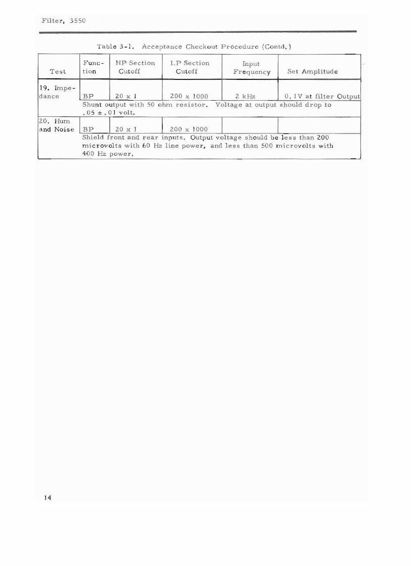
19. Impe dance B P 2 0 x I 200 x 10 0 0 2 k Hz O. I V a t filter O u t pu t
S hun t ou t p u t with 50 hm re si stor . Voltage a t output s h oul d drop t o • as ± • a1 v olt .
2 0 . Hum a nd Nois e B P 20 x I 200 x 10 0 0
Shield fron t a n d r e a r inp uts . Ou t put v olta g e should b e l e s s t h a n ZOO m i c r o v olts with 60 Hz l i ne powe r , and l e ss than 50 0 m i c r ov ol t s w i t h 4 0 0 Hz power .
14
Section 4 - C ir cuit De s c r i tion
SECTION 4
CIRCUIT DESCRIPTI O N
4.1 GENERAL
Figure 4 - 1 s hows the M od el 35 50 fi lte r in bloc k d i ag r a m pr e s e nta ti o n .
T h e incoming signal passe s fi rst th r ough the unity-gain input amplif i e r and t h e n is sw i tc h e d b y the Function Sw i t c h eithe r t o the High Pas s ( HP ) or t h e Low P a s s (L P) se c t i o n or both, depending on t h e f i lte ring function s e l e c t e d . In the Band P a s s p os ition bot h s e c ti ons a r c o n n e c t ed in s e r i e s , In the Band R e j e c t p o s i t i o n b o t h se c t i o n s a r e in parallel w i t h o u t p uts added t h r o u g h a pai r of 10k resisto r s .
The output amplifie r is cap ac i t o r co upl e d, to e lim in a te d c d r i f t fro m the pr e v i o u s stage s , and p rov ide s low o u t p u t im p edance . It a l s o ha s v oltag e g ain to compens a t e for adding l o s ses and t o maintain z e r o insertion l o ss in the Band R e j e c t (BR) ftlIlCt i o n ,
T h e f oll o w in g parag raph s d e s c r i be eac h section of the Mod e l 3 5 50 filter more fully.
4.2 INPUT AMPLIFIER
Each of t h e I PUT c on ne c t ors, f r on t a n d r e a r , ha s a r es i s t o r i n s e r i e s . Wi t h t h e capacitance of the sh ielded f r o n t - t o - rear c a b le the s e r e s i s t o r s a c t a s l o w p a ss fil te r s , at te n ua t ing f r eq ue n c i e s above 2 MHz.
The i nput capacitor C I OI , b l o ck s d c and w i t h HIO I prov ide s a l o w f r equen c y p a s s b a n d d ow n t o 0 . 2 Hz . Resi stor R I 0 2 pr o t e cts t h e inpu t F E 010 1 ( r om d a m a g e b y high input v ol t a g e s. C I 0 2 and R I 0 3 a r e h igh - f req u enc y b y pass for R I 0 2.
The d rain 0 [ 0 10 1 dr ive s the b a s e ofOI02. The c ollector of 010 2, t hr o ug h di ssipa t i o n limiting r e s i s t or R II 0 , p r ov ide s t h e output s ig n a l , as w e ll a s fe e d b ack t o the s o u r c e of 0 10 1. R e s i s t o r RI 0 4 , c a p a ci t or C I G3 and t he ferrit e b ead LI O I are fo r loop stabilization.
4.3 HIGH PASS SECTION
In put t o t h e Hi g h Pas s Section comes f r om t h e i n put l o o p through t he fu n c t i on s w i tch. It goes dir e ctly t o th e firs t H P t un i n g n e twork con s isting o f t w o p o tenti o m ete rs and tw o c a pa ci t o r s. T he poten t i ome t e r s a r e ganged, a r e o p e r a t e d b y the tuning d ial , and hav e s e r i e s and pa rall e l tr im m i n g r e s i s t o r s . The c a p a c it o r s a r e sele c t ed by m e a ns of the b a n d s w i t c h . T h e v a l u e s o f the tw o network
15
CII 0
IHIGH PASS SECT ION I FUNCTION
SWITCH
LP HP,---£=BP
;4(1 ::4(; I ~~g~ > f Jr , I ~~g;
.#1° I 1°
0203IN PUT 1-1_ AMPLI F IER I
INPUT 'rJ I.... . CIt:. 0-1c
o-r Ic:> J>. I I
I tIl - ' 0 rl- -- ~~-e--+---+--~if'v~~VXf\r"'--i 0 30 1 C1
1° °'1""
0.'. IPJ Otl '1 PJ
3 1° 1r -
L I ---1
:1 ° IL- --
OUTPUT AMPLI F IE R
0302
0303
IL8W1I
0306~ - I
I
0304 0 30 5
-I I
RESPONSE SWITCH
I I I IMA X
FLAT .
'rJ..... .......... '1
VJ V1 V1 o
Section 4 - Cir c u i t De s c r i p t i o n
capacitors are in the r atio of 10 to I , so tha t e a ch capa c i t o r c a n be us e d on two adjacent band s . A doubl e em i t ter f ollo wer, Q 20 I and Q 20 2 a t the output of the n e t w o r k pr ov ide s i s ol a t i on and drives, through a v olta g e divider R205-R206 , t h e fe e d back emitter followe r 0 20 3.
The ci r c u i t s o f a r comprises the fi r s t I I quadratic" of the HP sec t ion . T he n a me " q u a d r a tic" is u s e d her e t o .de not e a n e t work wi th a s e cond o r de r transfe r func ti on , a s i n this c a s e:
E 2 S 2
= E 1 1 + 2 a s + S2
where s = f fa
f = frequency
f o = 1
a =" pe aki n g fac t o r "
The II pea kin g fa c to r!' d epends on the r a t i o s of n e twor k re s is tors a nd c a p a c i t o r s and t he amount of feed back . F o r the tw o valu e s of " a" us ed in the Mod e l 35 50 , irequency response s of the two quad ratics wo uld look like th i s :
+5
o
~ -5 z o i= -10 e:( => z W-1 5 l-I-e:(
-20
-25
~ ....~ "V = 0 . 3B3 a
~
r- r--i""-- >F:: ~
~~V r-. a=SUM V
,,~a=0.92.:11-
\~~
\ '\ \ 1\
.1 .2 .3.4 .6 .B I 2 3 4 6 B 10
NORMALIZED FREQUENCY
F ig u r e 4 - 2 . Res pons e of Q ua d r a tic Arn pli fi e r s
The second HP q u a d r a ti c i s s lightly different ; an amplifier 0 2 0 4 and Q 2 05 feeds the s e cond R C, w hich in turn fe ed s the F E T-in pu t a m plif i e r Q 2 0 6, 0 207 . Resistor s
R 2 l8 and R22 6 and R2l9 , c on n e c t e d as a v o l t a g e divide r , dete rmine the gain of the loop. Res istors R2l8 and R226 are paralleled on Band 4 with R7 0 l a nd o n band 5 w i t h R 7 0 2 to inc r ease the a mplifi e r gain.
17
Filte r , 35 5G
The feedback emitter followe . 020 8 i s fed f r om t h e loop output through d ivider R22 ] - R 2 2 5. On b a nd 4 t h e feedback i s modified b y R704, and on b a nd 5 by R 70 5, C 74 0, C 7 4 1.
The R E S P O NS E s wit ch s h unts R 2 2 5 with R 22 2 in the L OW 0 po s ition . This r e d u c t i on of fe e d ba ck changes the p e a king fa c t o r o f t h e s e c ond qu a d r a t i c from a = .3 83 to about a = . 9 7, chang ing t he res p onse of the High P a s s s e c t i o n from a Bu t t e r w o r t h t o t he damped, tr a n s ien t- f r e e for m di s c u s sed i n Se ction 2. 4 . 3.
4.4 LOW PASS SECTION
The L ow P a s s s e c tion consis ts of two quadrat i c s , same a s the Hig h P a s s s e c t i on de s c r ib e d in 4 .3. The fir s t amplifie r consists of 0 30 1 and Q 30 2, connec t e d as a d o u bl e e m i t ter f ollow er . Inductor L 30 2 a nd R3 19 in the emitt e r of Q 30 2 prevent s p u r iou s hig h f r e q ue n c y o s c ill a t ion . Volta g e d i v ide r R 305 - R3 0 7 p r ov id e s feedback a mpli fi e r Q3 0 3 w i t h t he p r op e r gain to ob t a i n a peaking fact o r o f a = .924, as req u i r e d for the fir s t q u a d rat i c of a four - pole Butte r w o r th fil t e r .
The am plifi er f o r th e se c ond qu a d r a t i c , Q 304 , Q30 5 and Q 3 0 6 i s s imila r t o t h e f i r s t o ne . The h i g h e r pe ak i ng fa c t o r o f t h i s q ua d r a t i c (a = .3 83, same as the H ig h Pas s se c on d q ua d r a tic) r e qu i r es m o re fee d b a c k s o the d i v id e r R 3 13 - R 3 18 h a s l ess a t t en u a t i on .
R ESPONSE switch S901 B, when s w it c he d t o the L O W 0 pos i t i on, c h a nges the peak ing fa c t o r of this quadrat i c fr om a = .383 to a ' = . 97 by swi t c h i ng R317 from shu ntin g R313 to s hu n t i n g R3 16 .
4.5 OUTPUT AMPLIFIER
The ou t pu t ,a m plifi e r i s capa c itor coupled a t the in p ut (C401 and R404). T h e cutoff i s at a bout 0. 2 Hz - - - sam e as fo r t he input amplifi e r . The fir s t s t a ge, Q 4 0 1, a n F E T , drives the o u t p u t s tag e 0 403 t hro ug h t h e emitter followe r 0402. R4 12 i n the colle c tor of 0 40 3 limits dissip ati on ; C40 8 is a high f r equ e n c y b y pa s s . L401 a nd R 4 10 in s e r i e s with the ou t pu t s tabi liz e t h e l o o p for c a p a ci t iv e l oa d s . C R40 I i s f o r t e m p e r a t u r e com p ensation of t he outp u t DC lev e l.
Feedb a ck to t h e s our ce of t he input FET c om es d i r e c t l y f r om C R 40 1 in the L P, HP, and BP mode s . In the BR mode signals fr om the High P a s s a nd the Low P a s s s e c t ions a r e add e d through re sis t o r s R 80 2 and R803 , w it h a 6 d B los s o f gain. To mak e
u p fo r t h e 10s 6, a r e si s t a n c e d i v ide r R80 S a nd R8 0? and R 413 i s in s erted in the fe e dba ck , c a u s ing a 6 d B i ncre a s e i n t h e ampl ifie r g a i n .
Output d c l eve l i s adjusted c o a r s e l y with P401 on the p r int e d circui t b oa r d , and can be fin ely tr immed wi t h P90 1 in the rear panel. In the B R mode o nly, the level can be set w i th P 402.
4.6 POWER SUPPLY
T h e p o w e r s u p ply p r ovid e s + 15 vol t a nd - 15 volt regula t e d v olta g es fo r t he ope r a tion of the Model 3550 . The uni t can be ope r a t e d either from 10 5 to 12 5 volt or a 210 to 2 50 volt a c s ou r c e , 50 t o 40 0 Hz. T h e two line vol ta ge s c a n b e a c commod a t e d by
18
Section 4 - C i r c u i De s cr iptio n
u s e rJ f t h e II SV /230V LIN E s w it c h , located on the rear pane l. A fus e , a powe r s witc h, a nd an indicator lamp with i t s s erie s r e s i s t o r c o m p l e te the primary c i r c u it
f t h e power t ra n s fo r me r . T he c enter tapped s econdary drives a dual full wave r ecti fi er , providin g both po s i ti ve and n e gative outputs . The s e are smoothed b y fiIt er c a p a ci to rs GSO I and C S02, and then s epa rately regulated. Each r egulato r i nc orporate s a s e r i e s t r a n s i s t o r , an a rnpl i fi e r , and another transistor used as a Z e n e r r e fere nc e . T o understand the operation o f t h e r e g u l a t o r s , conside r the p ositive supply a s follows :
Any vi r t u a l di s turbance, sayan increase in + 15 regulated voltag e , w oul d be a pplied to the emitter of Q503 through t h e Ze ne r Q50 2 and t e m p e r a t u r e compensating diodes C R S0 2 . T he base of 0503 w ould a lso get a s ig n a l in the same direction but at tenuated by the v ol tage divider R SI I and R 5 0 1 - R S0 6 . A s a r e s u lt , Q 5 0 3 w o ul d be u rned off , r educing the base c u r r e n t of Q 50 1, t hu s lowe ring the o utput v o l t a g e of the r e gu l a t o r . T h e operation of the negative p owe r s u p p ly i s a n a l o go us .
apacito r s C50 3 and C504 s p e e d u p the operation of the regulators b y k eeping b a ses o f Q 503 and Q504 steady wh e n fast changes of regulator ou t p u t are fe d to their e m i tt e rs . R 50 8 and C50 8 in parallel fe e d some ripple from the unregulated suppl y into the regulator base , in the prope r phase, to reduce ripple on the regulated n e g a t i v e output; R 50 5 a n d C50 7 do the same for th e po sitiv e pow e r s u p pl y .
19
Fil te r , 3 550
SECTION 5
MAINTENANCE
5.1 INTRODUCTIOH
If th e M od el 3 5 50 i s n o t fnn ctioning properly a nd r e q u i r e s s e r v i ce , fullow this pro c e d u r e t o l o c a t e t h e SOUJ'c e o f t r o ubl e , To o b ta i n a r c e s s to the i n t e r io r of t h e fil ter , r e m o v e the screws centered at t he r e a r o f each ,:o \"e r: s l iding u ti t he s id e c o v e r s will unlock t he r op and o t t orn c o ve r s ,
T he gen e ral l ay o u t of m ajo r com pon en ts , t e st po in t s , s c r e wd r iv e r c on t r ols and adj u s t m e n t s a r e s ho w n i n Figu r e 5 - 1. A de tailed c orn pone n t layout for t h e printed c ir cui t card is in cluded w i th t h e sch e m a ti c diagram a t the end of t h i s b o ok . Var i o u s c h e ck po int s a n d vol t age s a r e s h o wn on the sc he m a t i c d i ag r arn a nd ar e a lso marked on th e p rin ted c ir c u i t c a r d ,
F ir s t m a k e a v i s u a l i n s p e c t i o n ; c h eck t h e u n i t f o r s u ch t h i ngs a s b r o ken wi re s . burn t o r l oos e compo ne n t s , o r s i rn i l a r cond i tions wh i c h c oul d cau se troub l e . An y t r o u b l es hoot i ng of t he F i l t e r w ill b e greatly s i m plif i e d i f y o u under stand t he ope r at io n o f t he c i r c ui t. B e fore atte mpting de t a i led troub leshoo ting r e fer t u C i r c u it Des cription Se ti o n 4 ,
5.2 POWER SUPPLY
U the f il t er doe s n o t see m t o b e w o r k i n g p rope rl y, c hec k the two p owe r supplie s fir st . If t h e p o s i t i v e a nd n e g a tive 15 v olt s u p pl ies app ea r t o b e c o r r e c t r e fer a signal t r a c i ng a n a lys i s , p ar a g r a p h 5 .3 . An y malfun ct i on o f t he p ower s u p pl i e s will g e n e r a ll y c a u se a large e rro r i n pos it i v e o r n e g a t i ve 15 v olt outp ut. Small e r r o r s m a y be co r rec ted by a dju s t i n g RS06 and R 509 r e spe c t i vely . If t h e - 15 volt supply is c orre c t and the + 15 volt suppl y is in c o r r e c t, check t he r e fe r e n c e v oltage f r o m t h e emi tte r o f Q 50 3 t o t h e coll e c t or of 0 50 2 . T h i s r e fere n c - v olta g e shou l d b e 8.4 ±. 5 v o l t s . orm a ll y , if th e + 15 volt s u p pl y is hig h, t h e b a se emi tte r vo l t a g e of 0 50 3 w ill b e reduced , de c re a s i n g i t s c oll e ctor c u r r e nt, l o w e r ing the emi tte r t o a s e voltage a n d t u r n ing o ff 0 50 I . T hi s w ill increas e the emitter t o c oll e c t o r v olt a g e o f 0 501 , co r rec ting the + 15 v olt s u p pl y . The fa ilure w ill b e fo un d w her e thi s a c t io n is b locked , if t he + 15 v olt suppl y is l o w , t h e c u r r e n t in Q 50 3 w i l l b e inc r e ased , tu r n in g on Q50 I . if t he s u p pl y v c l t ag e i s 10\'1 and Q 5 0 '~ and 0 50 I a pp e a r t o be o pe rati ng p r o pe rl y , t h e c au s e i s m o s t like l y exce ss ive c u r r e n t. in the m a i n f ilte r s e c t ion . An in c o r r e c t - 15 v olt s u p pl y may be t r a c e d i n a s im il a r manne r .
20
Se ction 5 - M a i ntenanc e
CI02
I I
I I
C707
G727
R702 C717
C737
\ / \ /
\ /
IUJ ~ ~
SIDE VIEW
C741
G507
-~
F i g u re 5 -1. T r i m s a nd Adjustm e nt s
21
F ilter, 3550
5.3 SIGNAL TRACING ANAL YSIS
If the p o w e r s u pp l i e s appea r t o b e c o r r ec t but the Mod e l 3550 i s n o t w orking , the following signal tracing analys is should help locate the a r e a o f malfunction. Set the F u n c t ion Swit c h t o BP; set th e R E S P O NSE s w i t c h to L O W 0 po sition . Se t both the l o w and high c u t off frequ encie s t o 20 0 Hz . C o n n e c t a 2 0 0 Hz 5 - v ol t rm s sine wa v e s i g n al t o the in p u t term inals . If the t e st signal does not appea .- o rrectly at the o u t p ut, the a r e a of the malfunct i on m a y b e localized b y detennin ing whe r e in the F ilte r th e signal fi r st dev iates from t h e normal.
Table 5 - J sho w s v a r i o u s te st p oints with their c o r r e c t sig n a l l e vel s for band pas s o pera t i on . If a test point is found w h o s e signal l evel differs a p p r e cia b l y f r o m the c o r r e c t value, t h e ci r cuit r y im m e d i a t e ly p r eceding t h a t te st point s hould b e car e fully checked .
Inp u t: 5 vrms, 2 0 0 Hz L P d ial : 200 x 1 HP d i a l : 200 x 1 F un c t i o n : B P RES P O NS E : L O W 0
5.4 TUNING CIRCUITS
If sig n al traci n g shows one of the tuning circuits to b e faulty , it s h ould be determined i f t h e trouble i s in t h e r e s i s t i v e or capac itive e lements . If t he trouble is in a c a p a citiv e element used on l y i n the l ow e s t o r highest multiplie r r a ng e , the mal f unc t i o n w ill appear on l y on these pos itions . E a c h of the other tuning capacitors , if de f e c tive , w i ll in t r od u c e an e r r or in two adjacent bands . If there i s a problem In a r e s i s t i v e element, the trouble w ill be of a general nature and w ill s h o w u p on all mul t i pli e r b a n d s .
22
S e c t i on 5 - 1v1a i n t e n a n ce
The alues of capacitance used on the highe s t b a nd are sele c t ed t o compensat e f or stray c a p a ci t a n c e and are therefore no t c om pl e t e l y in decade r a t i o s of those us ed on the l ow e r bands .
E a c h o f th e v a r i a ble r e s i s t a n c e element s consist s of fou r p o t e n t i om e te r s ganged t o gether w i t h a gear assembly. Each p oten ti om e te r has s e r i e s a n d s h un t trims t o i n s u r e pr oper t r a c k i ng . The t ri m s and the a ng ul a r o rientation of the p o t en t i orn e te r s are c a r e fully ad justed at the fa cto r y . If it becomes neces sary to c h ang e on e of the s e potentiometers i n th e fie l d , i t should be r e pl a c e d only w i t h a u n i t s u ppli e d by th e f a c t o ry c om pl e t e wit h proper t r i m s . T he a ng ula r orien t ation s h ou l d t h e n be ca r e full y adjusted foll o w ing the procedu r e suppli ed with the pa r t s .
23
Filte r , 3 5 50
SECTIO N 6
CALIBRATION AND ADJUSTMENT
6,1 INTRODUCTION
Before any adjustments the procedure in Section 3 should be followed to dete r rn i n e i f adjus tments are n e c e s s a r y . The following procedure i s provided f or t h e a d j u st men t and c a lib r a t i on o f the fi lter in the f i eld, and adherence to this procedu re should restore the filte r to its orig inal spe i fi c at i on s , If any difficulties are encountered, please refer t o T roubleshooting , Section 5. If any uestion ari ses w h ic h are not c o v e r e d b y this procedu re, please COntact our factory service depar tment. T h e location s of t r irn s a n d adj us trne rit s a r e s h own in F i g u r e 5 - ] . The test p o i n t s are m ark ed on the P C board.
A c c e s s to t h e in t e r i o r o f th e M od el 3 5 50 is gained by remov ing t h e s c r e w centered a t t he r e a r o f each cove r; sliding o ff the side overs w i ll unlock the to p a nd b o t tom cove r s .
6.2 TEST EQUIPMENT REQUIRED
T h e f oll ow i ng t e s t e qu i pment IS requi red t o per fo rm t h e se test s.
a . R C O s cill a t o r , w i t h fr eque nc y r a ng e 0 . 0 1 H z to 1 MHz, f r e q u e n c y accuracy ±O. 50/0 to 100 kH z , f r e q u e n c y r es p ons e bet te r tha n ±O. 5 db a nd d is t o rtion l e s s t h a n 0 .02%, Krohn-Hite Model 4 10 0A or equ i v a le nt .
b . Os c i llo s c o p e, w i t h DC to 50 MHz b a n d width , ve r t i c a l input sens it iv i t y of 1 m v/cm, T ektronix typ e 5 4 4 , w ith t ype l A 5 p lug-in , o r e q u i valent.
c. AC Voltme t er , c a p a bl e o f m e a s u r in g 100 microvolt s t o 10 vo l t s RMS , Balla n t in e Mod e l 3 14A or e qu i v a l e nt.
d. DC Volt m e t er , capable o f m e asur ing 1 m.ill i volt t o 20 v o lt s , F l u k e M od e l 8000A or e qu i v a l e nt.
e. Va r i a b l e aut o -tra n s form e r fo r ad justing li n e v olta g e .
24
Secti o n 6 - Ca lib r at i on a nd Adj u s t m e n t
6.3 INITIAL SET·UP
a. Set function switch to BP
b. Set low pass dial to 60, multiplier to x l O
c. Set high pass dial to 60, multiplier to x l O,
6.4 POWER SUPPLY
a. Short filu~ r input.
b. Connect d-c voltmeter betwe e n g r ou nd a nd + 15 volts (red lead on P90l).
c. Adjust R506 for l5"±O. 2 volts.
d. Co nn ect d-c v oltm e t er betw e e n gro u nd a nd -15 volts (g r ay lead on P90l) .
e . Adju st R 50 9 for -1 5+0.2 volts .
6.5 OUTPUT DC LEVEL
a. Con n e c t d-c voltmeter to output. Set P90 l to midrange .
b. Adjus t P 4 0 1 fo r 0 v o lt s on the fi lte r o u tput .
c . Switch function s witch to B R .
d. Adjust P402 for 0 vo lt s o n fi lte r output.
e. Ren~ovc short fz o n i input.
6.6 CALI BRATlON PROCEDU RE
The calibration proc e dure i s give n i n Table 6 -1. In t he tab l e , t h e i n i tia l t e st setu p is g i v e n i n t a b u l a r fo r m a t the b e g i n n i ng of ea c h t e s t , and then foll ows a s e qu e nc e o f steps. It i s importa nt t h at the seq u e n c e be followed i n ord er. Nomi n a l o s cill a t o r output vo lta g e a t t h e b eg in n i n g of all tes t s is 1 volt r m s , Amplitu d e is then adjusted a t the t e s t point g ive n . Unless o t herwise s p e c i fi e d , voltag es are rms.
25
- - - --
- - - - -
- - - --
-----
- -- - -
- - - --
-- - --
- - - --
Filter, 3 5 50
Tabl e 6- 1. Calibrat i on P r ocedure
Input T e s t F un c t i on H P Se ction LP S e c t i on F r eq . Set Amplit ude
1. LP Dial Set L P 6 0 x 10 50 Hz J V a t output S wi t ch os c to 12 00 Hz . Adj u s t L P dial f o r r e a d i n g of 6 3 m ill i v olts on a cvrn , LP dial s h ou l d r e a d 60 . H off, l oo sen d ial s e tsc rews and se t to 60 . Tig h ten .
2 . L P Cutoff Re spon se LP 6 0 x 10 ZOO Hz I V a t o u t p u t
Swi t ch o sc f rom zoo Hz to 600 Hz . Ou tput s h ould read . 6 3 t o · 77 v olt .
3. LP x 1000 LP 6 0 x 1000 IVatTPI 8 Switch o s c fr om 6 k Hz to 4 8 k Hz . Tr im C72 7 f o r . 96 v olt at T P I8 . Switch o sc to 60 k Hz . T rim C 7 3 7 for 0 . 7 v olt at TP1 8. If any a djustments were made, r e pe a t ste p 3 .
6 k Hz
4 . HP D ia l Se t 60 x 10 I V at output Switch o s c to 300 Hz . Adju st HP dial for reading of 6 3 milli v o l t s on a c v m , H P d ial should indicat e 6 0 . Hoff , l o o s en d ial s e tsc r e w s and se t t o 60 . Tig h te n setscrew s.
HP 6 k Hz
5 . HP x 10 Unity Gain HP 6 0 x 10 2 kHz I V at i n pu t Connect a cv rn t o o ut p u t. Ad ju s t R226 fo r • 96 to 1. 04 volts .
6 . HP Cu t off R e s ponse HP 60 x 10 2. kHz 1V at output
Switch osc from 2. k Hz to 600 Hz . Output s h ould r e a d . 63 t o · 77 volt . H out of l imits , tr im R22.5 for. 7 ± . 0 7 v olt .
7 . H P x 10 0 0 C a p a ci t o r Adjus t 20 x 1000 reo kHz I V a t T P 4
7 a ) At 100 kHz s e t I v olt at TP4 . Switch o sc from 100 k Hz to 5 kHz . Volt a g e a t TP4 should d r o p to 63 millivolts . If off t r i m C7 0 7 . If C 707 adj u s t m e n t i s nece s sa r y repeat s t e p 7a .
HP
7b) Con n e c t a cvrn t o o u t p u t . Swi t c h o s c t o 100 kHz . Adjust in p u t fo r 1 v olt a t output . Sw itch os c t o 10 k Hz . O u t pu t s h ou l d r e a d 45 to 80 mill ivolts . If off adjust C7 17 . If C 7 17 a dju s t m e n t is necessa r y. r e p e a t s t e p 7b.
8. 2 0 0 k Hz Ca l i b r a t i on ZOO x 10 0 0 60 0 k Hz 1V at output
Sw i t c h osc from 600 k Hz t o 2 0 0 k Hz . Trim C 74 ] fo r . 63 t o H P
• 77 v olt at output .
9. Ban d R e j e c t ] 00 x ]100 x 10 BR 3k H z 1V at input
R e m o ve a c vrn f r o m input and con n e c t to o u t p ut. A d ju s t R 4 13 for. 96 t o 1. 04 vo l t s a t o utput.