18
Operational-Amplifier and Data-Converter Circuits

Operational-Amplifier andData-Converter Circuits
Outline
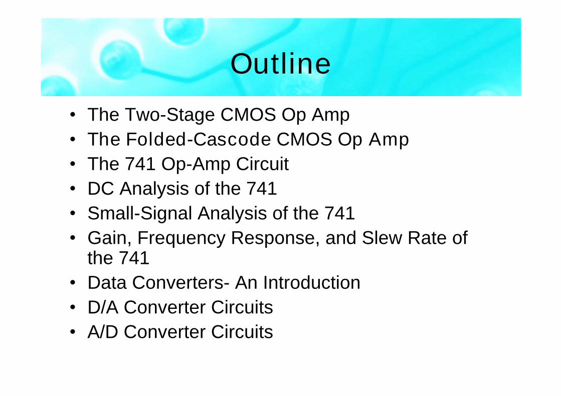
•The Two-Stage CMOS Op Amp•The Folded-Cascode CMOS Op Amp•The 741 Op-Amp Circuit•DC Analysis of the 741•Small-Signal Analysis of the 741•Gain, Frequency Response, and Slew Rate of
the 741•Data Converters- An Introduction•D/A Converter Circuits•A/D Converter Circuits

Input & Output Ranges
Output swing:
Input common-mode range:

Rail-to-Rail Input OperationIncrease the input common-mode range

The Wide-Swing Current MirrorIncrease the output voltage range

VBIAS Generation
1) Q5 has a W/L ratio equal to ¼ that of the transistorsin the wide-swing current mirror
2) Same IREF utilized in both circuits

Outline
•The Two-Stage CMOS Op Amp•The Folded-Cascode CMOS Op Amp•The 741 Op-Amp Circuit•DC Analysis of the 741•Small-Signal Analysis of the 741•Gain, Frequency Response, and Slew Rate of
the 741•Data Converters- An Introduction•D/A Converter Circuits•A/D Converter Circuits
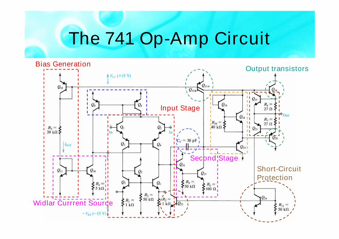
The 741 Op-Amp CircuitBias Generation
Widlar Currrent Source
Short-CircuitProtection
Input Stage
Second Stage
Output transistors
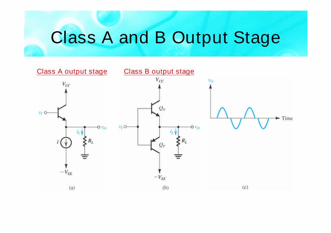
Class A and B Output Stage
Class A output stage Class B output stage

Class AB Output Stage

Outline
•The Two-Stage CMOS Op Amp•The Folded-Cascode CMOS Op Amp•The 741 Op-Amp Circuit•DC Analysis of the 741•Small-Signal Analysis of the 741•Gain, Frequency Response, and Slew Rate of
the 741•Data Converters- An Introduction•D/A Converter Circuits•A/D Converter Circuits
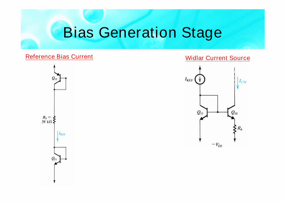
Bias Generation StageReference Bias Current Widlar Current Source
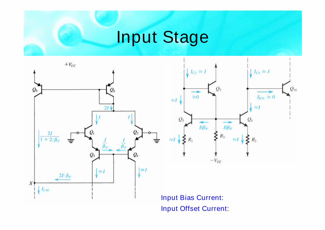
Input Stage
Input Bias Current:
Input Offset Current:

Second Stage

Output Stage

Outline
•The Two-Stage CMOS Op Amp•The Folded-Cascode CMOS Op Amp•The 741 Op-Amp Circuit•DC Analysis of the 741•Small-Signal Analysis of the 741•Gain, Frequency Response, and Slew Rate of
the 741•Data Converters- An Introduction•D/A Converter Circuits•A/D Converter Circuits

Input Stage
Rid = Gm1 =

Small-Signal Equivalent Circuit
Ro1 =
Output Resistance


