Page 1 of 15 University of North Carolina at Charlotte Department of Electrical and Computer Engineering Laboratory Experimentation Report Name: Ethan Miller Date: May 22, 2014 Course Number: ECGR 3155 Section: L01 Experiment Title: [1] Operational Amplifiers Lab Partner: None Experiment Number: 1 Objective: The purpose of this experiment was to examine a linear integrated circuit, the operational amplifier (op-amp). During this laboratory there was a observant of AC/DC amplification, input, and output impedance. Equipment List: Items Asset # MB-106 Breadboard 00000001 220Ω 00000002 10KΩ 00000003 100Ω 00000004 1KΩ 00000005 .1μF 00000006 10μF 00000007 AFG310 Arbitrary Function Generator 00056789 Agilent InfiniiVision 2000-X Series Oscilloscope 00087890 E3612A Power Supply 00012457 Agilent 34461A 6 ½ Digital Multimeter 00136896 Relevant Theory/Background Information: Operational amplifiers (op-amps) have been known to be useful devices. These amplifiers are called operational because the use of math operations to have an output of a voltage or current. The following are a list of different operations of op-amps: amplifiers, attenuators, summers, integrators, differentiators, filters, oscillators, non-inverting and inverting, difference, and instrumentation Op-amps are designed to sense the difference between the input signals. The output signal of an op-amp has a value very large compared to the difference of the two input signals. The gain of the circuit was determined by Equation 1. The response for the op-amp has used a direct-coupled differential amplifier feedback control characteristic.
Transcript
Page 1 of 15
University of North Carolina at Charlotte
Department of Electrical and Computer Engineering
Laboratory Experimentation Report
Name: Ethan Miller Date: May 22, 2014
Course Number: ECGR 3155 Section: L01
Experiment Title: [1] Operational Amplifiers
Lab Partner: None Experiment Number: 1
Objective:
The purpose of this experiment was to examine a linear integrated circuit, the operational
amplifier (op-amp). During this laboratory there was a observant of AC/DC amplification, input,
and output impedance.
Equipment List:
Items Asset #
MB-106 Breadboard 00000001
220Ω 00000002
10KΩ 00000003
100Ω 00000004
1KΩ 00000005
.1µF 00000006
10µF 00000007
AFG310 Arbitrary Function Generator 00056789
Agilent InfiniiVision 2000-X Series Oscilloscope 00087890
E3612A Power Supply 00012457
Agilent 34461A 6 ½ Digital Multimeter 00136896
Relevant Theory/Background Information:
Operational amplifiers (op-amps) have been known to be useful devices. These amplifiers
are called operational because the use of math operations to have an output of a voltage or
current. The following are a list of different operations of op-amps: amplifiers, attenuators,
summers, integrators, differentiators, filters, oscillators, non-inverting and inverting, difference,
and instrumentation
Op-amps are designed to sense the difference between the input signals. The output
signal of an op-amp has a value very large compared to the difference of the two input signals.
The gain of the circuit was determined by Equation 1. The response for the op-amp has used a
direct-coupled differential amplifier feedback control characteristic.
Page 2 of 15
(Direct-Coupled is amplifying the DC with a time varying signal) The customary symbol
for an op-amp is shown in Figure 1. Where the input pins are 3 and 2, output pin is 1, and the
voltage rails are pins 8 and 4. Non-inverting and inverting op-amps represent the positive and
negative terminals.
Figure 1: Op-Amp Symbol
A single stage amplifier has been built with one transistor; however the gain of a single
stage amplifier were often inadequate. This is solved by cascading with a NPN and PNP
transistor to balance out the temperature effects, plus other considerations were involved.
Multistage amplifiers were built with a single chip, using an integrated circuit (IC). Advantages
of an IC have been known for the following 1) improved noise immunity, 2) superior frequency
response, 3) stability, 4) low power consumption and 5) low cost.
The output voltage of an op-amp has been known for the difference between the input
voltages multiplied by its open loop gain. The gain was denoted by . The effect of a finite was
denoted as . When the positive input terminal was grounded there was a negative gain
otherwise known as an inverting op-amp. Thus the current through the op-amp was now found,
and shown in Equation 2. Ideal op-amps are defined by the following parameters 1) no or very
little current is drawn into the op-amp, thus the positive and negative terminals have 0 amps, 2)
the input impedance was infinite ( , 3) the output impedance was 0 ohms. In order for the gain
to be finite at the output the difference between the two input signals has to be 0 volts. A virtual
short is the voltage at the positive terminal will appear at the negative terminal. A virtual ground
is the voltage at the negative terminal having a 0 voltage, but was not physically connected to
ground. Ideally the gain was assumed to be infinite, as shown in Equation 2, and as the gain
approaches infinite the ratio for the gain was found by the ratios of the feedback resistance (
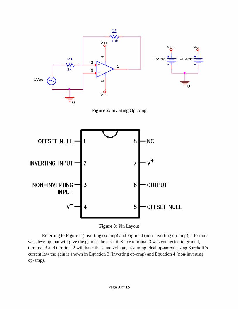
to the input resistance ( . An inverting op-amp is shown in Figure 2. [1]
LM741 op-amp was used in this experiment has a dual in-line package called DIP. Op-
amps have two ways to anguished from top of the op-amp, which are notches or dimples. The
pin layout for the IC is shown on the datasheet. The pin numbers usually start at the 1 from the
notch or the dimple and go to the end of the IC, usually to pin number 8. An op-amp pin layout is
shown in Figure 3. Shown in Figure 3, are a set of pins called null-offset, which are set to 0 volts.
In the case of the IC does not have a gain output of 0 volts, the null-offset needs to be set to
ensure that the op-amp was ideal.
-
+3
21
84
Page 3 of 15
Figure 2: Inverting Op-Amp
Figure 3: Pin Layout
Referring to Figure 2 (inverting op-amp) and Figure 4 (non-inverting op-amp), a formula
was develop that will give the gain of the circuit. Since terminal 3 was connected to ground,
terminal 3 and terminal 2 will have the same voltage, assuming ideal op-amps. Using Kirchoff’s
current law the gain is shown in Equation 3 (inverting op-amp) and Equation 4 (non-inverting
op-amp).
-
+3
21
84
R1
1k
Rf
10k
0
0
V--
V++V--V++
15Vdc -15Vdc
1Vac
Page 4 of 15
Figure 4: Non-Inverting Op-Amp
(Eqn.1)
(Eqn.2)
(Eqn.3)
(Eqn.4)
-
+3
21
84
Rf
10k
0
V--
V++
V--V++
15Vdc -15Vdc
1Vac
0
R1
1k
0
Page 5 of 15
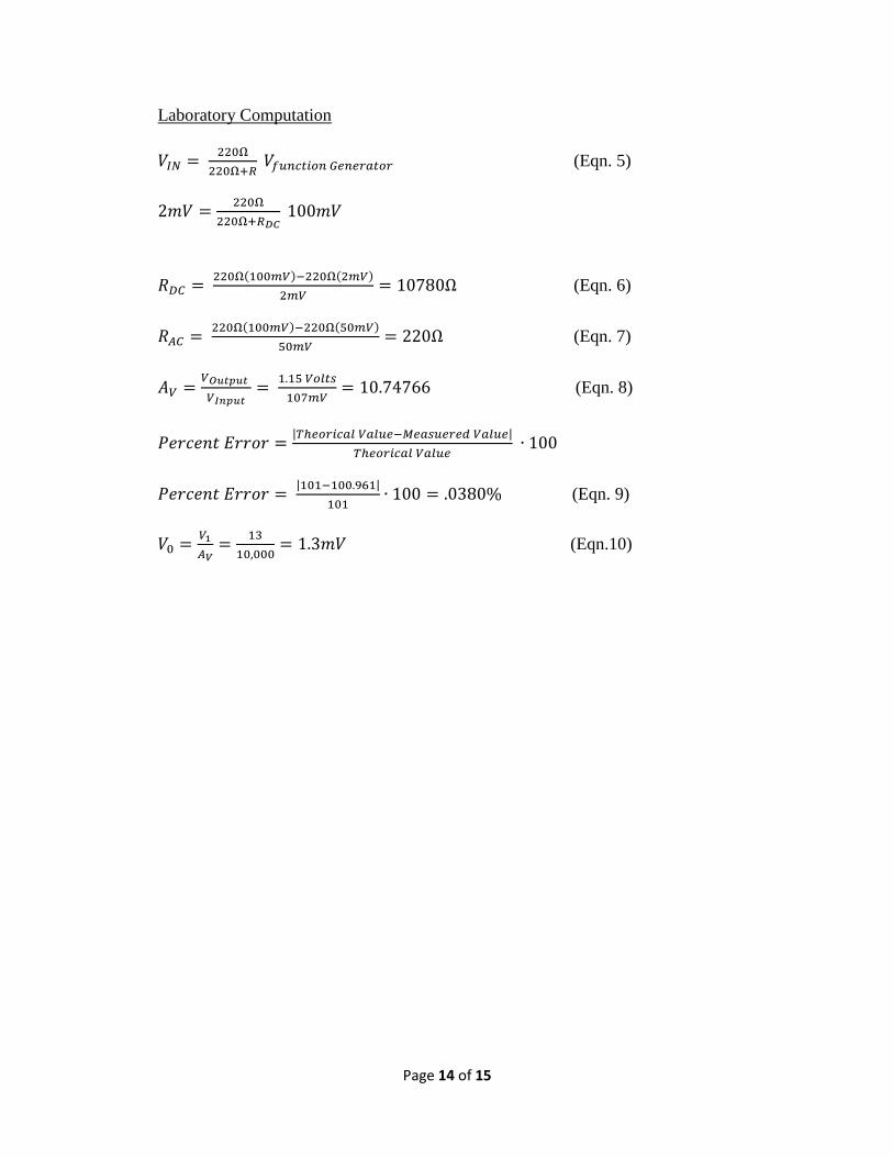
Experimental Data/Analysis:
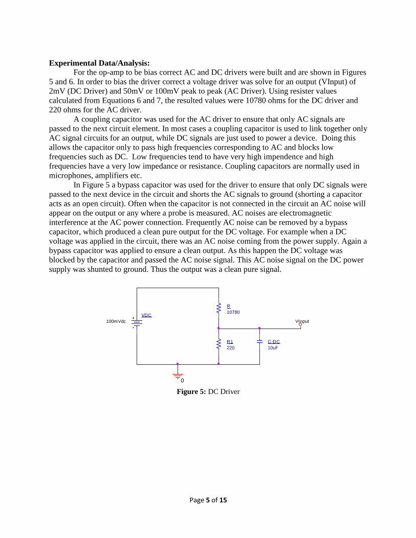
For the op-amp to be bias correct AC and DC drivers were built and are shown in Figures
5 and 6. In order to bias the driver correct a voltage driver was solve for an output (VInput) of
2mV (DC Driver) and 50mV or 100mV peak to peak (AC Driver). Using resister values
calculated from Equations 6 and 7, the resulted values were 10780 ohms for the DC driver and
220 ohms for the AC driver.
A coupling capacitor was used for the AC driver to ensure that only AC signals are
passed to the next circuit element. In most cases a coupling capacitor is used to link together only
AC signal circuits for an output, while DC signals are just used to power a device. Doing this
allows the capacitor only to pass high frequencies corresponding to AC and blocks low
frequencies such as DC. Low frequencies tend to have very high impendence and high
frequencies have a very low impedance or resistance. Coupling capacitors are normally used in
microphones, amplifiers etc.
In Figure 5 a bypass capacitor was used for the driver to ensure that only DC signals were
passed to the next device in the circuit and shorts the AC signals to ground (shorting a capacitor
acts as an open circuit). Often when the capacitor is not connected in the circuit an AC noise will
appear on the output or any where a probe is measured. AC noises are electromagnetic
interference at the AC power connection. Frequently AC noise can be removed by a bypass
capacitor, which produced a clean pure output for the DC voltage. For example when a DC
voltage was applied in the circuit, there was an AC noise coming from the power supply. Again a
bypass capacitor was applied to ensure a clean output. As this happen the DC voltage was
blocked by the capacitor and passed the AC noise signal. This AC noise signal on the DC power
supply was shunted to ground. Thus the output was a clean pure signal.
Figure 5: DC Driver
R
10780
R1
220
0
VInput
C-DC
10uF
VDC
100mVdc
Page 6 of 15
Figure 6: AC Driver
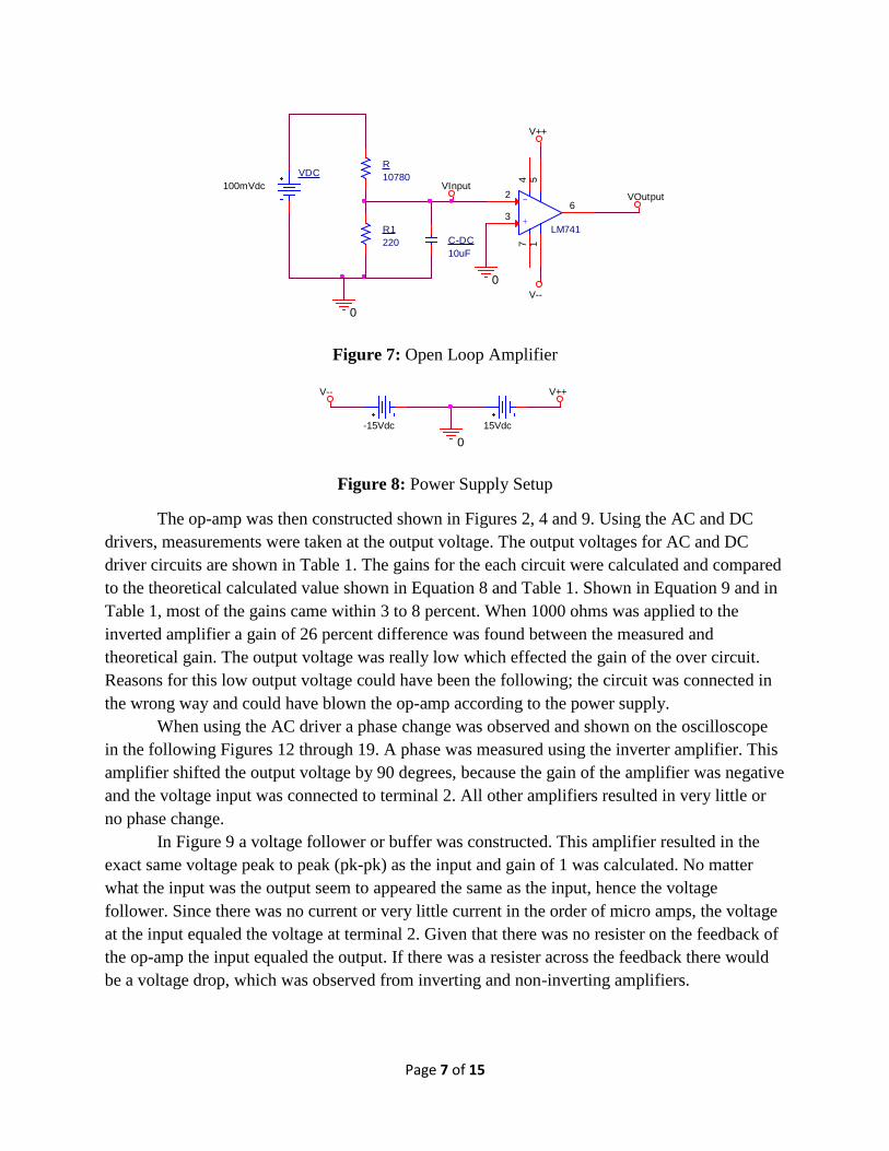
The LM741 op-amp was first constructed using an open loop amplifier shown in Figure
7. The positive voltage (V++) and negative voltage (V--) were connected to the power supply at
15 and -15 volts shown in Figure 8. Measurements were then taken with the input value at +
2mV and -2mV. The output voltage of the open loop amplifier was -13.5438 volts at +2mV input
and +14.3478 volts at -2mV input. The op-amp was concluded to be an inverting op-amp
because the input was connected to terminal 2 and the output voltage had an opposite sign from
the input. The gain and the stability of the amplifier were determined to have a gain of infinity or
a large number, because there was no feedback in the amplifier. The op-amp then saturated at the
power supply rails.
The output voltage can never be outside the range of the power supply. Due to the
internal components of the op-amp and there was no way an op-amp can create a higher voltage
than its supply. Inside an op-amp are many transistors that have a limit to how much a voltage
was applied. Notice that the output voltages were near the power rails. The integrated circuit of
an op-amp has many differential pair, current source transistors. Most op-amps have a common
emitter follower on the output stage. This allowed the op-amp to be close to the power rails
according to the saturation of the diode inside the transistor. To avoid hitting the rail voltage in a
open – loop circuit a gain of 10,000 was applied to the circuit. Using Equation 1 the input
voltage was accurately calculated to +1.3mV (highest input voltage) to -1.3mV (lowest input
voltage) to avoid the power rails, calculation shown in Equation 10. Of course at terminal 3 (V2
in equation) was set to 0, since it was connected to ground. The output voltage was set to 13
volts for the output to avoid the rails. This input voltage was low because the difference of the
two input voltage must be approximately 0 volts for the op-amp to be working correct.
R
220
R1
220
0
VAC
FREQ = 1KVAMPL = 100mVVOFF = 0
AC = 0
C-AC
.1uF
VInput
Page 7 of 15
Figure 7: Open Loop Amplifier
Figure 8: Power Supply Setup
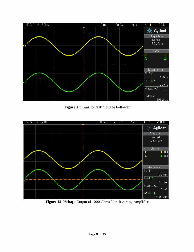
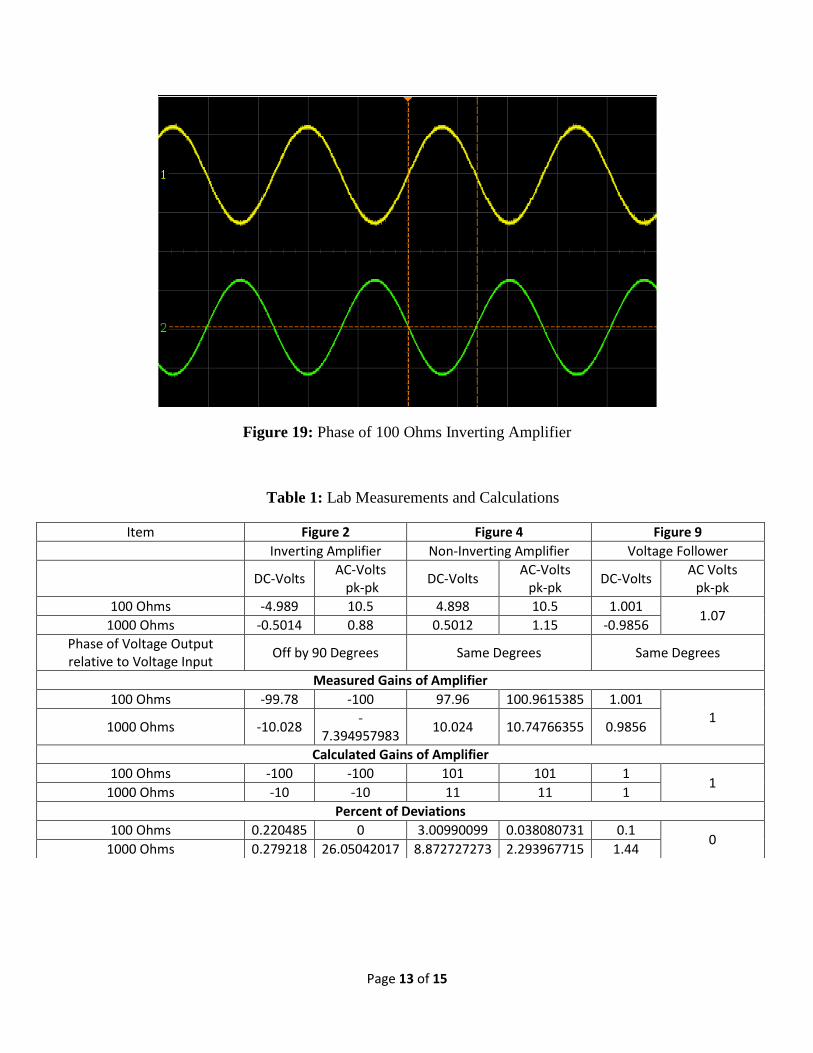
The op-amp was then constructed shown in Figures 2, 4 and 9. Using the AC and DC
drivers, measurements were taken at the output voltage. The output voltages for AC and DC
driver circuits are shown in Table 1. The gains for the each circuit were calculated and compared
to the theoretical calculated value shown in Equation 8 and Table 1. Shown in Equation 9 and in
Table 1, most of the gains came within 3 to 8 percent. When 1000 ohms was applied to the
inverted amplifier a gain of 26 percent difference was found between the measured and
theoretical gain. The output voltage was really low which effected the gain of the over circuit.
Reasons for this low output voltage could have been the following; the circuit was connected in
the wrong way and could have blown the op-amp according to the power supply.
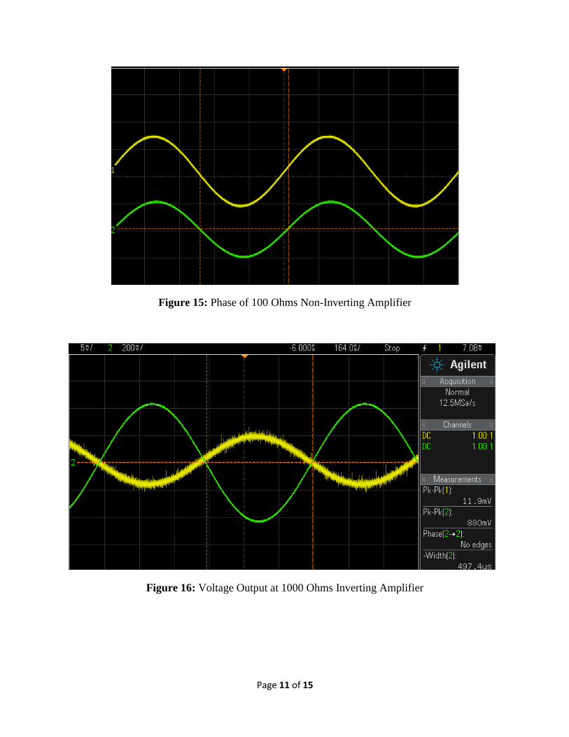
When using the AC driver a phase change was observed and shown on the oscilloscope
in the following Figures 12 through 19. A phase was measured using the inverter amplifier. This
amplifier shifted the output voltage by 90 degrees, because the gain of the amplifier was negative
and the voltage input was connected to terminal 2. All other amplifiers resulted in very little or
no phase change.
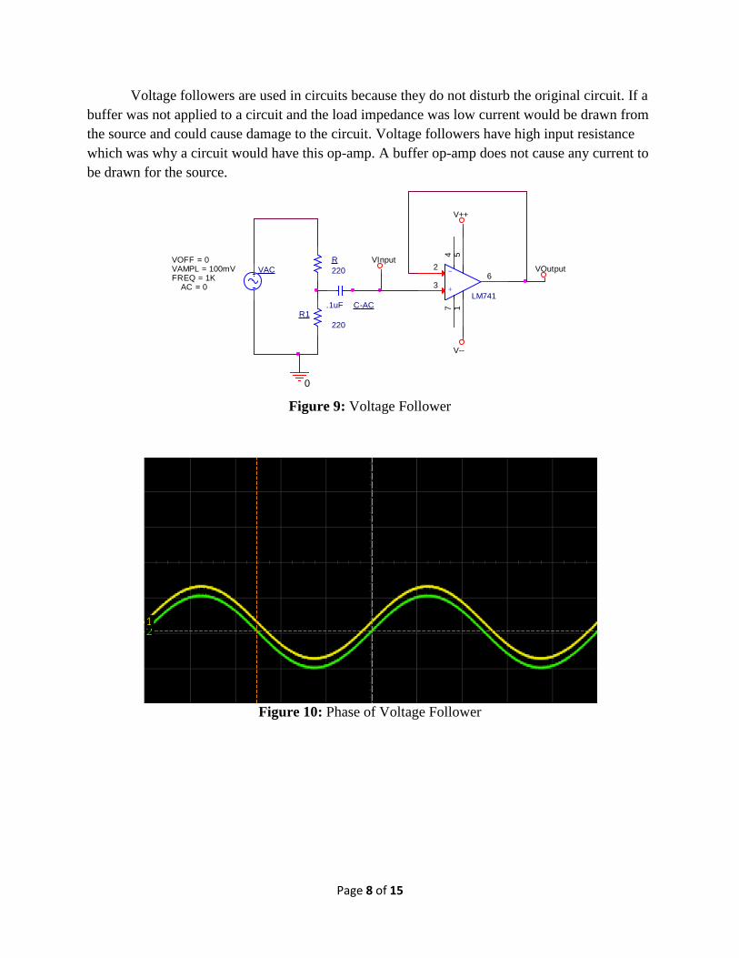
In Figure 9 a voltage follower or buffer was constructed. This amplifier resulted in the
exact same voltage peak to peak (pk-pk) as the input and gain of 1 was calculated. No matter
what the input was the output seem to appeared the same as the input, hence the voltage
follower. Since there was no current or very little current in the order of micro amps, the voltage
at the input equaled the voltage at terminal 2. Given that there was no resister on the feedback of
the op-amp the input equaled the output. If there was a resister across the feedback there would
be a voltage drop, which was observed from inverting and non-inverting amplifiers.
R
10780
R1
220
0
VInput
C-DC
10uF
VDC
100mVdc
-
+
LM741
3
26
7 14 5
0
VOutput
V++
V--
-15Vdc 15Vdc
V-- V++
0
Page 8 of 15
Voltage followers are used in circuits because they do not disturb the original circuit. If a
buffer was not applied to a circuit and the load impedance was low current would be drawn from
the source and could cause damage to the circuit. Voltage followers have high input resistance
which was why a circuit would have this op-amp. A buffer op-amp does not cause any current to
be drawn for the source.
Figure 9: Voltage Follower
Figure 10: Phase of Voltage Follower
R
220
R1
220
0
VInput
C-AC.1uF
-
+
LM741
3
26
7 14 5
VOutput
V++
V--
VACFREQ = 1KVAMPL = 100mVVOFF = 0
AC = 0
Page 9 of 15
Figure 11: Peak to Peak Voltage Follower
Figure 12: Voltage Output of 1000 Ohms Non-Inverting Amplifier
Page 10 of 15
Figure 13: Phase of 1000 Ohms Non- Inverting Amplifier
Figure 14: Voltage Output of 100 Ohms Non- Inverting Amplifier
Page 11 of 15
Figure 15: Phase of 100 Ohms Non-Inverting Amplifier
Figure 16: Voltage Output at 1000 Ohms Inverting Amplifier
Page 12 of 15
Figure 17: Phase of 1000 Ohms Inverting Amplifier
Figure 18: Voltage Output at 100 Ohms Inverting Amplifier
Page 13 of 15
Figure 19: Phase of 100 Ohms Inverting Amplifier
Item Figure 2 Figure 4 Figure 9
Inverting Amplifier Non-Inverting Amplifier Voltage Follower