Operational Amplifiers The operational amplifier (op-amp) was designed to perform mathematical operations. Although now superseded by the digital computer, op-amps are a common feature of modern analog electronics. The op-amp is constructed from several transistor stages, which commonly include a differential-input stage, an intermediate-gain stage and a push-pull output stage. The differential amplifier consists of a matched pair of bipolar transistors or FETs. The push-pull amplifier transmits a large current to the load and hence has a small output impedance. The op-amp is a linear amplifier with V out ∝ V in . The DC open-loop voltage gain of a typical op-amp is 10 2 to 10 6 . The gain is so large that most often feedback is used to obtain a specific transfer function and control the stability.
Transcript
Operational AmplifiersThe operational amplifier (op-amp) was designed to perform mathematical operations. Although now superseded by the digital computer, op-amps are a common feature of modern analog electronics.
The op-amp is constructed from several transistor stages, which commonly include a differential-input stage, an intermediate-gain stage and a push-pull output stage. The differential amplifier consists of a matched pair of bipolar transistors or FETs. The push-pull amplifier transmits a large current to the load and hence has a small output impedance.
The op-amp is a linear amplifier with
€
Vout ∝Vin . The DC open-loop voltage gain of a typical op-amp is 102 to 106 . The gain is so large that most often feedback is used to obtain a specific transfer function and control the stability.
Before proceeding we define a few terms:
linear amplifier- the output is directly proportional to the amplitude of input signal.open-loop gain, A- the voltage gain without feedback ( ≈105).closed-loop gain, G- the voltage gain with negative feedback (approximation to
€
H( jω) ).negative feedback- the output is connected to the inverting input forming a feedback loop (usually through a feedback resistor Rf ).
Cheap IC versions of operational amplifiers are readily available, making their use popular in any analog circuit. The cheap models operate from DC to about 20 kHz, while the high-performance models operate up to 50 MHz.
A popular device is the 741 op-amp which drops off 6 dB/octave above 5 Hz.
Op-amps are usually available as an IC in an 8-pin dual, in-line package (DIP). Some op-amp ICs have more than one op-amp on the same chip.
Figure 1a shows a complete diagram of an operational amplifier. A more common version of the diagram is shown in figure 1b, where missing parts are assumed to exist. The inverting input means that the output signal will be 180o out of phase with the input applied to this terminal. On the diagram +15V (DC) and -15V (DC). is typically, but not necessarily, +- 15V. The positive and negative voltages are necessary to allow the amplification of both positive and negative signals without special biasing.
Open-Loop Amplifiers
Figure.1: a) Complete diagram of an operational amplifier and b) common diagram of an operational amplifier.
+Vcc=+15V
-Vcc=-15V
For a linear amplifier (cf. a differential amplifier) the open-loop gain is
€
r v out = A( jω)(
r v i −
r v )
The open-loop gain can be approximated by the transfer function
where Ao is the DC open-loop gain and Hlow is the transfer function of a passive low-pass filter. We can write
€
A( jω) = AoHlow( jω)
€
A( jω) =Ao
1+ jω /ωowhere Ao~105 and fo~5 Hz
Two conditions must be satisfied for linear operation:
1. The input voltage must operate within the bias voltages:
2. For no clipping the output voltage swing must be restricted to
€
−Vcc ≤ vout ≤ +Vcc€
−Vcc / Ao ≤ (vi − v) ≤ +Vcc / Ao
Ideal Amplifier ApproximationThe following are properties of an ideal amplifier, which to a good approximation are obeyed by an operational amplifier:
1. large forward transfer function,2. virtually nonexistent reverse transfer function,3. large input impedance, Zin -> ∞ (any signal can be supplied to the op-amp
without loading problems),4. small output impedance, Zout ->0 (the power supplied by the op-amp is not
limited),5. wide bandwidth, and6. infinite gain, A ->∞ .
If these approximations are followed two rules can be used to analyze op-amp circuits:
Rule 1:The input currents Ii and I are zero, Ii= I= 0 (Zin =∞ ).Rule 2:The voltages Vi and V are equal, Vi= V (A =∞ ).
To apply these rules requires negative feedback.
Feedback is used to control and stabilize the amplifier gain. The open-loop gain is too large to be useful since noise will causes the circuit to clip. Stabilization is obtained by feeding the output back into the input (closed negative feedback loop). In this way the closed-loop gain does not depend on the amplifier characteristics.
Non-inverting AmplifiersFigure .2 shows a non-inverting amplifier, sometimes referred to as a voltage follower.
Figure 2: Non-inverting, unity-gain amplifier.
Applying our rules to this circuit we have
€
Vi = V ⇒Vin = Vout
Ii = I = 0 ⇒ Rin = ∞
The amplifier gives a unit closed-loop gain,
€
G( jω) =1 , and does not change the sign of the input signal (no phase change).This configuration is often used to buffer the input to an amplifier since the input resistance is high, there is unit gain and no inversion. The buffer amplifier is also used to isolate a signal source from a load.
Often a feedback resistor is used as shown in figure .3.
Figure 3: Non-inverting amplifier with feedback.
For this circuit
The gain is
with
€
Vi = V ⇒Vin =RI
RI + Rf
Vout
€
Vout
Vin
=Ri + RI
RI
=1+RF
RI
G( jω) =1+RF
RI
Inverting Amplifiers
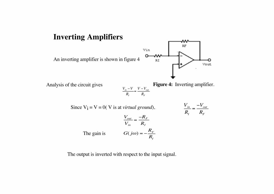
An inverting amplifier is shown in figure 4
Analysis of the circuit gives
€
Vin −VRI
=V −Vout
RF
Since Vi = V = 0( V is at virtual ground),
€
Vin
RI
=−Vout
RF
The gain is
€
Vout
Vin
=−RF
RI
G( jω) = −RF
RI
The output is inverted with respect to the input signal.
Figure 4: Inverting amplifier.
The input impedance of the inverting amplifier is Rin=Vin/I. Since Vin=IRI we have .Rin=RIA better circuit for approximating an ideal inverting amplifier is shown in figure
Inverting amplifier with bias compensation.
The extra resistor is a current bias-compensation resistor. It reduces the current bias by eliminating non-zero current at the inputs.
A sketch of the frequency response of the inverting and non-inverting amplifiers are shown in figure
Mathematical OperationsCurrent Summing AmplifierConsider the current-to-voltage converter shown in figure. Applying our ideal amplifier rules gives
€
Vi = V = 0 ⇒ 0 −Vout = iRF
Therefore Vout=-iRF and the circuit acts as a current-to-voltage converter.
Figure shows several current sources driving the negative input of an inverting amplifier.
Summing the current into the node givesCurrent summing amplifier.
€
V1
R1
+V2
R2
+V3
R3
= −Vout
RF
If
€
R1 = R2 = R3 ≡ R
€
Vout = −RF
R(V1 + V2 + V3)the output voltage is proportional to the
sum of the input voltages.
For only one input and a constant reference voltage
€
Vout = −RF
RI
Vin −RF
RR
Vref
where the second term represents an offset voltage. This provides a convenient method for obtaining an output signal with any required voltage offset.
Differentiation Circuit
To obtain a differentiation circuit we replace the input resistor of the inverting amplifier with a capacitor as shown in figure
Replacing RI with Zc = 1/(jω C)in the voltage
gain gives
€
Vout = G( jω)Vin = −RZc
Vin = − jωRCVin = −RC dVin
dt
The frequency response is shown in figure
Integration Circuit
Integration is obtained by reversing the resistor and the capacitor as shown in figure . The capacitor is now in the feedback loop.
Analysis gives
We can combine the above inverting, summing, offset, differentiation and integration circuits to build an analog computer that can solve differential equations. However, today, the differentiators and integrators are mainly used to condition signals.
€
G( jω) =Vout
Vin
= −Zc
R=
−1jωRC
⇒Vout =−1RC
Vindt∫
The frequency response is shown in figure
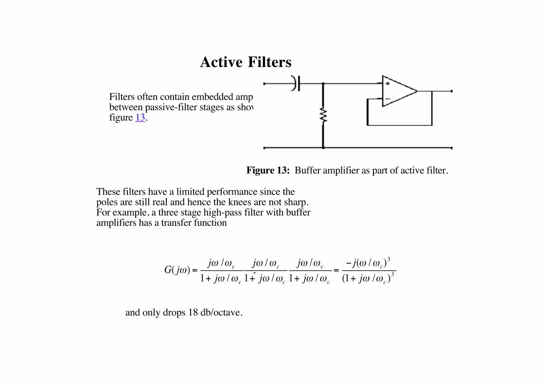
Active Filters
Filters often contain embedded amplifiers between passive-filter stages as shown in figure 13.
Figure 13: Buffer amplifier as part of active filter.
These filters have a limited performance since the poles are still real and hence the knees are not sharp. For example, a three stage high-pass filter with buffer amplifiers has a transfer function
€
G( jω) =jω /ω c
1+ jω /ω c
jω /ω c
1+ jω /ωc
jω /ω c
1+ jω /ω c
=− j(ω /ω c)3
(1+ jω /ω c )3
and only drops 18 db/octave.
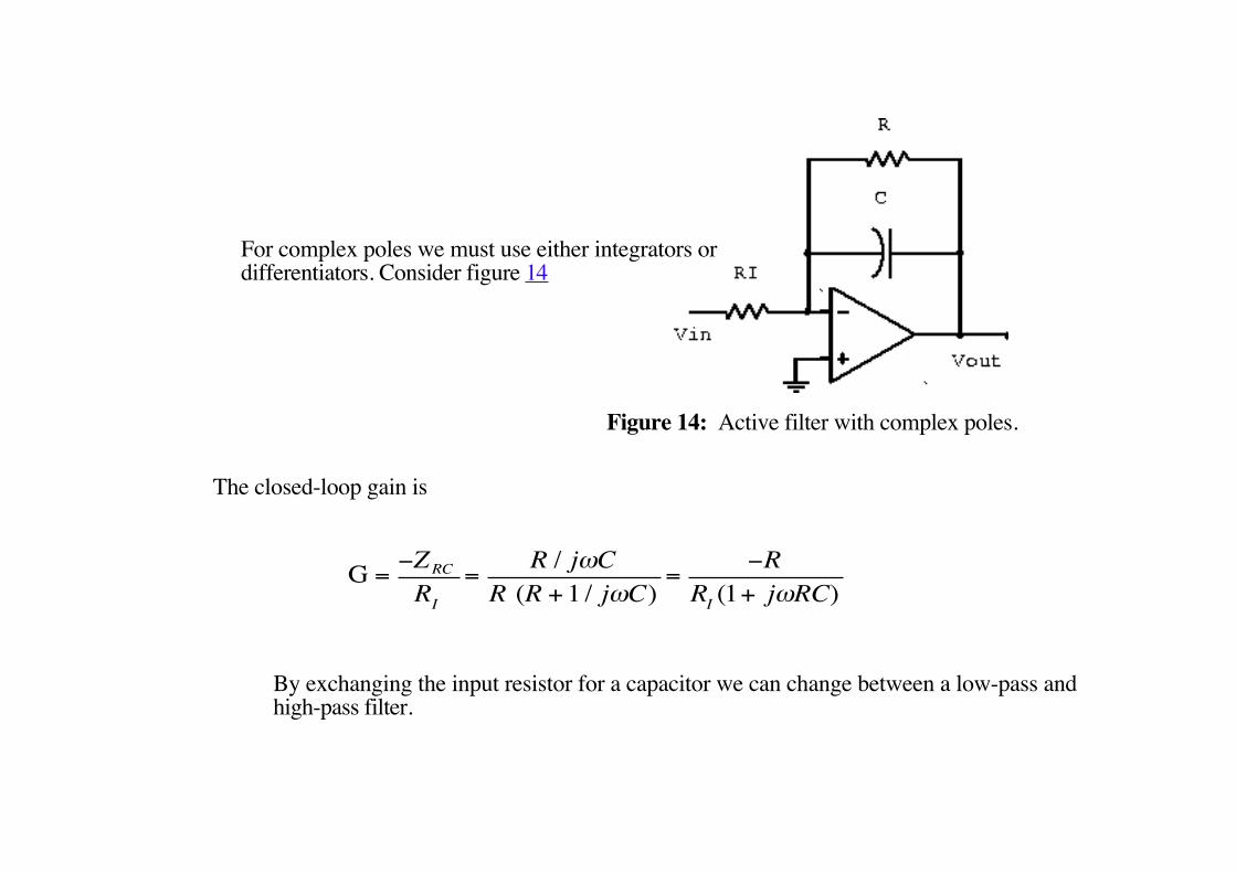
For complex poles we must use either integrators or differentiators. Consider figure 14
Figure 14: Active filter with complex poles.
The closed-loop gain is
€
G =−ZRC
RI
=R / jωC
R (R + 1 / jωC)=
−RRI (1+ jωRC)
By exchanging the input resistor for a capacitor we can change between a low-pass and high-pass filter.
General Feedback ElementsThe feedback elements in an operation amplifier design can be more complicated than a simple resistor and capacitor. An interesting feedback element is the analog multiplier as defined in figure 15.
Figure 15: Five-terminal network that performs the multiplication operation on two voltage signals.
The multiplier circuit itself can be thought of as another op-amp with a feedback resistor whose value is determined by a second input voltage. Multiplication circuits with the ability to handle input voltages of either sign (four-quadrant multipliers) are available as integrated circuits and have a number of direct uses as multipliers. But when used in a feedback loop around an operational amplifier, other useful functional forms result.
The circuit of figure 16 gives an output that is the ratio of two signals, whereas the circuit of figure 17 yields the analog square-root of the input voltages.
Figure 16: A multiplier as part of the feedback loop that results in the division operation.
Figure 17: A multiplier as part of the feedback loop that results in the square-root operation.
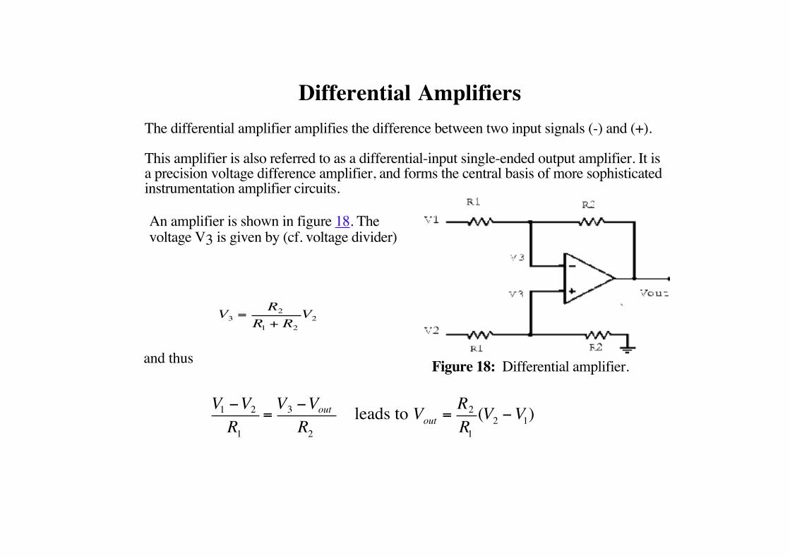
Differential AmplifiersThe differential amplifier amplifies the difference between two input signals (-) and (+).
This amplifier is also referred to as a differential-input single-ended output amplifier. It is a precision voltage difference amplifier, and forms the central basis of more sophisticated instrumentation amplifier circuits.
An amplifier is shown in figure 18. The voltage V3 is given by (cf. voltage divider)
Figure 18: Differential amplifier.€
V3 =R2
R1 + R2
V2
€
V1 −V2
R1
=V3 −Vout
R2
leads to Vout =R2
R1
(V2 −V1)
and thus
Analysis Using Finite Open-Loop Gain
The infinite gain approximation is very useful but a more complete description is required if we are to understand the limitations of the op-amp.
Real op-amps have a large but finite input impedance, small but non-zero output impedance and large but finite open-loop gain.
They also have voltage and current asymmetries at the inputs. We will analyze some circuits using an finite open-loop gain and consider output impedance, input impedance, and voltage and current offsets.
An op-amp will in general have a small resistive output impedance from the push-pull output stage. We will model the open-loop output impedance by adding a series resistor to the output of an ideal op-amp as shown in figure .
Output Impedance
Real, current-limiting operational amplifier partially modeled by an ideal amplifier and an output resistor.
Assuming no current into the input terminals (unloaded), and hence no current through Ro , we have V1=Vout=V(open) . Using the open-loop transfer function V1=A(jω)(Vin-Vout) we obtain
€
V (open) =A( jω)
1+ A( jω)Vin
Shorting a wire across the output gives Vout=0 and hence
€
I(short) =V1
R0
=A( jω)
R0
Vin
Using the standard definition for the impedance gives
€
Zout =V (open)I(short)
=R0
1+ A( jω)
If A~Ao>>1 than Zout ~Ro/Ao, which is small as required by our infinite open-loop gain approximation
We can now draw the impedance outside the feedback loop and use
€
A( jω ) =A0
1+ jω /ωc
=A0
1+r s /ωc
to obtain
€
Zout =R0ωc + R0
r s
ωc (1+ A0) +r s
The circuit can now be modeled by a resistor Ro/Ao in series with an inductorRo/(Ao ω) all in parallel with another resistor Ro (three passive components) as shown in figure
An equivalent circuit for a 741-type operational amplifier.
If the op-amp is used to drive a capacitive load, the inductive component in the output impedance could set up an LCR resonant circuuit which would result in a slight peaking of the transfer function near the corner frequency as shown in figure
Input ImpedanceWhen calculating the output impedance we still assumed an infinite input impedance. In this section we will calculate the finite input impedance assuming a zero output impedance. We consider a model that assumes an internal resistor connecting the inverting and non-inverting input terminals of the op-amp as shown in figure 31Consider an inverting amplifier and remove the input resistor so that the input impedance can be calculated directly at the amplifier's input terminals.
Fig.31 Model for calculating the input impedance of the inverting amplifier.
€
Zin =V1
I1
The input impedance is defined by
and the current at the summing junction is
€
I1 =V1
RT1
+ I2
The current through the feedback resistor is
and the output voltage is related to by the open-loop gain
€
Vout = A( jω)(0 −V1)
€
I2 =V −Vout1
RF
The resulting input impedance is thus
€
Zin =RT RF
RF + RT (1+ A( jω))
For large A
€
Zin =RF
A( jω)
The closed-loop input impedance is thus small and almost independent of the large RF of the operational amplifier.
Now consider the non-inverting amplifier shown in figure 32
Fig.32 Model for calculating the input impedance of the non-inverting amplifier.
Now calculate the input impedance by recognizing that I1 is much less than I2 , since RT is much greater than R1 or R2
€
Zin = RTA( jω) + G( jω)
G( jω)where G(jω) is the closed-loop gain of the amplifier. Notice that in contrast to the low input impedance for the inverting amplifier, the non-inverting amplifier exhibits a closed-loop input impedance that is much larger than the open-loop value RT .
Voltage and Current OffsetsSince op-amps are generally DC coupled, there will appear a nonzero output even when the inputs are grounded or connected to give no input signal. The voltage offset is the result of slightly different transistors making up the differential input stage. The voltage offset can be reduced by using an externally-adjustable bias resistor (voltage offset null circuitry).
The current offsets at the inverting and non-inverting input terminals are usually base currents into two identical bipolar transistors. Thus their difference can be expected to be much less than either base current alone. Using this fact the student should be able to explain the reason for having an extra resistor between the non-inverting input and ground for the inverting amplifier. The resistor should have a value equal to the input resistor and feedback resistor in parallel.
We define the following:
output offset voltage - The voltage at the output when the input voltage is zero (input terminals grounded).
common mode voltage - The voltage at the output when the voltage at the inverting and non-inverting inputs are equal.
common mode rejection ratio (CMRR) - The ratio of the op-amp gain when operating in differential mode to the gain when operating in common mode.
common mode rejection (CMR) - The ability to respond to only differences at the input terminals: .
Current Limiting and Slew RateThe presence of resistance at the output of the op-amp limits the current that the amplifier can deliver into a load, as shown in figure 33. Current limiting is a nonlinear property that invalidates the two normal approximation rules. When an op-amp is driven into a current-limiting condition it goes into saturation and becomes a constant current source. For a large load the output signal will be voltage-limited. A similar breakdown of the rules occurs when the amplifier is driven into voltage-limited operation.
Figure 33: a) Voltage-limited and current-limited operational regions for an operational amplifier and b) definition of slew rate and settling time for an operational amplifier.
The op-amp performance can be demonstrated by applying a step function to the input and observing the output response, as shown in figure 33b. The actual output will have a finite slope (slew rate) and overshoot the final voltage value. It then approaches the final voltage either exponentially or with some damped ringing.
The slew rate and overshoot are nonlinear effects. The settling time after amplifier saturation is defined as the time between the edge of the applied step function and the point where the amplifier output settles to within some stated percentage of the target voltage value.
Problems1 Consider the circuit below. (You may assume that the op-amps are ideal.)
1. Write an expression for the transfer function . Express your result in terms of the amplitude of the output and the phase relative to the input. Let k , , F and F. Do not simplify the algebra.
2. What are the (real) zeroes in the transfer function, if any?3. What are the (real) poles in the transfer function if any?4. Sketch the transfer function as a function of on a log-log plot. Your sketch
should show the slope of in the large and small limits, the corner frequencies, and the value of at the corner frequencies.
5. Describe the dependence of the output on frequency at small and large frequencies in dB/octave.
Problem 2.
1. Write the two rules for the analysis of circuits which utilize ``ideal'' op-amps.2. Write an expression for the potential for the following circuit.
5. Let Z1=1kOhm and Z2= 10k . Sketch a log-log plot showing the function for the above circuit assuming that a general purpose op-amp such as the 741 is used.
6. The 741 op-amp has a corner frequencies of 4 Hz, DC open-loop gain of 2x10**5 and a fall off at high frequency of 6 dB/octave. What is the frequency domain over which the amplifier defined in part (c) will have constant gain? What is the gain of the amplifier in this frequency domain?
7. Suppose now that the impedance Z1 is replaced with a capacitor with a capacitance C . For frequencies much greater than 4 Hz, the 741 op-amp will attenuate the signal if the product RC is greater than some maximum value. For a frequency of 50 kHz, what is the maximum value for C for which the op-amp
€
A (ω) will not attenuate the output signal at high frequencies?
Hint: If you sketch and , you will be able to see the constraint on .
Problem 3. Set up an operational amplifier circuit to solve the equation
€
d2 xdt2 + 5 dx
dt+ 7x + 3= 0
Hint: the input is .
€
d2xdt2
Problem 4. Draw a schematic diagram of a circuit for which
€
Vout = ln(Vin ) . Specify the limitations on the input voltage range, if any.