116
OPTI510R: Photonics Khanh Kieu College of Optical Sciences, University of Arizona [email protected] Meinel building R.626

OPTI510R: Photonics
Khanh Kieu
College of Optical Sciences,
University of Arizona
Meinel building R.626

Announcement
Homework #6 is due today
Final exam May 2, room 307, starting at 11 AM
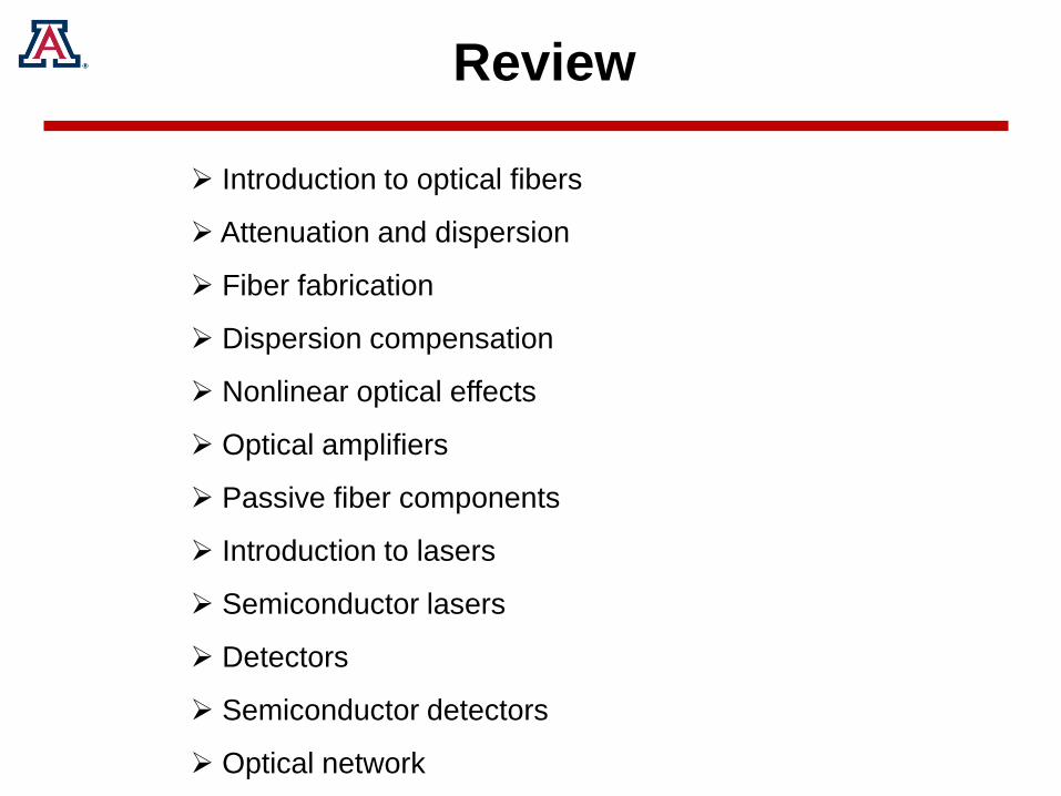
Review
Introduction to optical fibers
Attenuation and dispersion
Fiber fabrication
Dispersion compensation
Nonlinear optical effects
Optical amplifiers
Passive fiber components
Introduction to lasers
Semiconductor lasers
Detectors
Semiconductor detectors
Optical network

Goals
Understand the most important concepts in
Photonics
Learn the working principles of photonics
devices
Identify the remaining challenges in the field
Think about possible solutions

Introduction to optical fibers

Optical fibers
The working principle of standard optical
fiber can be explained using TIR
Standard fiber PCF HC-PCF
Photonics crystal fibers
J. C. Knight, “Photonic crystal fibers,” Nature 424, 847-851 (2003)
The refractive index of the
core is smaller than the
refractive index of the cladding
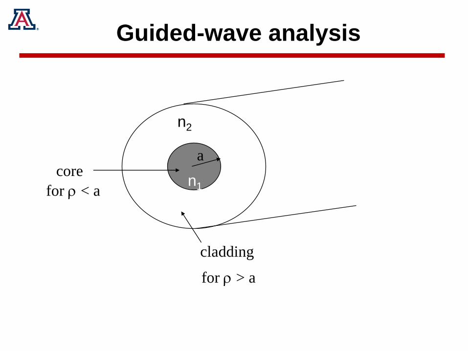
Guided-wave analysis
acore
cladding
for < a
for > a
n1
n2

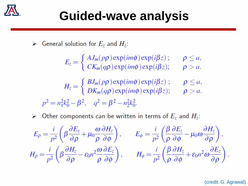
Guided-wave analysis
(credit: G. Agrawal)

Guided-wave analysis
(credit: G. Agrawal)
Guided-wave analysis
(credit: G. Agrawal)
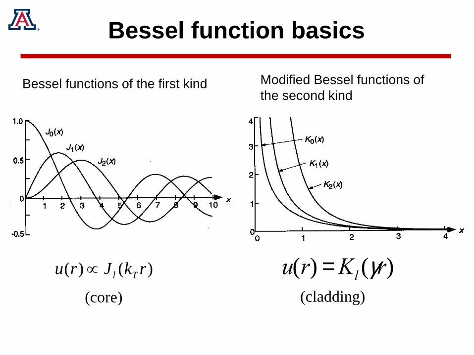
Bessel function basics
)()( rkJru Tl
u(r) =Kl (gr)
(core) (cladding)
Bessel functions of the first kind Modified Bessel functions of
the second kind
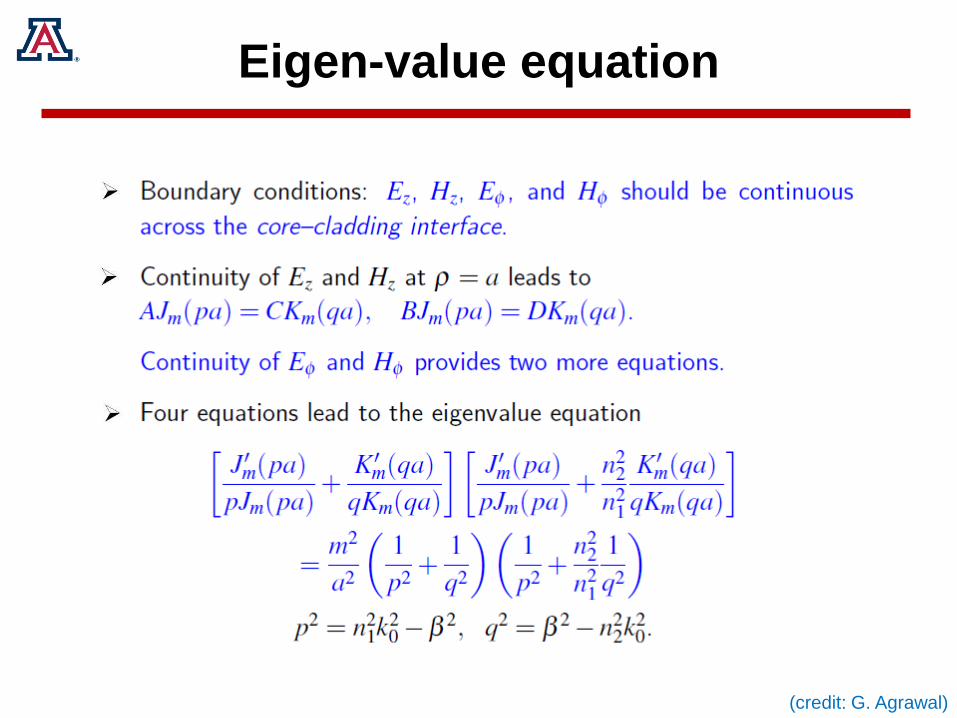
Eigen-value equation
(credit: G. Agrawal)
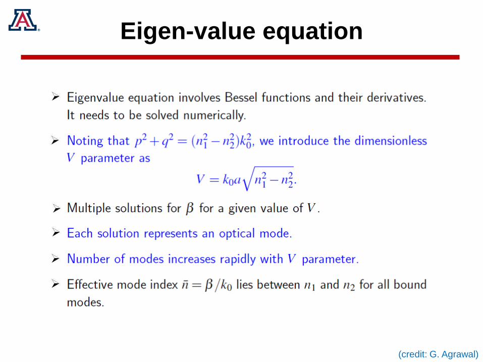
Eigen-value equation
(credit: G. Agrawal)

Eigen-value equation
(credit: G. Agrawal)
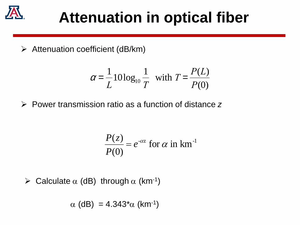
Attenuation in optical fiber
Attenuation coefficient (dB/km)
Power transmission ratio as a function of distance z
a =1
L10log10
1
T with T =
P(L)
P(0)
1-z- kmin for )0(
)(e
P
zP
Calculate (dB) through (km-1)
(dB) = 4.343* (km-1)

Sources of attenuation in silica fiber
Absorption
• Vibrational transitions in the IR
• Electronic and molecular transitions in the UV
• Extrinsic absorption from adsorbed water and other impurities
Scattering
• Rayleigh scattering
• Extrinsic scattering from defects due to manufacturing errors
• Raman, Brillouin scattering

Propagation loss in optical fiber
Current loss is < 0.2dB/km for single mode fiberworking around 1550nm
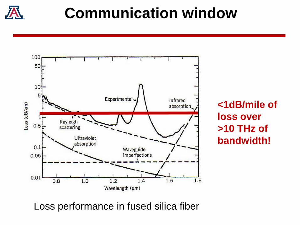
Communication window
Loss performance in fused silica fiber
<1dB/mile of
loss over
>10 THz of
bandwidth!

Dispersion in optical fiber
Modal dispersion• Occurs in multimode fibers coming from differences in group velocity for
different modes
Material dispersion• Results from the wavelength dependence of the bulk refractive index
Waveguide dispersion• Results from the wavelength dependence of the effective index in a
waveguide
• Material + waveguide dispersion is termed chromatic dispersion
Polarization mode dispersion• Results from the fact that different polarizations travel at different speeds
due to small birefringence that is present
Nonlinear dispersion – example is self-phase modulation

Modal dispersion
Modal dispersion occurs in multimode fibers as a result of differences in
the group velocities of the various modes.
A single pulse of light entering an M-mode fiber spreads into M pulses.
Estimate of pulse spread
– Where vmin and vmax are the smallest and largest group velocity of the modes.
For step index fiber,
,2
1
maxmin
v
L
v
L
2
1
2
2
2
11max1min 2/)(,),1( nnncvcv
12c
L
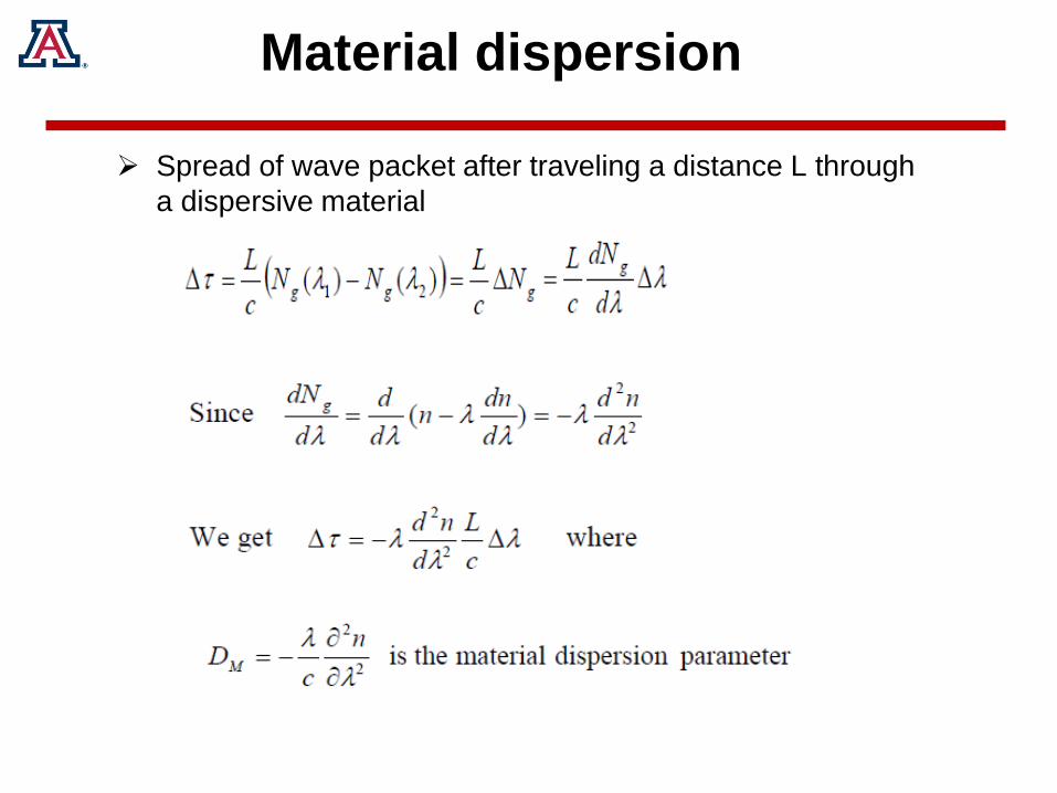
Spread of wave packet after traveling a distance L through
a dispersive material
Material dispersion
Waveguide dispersion

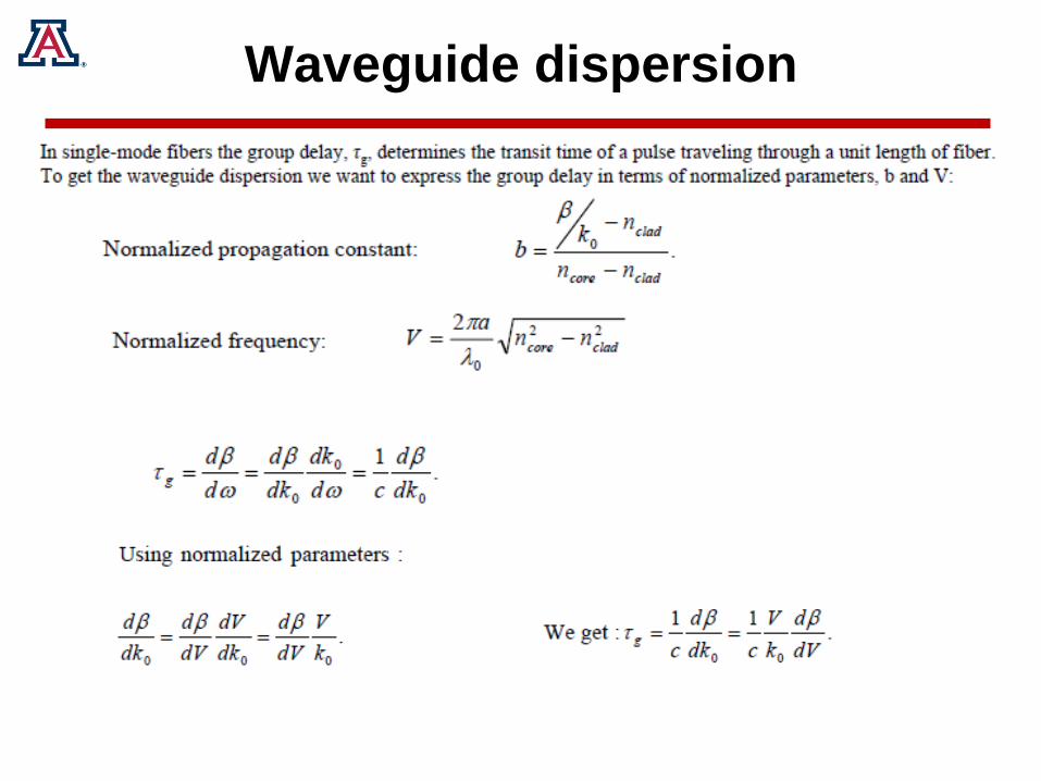
Waveguide dispersion
m : material delay
w : waveguide delay
Waveguide dispersion!

Waveguide dispersion
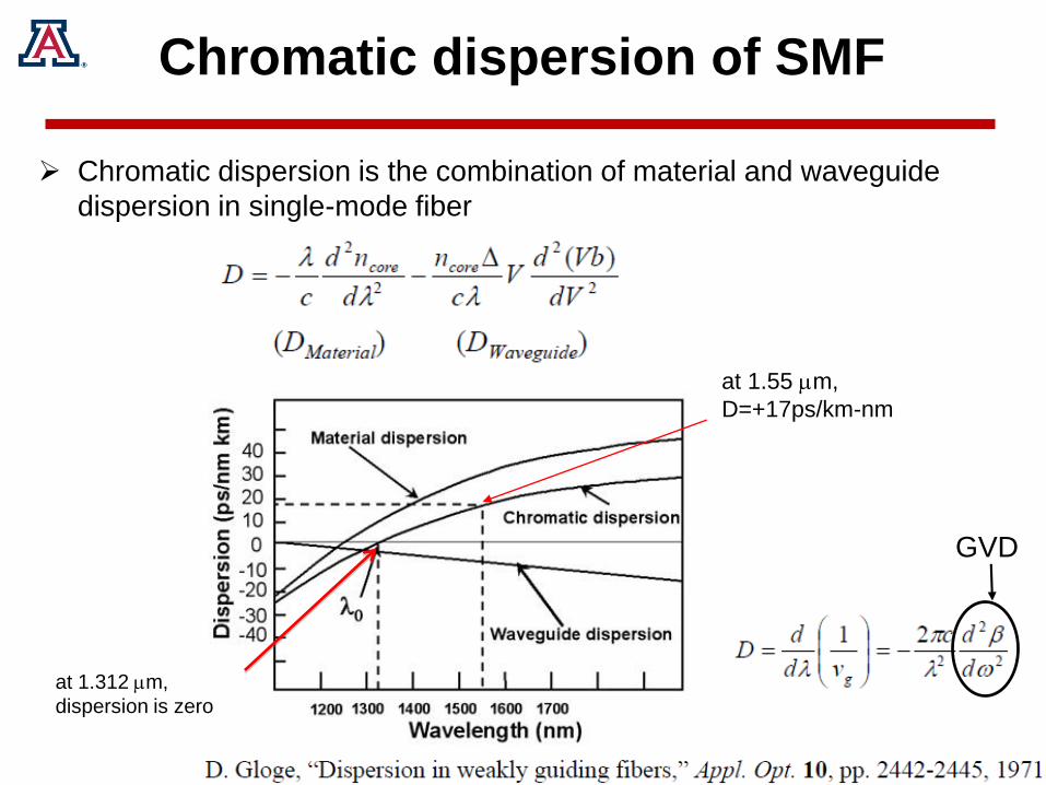
Chromatic dispersion of SMF
Chromatic dispersion is the combination of material and waveguide
dispersion in single-mode fiber
at 1.312 mm,
dispersion is zero
at 1.55 mm,
D=+17ps/km-nm
GVD
Fabrication techniques
• Fiber preform fabrication
• Fiber pulling

Rod-in-tube technique
Rod-in-tube method: UA
UA fiber drawing towerHigh precision ultrasonic drilling and grinding
machines for glass rod processing
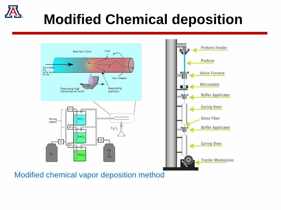
Modified Chemical deposition
Modified chemical vapor deposition method

Active fiber fabrication
Nano-particle vapor deposition (Liekki)MCVD process
http://www.youtube.com/watch?v=6CqT4DuAVxs
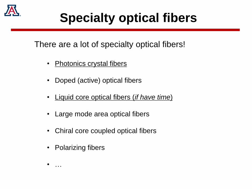
Specialty optical fibers
There are a lot of specialty optical fibers!
• Photonics crystal fibers
• Doped (active) optical fibers
• Liquid core optical fibers (if have time)
• Large mode area optical fibers
• Chiral core coupled optical fibers
• Polarizing fibers
• …

Photonics crystal fibers
a PCF preform
J. C. Knight, “Photonic crystal fibers,” Nature 424, 847-851 (2003)
Standard fiber PCF HC-PCF
Dispersion compensation
Dispersion compensation
• Pre-chirp technique
• Dispersion compensating fibers
• Chirped fiber Bragg grating

Dispersion compensating fibers
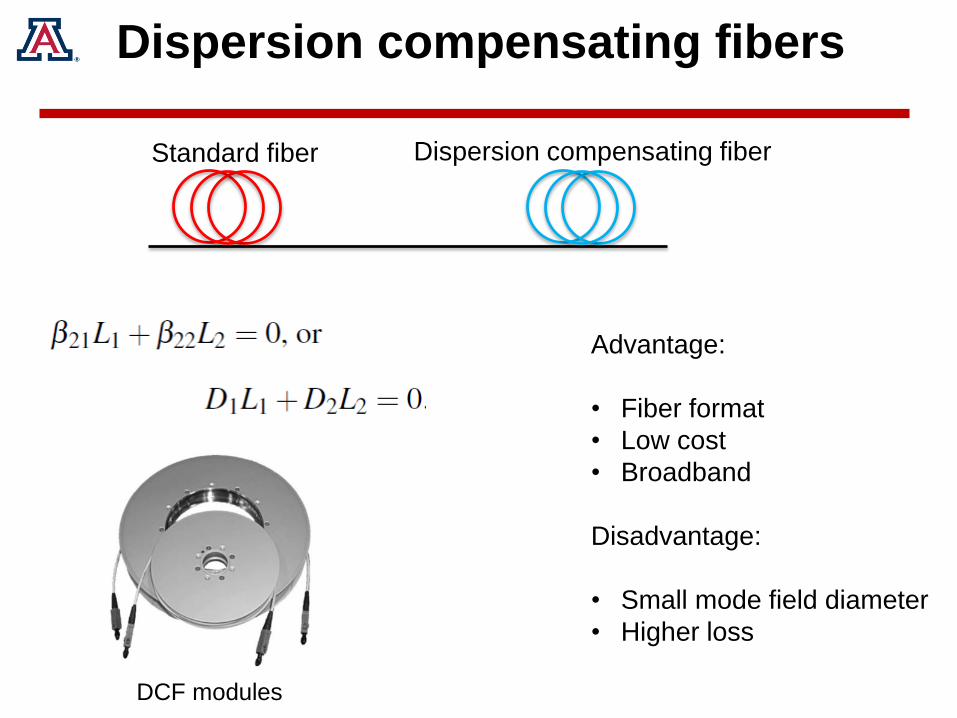
Dispersion compensating fibers
Standard fiber Dispersion compensating fiber
Advantage:
• Fiber format
• Low cost
• Broadband
Disadvantage:
• Small mode field diameter
• Higher loss
DCF modules
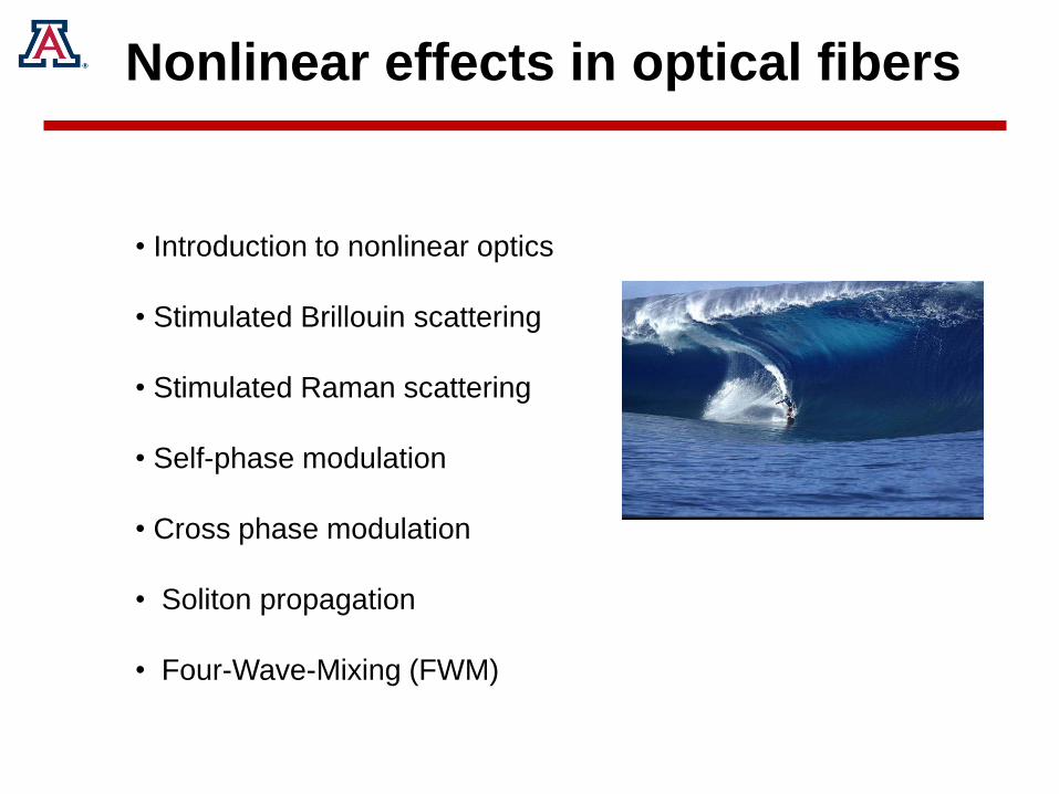
Nonlinear effects in optical fibers
• Introduction to nonlinear optics
• Stimulated Brillouin scattering
• Stimulated Raman scattering
• Self-phase modulation
• Cross phase modulation
• Soliton propagation
• Four-Wave-Mixing (FWM)

Nonlinear optics
E
Electron
(2), (3)… are very small
R. W. Boyd, Nonlinear Optics, (Academic Press, 2008)

Nonlinear optical effects
• Second harmonic generation (SHG)
• Third harmonic generation (THG)
• High harmonic generation (HHG)
• Sum/Difference frequency generation (SFG/DFG)
• Optical parametric processes (OPA, OPO, OPG)
• Kerr effect
• Self-focusing
• Self-phase modulation (SPM)
• Cross-phase modulation (XPM)
• Four-wave mixing (FWM)
• Multiphoton absorption
• Photo-ionization
• Raman/Brillouin scattering
• and more…

Stimulated Brillouin scattering
• Predicted by Leon Brillouin in 1922
• Scattering of light from acoustic waves
• Becomes a stimulated process when input power exceeds a
threshold level
• Low threshold power for long fibers (5 mW)
Most of the power reflected
backward after SBS threshold
is reached!

Stimulated Brillouin scattering
• Pump produces density variations through
electrostriction, resulting in an index grating which
generates Stokes wave through Bragg diffraction
• Energy and momentum conservation require:
B = p - s; kA =kp – ks
• Acoustic waves satisfy the dispersion relation:
B = vA*|kA| = vA*|(kp – ks)| 2* vA*|kp| = 2* vA*2*np/ p
fA = B/2 = 2* vA*2*np/ p ~ 11GHz
if we use A = 5.96 km/s, np = 1.45, and p =
1550nm
SBS
(Brillouin frequency shift)

Brillouin gain spectrum in optical
fibers
• Measured spectra for (a) silica-core (b) depressed-cladding, and
(c) dispersion-shifted fibers
• Brillouin gain spectrum is quite narrow (50 MHz)
• Brillouin shift depends on GeO2 doping within the core
• Multiple peaks are due to the excitation of different acoustic modes
G. P. Agrawal, Nonlinear Fiber Optics, (Academic Press, 2007)

Brillouin threshold in optical fibers
is the fiber loss
gB is the Brillouin gain coefficient
Le is the effective length
Pth is the Brillouin threshold
G. P. Agrawal, Nonlinear Fiber Optics, (Academic Press, 2007)

Stimulated Raman scattering
• Discovered by C. V. Raman in 1928
• Scattering of light from vibrating silica molecules
• Amorphous nature of silica turns vibrational state into a band
• Raman gain is maximum near 13 THz
• Scattered light red-shifted by 100 nm in the 1.5 mm region
G. P. Agrawal, Nonlinear Fiber Optics, (Academic Press, 2007)
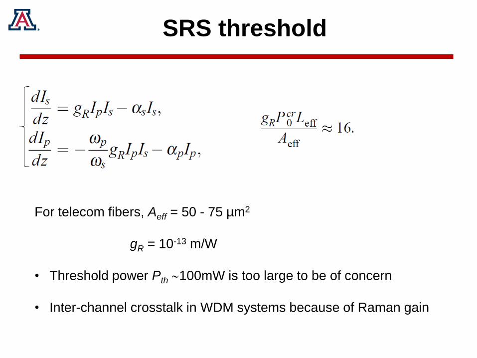
SRS threshold
For telecom fibers, Aeff = 50 - 75 µm2
gR = 10-13 m/W
• Threshold power Pth 100mW is too large to be of concern
• Inter-channel crosstalk in WDM systems because of Raman gain

Self-phase modulation (SPM)
First observed inside optical fiber by
Stolen and Lin (1978)
90-ps pulses transmitted
through a 100-m-long fiber
Output spectrum depends on shape and chirp of input pulses.
Even spectral compression can occur for suitably chirped pulses
NL = .P0.L
Output spectrum
as the function of
the nonlinear phase
shift

Optical Amplifiers
Erbium Doped Fiber Amplifiers (EDFAs)
Semiconductor Optical Amplifiers
Raman Amplifiers
Optical Parametric Amplifiers

Types of Optical Amplifiers
Erbium Doped Fiber Amplifiers (EDFA’s)
• Best performance
• Low cost, robust
• Wide spread use
Semiconductor Optical Amplifiers
• Small package
• Potential use for low-cost
applications
• Potential use for optical switching
Raman Amplifiers
• Better noise performance compared
to EDFA
Optical parametric amplifier
• High gain, broader bandwidth
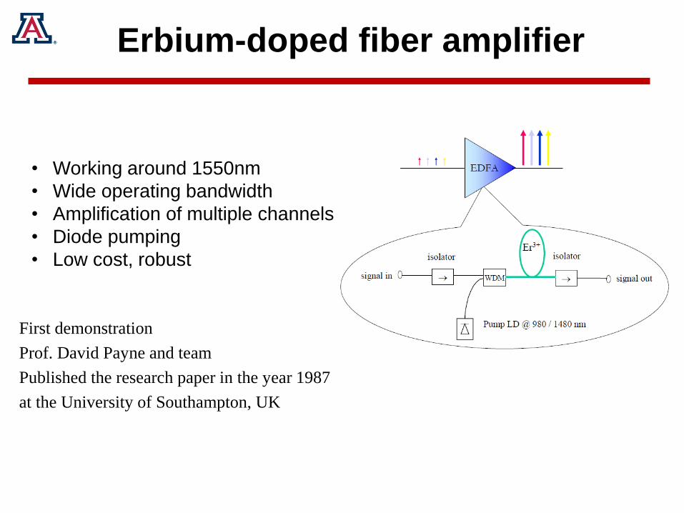
Erbium-doped fiber amplifier
• Working around 1550nm
• Wide operating bandwidth
• Amplification of multiple channels
• Diode pumping
• Low cost, robust
First demonstration
Prof. David Payne and team
Published the research paper in the year 1987
at the University of Southampton, UK

Erbium-doped fiber amplifier
Main pump wavelengths: 980nm and 1480nm
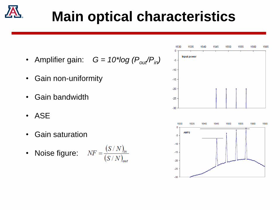
Main optical characteristics
• Amplifier gain: G = 10*log (Pout/Pin)
• Gain non-uniformity
• Gain bandwidth
• ASE
• Gain saturation
• Noise figure:
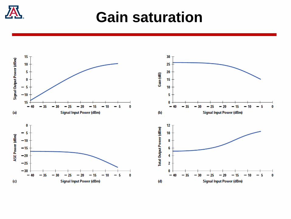
Gain saturation

Typical amplifier performance

EDFA: Disadvantages
• Can only work at a narrow wavelength range (C and L band)
• Requires specially doped fiber as gain medium
• Three-level system, so gain medium is opaque at signal wavelengths until pumped
• Requires long path length of gain medium (tens of meters in glass)
• Gain very wavelength-dependent and must be flattened
• Gain limited by cooperative quenching
• Relatively high noise figure due to ASE
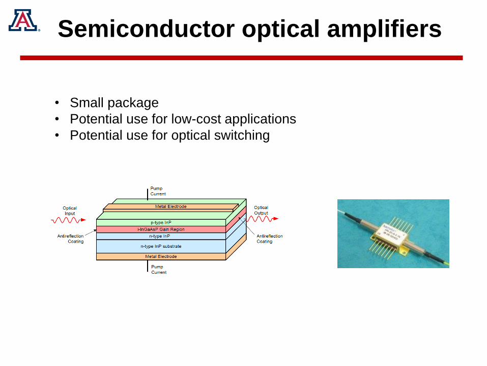
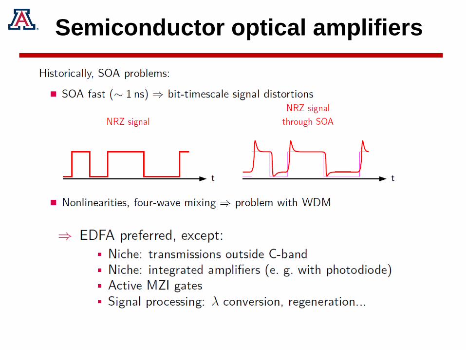
Semiconductor optical amplifiers
• Small package
• Potential use for low-cost applications
• Potential use for optical switching

Semiconductor optical amplifiers
Performance of a typical SOA
Compared to EDFA: Lower gain, high noise figure, and lower output power
Semiconductor optical amplifiers
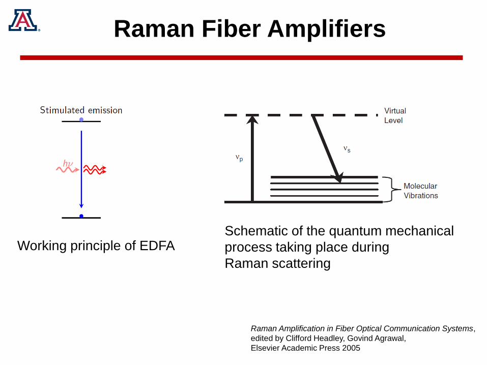
Raman Fiber Amplifiers
Working principle of EDFASchematic of the quantum mechanical
process taking place during
Raman scattering
Raman Amplification in Fiber Optical Communication Systems,
edited by Clifford Headley, Govind Agrawal,
Elsevier Academic Press 2005

Raman Fiber Amplifiers
Raman gain profiles for a 1510-nm pump in three different fiber types.
SMF, standard single mode fiber; DSF, dispersion shifted fiber; DCF, dispersion
compensating fiber

Raman Fiber Amplifiers
Schematic diagram of a Raman amplifier

Raman Fiber Amplifiers
Evolution of signal power in a bidirectionally pumped, 100-km-long
Raman amplifier as the contribution of forward pumping is varied from 0 to 100%
Which one is better? Co-pumping or Counter-pumping?

Optical Parametric Amplifier
Degenerate and non-degenerate FWM process depicted on an energy level diagram
Require optical fiber with zero dispersion near the pump wavelength for phase
matching
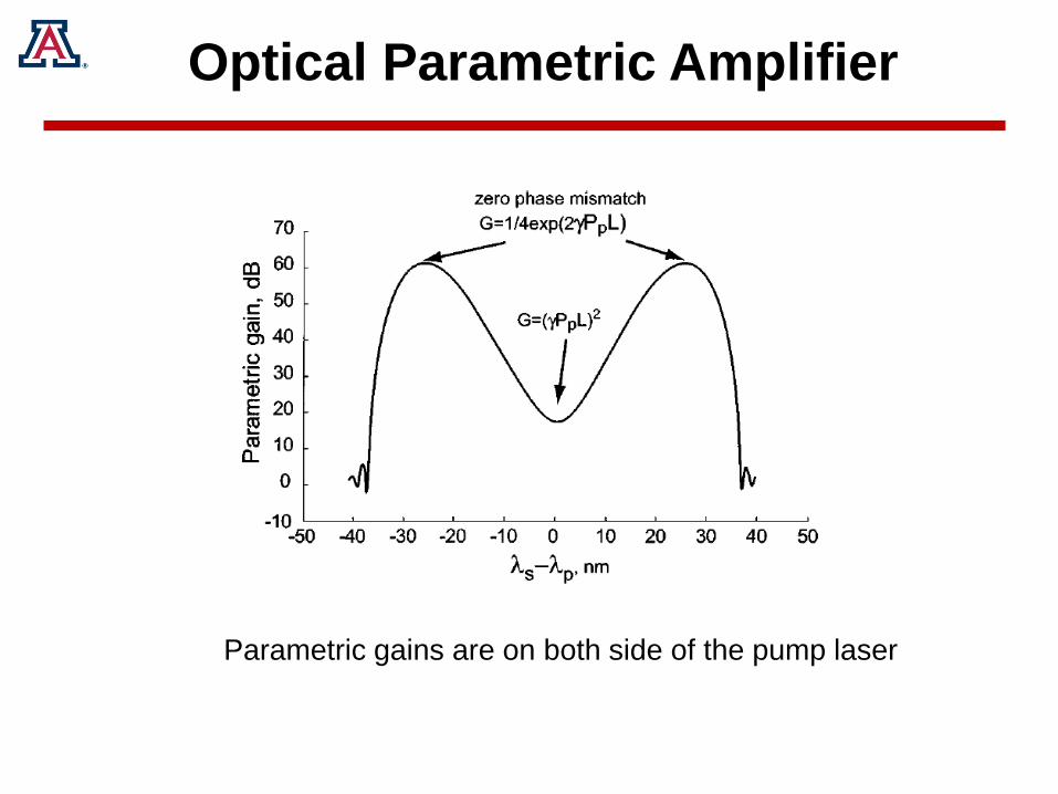
Optical Parametric Amplifier
Parametric gains are on both side of the pump laser

Optical Parametric Amplifier
FOPO with 70dB gain!
Optical Parametric Amplifier
Advantages:
• Gain bandwidth increasing with pump power
• Arbitrary center wavelength
• Very large gain (70dB)
• Unidirectional gain (no need for isolator)
• Compatibility with all-fiber devices
• High power capability
• Distributed amplification (low noise figure)

Passive fiber components
• Fiber coupler
• Variable fiber coupler
• WDM
• Isolator
• Attenuator
• Modulator
• Switches
• Pump/signal combiner
• Polarization splitter/combiner
• Collimator
• Fiber delay line
• Polarizer
• Tunable filter
• Circulator
• Faraday rotator mirror
• …

Passive fiber components
Directional couplers
WDM couplers
Isolators
Fiber spicing and connectorization

1
2
3
4
5
6
n
WD
M m
ux
1
2
3
4
5
6
n
WD
M d
em
ux
(booste
r) a
mplif
ier
transmitter
terminal
Tx
receiver
terminal
Rx
(pre
-) a
mplif
ier
(in
-lin
e)
am
plif
ier
ED
FA
ED
FA
ED
FA
transm
issio
n fib
er
transm
issio
n fib
er
dis
pers
ion
co
mp
en
sa
tio
n
dis
pers
ion
com
pe
nsation
DC DC
Ramanpump
Ramanpump
sectionspanamplifier span
transmission line
point-to-point link
SMF orNZDF
SMF orNZDF
Point-to-point WDM Transmission System
- Building Blocks -
Lasers
Brief history
Laser characteristics
Laser types
Laser modes of operation
Laser market
Fiber lasers

Longitudinal modes
,q is an integer
Allowed modes of the cavity are those where mirror separation is equal to multiple
of half wavelength.
for L >>
L
Frequency separation:
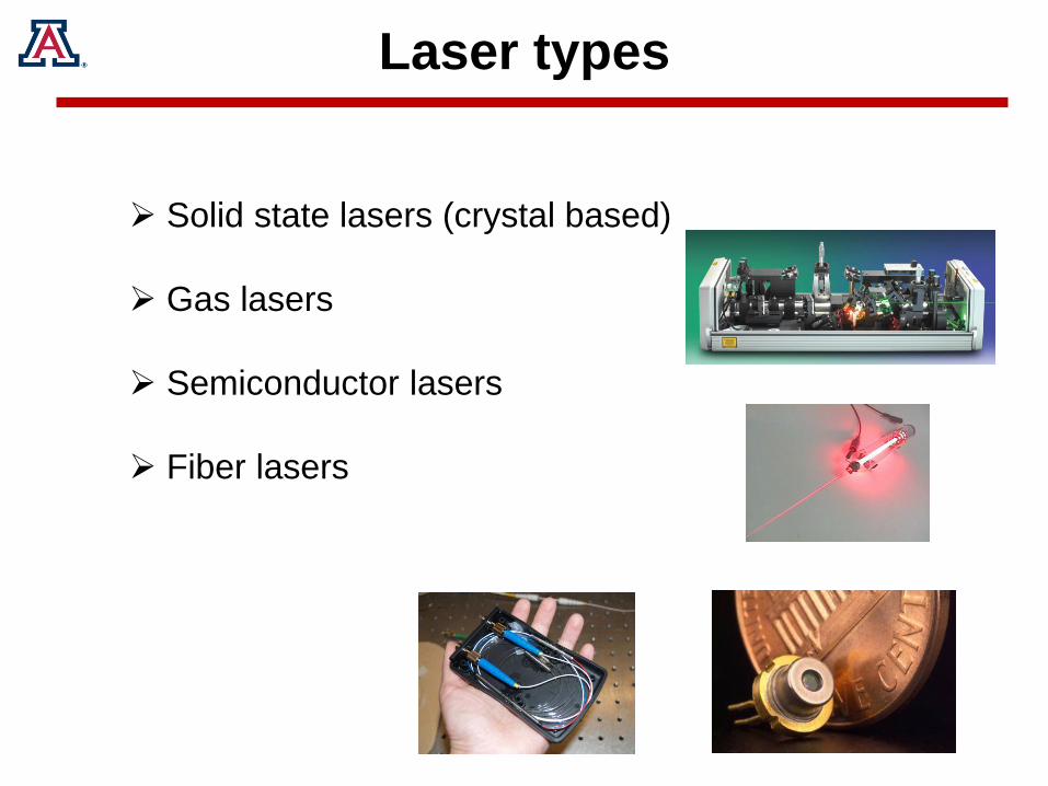
Laser types
Solid state lasers (crystal based)
Gas lasers
Semiconductor lasers
Fiber lasers
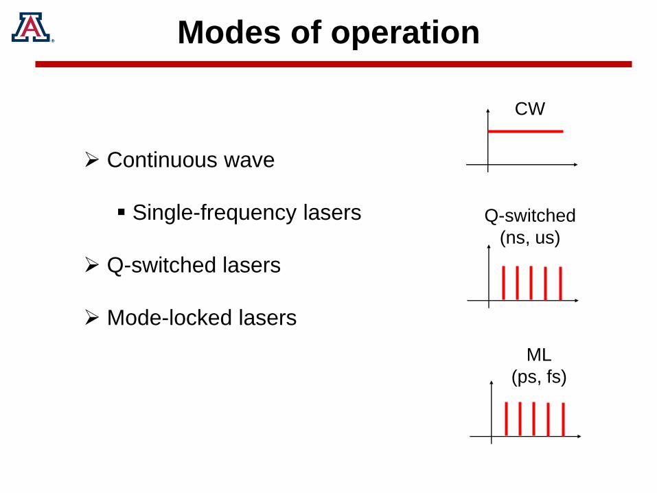
Modes of operation
Continuous wave
Single-frequency lasers
Q-switched lasers
Mode-locked lasers
CW
ML
(ps, fs)
Q-switched
(ns, us)

Semiconductor lasers
Brief history
p-n junction
Semiconductor laser based on p-n junction
Double heterostructure
Fabrication tools
Bandgap engineering
Examples of semiconductor lasers

p+ n+
EF n
(a)
Eg
Ev
Ec
Ev
Ho les in V B
Electro ns in C B
Junction
Electro nsE
c
p+
Eg
V
n+
(b)
EF n
eV
EF p
The energy band diagram of a degenerately doped p-n with no bias. (b) Banddiagram with a sufficiently large forward bias to cause population inversion andhence stimulated emission.
In vers ionreg io n
EF p
Ec
Ec
eVo
© 1999 S.O. Kasap, Optoelectronics (Prentice Hall)
Lasers based on p-n junction

Lasers based on p-n junction
• January 1962: observations of super-lumenscences in GaAs p-n junctions
(Ioffe Institute)
• Sept.-Dec. 1962: laser action in GaAs and GaAsP p-n junctions
(General Electric , IBM, Lebedev Institute)
LElectrode
Current
GaAs
GaAsn+
p+
Cleaved surface mirror
Electrode
Active region(stimulated emission region)
A schematic illustration of a GaAs homojunction laserdiode. The cleaved surfaces act as reflecting mirrors.
L
© 1999 S.O. Kasap, Optoelectronics (Prentice Hall)Wavelength
Lig
ht
inte
nsity

Lasers based on heterostructure
• p-n junction design requires cryogenic temperature to lase
• Large current density needed to create population inversion
Solution: Double Heterostructure! (DHS)
Refractiveindex
Photondensity
Active
region
n ~ 5%
2 eV
Holes in VB
Electrons in CB
AlGaAsAlGaAs
1.4 eV
Ec
Ev
Ec
Ev
(a)
(b)
pn p
Ec
(a) A doubleheterostructure diode hastwo junctions which arebetween two differentbandgap semiconductors(GaAs and AlGaAs).
2 eV
(b) Simplified energyband diagram under alarge forward bias.Lasing recombinationtakes place in the p-GaAs layer, theactive layer
(~0.1 mm)
(c) Higher bandgapmaterials have alower refractiveindex
(d) AlGaAs layersprovide lateral opticalconfinement.
(c)
(d)
© 1999 S.O. Kasap, Optoelectronics (Prentice Hall)
GaAs
Lasers based on heterostructure
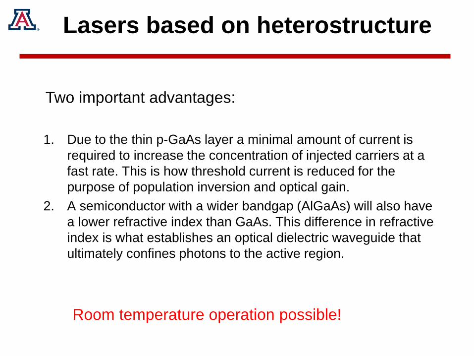
1. Due to the thin p-GaAs layer a minimal amount of current is
required to increase the concentration of injected carriers at a
fast rate. This is how threshold current is reduced for the
purpose of population inversion and optical gain.
2. A semiconductor with a wider bandgap (AlGaAs) will also have
a lower refractive index than GaAs. This difference in refractive
index is what establishes an optical dielectric waveguide that
ultimately confines photons to the active region.
Two important advantages:
Room temperature operation possible!

Lasers based on heterostructure
250 µm
120
µm
200 mA
Copper
Metal
Metal
SiO2
p Al Ga As 3 µm0.25 0.75
p Al Ga As 3 µm0.25 0.75
p GaAs 0.5 µm
p GaAs 3 µm+
n GaAs
Schematic representation of the DHS injection laser in the first CW-
operation at room temperature

LD, SLD, LED
Superluminescent diodes
(SLDs) are semiconductor
laser diodes with strong
current injection so that
stimulated emission outweighs
spontaneous emission.
Output of SLD is generally
greater than LED and lower
than LD. Spectrum is narrower
than LED and broader than
LD.
Application in sources with low
coherent time, such as optical
coherence tomography, fiber
optic gyroscopes and fiber
optic sensors
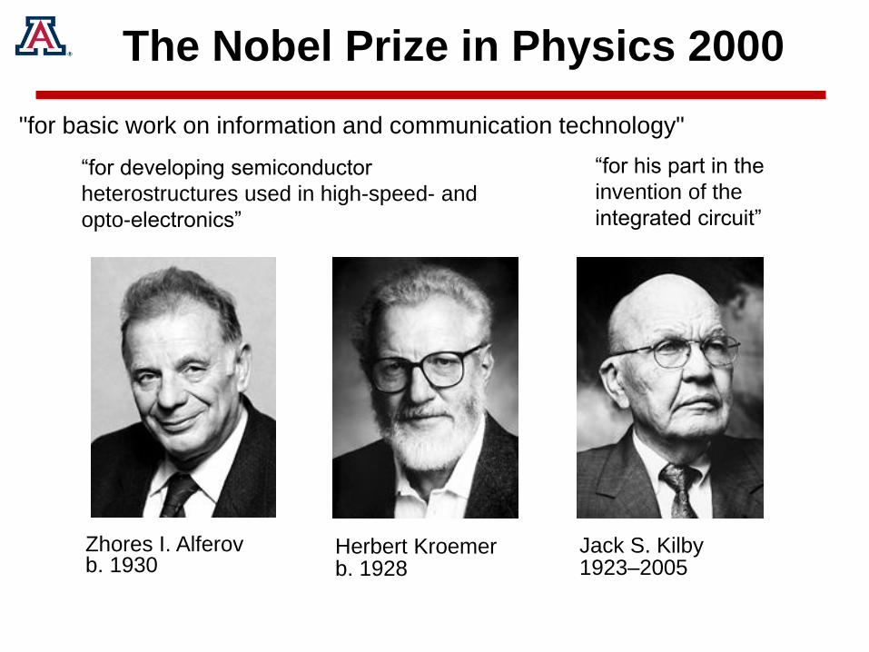
The Nobel Prize in Physics 2000
"for basic work on information and communication technology"
Zhores I. Alferov b. 1930
Herbert Kroemer b. 1928
Jack S. Kilby 1923–2005
“for his part in the
invention of the
integrated circuit”
“for developing semiconductor
heterostructures used in high-speed- and
opto-electronics”
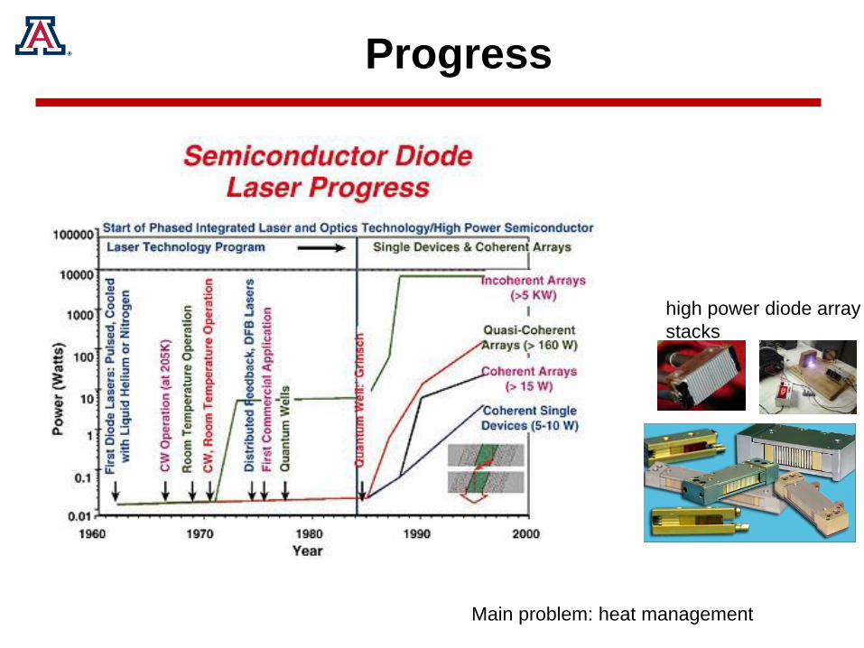
Progress
high power diode array
stacks
Main problem: heat management

Impact of dimensionality on
density of states
Lz
Lx
Lz
3D
0D
1D
2D
Ly
Lz
Lx
Egap
E00 E01
E0 E1
E000 E001
De
nsity o
f sta
tesP
N
P
N
P
N
P
N
Energy

Quantum dot: artificial atom
Atom Semiconductor Quantum dot
photon
kT
photon
valenceband
conductionband
phonon
forbidden gaps
electronlevels
holelevels
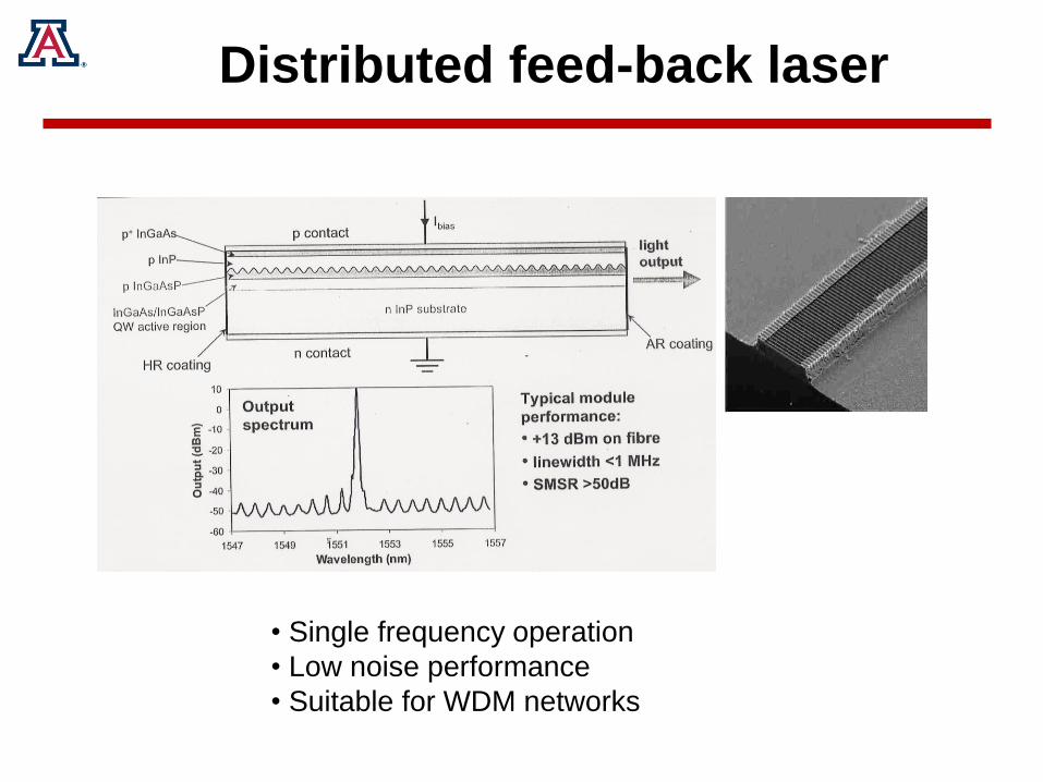
Distributed feed-back laser
• Single frequency operation
• Low noise performance
• Suitable for WDM networks
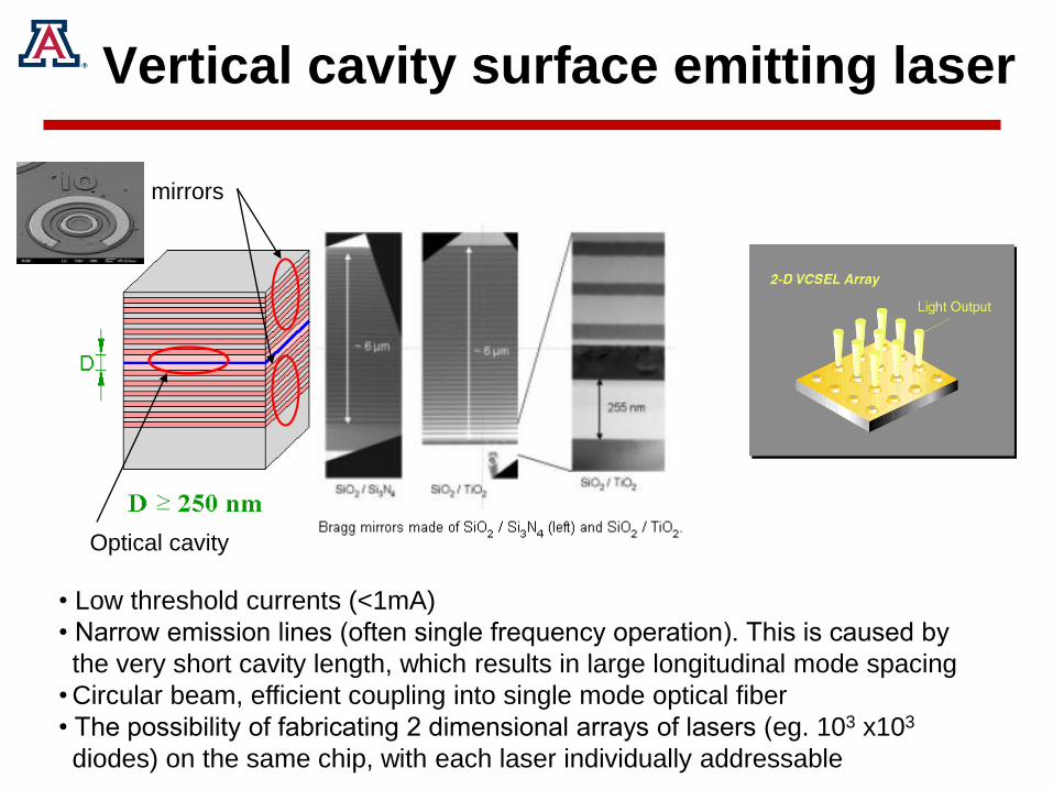
Vertical cavity surface emitting laser
Optical cavity
mirrors
• Low threshold currents (<1mA)
• Narrow emission lines (often single frequency operation). This is caused by
the very short cavity length, which results in large longitudinal mode spacing
• Circular beam, efficient coupling into single mode optical fiber
• The possibility of fabricating 2 dimensional arrays of lasers (eg. 103 x103
diodes) on the same chip, with each laser individually addressable

Photodetectors
Introduction
Most important characteristics
Photodetector types
• Thermal photodetectors
• Photoelectric effect
• Semiconductor photodetectors
Introduction
Photodetector converts photon energy to a signal, mostly
electric signal such as current (sort of a reverse LED)
Photoelectric detector
• Carrier generation by incident light
• Carrier transport and/or multiplication by current gain mechanism
• Interaction of current with external circuit
Thermal detector
• Conversion of photon to phonon
• Propagation of phonon
• Detection of phonon

Important characteristics
Wavelength coverage
Sensitivity
Bandwidth (response time)
Noise
Area
Reliability
Cost
Photoelectric effect
Absorption of photons creates carriers (electrons)
• External photoeffect: electron escape from materials
as free electrons
• Internal photoeffect (photoconductivity): excited
carriers remain within the material to increase
conductivity
Useful formula:
)(
24.1)(
eVEm
g
m
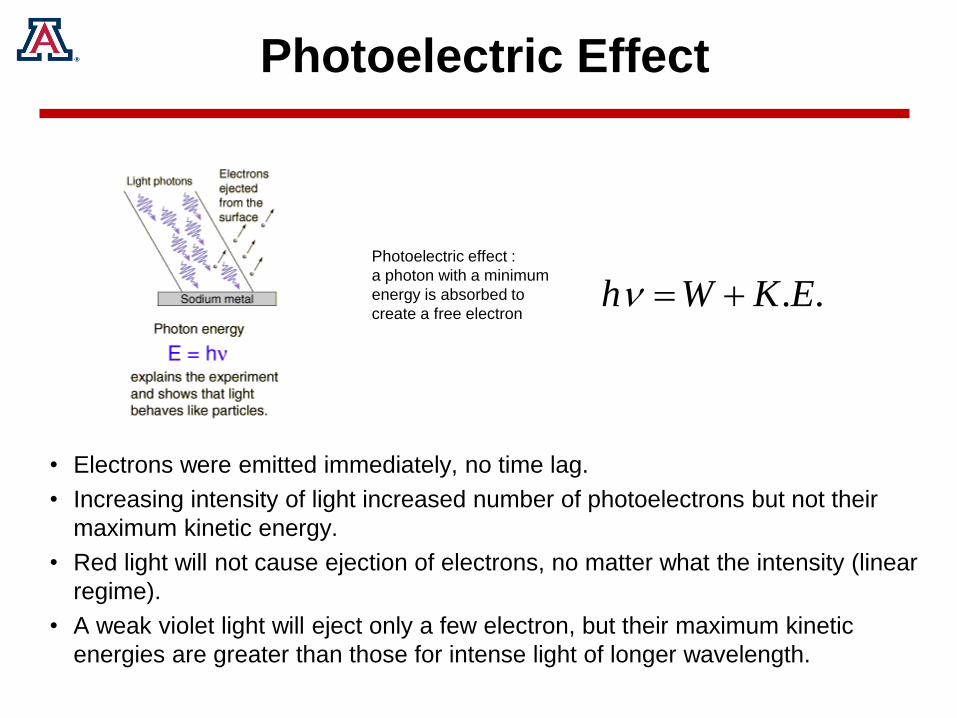
Photoelectric Effect
• Electrons were emitted immediately, no time lag.
• Increasing intensity of light increased number of photoelectrons but not their
maximum kinetic energy.
• Red light will not cause ejection of electrons, no matter what the intensity (linear
regime).
• A weak violet light will eject only a few electron, but their maximum kinetic
energies are greater than those for intense light of longer wavelength.
Photoelectric effect :
a photon with a minimum
energy is absorbed to
create a free electron..EKWh

Photo-multiplier tubes (PMT)
Vacuum photodiode operates when a photon creates a free electron at
the photocathode, which travels to the anode, creating a photocurrent.
Photocathode can be opaque (reflection mode) or semitransparent
(transmission mode).
Original electron can create secondary electrons using dynodes, with
successive higher potentials, such as a photomultiplier tube, PMT.

Photomultiplier tubes typically require 1000 to 2000 volts for proper operation. The
most negative voltage is connected to the cathode, and the most positive voltage is
connected to the anode. Voltages are distributed to the dynodes by a resistive
voltage divider, though variations such as active designs (with transistors or diodes)
are possible.
Photo-multiplier tubes (PMT)

Semiconductor photodetectors
p-n photodiode
Response time
p-i-n photodiode
APD photodiode
Noise
Wiring
Arrayed detector (Home Reading)

p-n photodetector
Photons are absorbed and e-h are generated everywhere, but only e-h in presence
of E field is transported. A p-n junction supports an E field in the depletion layer.
Region 1: e-h generated in depletion region quickly move in opposite directions
under E. External current is in reverse direction from n to p direction. Each carrier
pair generates a pulse of area e.
Region 2: e-h generated outside the depletion layer have a finite probability in
moving into the layer by random diffusion. An electron in the p side and a hole in the
n side will be transported to the external circuit. Diffusion is usually slow.
Region 3: e-h generated cannot be transported, wandered randomly, are annihilated
by recombination. No signal to external circuit.

Response time
1) Finite diffusion time: carriers take nanosecond or longer to diffuse a distance of ~ 1 µm.
2) Junction capacitance puts a limit on the intensity modulation frequency
3) Finite transit time of carriers across depletion layer
Illustration of the response of a p-
n photodiode to an optical pulse
when both drift and diffusion
contribute to the detector current:
RC
1
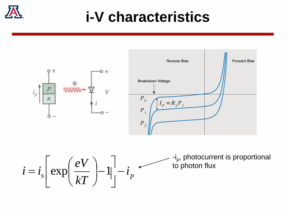
i-V characteristics
ps ikT
eVii
1exp
-ip, photocurrent is proportional
to photon flux

Modes of operation
Modes of photodiode operations: (1) open circuit (photovoltaic), (2) short circuit and
(3) reverse biased (photoconductive)
Light generated e-h pair. E field and voltage
increase with carrier. Responsivity of
photovoltaic cell is measured in V/W.
Short circuit operation. Responsivity is
typically measured in A/W.

Reversed bias mode
Reversed biased operation of a
photodiode without a load resistor.
Reversed biased operation of a
photodiode with a series load resistor.
Photodiodes are operated in strongly reversed bias mode because
1) Strong E fields give large drift velocity, reducing transit time
2) Strong bias increases depletion width, reducing capacitance
3) Increase depletion layer leads to more light collection
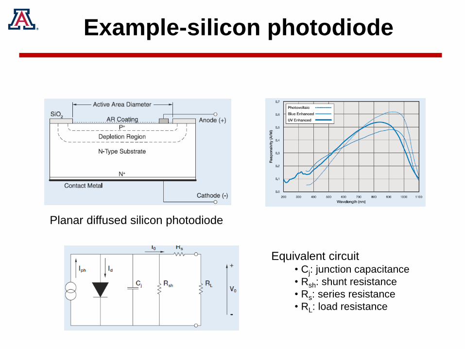
Example-silicon photodiode
Planar diffused silicon photodiode
Equivalent circuit• Cj: junction capacitance
• Rsh: shunt resistance
• Rs: series resistance
• RL: load resistance

pin photodiode
The pn junction photodiode has two
drawbacks:
• Depletion layer (DL) capacitance is
not sufficiently small to allow
photodetection at high modulation
frequencies (RC time constant
limitation).
• Narrow DL (at most a few microns)
long wavelengths incident
photons are absorbed outside DL
low QE
The pin photodiode can significantly
reduce these problems.
Intrinsic layer has less doping and wider
region (5 – 50 μm).
p+
i-Si n+
SiO2Electrode
net
eNa
eNd
x
x
E(x)
R
Eo
E
eh+
Iph
h> Eg
W
(a)
(b)
(c)
(d)
Vr
The schematic structure of an idealized pin photodiode (b) The net
space charge density across the photodiode. (c) The built-in field
across the diode. (d) The pin photodiode in photodetection is
reverse biased.
Vout
Electrode
© 1999 S.O. Kasap, Optoelectronics (Prentice Hall)

Photodiode Materials
A table below lists operating characteristics of common p-i-n photodiodes. In the parameters
the dark current is the current generated in a photodiode in the absence of any optical signal.
The parameter rise time is defined as the time over which the current builds up from 10 to
90% of its final value when the incident optical power is abruptly changed.
For Si and Ge, W typically has to be in the range of 20 – 50 µm to ensure a reasonable
quantum efficiency. The bandwidth is thus limited by a relatively long collection time. In
contrast, W can be as small as 3 – 50 µm for InGaAs photodiodes resulting in higher
bandwidths.
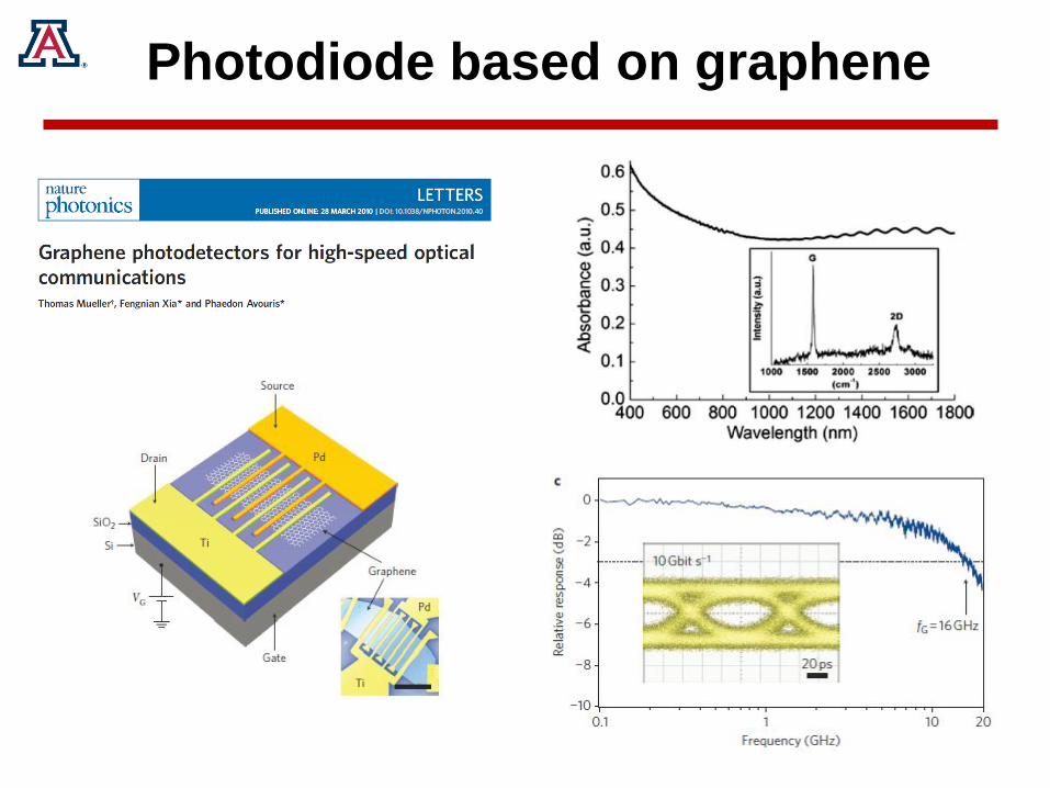
Photodiode based on graphene

Avalanche Photodiode
Avalanche photodiodes (APDs) are preferred when the amount of optical power that can be
spared for the receiver is limited. Their responsivity can significantly exceed 1 due to built in
gain. The physical phenomenon behind the gain is known as impact ionization. Under
certain conditions an accelerating electron can acquire sufficient energy to generate a new
electron-hole pair. The net result is that a single primary electron creates many secondary
electrons and holes, all of which contribute to the current.
The generation rate is governed by two parameters, αe and αh, the impact-ionization
coefficients for electrons and holes, respectively. Their numerical values depend on the
semiconductor material and on the electric field that accelerates electrons and holes. Figure
below shows the coefficients for several semiconductors.
The values for αe and αh ~ 1x10⁻⁴
cm-1 are obtained for electric fields
in the range of 2 – 4 x 10⁵ V/m.
Such high fields are obtained by
applying a high voltage of ( ~ 100
V) to the APD. These values
decreases with increasing
temperature.

Avalanche Photodiodes
h+
n+ p
e–
Avalanche region
E
e-
h+
Ec
Ev
Impact ionization processes resulting
avalanche multiplication
Impact of an energetic electron's kinetic energy
excites VB electron to the CV.
p+
SiO2Electrode
x
x
E(x)
R
h> Eg
p
Iphoto
e– h+
Absorption
region
Avalanche region
Electrode
n+
E
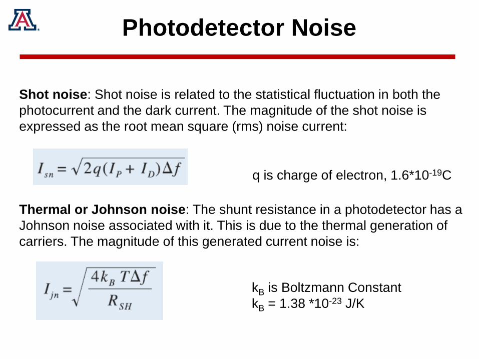
Photodetector Noise
Shot noise: Shot noise is related to the statistical fluctuation in both the
photocurrent and the dark current. The magnitude of the shot noise is
expressed as the root mean square (rms) noise current:
Thermal or Johnson noise: The shunt resistance in a photodetector has a
Johnson noise associated with it. This is due to the thermal generation of
carriers. The magnitude of this generated current noise is:
q is charge of electron, 1.6*10-19C
kB is Boltzmann Constant
kB = 1.38 *10-23 J/K

Photodetector Noise
Noise Equivalent Power (NEP)
Noise Equivalent Power is the amount of incident light power on a
photodetector, which generates a photocurrent equal to the noise
current. NEP is defined as:
Total Noise
The total noise current generated in a photodetector is determined by:
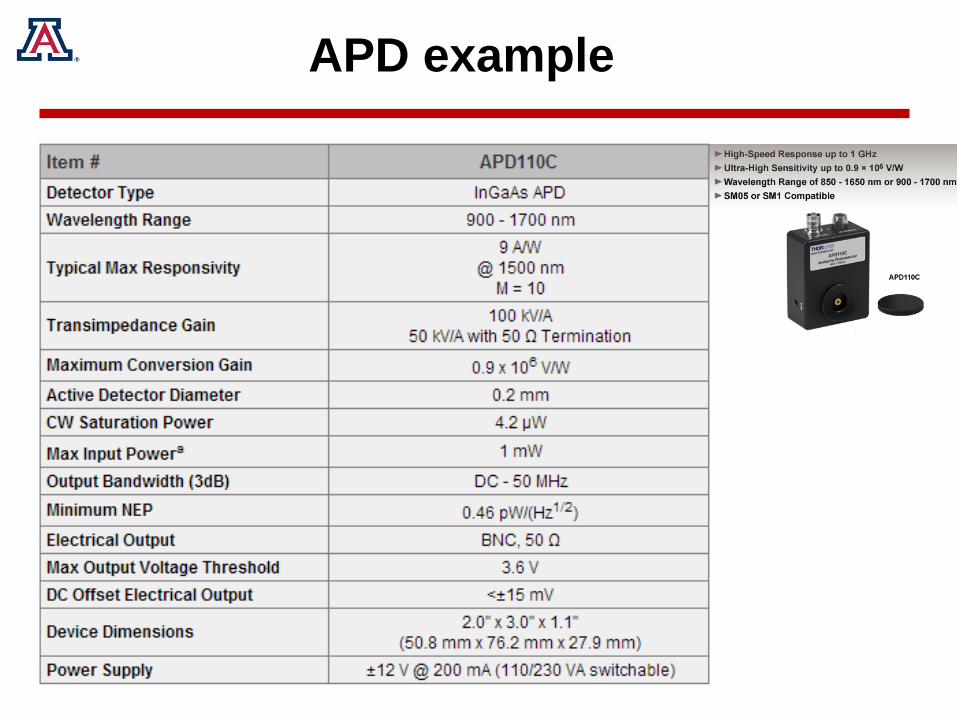
APD example
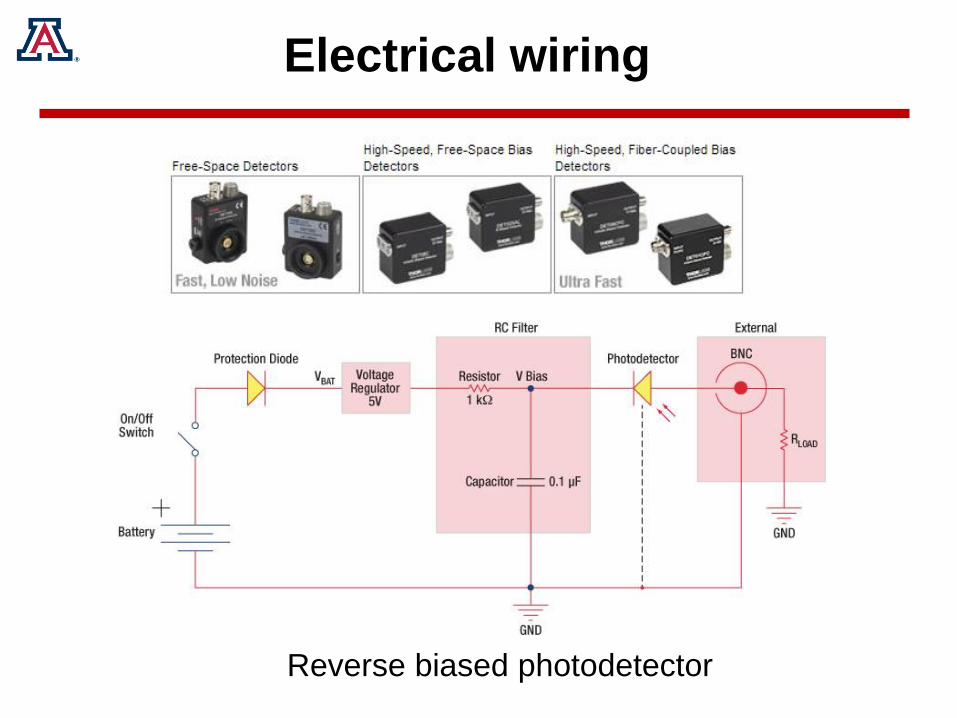
Electrical wiring
Reverse biased photodetector
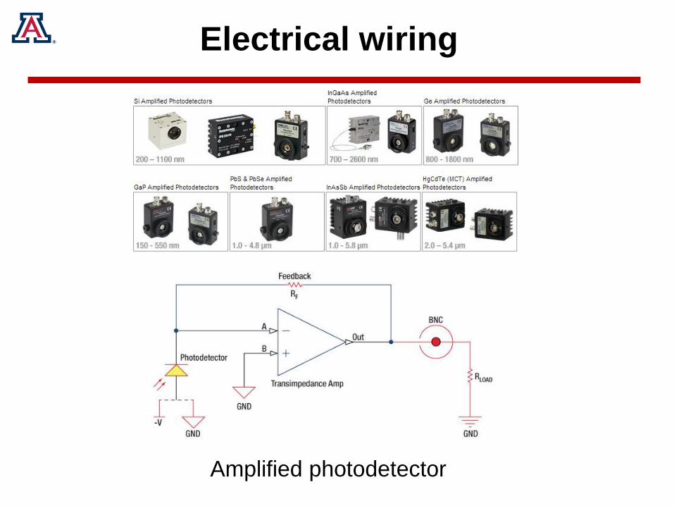
Electrical wiring
Amplified photodetector

Introduction to Network
Modulation formats
Signal multiplexing
• Time
• Code
• Wavelength
System performance
• Bit Error Rate
• Optical signal to noise ratio
• Eye diagram
Network architecture, limitation
CIAN
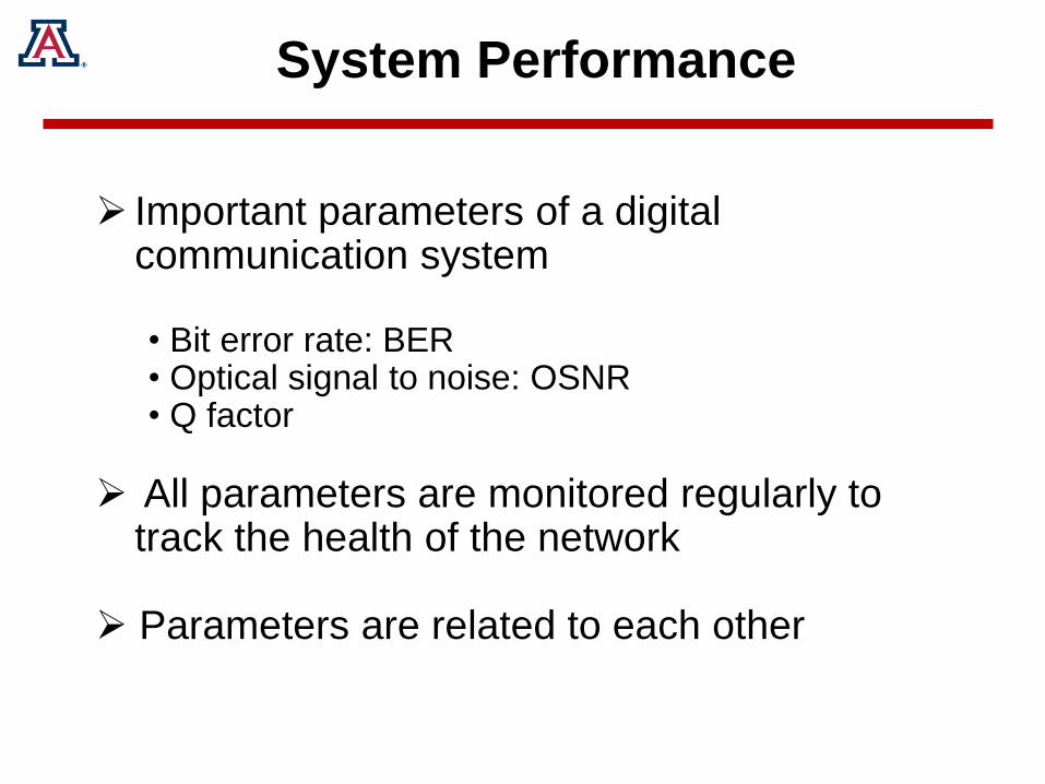
System Performance
Important parameters of a digital communication system
• Bit error rate: BER• Optical signal to noise: OSNR• Q factor
All parameters are monitored regularly to track the health of the network
Parameters are related to each other

Bit Error Rate
Bit error rate (BER): One of the most important ways to determine the
quality of a digital transmission system is to measure its Bit Error Rate
(BER). BER is calculated by comparing the transmitted sequence of
bits to the received bits and counting the number of errors. The ratio of
how many bits received in error over the number of total bits received
is the BER. This measured ratio is affected by many factors including:
signal to noise ratio, distortion, and jitter.
BER = Nerr/Nbits
For a good system performance BER < 10-12

Bit Error Testing-Eye diagram
An eye diagram is a common indicator of the quality of signals in high-speed digital transmissions.
An oscilloscope generates an eye diagram by overlaying sweeps of different segments of a
long data stream driven by a master clock.
In practical terms this may be achieved by displaying the data
waveform on a sampling oscilloscope triggered from the system clock.

Q-factor
The performance of digital fiber-optic transmission systems can be specified
using the Q-factor. The Q-factor is the electrical signal-to-noise ratio (SNR) at
the input of the decision circuit in the receiver terminal Rx.
For the purpose of calculation, the signal level is interpreted as the difference
in the mean values 0 and 1, and the noise level is the sum of the standard
deviations 0 and 1 at the sampling time:
Q-factor
Bit Error Testing-Eye diagram
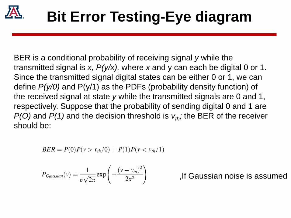
BER is a conditional probability of receiving signal y while the
transmitted signal is x, P(y/x), where x and y can each be digital 0 or 1.
Since the transmitted signal digital states can be either 0 or 1, we can
define P(y/0) and P(y/1) as the PDFs (probability density function) of
the received signal at state y while the transmitted signals are 0 and 1,
respectively. Suppose that the probability of sending digital 0 and 1 are
P(O) and P(1) and the decision threshold is vth; the BER of the receiver
should be:
,If Gaussian noise is assumed

Bit Error Testing-Eye diagram
The probability for the receiver to declare 1 while the transmitter actually sends a 0 is:
,Where ,Q-value or quality factor
Similarly, the probability for the receiver to declare 0 while the transmitter actually sends a 1 is:
,P(0) = P (1) = 0.5
is assumed

Bit Error Testing-Eye diagram
A widely used mathematical function, the error function, is defined as:
And the complementary error function is defined as:

Bit Error Testing-Eye diagram
By symmetry, we can assume Q1 = Q0 = Q, or
,where
BER as the function of the Q-value


