Volume 99, Number 5, September-October 1994 Journal of Research of the National Institute of Standards and Technology [J. Res. Natl. Inst. Stand. Technol. 99, 605 (1994)] Optical Characterization in Microelectronics Manufacturing Volume 99 Number 5 September-October 1994 S. Perkowitz' and D. G. Seller National Institute of Standards and Technology, Gaithersburg, MD 20899-0001 and W. M. Duncan Texas Instruments, Inc., Dallas, TX 75243 To successfully construct semiconductor devices, the semiconductor industry must measure fundamental material parameters, especially when developing new materials; measure the quality of the material as it is grown; accutate\y determine the details of thin films, quantum wells, and other microstruc- tures that control or affect device per- formance; and measure properties of the devices themselves. Properties that need to be determined, therefore, in- clude basic band structure and trans- port parameters, such as energy gap values and carrier scattering times; the presence and concentration of impuri- ties and defects; alloy parameters; layer thicknesses; the distribution of materi- als in complex structures; and many others. This process of determining a wide range of material, structural, and device parameters is called characteri- zation. The semiconductor industry uses many characterization methods which draw on electrical, chemical, and other approaches. Among these, optical char- acterization techniques, defined as those using electromagnetic radiation from the ultraviolet to the far infrared, stand out because they are nondestruc- tive and require minimal sample prepa- ration since no contacts are needed. These features are of great importance for production use or to examine fin- ished devices. Another benefit is that, unlike electrical methods which require fixed contacts, optical techniques can give two- or three-dimensional maps of properties over the extent of a semi- conductor wafer. The six techniques de- scribed in this paper (ellipsomctry, infrared spcctroscopy, microscopy, mod- ulation spectroscopy, photoluminesccncc, and Raman scattering) were chosen be- cause they arc currently or potentially widely used in the industry; they mea- sure a broad array of semiconductor parameters; and they operate in differ- ent regions of the electromagnetic .spec- trum. The di.scussion of each technique indicates the basic semiconductor quan- tities measured, gives the scientific basis of the technique, and indicates how the measurement is made. Illustrative ex- amples from the literature arc discussed in detail, showing applications to im- portant semiconductor materials. More information can be obtained from the detailed list of references included. Key words: ellipsomctry; infrared .spec- troscopy; modulalicm spectroscopy; optical microscopy; photoluminescence; Raman scattering. Accepted: July 21, 1994 Contents 2. Introduction 606 Ellipsometry ^^^ ' Consulting scientist. Present address: Department of P'^y^J"' Rollins Research Center, Emory University, Atlanta, GA .3U3..2- 2430. 3. Infrared Spectroscopy... • 4. Optical Microscopy 5. Modulation Spectroscopy. 6. Photoluminescence 7. Raman Scattering 612 617 623 627 634 605
Transcript
Volume 99 Number 5 September-October 1994
Journal of Research of the National Institute of Standards and Technology
[J Res Natl Inst Stand Technol 99 605 (1994)]
Optical Characterization in Microelectronics Manufacturing
Volume 99 Number 5 September-October 1994
S Perkowitz and D G Seller
National Institute of Standards and Technology Gaithersburg MD 20899-0001
and
W M Duncan
Texas Instruments Inc Dallas TX 75243
To successfully construct semiconductor devices the semiconductor industry must measure fundamental material parameters especially when developing new materials measure the quality of the material as it is grown accutatey determine the details of thin films quantum wells and other microstruc- tures that control or affect device per- formance and measure properties of the devices themselves Properties that need to be determined therefore in- clude basic band structure and trans- port parameters such as energy gap values and carrier scattering times the presence and concentration of impuri- ties and defects alloy parameters layer thicknesses the distribution of materi- als in complex structures and many others This process of determining a wide range of material structural and device parameters is called characteri- zation The semiconductor industry uses many characterization methods which draw on electrical chemical and other approaches Among these optical char- acterization techniques defined as those using electromagnetic radiation from the ultraviolet to the far infrared stand out because they are nondestruc- tive and require minimal sample prepa- ration since no contacts are needed These features are of great importance
for production use or to examine fin- ished devices Another benefit is that unlike electrical methods which require fixed contacts optical techniques can give two- or three-dimensional maps of properties over the extent of a semi- conductor wafer The six techniques de- scribed in this paper (ellipsomctry infrared spcctroscopy microscopy mod- ulation spectroscopy photoluminesccncc and Raman scattering) were chosen be- cause they arc currently or potentially widely used in the industry they mea- sure a broad array of semiconductor parameters and they operate in differ- ent regions of the electromagnetic spec- trum The discussion of each technique indicates the basic semiconductor quan- tities measured gives the scientific basis of the technique and indicates how the measurement is made Illustrative ex- amples from the literature arc discussed in detail showing applications to im- portant semiconductor materials More information can be obtained from the detailed list of references included
Journal of Research of the National Institute of Standards and Technology
1 Introduction
To successfully construct semiconductor devices the microelectronics industry must measure funda- mental material parameters especially when devel- oping new materials measure the quality of the material as it is grown accurately determine the structural details of thin films quantum wells and other microstructures at the heart of devices and measure properties of the devices themselves Prop- erties that need to be determined therefore include basic band structure and transport parame- ters such as gap values and carrier scattering times the presence and concentration of impurities and defects alloy parameters layer thicknesses the dis- tribution of materials in complex structures and many others
The semiconductor industry uses many charac- terization methods which draw on electrical chem- ical and other approaches Among these optical characterization techniques defined as those using electromagnetic radiation from the ultraviolet to the far infrared stand out because they are nonde- structive and require minimal sample preparation since no contacts are needed These features are of great importance for production use for on-line ap- plications and for examination of finished devices Another benefit is that optical techniques can give two- or three-dimensional maps of properties over the extent of a semiconductor wafer without requir- ing fixed contacts
Six techniques are described in this paper (ellip- sometry infrared spectroscopy optical microscopy modulation spectroscopy photoluminescence and Raman scattering) They were chosen because they are currently widely used in the industry and be- cause they measure a broad array of semiconductor parameters The discussion of each technique indi- cates the basic semiconductor quantities measured (see Table 1) the physical basis of the technique and how the measurement is made Illustrative ex- amples from the literature are discussed showing applications to important semiconductor material systems A more detailed review of infrared Raman and photoluminescence speclroscopies is given in a book by Perkowitz [1] A recent review of the optical properties of semiconductors is given bv Amirlharaj and Seller [2]
11 A Note on Units
Some regions of the electromagnetic spectru and some optical methods refer to wavelength a
spectrum as a
matter of usage others use wavenumbers or photon energy Each section here uses the most common units for that technique including wave- length in nanometers (nm) and micrometers (ixm) wavenumber in cm and photon energy in elec- tron volts (eV) Table 2 shows conversion factors for the main units of measure usually encountered
Table 1 Semiconductor quantities (horizontal rows) and opti- cal characterization methods (vertical columns labeled as fol- lows ELL cllipsometry IR infrared spectroscopy MIC microscopy MOD modulation spectroscopy PL photolumines- cence and RAM Raman scattering) A bullet at the intersection of a given row and column means that the parameter can be de- termined by that technique using conventional methodology Further details are given in the discussion
ELL IR MIC MOD PL RAM
Carrier density bull bull
Carrier mobility bull
Carrier scattering bull bull time
Composition bull bull bull bull bull
Crystal orientation
Crystallinity bull bull bull
Defects bull bull bull
Energy gap bull bull bull
Film thickness bull bull bull
Impurities bull bull bull bull
Resistivity bull
Stress bull bull bull bull bull
If the effective mass is known Time resolved
Table 2 Conversion factors for units of measure
Anm = lO^Ajim
poundeV = 12397(Ajim)
= 12397xlO-A-cm-
A-cm- = 10V(AjjLm)
12 References
[I] S Perkowitz Optical Characterization of Semiconductors Infrared Raman and Photoluminescence Spectroscopy
Academic Press London (1993) [2] P Amirlharaj and D G Seller Optical Properties of Semi-
conductors Chapter in Handbook of Optics McGraw-Hill to be published
606
Volume 99 Number 5 Scptember-Octohcr 19M
Journal of Research of the National Institute of Standards and Technology
2 Ellipsometry
21 Introduction
Ellipsometry is a technique widely used to mea- sure the thicknesses of films important to semicon- ductor technology such as SiOz on Si Thicknesses measured are typically in the range of several nm to several hundred nm Surface cleanliness of semi- conductor wafers during processing can also be de- termined In spectroscopic ellipsometry the ellipsometric data are obtained as a function of wavelength Then appropriate modeling and fitting can yield the dielectric functions and thicknesses of the layers in complex semiconductoroxide multi- layer systems such as SIMOX (Separation by IM- planted OXygen) a silicon-on-insulator material formed by high-energy oxygen ion implantation in silicon The dielectric functions give a complete pic- ture of composition for the entire layered structure
22 Physical Basis
Ellipsometry is based on the polarization trans- formation that occurs when a beam of polarized light is reflected from (or transmitted through) an interface or film For example if plane- or linearly- polarized light impinges on the surface of an ab- sorbing medium the reflected light usually becomes elliptically polarized because the reflection process differently affects the in-plane component of the in- cident electric field Ep relative to the perpendicular electric field component Es Each component is re- flected with new values of amplitude and phase The key parameters obtained from an ellipsometric measurement are the ellipsometric angles lA and A These appear in the complex reflection ratio p
defined as
p = ^ = tan(A)e (^^
Where the amplitude reflection coefficients r and
(2)
n are
_ poundp (reflected] P ~ Ep (incident)
_ pound5_(reflected) poundbull (incident)
(3)
as The ellipsometric angles are defined 0 = tan-U and zl is the difference m phase be
tvveen the p and s components
23 Experimental and Technical Details
Ellipsometric measurements stirt with light of known polarization incident on the sample The po- larization of the reflected light is determined from which further analysis gives the parameters such as refractive index and film thickness which determine the interaction between light and sample
In its simplest form singlc-wavelcnglli cilipsonic- try requires a manual nulling to gather data Light from the source (usually a laser for single-wave- length work) passes through a linear polarizer then through a compensator which elliptically polarizes the light The light continues to the sample is re- flected passes through a polarization annlycr and is finally detected The null technique works by ad- justing the angle of the polarizer with respect to compensator sample and analyzer until the reflec- tion process just cancels the eliipticiiy the light gained from the compensator Then the reflecled light is linearly polarized and can he extinguished by choosing the appropriate angle for the analyzer that is until the photomultiplier shows a minimum signal The two values of the angles yield gt
This null process is too slow for real-time mea- surements or for spectroscopic ellipsometiy I hrec types of automatic ellipsometry (self-compensating rotating element and polarization-modulated) to- cether with dedicated computers allow rapid mea- surement and analysis In the automatic elf-compensating system [ 1 ]he angles of e -
early polarized light leaving the polarizer andcn-
edng the analyzer are rotated by NnKlay o Pokels cells until the null is achieved I his type
Ls ument can give fixed wavelength data w hin smd spectroscopic data over a wide wavelenglh
X optical lavout of the rotating element system
^^rnriis or ti reflected tbeam a flxed angular velocity typically cor- light beam ai ^^^^ ^^^_^g bdquo
responding 0 0 H^^^j signal wbdquoh two
yer -laquoJP bdquobdquobull bdquona every rotation if maxima and two true ^^^ ^nipijclly he light were ^y I^^^ f ^f f ine-squarcd polarized ligh l^yj f nonzeri mm-
5 ms
607
Volume 99 Number 5 September-October 1994
Journal of Research of the National Institute of Standards and Technology
Lamp
3 Polarizer
ymdashAperture
L rij (Compensator)
Sample
Aperture
Photomultiplier
(a) 00051 pF
Photo- multiplier
Sample hold Reset
Reference
(b)
Fig 1 Schematic diagrams of (a) optical elements and (b) sig- nal processmg system for a rotating analyzer spectroscop c llip-
laquo)meter designed for high-precision measurementsof the optcal
^3 p1ot2 bull ^ bull deg==^^ ^^^ ^deg- (S
r^ [f n- ^P deg^ ^^^^ ^^ polarization- modulated elhpsometer [1] where the compensator n the manual null system is replaced by a birefrin- gent phase tnodulator (a piezobirefringent plate or a Pockels cell) In the phase modulator the elliptic ty mparted to the linearly polarized light varLs muscdally wth time rather than remaining con
stant as n the self-compensating system The signal v^htch results at the detector can be Fourier ana lyzed or analyzed by a phase-sensitive detector to
give p A piezobirefringent modulator is a fast device which can operate at 100 kHz or more hence this system can obtain data in an interval of 10 ms per wavelength measurement which means that full scans over the range 400 nm to 700 nm can be obtained in a few seconds or less
Of the three automatic systems the polarization- modulated spectrometer is best for real-time rapid data acquisition However in the self-compensating and polarization-modulation cases the compensa- tor or modulator must be tuned for each wave- length hence these are more complex and can be less accurate than the rotating analyzer system
For spectroscopic ellipsometry a stable xenon lamp with output covering the near ultraviolet to near infrared is a commonly used source The sam- ple is mounted on a high-accuracy stage to allow careful angle alignment Usually an autocollimator and apertures are used to control collimation and alignment In general available equipment gives good results over the near infrared to the near ul- traviolet The ellipsometric angles 4 and i( can be measured to within millidegrees resulting in uncer- tainties of less than one part in 10^ for the index of refraction and tenths of a nanometer for the corre- sponding thicknesses
Parameters for a complex semiconductoroxide system examined by ellipsometry are determined by sophisticated computer software [1-2] These fit the measured ellipsometric parameters versus wave- length by assuming appropriate dielectric functions for each layer and layer thicknesses Commercial systems include appropriate software and fitting routines are also available from other sources
24 Illustrative Applications
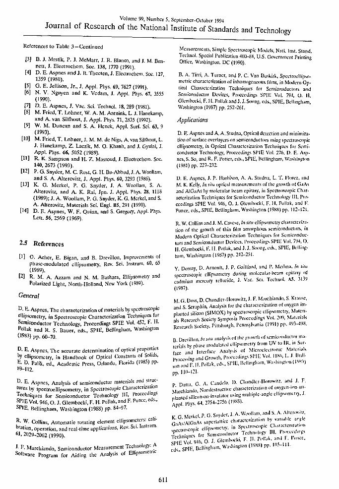
An example of the kind of semiconductor analysis that can be achieved with spectroscopic ellipsome- try is shown in Fig 2 for a sample of SIMOX an important silicon-on-insulator system The ellipso- metric angles ^ and i show complex spectra over the range 15 eV to 45 eV with the large oscilla- tions related to interference effects Multiparame- ter regression analysis yields the fits displayed in the plots which determine the samples structural de- tails as shown
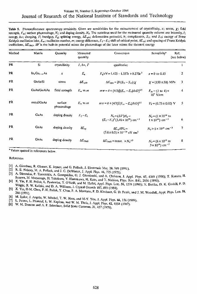
Table 3 presents typical sensitivities of quantities obtained by ellipsometry such as thicknesses com- position and temperature For more specific de- tails the reader can refer to the citations given in the table
608
Volume 99 Number 5 September-October 1994
Journal of Research of the National Institute of Standards and Technology
Sample 802
SiOg (140plusmn03)A
c-Si (2288plusmn02) A
SiOj (3340128) A
c-SiSiO2(306plusmn10)A 047 plusmn003
20 25 30 35 40 45
SiOp (140plusmn03)A
C-Si (2288plusmn02) A
SiOj (3340128) A
c-SiSiOj (306110) A 0471003
0 15 2 0 25 30
PHOTON ENERGY (eV)
Pi 2 Ellipsometric angles ^^^f-^ jS ^^-P^^s^^ Individual points data btaned from ro aung ^^^^^^^_ ^^^^^ ^^ ^^j
Solid line ft obtained by ^-^g^fdeg 7^^^-cly bclcw the 334 nm SiO bycr composition shown on the right The lagt^ ^J bdquo j siO with 47 volume is modeled as a granular --^X Shown to the right of the figure arc fraction c-Si using effecfve -^^ ^ S^ertainties of the model parameter the thicknesses of the layers The ^ff^ ^ ^ ^ he regression analysis (After are set to one standard devtanon as termmc^^ y^^^_ ^^ ^^^ ^^ ^^ bdquo bdquo
D Chandler-Horowitz et al (1991) P dards and Technology)
609
Volume 99 Number 5 September-October 1994
Journal of Research of the National Institute of Standards and Technology
Table 3 Spectral ellipsometry sensitivity Given are sensitivities for the measurement of thicknesses composition damage profile and temperature in a number of systems The notations used for the measured quantity column are the complex reflection ratio p the amplitude ratio ir and the phase shift J
Method Matrix Quantity Measured quantity
Conversion Sensitivity Ref (see
below)
SE Si02Si Si02 thickness P Fresnel Equations^ and Estimator^^
(FEampE)
plusmn02 A to plusmn06 A 1000 A to 2300 A
3
SE Si02Si02 +SiSi Interfacial SiOz + Si thickness
P FEampE and EMA
plusmn2 A7A 4
SE Si02Si02 +SiSi SiO thickness P FEampE and EMA
(11121+02) A and (2769 plusmn02) A
5
SE SiOa-Sic-Si + SiCSiCc-Si Layer thicknesses
P FEampE and EMA plusmn2 A to plusmn25 A 6
SE Polysilicon Polysilicon composition (eg void + c-Si + a-Si)
P FEampE and EMA c-Si 014 plusmn002 void 025 plusmn006
7
SE Si Damage profile P FEampE and EMA Damage range (170 plusmn50) A to
(320 plusmn20) A
8
SE SiOpolysiliconSi02Si Polysilicon and Si02
thicknesses
P FEampE and EMA Native oxide (15 plusmn03) A Poly plusmn03 A to plusmn39 A (240 to 1030) A
Oxide plusmn04 A to plusmn17 A (50 to 130) A
9
SE SiOjSiSiNSi Native oxide Si and nitride
thickness
P FEampE and EMA - 10
SWE SiOySi Temperature -A 4 polynomial plusmn10degC 11
VASE OxideGaAs AIGaiAs
GaAs
Thicknesses and AlGaAs composition
P FEampE and EMA Oxide (34 plusmn3) A GaAs (159 plusmn8) A
AlGaAs (865 plusmn14) A AlGaAs A =035 plusmn002
12
VASE OxideGaAs AUGa-As
GaAsAlGaAs-GaAs
Thicknesses and AlGaAs composition
P FEampE and EMA Oxide (26plusmn1) A GaAs (435 plusmn8) A
AtraAgt M13 + 14i A
13
SE AlGa_AsGaAs AlGaAs composition
and thickness in silit
Trajectories in poundi and euro2
AlGaAs x= 037 plusmn0005 GaAs(142plusmn10) A AlGaAsGaAs SLS
5 (470 plusmn20) A AlGaAsGaAs SLS
J = 032 plusmn0001
x= 02 plusmn003 (xgt02)
Typically calculated as the 90 mnMci^c^l^^^^ZJZZrZ mterval from the mean square deviation and covariancc matrix
References
[2] a ^^pSTa ThtLanlRH rr Tv -s ^orh Holland Amsterdam (1989) Ch r n vnang j Vac Sci Tcchnol 16 1374 (1979)
14
610
Volume 99 Number 5 September-October 1994
Journal of Research of the National Institute of Standards and Technology
References to Table 3-Continued
[3] B J Mrstilc P J McMarr J R Blanco and J M Ben- nett J Electrochem Soc 138 1770 (1991)
[4] D E Aspnes and J B Theeten J Electrochem Soc 127 1359 (1980)
[5] G E Jellison Jr J Appl Phys 69 7627 (1991) [6] N V Nguyen and K Vedam J Appl Phys 67 3555
(1990) [7] D E Aspnes J Vac Sci Technol 18 289 (1981) [8] M Fried T Lohner W A M Aarnink L J Hanekamp
and A van Silfhout J Appl Phys 71 2835 (1992) [9] W M Duncan and S A Henck Appl Surf Sci 63 9
(1993) [10] M Fried T Lohner J M M de Nigs A van Silfhout L
J Hanekamp Z Laczik M Q Khanh and J Gyulai J Appl Phys 66 5052 (1989)
[11] R K Sampson and H Z Massoud J Electrochem Soc 140 2673 (1993)
[12] P G Snyder M C Rost G H Bu-Abbud J A Woollam and S A Alterovitz J Appl Phys 60 3293 (1986)
[13] K G Merkel P G Snyder J A Woollam S A Alterovitz and A K Rai Jpn J Appl Phys 28 1118 (1989) J A Woollam P G Snyder K G Merkel and S A Alterovitz Materials Sci Engl B5 291 (1990)
[14] D E Aspnes W E Quinn and S Gregory Appl Phys Lett 56 2569 (1969)
25 References
[1] O Acher E Bigan and B Drevillon Improvements of phase-modulated ellipsometry Rev Sci Instrum 60 65 (1989)
[2] R M A Azzam and N M Bashara Ellipsometry and Polarized Light North-Holland New York (1989)
General
D- E Aspnes The characterization of materials by spectroscopic ellipsometry in Spectroscopic Characterization Techniques for Semiconductor Technology Proceedings SPIE Vol 452 F H Pollak and R S Bauer eds SPIE Bellingham Washington (1983) pp 60-70
D- E Aspnes The accurate determination of optical properties ^ ellipsometry in Handbook of Optical Constants of Solids E- D- Palik ed Academic Press Orlando Florida (1985) pp 89-112
D E Aspnes Analysis of semiconductor materials and struc- tures by spectroellipsometry in Spectroscopic Characterization Techniques for Semiconductor Technology III Proceedings SPIE Vol 9460 J Glembocki F H Pollak and F Ponce eds SPIE Bellingham Washington (1988) pp 84-97
R- W Collins Automatic rotating element cllipsomcters cali- bration operation and real-time applications Rev Sa Instrum
61 2029-2062 (1990)
J- F Marchiando Semiconductor Measurement Technology A Software Program for Aiding the Analysis of Ellipsomctric
Measurements Simple Spectroscopic Models Natl Inst Stand Technol Special Publication 400-84 US Government Printing Office Washington DC (1990)
B A Tirri A Turner and P C Van Buskirk Speclrocllipso metric characterization of inhomogcneous films in Modern Op- tical Characterization Techniques for Semjconduclors and Semiconductor Devices Proceedings SPIE Vol 794 O H Glembocki F H Pollak and J J Soong eds SPIE Bellingham Washington (1987) pp 252-261
Applications
D E Aspnes and A A Studna Optical detection and minimiza- tion of surface overlayers on semiconductors using spectroscopic ellipsometry in Optical Characterization Techniques for Semi- conductor Technology Proceedings SPIE Vol 276 D E Asp- nes S So and R F Potter eds SPIE Bellingham Washington (1981) pp 227-232
D E Aspnes J P Harbison A A Sludna L T Morcz and M K Kelly In situ optical mcasuremenis of the growth of GaAs and AIGaAs by molecular beam epitaxy in Spectroscopic Char- acterization Techniques for Semiconductor Technology III Pro- ceedings SPIE Vol 946 O J GlemlxKki F H Pollak and I Ponce eds SPIE Bellingham Washington (19H8) pp 112-121
R W Collins and J M Cavesc In silii ellipsometry charactcrira- tion of the growth of thin film amorphous scmicondiiclors in Modern Optical Characterization Techniques for Semiconduc- tors and Semiconductor Devices Proceedings SPIE Vol 794 O H Glembocki F H Pollak and J J Sining eds SIIF Belling- ham Washington (19S7) pp 242-251
Y Demay D Arnoult J P Gailliard and P Medina In iilu spectroscopic ellipsometry during molecular-beam epitaxy of cadmium mercury tclluride J Vac Sci Technol S MV)
(1987)
M G Doss D Chandler-Horowitz J F Marchiando S Krausc and S Scraphin Analysis for the characterization of ox)gcn im- planted silicon (SIMOX) by spectroscopic ellipsometry Materi- als Research Society Symposia PrKTCcdings Vol 2(W Material Research Society PilLsburgh Pennsylvania (1991) pp 491-498
B Drevillon In sin analysis of the growth of semicondicior ma- terials by phase modulated ellipsometry from UV to IR m Sur- face and Interface Analysis of Microelectronic SUlah Processing and Growth Proceedings SPIE Vol 11W L J Bnll Ion and F H Pollak eds SPIE llcllingham Washington (IW)
pp 110-121
P Dutfi G A Candcla D Chandlcr-llormilz and J F Marchiando Nondestructive characterization of oxj-gcn-on-im- p an cd silicon-on-insulator using muhiple-angle ellipsometry 1 Appl Pl-ys 642754-2756(1988)
V n Merkel P G Snvder J A WWIam imlS A Altcrm17
rAsAlGAS superlattice charaCeriaion Hy variable anlc GJASAIUJ- 1 Snccttoscopic Ch3rac1cri7iton
rrTcfV SSKI -or i^cL^ rtccdp IXl 94 O J GicmhKki F Pollak and F Ponce
d iBideglaquoham Washington (19KH pp 0
611
Volume 99 Number 5 September-October 1994
Journal of Research of the National Institute of Standards and Technology
p G Snyder J A Woollam and S A Alterovitz Variable angle of incidence spectroscopic ellipsometric study of semiconductor multilayer structures in Materials Characterization Materials Research Society Symposia Proceedings Vol 69 N Cheung and M-A Nicolet eds Materials Research Society Pittsburgh Pennsylvania (1986) pp 245-250
P G Snyder K G Merkel and J A Woollam Optical mea- surement of built-in and applied electric fields in AIGaAsGaAs heterostructures in Spectroscopic Characterization Techniques for Semiconductor Technology III Proceedings SPIE Vol 946 O J Glembocki F H Pollak and F Ponce eds SPIE Belling- ham Washington (1988) pp 98-104
E Taft and L Cordes Optical evidence for a silicon-silicon ox- ide interlayer J Electrochem Soc 126 131-134 (1979)
J A Woollam and P G Snyder Fundamentals and applications of variable angle spectroscopic ellipsometry Materials Sci Eng B5 279-283 (1990)
3 Infrared Spectroscopy 31 Introduction
Infrared (IR) spectroscopy in the range from 10 cm to 10000 cm can be used to determine impurity type and concentration in semiconductor materials film thickness semiconductor alloy com- position carrier density and scattering time These determinations can be made for bulk film and mi- crostructure systems One application in Si mea- sures the amount of interstitial oxygen whose concentration is critical correct values provide get- tenng action reducing the level of other impurities and hence producing material with low leakage currents Concentrations of oxygen in silicon and other impurities can be determined by infrared spectroscopic evaluation during processing
32 Physical Basis
Infrared radiation interacts with semiconductor lattices earners and impurities and is affected by semiconductor layer thickness Binary semiconduc-
optical (TO) modes which couple to infrared radia- lon with resonant absorption when the incoming
frequency matches the TO frequency Ternary al
S h f - ^deg ^O ^laquo^^^ -^ose strength and frequency vary with x Semiconductor impurities can absorb infrared
energy by photoionization of their bound carriers or may modify their immediate lattice environmem
aVM^rj deg ^^^^i^^ mode (LVM) In the case of photoionization the impurity must be n a populated or ground state hence this absorption process is normally observed at cryo-
genie temperatures Local vibrational modes occur when an impurity atom is lighter than the host lat- tice Impurities important to semiconductor pro- cessing such as oxygen and carbon in Si produce LVM absorptions in the infrared region If a semi- conductor film is not too highly absorbing (device grade material is often highly conductive and therefore absorbing) interference between in- frared radiation reflected from the front surface and that reflected from the back can produce fringes whose spacing is related to the film thick- ness Finally free charge carriers in a semiconduc- tor also absorb electromagnetic radiation The absorption increases with wavelength hence ab- sorption can be significant at infrared wavelengths even for low carrier concentrations
An important feature of optical processes such as those occurring in the IR region is that quantitative measurements can be made based on absorption reflection or transmission data and then accurately described by simple theory The infrared properties are specified by the complex dielectric function eo)) = etii))+ie2o) which is related to the com- plex refractive index n(o)= n(o)+ik(o) by
-k=eiw)
Ink =ei(o) (4)
If rt(w) is known then the reflection and transmis- sion properties can be calculated For instance a semiconductor film has at normal incidence a front- surface reflection coefficient R
r(n-i)^+a in+f + k^]
and a transmission coefficient
bdquo^(l-)^e- (l-T^^e-^-)
(5)
(6)
where a is the absorption coefficient ( = 47A) and d is the film thickness These expressions apply only when interference effects can be neglected ie when noncoherent light is used
For absorption due to lattice vibrations or due to local impurity vibrational modes the dielectric function e is
e(w) = elaquo-l- Soiv a)R mdash 0)^ mdash iwr
(7)
612
Volume 99 Number 5 September-October 1994
Journal of Research of the National Institute of Standards and Technology
In this well-known Lorentzian form poundx is the high-frequency limit of e(w) S is the oscillator strength Tis a damping term and the resonant fre- quency (OR is the TO frequency for a lattice oscilla- tion or characteristic fingerprint frequency for an impurity vibrational mode For a ternary semicon- ductor like Ali-jGatAs each TO mode is repre- sented by a resonant term like that in Eq (7) whose parameters depend onj
If there are free carriers present e has an addi- tional term - elaquo WpV[w(ft) -T)] where ris the car- rier scattering time and Wp^ is the plasma frequency 4TrNeVm poundraquo with N the carrier concentration and m the carrier effective mass Hence A^ and the drift mobility (i=eTm can be found from these parameters if m is known Also the dc resistivity p=m ne^T = CO^T can be found from these quanti- ties even if m is not known
From the theory discussed above measured re- flection transmission and absorption data can be related to the microscopic semiconductor parame- ters Thus concentrations of impurity oxygen and carbon in silicon for instance in the parts-per-mil- lion range can be determined Infrared analysis can also be used to determine carrier concentrations mobilities and resistivities for carrier concentra- tions as low as 10 cm~^ with results that agree well with conventional Hall effect and resistivity data
Further analysis of infrared reflectivity for thin films of semiconductors which show interference effects can be used to accurately determine the thicknesses of films in the micrometer range For nonabsorbing films the peaks of observed interfer- ence fringes occur at the wavelengths
Ap = 2n((o)d (8)
where d is the layer thickness n (w) is the real part of the refractive index and7 is the interference or- der an integer or half integer 121 32 bull (^j is known for semiconductors of interest so that d can be derived from Eq (8)
Infrared methods can also be used to determme the presence of shallow impurities A shallow donor impurity behaves like a hydrogen atom immersed m a medium with dielectric constant e and conduction band effective mass ratio nmo where im is tne free electron mass From the Bohr model the lon- ization energy (in eV) is
E -l^(^) (9)
which is approximately 6 meV for GaAs This simple model cannot predict ionization energies for different impurities in different materials but shows that shallow donor ionization energies lie in the infrared region Their exact values and hence identification of the particular impurity can be found from infrared photoconductivity spectra
The theory developed above can be used to ana- lyze inhomogeneous microstructures composed of layers of different semiconductors Each layer is de- scribed by the same infrared theory and parameters that define its bulk behavior to give its complex re- fractive index Then using standard theory for the reflection and transmission at each interface the total infrared response of the structure can be cal- culated by computer This model works well in fitting such data to determine average carrier prop- erties layer thicknesses and phonon behavior which is related to microstructure properties and quality
33 Experimental and Technical Dclails
Infrared spectroscopy often requires only mini- mal sample preparation and the low energy and power of infrared radiation sources guarantee that the samples are not altered by the measurement Because infrared light typically penetrates several micrometers into a semiconductor this radiation can also be used to examine the various layered regions of an entire microstructure such as a super-
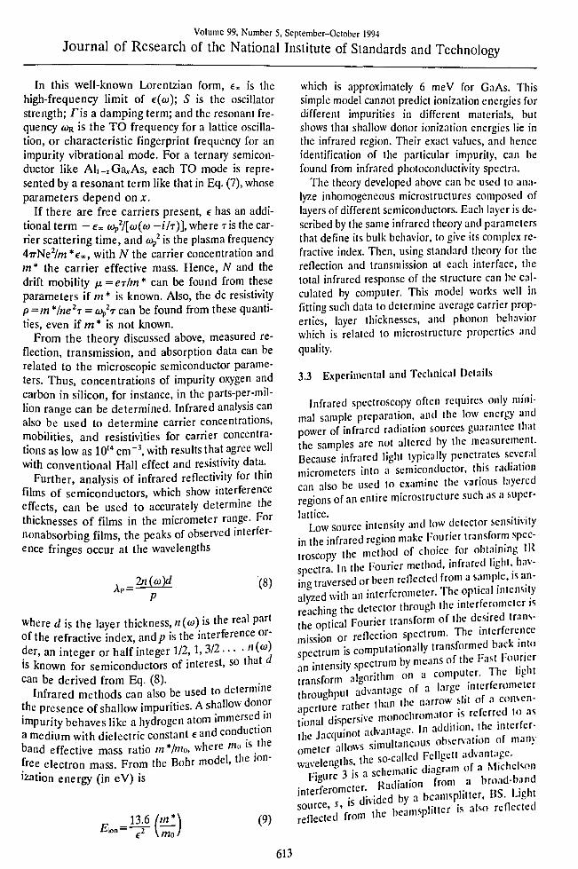
lattice Low source intensity and low detector sensitivity
in the infrared region make Fourier transform spec- troscopy the method of choice for obtaining IR spectra In the Fourier method infrared light hav- ing traversed or been reflected from a sample is an- alyzed with an interferometer The optical intensity reaching the detector through the interferometer is S optical Fourier transform of the desired trans- misZ or reflection spectrum The interference trum is computationally transformed back into rintensity spectrum by means of the I-ast lourcr ra so m Algorithm on a computer The light rouRhl advantage of a large interferometer
per ue rather than the narrow slit c^ a conven- tional dispersive monochromator is referred to as he cqlot advantage In addition he mterfer-
^^^rV^-^c2gamofaMichcson bdquor Ridiation from a broad-band inerferome e Rad-a-o ^ ^^ j^
-SSdt^o thf blsplitter is also reHected
613
Volume 99 Number 5 September-October 1994
Journal of Research of the National Institute of Standards and Technology
from fixed mirror Ml whereas light transmitted through the beamsplitter is reflected from a mov- able second mirror M2 The two light beams re- combine to produce a net intensity whose magnitude depends on the difference A between the paths that the two beams traverse As mirror M2 moves A varies continuously The intensity function (4) called the interferogram is
(^)=f 5()[l + cos(2Tr4)]d (10)
where S(f) is the intensity spectrum of the source as modified by the sample and=ajT7C is the opti- cal frequency in cm Equation (10) is the cosine Fourier transform of 5() which can be calculated from the inverse transform
5() = j^ [(l)-|(0)]cos(27rfd)d4 (11)
ng 3 Diagram of a Michelson interferometer configured for sample reflectance measurements S source BS beamspt bull Ml fixed mjrror M2 movable mirror which mov s as3 2 by he double-headed arrow SA sample D detector Th pc of source and beamsplitter depends on the region of the nr red
Mllnd MV deg I ^^ ^^^ - renec d from MI and M2 recombme to form the interferogram signal wH IS measured by the detector ^
This is implemented in the laboratory by process- ing the measured (I) with a computer to carry out the mverse transform The spectral resolution in wavenumbers of the Fourier system is 1L where L
is the total travel of the movable mirror Most ma- chines use a rapid scan method where the mirror is swept through its entire travel in a short time Many sweeps are averaged together to enhance the signal- to-noise ratio
Because of the small intensities of infrared sources especially at the very long wavelengths of the far infrared spectrum high-quality detectors are important Liquid helium bolometers give the highest sensitivity but are expensive and complex to operate Mercury-cadmium-telluride detectors op- erating at liquid nitrogen temperatures work well in the mid infrared spectrum Pyroelectric detectors operate at room temperature and are simple and rugged They are sufficiently sensitive from ultravi- olet to millimeter wavelengths for much semicon- ductor work
Commercial Fourier transform infrared systems are available that cover the near infrared to the far infrared spectrum by suitable choice of light source beam splitter and detector To avoid the effect of water vapor absorption on the desired spectrum these spectrometers are evacuated Often semiconductor samples must be cooled in order to better study electronic properties by removing the effects of lattice vibrations or phonons in the absorption spectra This can be accomplished to 77 K with liquid nitrogen and to 42 K with a liquid helium cryogenic system or by a mechanical refrigerator
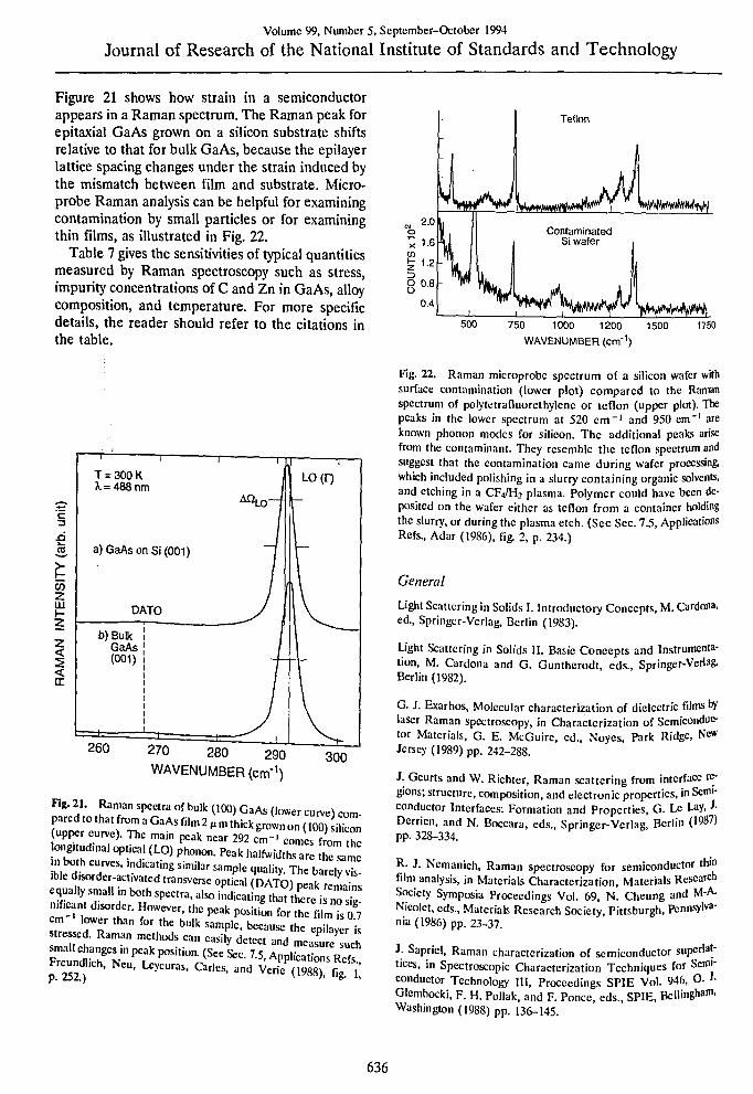
34 Illustrative Applications
Figure 4 illustrates the absorption peaks for in- terstitial oxygen at 1107 cm and substitutional carbon at 605 cm in Czochralski-grown silicon Such absorption data can be converted into oxygen concentration values giving a rapid nondestructive way to determine this important quantity Figure 5 demonstrates how a semiconductor film in this case an epitaxial layer of high-resistivity silicon de- posited on low-resistivity silicon gives clear inter- ference fringes that can be used to measure the layer thickness Figure 6 correlates resistivity ob- tained from infrared measurements with resistivity obtained from carrier transport measurements The data from epitaxial n- and p-type HgrCdi-xTe films are compared to results from conventional electrical measurements which require ohmic con- tacts that can be difficult to apply Figure 7 shows infrared reflectance data for an AlAs-GaAs super- lattice As the caption discusses in detail the TO phonon mode for each constituent material is clear as are interference fringes and other features The simple theory for infrared phonon response gives a
614
Volume 99 Number 5 September-October 1994
Journal of Research of the National Institute of Standards and Technology
1800 1600 1400 1200 1000 800 600 WAVENUMBER (cm
Fig 4 Infrared absorbance for a Czochralski-grown silicon wafer 2 mm thick derived from transmission spectra using a commercial Fourier spectrometer with a mercury-cadmium- telluride detector The characteristic interstitial oxygen Ime at 1107 cm- and the substitutional carbon line at 605 cm ap- pear Much of the remaining structure is due to silicon phonon modes The absorbance at 1107 cm is linearly related to the oxygen concentration Calibration data exist to convert ab- sorbance into oxygen concentration in parts per million atomic or atoms per cubic centimeter (See Sec 35 Applications Refs Krishnan Stout and Watanabe in Practical Fourier Transform Infrared Spectroscopy J R Ferraro and K Krishnan Eds Aca- demic Press San Diego (1990) fig 5 p 298)
070 mdash ~^
065 Spm
060 ^ ai
2 055 h -- bdquo -
DC 050 O CO m 045
25im
040 90jjm
035 -
030 - 1 i 1 1600 1400 1200 1000 ^
WAVENUMBER (cm )
Fig S Infrared reflectance spectra from f^ ^^jfj^^ of low carrier concentration silicon epitaxial layers on^ fc^ ^^^^
centration silicon substrates showing ^ ^^^i jofdif- can be used to determine epitaxial layer thickness ^^ ^ ferent thickness produce different fringe spacings accor fe Eq (8) (See Sec 35 Applications Refs Knshna^a^^ Watanabe in Practical Fourier Transfo m Infrar ^ pl^^^ troscopy J R Ferraro and K Krishnan Eds Acau
San Diego (1990) fig 25 p 333)
fit which reproduces all the main features of the spectra and allows an estimate of layer thickness
Table 4 gives the sensitivities of typical quantities measured by infrared spectroscopy such as intersti- tial oxygen concentrations in Si and GaAs substitu- tional carbon concentrations in Si and GaAs and B P and As concentrations in Si For more specific details the reader should refer to the citations given in the table
1
g[2 -pg 01
gt lU
T 1 I I llll| 1 1 I M I 11] I i Mil
bull Full FIR spectral fit - 300 Kj + Fj( using only first minimum
77 K Full FIR spectral fit
001 r
0001 0001 001 01
RESISTIVITY (0 cm) FROM HALL-EFFECT MEASUREMENTS
Fi2 6 Infrared values for dc resistivity omprcd ti tcsisiivily
values of 02 to 04 X^^ ^ ^^^^ dcvcd Resistivity values marked Full FIK spectral f m f^Is to the full far infrared (FIR) spectrum ltncr the um n cm t 2 0 cm - using the theory developed in hs laquo-clKn
20cm to 2ucm bull ^ f minimum raquocrc
r^^laquo^^lt^^^- results The I ^|bdquorjbdquo| mclbm) rciungtlttrade
35 References
General nclInrxhcoty Fourier Transform SplaquoulaquorgtAlaquo
Lic Press New York (972)
bdquo i7 bullbdquo D 11 Tanner Far infratcd ptT-
^ ^K B^wn c Acacmc Press Nc Yoik Waves Vol I (19S5) PP- 171-2f3
615
Volume 99 Number 5 September-October 1994
Journal of Research of the National Institute of Standards and Technology
E D Palik and R T Holm Optical characterization of semicon- ductors in Nondestructive Evaluation of Semiconductor Materi- als and Devices J N Zemel ed Plenum New York (1979) pp 315-345
S Perkowitz Submillimeter solid state physics in Infrared and Millimeter Waves Vol 8 K J Button ed Academic Press New York (1983) pp 71-125
10
gt- 08
^ 06 O y 04 Ul CC 02
0 10
I -
llaquo - 1 T
(a)
bullj bull
bull A - bullJ bull ri
5-mdashi^ bull bull
bull y -k]
1 1 r^-
250 300 350 400 450 WAVENUMBER(cm-)
Fig 7 Infrared reflectivity spectra for an AlAs-GaAs superlat- nce wh50 layer pairs Panels (a) and (b) show the same data points The peaks at 275 cm and 365 cm are the GaAs TO mode and AlAs TO mode respectively The peak at 290 cm- and shoulder at 355 cm- are interference fringes The minima m he spectra he a the positions of the structures longitud na opfcaphonon modes which are sensitive to layer thickness In
GaM ^ d luf r ^ deg-deg parameter^ G Asand AlAs and he growers nominal layer thickness AiA dcA-10 nm The improved fit in Panel (b) uses the same phonon parameters but allowed each layer thickness to
ct al gave d^^ - (75 plusmn 02) nm and ltGA = (82 plusmn 0 2) nm in
Applications
P M Amirtharaj G Holah and S Perkowit F-r inf troscopic study of In Ga As P Ph D ^ P (1980) -^^P-rPhys Rev 8 215656-5661
G J Brown and W C Mitchel Mid-infrared spectral response of semi-insulating GaAs in Impurities Defects and Diffusion in Semiconductors Bulk and Layered Structures Materials Re- search Society Symposia Proceedings Vol 163 D J Wolford J Bcrnholc and E E Haller cds Materials Research Society Pittsburgh Pennsylvania (1989) pp 157-162
J P Fillard M Castagne J Bonnafe and J Gall Scattering and absorption of infrared light on EL2 clusters in GaAs semi-insu- lating materials in Materials Characterization Materials Re- search Society Symposia Proceedings Vol 69 N Cheung and M-A Nicolet eds Materials Research Society Pittsburgh Pennsylvania (1986) pp 231-236
D K Gaskill J Davis R S Sillmon and M N Sydor Non- destructive characterization of carrier concentration and thick- ness uniformity for semiconductors using infrared reflectance spectroscopy in Modern Optical Characterization Techniques for Semiconductors and Semiconductor Devices Proceedings SPIE Vol 794 O H Glembocki F H Pollak and J i Soong eds SPIE Bellingham Washington (1987) pp 231-241
J Geist Infrared absorption cross section of arsenic in silicon in the impurity band region of concentration Appl Optics 28 1193-1199 (1988)
C E Jones T N Cassclman J P Faurie S Perkowitz and J Schulman Infrared properties and bandgaps of HgTeCdTe su- perlattices Appl Phys Lett 47 140-142 (1985)
C E Jones M E Boyd W H Konkel S Perkowitz and R Braunstein Noncontact electrical characterization of epitaxial HgCdTe J Vac Sci Technol A4 2056-2060 (1986)
K Krishnan Precise and Rapid Measurement of Interstitial Oxygen Concentration in Silicon Bio-Rad Semiconductor Notes No 102 Bio-Rad Semiconductor Measurement Systems 237 Putnam Ave Cambridge MA 02139 April 1983
K Krishnan A study of the spatial distribution of the oxygen content in silicon wafers using an infrared transmission micro- scope Bio-Rad Semiconductor Notes No 105 Bio-Rad Semi- conductor Measurement Systems 237 Putnam Ave Cambridge MA 02139 January 1985
K Krishnan and R B Mundhe Characterization of semicon- ducting silicon using FT-IR spectroscopy in Spectroscopic Char- acterization Techniques for Semiconductor Technology Pro- ceedings SPIE Vol 452 F H Pollak and R S Bauer eds SPIE Bellingham Washington (1983) pp 71-78
K Krishnan P J Stout and M Watanabc Characterization of semiconductor silicon using Fourier transform infrared spcc- tromctry in Practical Fourier Transform Infrared Spectroscopy J R Ferraro and K Krishnan eds Academic Press San Dicgo (1990) pp 285-349
B Lou S Perkowitz and R Sudharsanan Anisotropy = frared response of the AlAs-GaAs superlattice Phys Rev B 38 2212-2214 (1988) [Erratum Phys Rev B 39 1387 (1989)]
E Mcrk J Heyman and E E Haller Infrared absorption study of zinc-doped silicon in Impurities Defects and Diffusion m Semiconductors Bulk and Layered Structures Volume 163 Ma- terials Research Society Symposia Proceedings D J Wolford bull Bcrnholc and E E Haller cds Materials Research Society Pittsburgh Pennsylvania (1989) pp 15-20
616
Volume 99 Number 5 September-October 1994
Journal of Research of the National Institute of Standards and Technology
W J Moore Infrared transmission characterization of p-type gallium arsenide in Optical Characterization Techniques for Semiconductor Technology Proceedings SPIE Vol 276 D E Aspnes S So and R F Potter eds SPIE Bellingham Wash- ington (1981) pp 101-103
R C Newman Localized vibrational mode spectroscopy of im- purities in semiconductor crystals in Growth and Characteriza- tion of Semiconductors RA Stradling and PC Klipstein eds Adam Hilger Bristol (1990) pp 105-118
S Perkowitz and J Breecher Characterization of GaAs by far infrared reflectivity Infrared Phys 13 321-326 (1973)
S Perkowitz Far infrared characterization of HgCdi-Te and related electronic materials J Electronic Materials 14 551-562 (1985)
S Perkowitz D Rajavel I K Sou J Reno J P Faurie C E Jones T Casselman K A Harris J W Cook and J R Schet- zina Far infrared study of alloying in HgTe-CdTe superlattices Appl Phys Lett 49 806-809 (1986)
S Perkowitz Far infrared spectroscopy of HgCdi-Te and re- lated materials in Far-Infrared Science and Technology Pro- ceedings SPIE Vol 666 J R Izatt ed SPIE Bellingham Washington (1986) pp 120-125
S Perkowitz R Sudharsanan and S S Yom Far infrared anal- ysis of alloy structure in HgTe-CdTe superlattices J Vac Sci
Technol AS 3157-3160 (1987)
S Perkowitz R Sudharsanan S S Yom and T J Drummond AlAs phonon parameters and hcterostructure characterization
Solid State Commun 62 645-647 (1987)
B Senitzky and S P Weeks Infrared reflectance spectra of thin- epitaxial silicon layers in Optical Characterization Tlaquohmqucs for Semiconductor Technology Proceedings SPIE Vol 276 U E Aspnes S So and R F Potter eds SPIE Belhngham
Washington (1981) pp 222-226
R Sudharsanan S Perkowitz S S Yom and T J Drummond Far infrared reflectance spectroscopy of AlAs-GaAs mi- crostructures in Modern Optical Characterization Techniques for Semiconductors and Semiconductor Devices Proceedings SPIE Vol 794 O H Glembocki F H Pollak and J J Soong eds SPIE Bellingham Washington (1987) pp 197-201
R Sudharsanan S Perkowitz B Lou T J Drummond and B L Doyle Far-infrared characterization of AlAs-GaAs supcNat- tice structure Superlattices and Microstructurcs 4 OD
(1988)
L E Taroff C J Miner and A J Springthorpe ^P^lf]^^^ thickness measurements by reflection spectroscopy J- tit
Materials 18 361-367 (1989)
W M Theis C W Litton and K K Bajaj ^^^l^^f^lf mode spectroscopy of carbon-implanted GaAs in up acterization Techniques for Semiconductor TcchnologyJ^ro
cecdings SPIE Vol 276 D E Aspnes S So and K ed SPIE Bellingham Washington (1981) pp- i^
J Vindevoghel M Vindevoghel and Y Ixroy Ml[2bdquof far infrared conductivity for p-Si Evidence for inerband
tons Infrared Phys 18 99-105 (1978)
J M Zavada H A Jcnkinson and T J Gavanis Optical prop- erties of proton implanted n-typc GaAs in Optical Charactcriia- tion Techniques for Semiconductor Technology Proceedings SPIE Vol 276 D E Aspnes S So and R F Pollcr eds SPIE Bellingham Washington (1981) pp 104-108
4 Optical Microscopy
41 Introduction
In applications where the dimensions of interest are below the optical diffraction limit (-08 (im) electron microscopy is used by necessity However traditional optical methods remain useful for a large number of applications such as examining lo- pological features larger than -10 p-m examining defects or counting etchpits Several specialised forms of optical microscopy are highly valuable Nomarski scanning laser and microspcctropholo- metry In Nomarski microscopy interference meth- ods are used to incrcase the contrast between small differences in the surface level of a semiconductor wafer Scanning microscopy in both the visible and infrared spectral ranges allows two-dimensional imaging of features in a layer or structure I-inally microspectrophotometry allows film thickness determination from spectral analysis of reflected
^Scanning microscopy is also used in both Ihc visible and the infrared spectral ranges to form two- dimensional images of inhomogencitics in a semi- conductor The form called confocal micros- copy produces three-dimensional images [1] One visible light-scanning technique of special interest is the optical-beam-induced current method (abbrevi- ated OBIC or sometimes LBIC for laser-beam- induced current) which detects grain boundaries dislocations and other defects in semiconductors and semico doctor devices OBIC images rcprese-it patiTdistribulions of electrically active dcfecs ha nclude inclusions strain damage precipia cs a k^g faults twin boundaries dsloc-tnn c us-
--^ ^ts^dtsrrrd^c rerSofri-d the induced current b we n wo remote contacts on the sample s mca- ^s a function c^eser beam r^^^^
H n on t e^ rea of the sample which is hnmopc- nd defect-free does not generate any in- TZ curren nfrared scanning has been ued o ducedcurren n ^^^^^^ ^ ^^^^^
617
Volume 99 Number 5 September-October 1994
Journal of Research of the National Institute of Standards and Technology
Table 4 Infrared sensitivity Given are sensitivities for the measurement of interstitial oxygen [Oi] substitutional carbon [Cs] and nitrogen [Si-N-Si] in crystalline Si and substitutional carbon [CGJ and interstitial oxygen [Oi] in crystalline GaAs Also given are sen- sitivities for measurement of compositions jr of ALGai-As and HgCdi-Te and for carrier concentrations Na in Si and GaAs The sensitivity of far infrared low-temperature absorption measurements for substitutional boron [B] phosphorus [Ps] and arsenic [As] are also given The notations used for the measured quantity column are absorption coefficients a at subscripted wavelength in cm eg aiio7 absorption coefficient full width product aA at subscripted wavelength eg aAgu LO phonon frequency WLO plasma resonance frequency agtp transmission T and frequency ltigt
Method Matrix Quantity Measured Conversion Scnsitivity Ref quantity (see below)
LVM Si [0] 01107 300K
[Oi] = ax303plusmn002xl0cm-^ plusmn2x10^ cm- 1
LVM Si [Oi] otiim
300K [Oi] = ax314xl0cm-^ plusmn2x10 cm- 2
LVM Si [C] alaquoB 300K
[Cs]=axllxl0cm-^ plusmn2x10 cm- 3
Absorption Si [Si-N-Si] laquo3 300K
[N0 = aXl3xl0cm- = plusmn2x10 cm- 4
LVM GaAs [CcJ 77K
[Q] = azlxLlXlOcm- [Cs] = azlx8plusmn2x]0cm-
plusmn2xl0cm- 5 6
LVM GaAs [Oi] 10K
[C]=a4x8xl0cm- plusmn2x10 cm- 7
Phonon frequency
AIGa-As X oiLo or ftgti-o (wLo2T7ic)cm = 300K 2924 + 708C-26ampr^-4L13A3 8
IR cut off HgCd-Te X Ts 01 Ref 9 9
IR plasma frequency
Si N (Op 300K
(Op- = 4TrN^e-leurom 10
IR plasma frequency
GaAs N 6)p 300K
oip- = 4TrN^e-em 11
Absorption Si [B] a432i) 12K
[Bs] = axllxl0cm-- plusmn15x10-cm- 12
Absorption Si [P] 4316 12K
[Ps] = aXllxlOcm-2 plusmn15x10^ cm- 12
Absorption
CnlciiITtpH n-
Si [AsO 12K
[As] = axllxl0cm-- plusmn15x10-cm- 12
References
m A BaSldi wMBiiircc^ v1 ^^ deg= ^- ^-^e J Elecrochem Soc 132 1707 (1985) trochem So^Ue 2015 1989V AStrade ^i^^ bull ^ ^- ^^ ^i- bull Stallhofer and M Watanabe J Elec- (1991) ^ ^ ^^trade ^^^ S8 Annual Book of ASTM Standards 1005 (ASTM Philadelphia PA
[3] R C Newman and J B Willis J Phys Chem Solids 26 373 (1965) HJ H J Stem Anpl Phvs Lett 47 n-tQ nosl^ -u bull ^^^bullgt)- [5] A T Hunter H Kimura J P B kus H V Vf ^deg^ ^^ ^^^ =^ ^- A^ Appl Phys Lett 47 488 (1985) [6] M R Brozel E J Foulkes R W S i aid DT H deg- bull ^ ^^P^- ^y ^- ^^^^ (7] M Skowronski S T Neild and R E l^bdquo -o ^PP P^ys- Lett 49 337 (1986) 18] O K Kim and W G Spize J Appl ^hvT n f ^^l - ^^ d^D- [9] ^ Pinkman and V Nem^L^ X^yf ^1 L^)^ -- ^ ^PP- ^^y^- - ^1 (1985)
S C BH Tt^^ ^ ^=^-^^-- Soc 12482 (197) 112] S C Babcr Thin Solid Films 72 201 (1980)
618
Volume 99 Number 5 September-October 1994
Journal of Research of the National Institute of Standards and Technology
42 Physical Basis 421 Nomarsld Microscopy In Nomarski mi-
croscopy two microscopic images of a surface are formed so that they are slightly displaced in space and of opposite phase Interference bands appear where the images overlap The physical displace- ment and the interference bands heighten the visi- bility of small variations in surface levels
422 Scanning Microscopy In scanning mi- croscopy a spot of light whose size is limited by dif- fraction is scanned over a specimen The image of the specimen is developed point by point in sequen- tial fashion to be displayed or stored for analysis If the specimen is broadly illuminated and scanned in a raster pattern by a point detector (or raster scanned by a point source with the light sensed by a broad area detector) a two-dimensional image re- sults In the variation known as confocal scanning the specimen is illuminated in only a small region at any one time and a point detector senses light only from that same region This makes it possible to de- velop a three-dimensional image Confocal scan- ning also enhances resolution
The light can be sensed by any of several conven- tional detectors In the OBIC method however the detector is an external circuit that measures the cur- rent produced locally by the incident light Light m- tensity from a laser of even modest power creates a high density of carriers in the sample due to elec- tron-hole excitation The electrons and holes are af- fected by the electric fields associated with macroscopic defects such as grain boundaries m polycrystalline silicon so that the motion of the electrons and holes induces a current which is sensed by an external circuit Hence OBIC images clearly show the presence of defects and map out their locations
423 Microspectrophotometry Reflection spec- trophotometiy depends on the interference pattern caused by reflections from top and bottom surtaces of a transparent film The equations governing re_ flection from stratified dielectric media are denveu in most optics texts [2] Microspectrophotometiy i normally used for determining the film thCkness u a single layer on a substrate or the film thicknes es in a relatively simple multilayer stack As in en P sometry values of the functions 2(laquo) and ciw each of the layers of interest are needed to deter- mine the thicknesses The advantages ot rei tometry relative to ellipsometiy are that mo^t ot tn information is carried in the wavelength depe dences and it is relatively simple to focus the be down to spot sizes on the order of micrometers pj-
43 Experimental and Technical Details 431 Nomarski microscopy In Nomarski mi-
croscopy two microscopic images of a surface arc formed by a Wollaston prism The prism is placed between the eyepiece and the objective of the mi- croscope as shown in Fig 8
Eyepiece
Image I -
Analyzer
Image II
[-gt^ gt-V
Wollaston prism
Objective
y^^^^i Specimen
r-bdquo 8 Schematic diagram of a Nomarski interference miao-
plane of the paper (gtce yi
Modin (1973) fig 317 p I-^)
T bull h tr-tversinc the prism is divided into two Light t aversng mt ^^^^^^ ^^j
bration of the prism wii ^^ ^^^
angles to the Po^- ^^ ^in h sc Mcncc in- same inensty bt80 ^P ^^ P ^^^^p terference bands f ^J^ ^ displnccmcnl of These fringes 7^t ions The edges of he images magnify surface ^^^^^^ ^^^ ^^^
found
619
Volume 99 Number 5 September-October 1994
Journal of Research of the National Institute of Standards and Technology
432 Scanning Microscopy Figure 9 shows the main components of a scanning microscope It includes a light source usually a laser a scanning system which either moves the laser beam across a fixed sample or moves the sample relative to a fixed optical system optical elements to focus and ma- nipulate the beam and a detector The type of de- tector used depends on the scanning and imaging methods and on the wavelengths it may be a single photomultiplier tube or a detector array In the OBIC method it is an external circuit that mea- sures the photocurrent
Objective Collector
^^^-TKpbiect^^^-^^
Laser --^ If ^^ Detector
J ^
^
Display
xandy scannina
_ ^
Fig 9 Schematic diagram siiowing the main elements of a scanning microscope (See Sec 45 General Refs Wilson and Sheppard (1984) fig 11 p 2)
As stated above in some systems the light beam is scanned across a fixed sample This allows rapid acquisition and display of images however there are complications in designing the movable optical system and in maintaining good image quality In other designs the light beam is fixed and the sam- ple is moved to produce the raster pattern Although these systems are relatively slow the opti- cal design is simple and produces images of high quality
The OBIC technique (a typical experimental ar- rangement is illustrated in Fig 10) is one of the most important for semiconductor materials and devices and can readily be implemented with small lasers as sources A 1 mW HeNe laser produces 3 X 10 photons per second Based on a calculation using typical parameters for electron-hole genera- tion in a semiconductor this intensity is enough to generate a large density of electron-hole pairs about 10 cm~^ The electric fields associated with defects or doped regions separate the electron and hole in each pair These separated carriers can in- duce a current by flowing through an appropriate external circuit (Depending on whether the sample includes a p-n junction or not and on the nature of the circuit either photovoltages or photocurrents can be measured)
Neutral Density Filter Wheel
Beam expander
Beam splitter
Beam splitter
Acousto Optic Modulator
Laser HeNe 115 urn
Host Computer and
Image Display A0 converters AOM control x-y stage control z stage control NDF control Laser control
X y stage
Sec 4 5 renri D I Caser-beam-mduccd current) (See ^ec 45 General Refs Moore Hennessy Bajaj and Tennant (1988)
620
Volume 99 Number 5 September-October 1994
Journal of Research of the National Institute of Standards and Technology
Scanning methods can be used equally well in the visible and in the infrared regions In one typical in- frared system the source is a semiconductor laser operating at 13 jim wavelength (giving a spot di- ameter of about 2 |xm) with detection accom- plished by germanium photodiodes The sample is mechanically moved to produce raster scanning and the resulting images are taken at resolutions of 512 pixels by 512 pixels
433 Microspectrophotometry Interference of light waves reflected from each interface of a multi- layer film structure determines the reflectance of the structure The reflectance spectrum depends on angle of incidence of the radiation the refractive in- dices of the media polarization of the radiation and film thicknesses [4] Whereas the same equa- tions describing reflection and transmission apply m both ellipsometry and reflectance spectrophotome- try the problem is somewhat simplified in the case of reflectometry where polarization is usually ig- nored Normally the reflected light intensity is recorded versus wavelength Then the thicknesses are calculated by fitting measured spectra to calcu- lated spectra based on a model of the layer struc- ture and known dielectric constants Measurements can also be made of the reflectance versus polariza- tion angle or versus angle of incidence but this is not normally done in microscopic measurements because these parameters are difficult to change systematically within the microscope environment The most frequent application of microspectropho- tometry is the determination of thicknesses of sim- ple dielectric stacks on a substrate but micro- spectrophotometry can also be used like ellipsome- try to find the dielectric function of film layers and hence film layer composition [4] Because of the re- laxed constraint on the angle of incidence and tne relative speed of processing data microspectropho- tometry is an ideal way to map the uniformity or
wafer film thickness
44 Illustrative Applications
Figure 11 shows the power of OBIC imaging to detect flaws in semiconductor materials su^h ^s^^ icon even when the material is incorporated in an operating device such as a transistor Figure iz shows an infrared scanning system ^J^P^J^ oxide particles embedded in Czochralski-grown silicon even displaying those partcle^sm^ehan the infrared beam diameter of 2 ^tm By focusing different depths in the sample it ^ P^^^^ J obtain some depth-dependent information as well
Fig 11 An OBIC image formed by monitoring the cmillcr- base current in a silicon transistor while a laser beam is scanned across the transistor The dark straight lines arc lines of disloca- tions in the silicon (Sec Sec 45 General Rcflaquo Wilwn and Sheppard (1984) fig 16 p 8)
45 References
[1]
[2]
[3]
[4]
G O Ziao T R Cbrle and G S Kino Real-lime confiWil scanning optical microscope Appl Phyraquo Utt 53 716
M^Born and E Wolf Principles of Optics Pcrpiwin Prcraquo New York (1975) p 61 P Burggraf How thick are your thin films Semiconductor
International (1988) p 96 rlm on S E Slokiwski Measuring refracKve mdKXS of films on semiconductors by microreneCometry in Integrand Circuit Metrology Inspection and Process lt^^-J SedingrSPIE W H Arnold ed SPIE Bclmgham Washington (1990) p 253
General
of Physics Adam Hilgcr Bnsiol (1981)
Sr~il-raquoi - ^ - bull ^ ^
Hilger Bristol (1985)
621
Volume 99 Number 5 September-October 1994
Journal of Research of the National Institute of Standards and Technology
rraquo 12 Infrared scanning microscope images of oxide particles n heat-treated (100) Czochralski silicon The microscope usel semiconductor laser emitting at 13 ^m to give a spot s^ze of -2 m Particles of this size or greater are directly imaged SmHer parties can still be seen although as spots 2 m acrol bee e the qrstem can detect intensity variations of about 05 The depth of focus s 30 ^m Panels (b) and (e) show successively deeper probes into the sample relative to Panel (a) The3 planeis 60 m deeper in Panel (b and 120 m deeper in pl^ c The sets of oxide images marked a Ir and cabdquo 1^
followed m and out of fcKus through the panels (See Sec 4 5 Appicatictrade Refs Laczik Booker Faser and Shaw 98^ ]
Microscopy of Semiconducting Materials Institute of Physics Conference Proc 117 A G Cullis and N J Long eds Institute of Physics Bristol (1991)
S Hildebrandt and W Hergert Unified theoretical description of the CL EBIC PL and EBIC contrast profile area of an indi- vidual surface-parallel dislocation Phys Stat Sol (a) 119 689- 699 (1990)
R Kcclcr Confocal microscopes RampD Magazine (April 1991) pp 40-42
H Modin and S Modin Metallurgical Microscopy John Wiley New York (1973)
bdquoii
T Wilson and C Sheppard Theory and Practice of Scanning Optical Microscopy Academic Press London (1984)
Applications
J Bajaj L O Bubulac P R Newman and W Tennant Spatial characterization of semiconductors using laser beam induced current (LBIC) in Modern Optical Characterization Techniques for Semiconductors and Semiconductor Devices Proceedings SPIE Vol 794 O J Glembocki F H Pollak and J J Song eds SPIE Bcliiiigham Washington (1987) pp 136-141
J Bijij W E Tennant and P R Newman Laser beam induced current imaging of surface nonuniformity at the HgCdTcZnS interface J Vac Sci Technol A 6 2757 (1988)
S Haq G Hobson K E Singer W S Truscott and J O Williams A transmission electron microscopy investigation of GaAS]-)Sb)-GaAs superlattices grown by molecular beam epi- taxy in Microscopy of Semiconducting Materials Institute of Physics Conference Proc 100 A G Cullis and J L Hutchinson eds Adam Hilgcr Bristol (1989) pp 337-341
P Kidd G R Booker and D J Stirland 3-D distribution of inhomogeneitics in LEC GaAs using infra-red laser scanning mi- croscopy in Microscopy of Semiconducting Materials Institute of Physics Conference Proc 87 A G Cullis and P D Augustus eds Adam Hilger Bristol (1987) pp 275-280
Z Uczik G R Booker R Falster and N Shaw Investigation of precipitate particles in Si and CdTc ingot material using the scanning infrared-red microscope (SIRM) in Microscopy of Semiconducting Materials Institute of Physics Conference Proc 100 A G Cullis and J L Hutchinson eds Adam Hilgcr Bris- bullol (1989) pp 807-812 ^j^^bdquo^^ yp
Y-C Lu R K Route D Elwell and R S Fcigelson Etch pit studies in CdTe crystals J Vac Sci Technol A 3 264 (1985)
J- L Mariani B Pichaud F Minari and S Martinuzzi Direct iletermination of the recombination activity of dislocations in FZ silicon by LBIC measurements in Microscopy of Semiconduct- ing Materials Institute of Physics Conference Proc 100 A G- Cullis and J L Hutchinson eds Adam Hilgcr Bristol (1989) pp 801-806
C J L Moore J Hennessy J Bajaj and W E Tennant Find- ing faults in focal plane arrays Photonics Spectra (September bull988) pp 161-166
622
Volume 99 Number 5 September-October 1994
Journal of Research of the National Institute of Standards and Technology
M Ogura M Tajima and Y Tokumaru Scanning optical fiber microscope for high resolution laser beam induced current im- ages of semiconductor materials in Materials Characterization Materials Research Society Symposia Proceedings Vol 69 N Cheung and M-A Nicolet eds Materials Research Society Pittsburgh Pennsylvania (1986) pp 251-256
D J Stirland P Kidd G R Booker S Clark D T J Hurle M R Brozel and I Grant The behaviour of arsenic-rich defects in quenched semi-insulating GaAs in Microscopy of Semicon- ducting Materials Institute of Physics Conference Proc 100 A G Cullis and J L Hutchinson eds Adam Hilger Bristol (1989) pp 373-378
5 Modulation Spectroscopy
51 Introduction
Modulation spectroscopy is a sensitive technique which can determine fine details of interband transitions in semiconductors In semiconductor superlattices and other microstructures detailed knowledge of the complex interband transitions can be used to characterize quantum well widths po- tential barrier heights and widths electric fields and the amount of strain in strain layer systems
52 Physical Basis
The principle behind modulation spectroscopy is that a periodic physical perturbation applied to a sample elicits the derivative of the samples optical response to that perturbation The derivative fea- ture amplifies weak features in the response func- tion and suppresses large constant background levels This gives modulation methods very high sensitivity to small spectral features that are invisi- ble in conventional spectroscopy
To illustrate the origin of the derivative response consider the reflectivity R of a sample This de- pends on the samples dielectric function which de- pends on many physical properties For example the dielectric function depends on an applied elec- tric field E hence R also depends on pound If the ap- plied electric field has a dc component Eo and a small ac component pound cosOt (0 is the modulation angular frequency) the reflectivity can be written as laquo(pound)=i(poundo + poundcos2r) If poundiltlt Eo this expres- sion can be expanded in a Taylor series where only the first two terms are kept that is
RE)^RiEo)+Ecosnt) (12)
The first term depends on E but not on time whereas the second term is a periodic function oi
time at the modulation frequency fi Hence the ac portion of the reflectance at frequency can be de- tected with a lock-in amplifier this signal is propor- tional to the derivative ddE Thus small structures in the optical spectrum of R(E) arc enhanced even with the sample at room tempera- ture A periodic perturbation can be applied to any physical property affecting the samples optical response Examples are elcctroreflcciance where a periodic electric field is applied to a sample while its reflectance spectrum is measured and pholore- flectance where optically injected carriers from a chopped laser beam modulate the built-in sur- face or internal electric fields thereby modulating the reflectance of the sample Other forms of mod- ulation spectroscopy have been reviewed by Aspncs [1] The following discussion concentrates on clec- troreflectance and photorcllectancc two forms of modulation spectroscopy currently in common usage Because photorcflcclance results from the modulation of built-in electric fields this discus- sion applies generally to either clcctrorcflcctance or photorellectance
The enhancement of spcclroscopic structures that appear at energies corresponding to energy gaps and other critical points in the joint density of states of the material under study is one useful re- sult of modulation methods The method becomes more useful still when the measured spectral line shapes can be connected to microscopic parameters through theory The relationship that makes this connection is [2]
R (13)
where dR is the change in reflectivity due to the ap- plied modulation M and Jo are the changes m The real and imaginary parts respectively of the complex dielectric function c = +o and a and ^ are called the Scraphin coefncents Near the cn- gap of a bulk sample^ = 0 however for cm
S microstructures where interference effect S cur both a and P need to be considered ad r ^U ind Jf must bolh be known llicsc cm eCctbed from general band hco^^ and from
S electric function theory In the case of elccrnrc- ditleciric bdquo_bdquorflcclancc different spectral
bdquolv e ire required dependine on Ihe aEr- enlanJi) esare eq bdquobdquodulalior licid is bdquogt edraquobdquobdquolbdquoee regime (2] hifh
i^ rstrk effec) inlermediae Held (Hani- poundfdScorlowWThehighedeaegt
623
Volume 99 Number 5 September-October 1994
Journal of Research of the National Institute of Standards and Technology
not usually studied under modulation conditions as a high electric field breaks down the normal selec- tion rules and results in a Stark shift of the band structure The analysis of spectra based on interme- diate and low field theories is discussed in reference to representative spectra in the illustrative applica- tions section below
53 Experimental and Technical Details
A modulation measurement requires a light source a monochromator and a detector as in con- ventional spectroscopy and a means to apply the modulation to the sample These elements are shown in Fig 13 The source can be an incandes- cent or discharge lamp Generally a monochroma- tor of 025 m focal length provides adequate energy resolution but higher resolution may be needed in some cases
Monochromator
gt
Variable gt neutral density
filter
Sample
^-A^^
Detector ^--xj ^ Filter
DC signal
ARR
copper J-LJ-Ln_0
Laser(or other l secondary light source)
rg 13 Diagram of a photoreHcctance spectrometer illustrat- ing lamp with followmg optics and electronics to obtain the spec-
^lCru T T ^ trade^ g- The variable neutral densbdquoy fUcr holds the constant part of the detected signal n depcnden of wave cngth facilitating evaluation of the ^atio of
The light reflected from the sample is detected by a photomultiplier tube or a photodiode It con- tains a steady (dc) component Rh (bdquo is the incident light intensity) and a periodically modulated (ac)
component ARIo To obtain ARR the dc signal and the ac signal must be separately measured and then a ratio of these signals is taken It is also possible to electronically hold the dc signal (corresponding to Rio) constant during the measurement This can be done by a feedback loop that changes the gain of the detector to keep its dc output constant or as shown in Fig 13 by mounting a circular continu- ously variable neutral density filter on a servo motor and inserting it before the sample
For photoreflectance light from a modulated op- tical source such as a laser whose photon energy ex- ceeds the samples energy gap impinges on the sample For electroreflectance of a doped semicon- ductor the varying electric field can be applied be- tween an ohmic contact on the samples back surface and a transparent gate electrode on the front of the sample 5 nm to 10 nm of deposited gold or aluminum is an adequate electrode A sec- ond method is to put the sample in an electrolyte such as a KCl solution or an acidic solution The resulting electric field at the sample surface can be changed by varying a voltage applied between the sample and a platinum counter electrode Photore- flectance and electroreflectance spectroscopy both provide highly detailed spectra even at room tem- perature so that sample cooling is usually not needed
54 Illustrative Applications
Figure 14a shows the sensitivity of modulation spectroscopy by comparing the reflectivity spec- trum of GaAs in the interband region to the much more detailed ARR spectrum obtained by elec- troreflectance Figure 14a is illustrative of the low field case Here the spectra near the energy gap can be fitted using [3]
AR -^=[e(ftw-pound+r)-] (14)
where w is the photon energy Eg is the gap energy 0 is the phase factor F is the lifetime broadening parameter and the quantity m takes on the values 2 25 and 3 for excitonic three-dimensional and two-dimensional critical points respectively Hence the critical point type and energy can be de- termined from fitting this line shape Aspnes [3] has also developed a three-point method for extract- ing critical point energies which for simple spectra eliminates the need for a full spectrum fit
Shown in Fig 14b [4] is the photoreflect- ance spectra of a moderately n-type doped
624
Volume 99 Number 5 September-October 1994
Journal of Research of the National Institute of Standards and Technology
Electroreflectance (300 K)
E ^deg Ea
0 1 2 3 4 5 6 ENERGY (eV)
Fig 14a Conventional interband reflectivity spectrum for GaAs at 300 K compared to the interband ARIR spectrum at 300 K obtained by electroreflectance The broad features in the plot for reflectivity R such as the shoulder at the gap energy poundbdquo be- come obvious sharp lines in the ARR data which lie on a base- line of zero signal Structure at Ebdquo + A which was invisible m the reflectivity spectrum is apparent in the ARR curve (Sec Sec 55 General Refs Pollack and Glembocki (1988) fig 1 P- 25)
identified by the presence of oscillatory behavior the so-called Franz-Keldysh oscillations at energies greater than the energy gap of the material Modulation intensities are usually greater for the high field case than for the low field case Materials information (eJectric fields and energy gap values) is typically extracted from Franz-Keldysh oscilla- tions using the Aspnes asymptotic approximation
[5]
xcos Hn^n gt where 0 I and poundg are defined above and MJ is the electro-optic parameter [C-pound--3277-M]- bull lt is the electron charge E is the dc electric field is Plancks constant and n is the reduced interband effective mass Since successive cxtrcma represent a change of TT in the argument of the cosine term in Eq 15 the energy of the lh cxtrcma [5] can IK
written as
15
10
^ 05
X
00
-05
-10
-15
mdashI r^
Intermediate Field 293 K
068 070 0-72 Energy (eV)
074 076
Fig 14b Photoreflcctance spectra for the ^J^^i^^^J^j case for a moderately doped sample of InGaAsInP wi extrema ( = 2 3)
(~ 1X10 cm) sample of Ino^GawyAs illst^^S the intermediate field line shape This case ca
V=0 + 3 2 litzEAT [ m J (16)
Hence the phase factor and electro-optic energy can e obtained from the intercept and slope of a f ifu-FA^ vs It is noteworthy that the
iScd from he clccroopic cncrffir rcurne
bdquohemacral Hence deer ^^^^^^ ^^^
nondesiruui ^^ y^bdquo_ ^^
S^XeSinaspace charge region
[6] through the Schot^equ^^^^^^^^^^
^bull^Tmctpp^di^ turn well 1 lie gt-iiin lttructurc to give
specira raquo fJbdquobdquoicraquolly filcJ 0 JCer- roVClSh aJ Al mole fraeion e
625
Volume 99 Number 5 September-October 1994
Journal of Research of the National Institute of Standards and Technology
155 160 165 ENERGY (eV)
Fig 15 Photorencctance spectra of GaAsAlGa_ As multi- ple quantum well (MOW) with nominal t value 024 and nomi- nal barrier and well thickness of 15 nm and 22 nm respectively Spectra (1) to (4) were measured at locations spaced 047 cm apart along a straight line In each the peak at 142 eV marked poundbdquo comes from the direct gap of the GaAs substrate the peak m rkcd A near 172 eV comes from the direct gap of the AlGa As barners and the remaining features marked bdquo and -l -123 ) between 143 and 168 eVcome from light and heavy hole nterband transitions characteristic of the MQW en ergy bands The AlGa As and features shift with spa^al
^lr 1 a dT4i 4raSTef V -
Table 5 presents the sensitivities to typical quan- mes measured by photorenectance spectroscopy such as composttton stress electric field strength surface photovoltage and doping density Forbore peafic detatls the reader shoufd refer to the cha
tions given in the table
55
[1]
References
D E Aspncs Modulation spectrosconvelrrtrlr f ^s on the dielectric functionof se^U f i Ha^d book on Semiconductors Vol 2 T lt ^-
Balkanski eds North-HoilandNcwU S) 109^
[2] B O Seraphin and N Bottka Franz-Keldysh effect of the refractive index in semiconductors Phys Rev 139 A560 (1965)
[3] D E Aspncs Third-derivative modulation spectroscopy with low-field elcctroreflectance Surface Science 37 418 (1973)
[4] J P Estrera W M Duncan Y C Kao H Y Liu and E A Beam Systematic optical and x-ray study of InGai-As on InP J Electronic Materials 20 983 (1991)
[5] D E Aspncs and A A Studna Schottky-barrier electrore- flectance application to GaAs Phys Rev B 74605 (1973)
[6] W M Duncan and A F Schrcincr Surface state study of ion implanted GaAs (Se) from photoreflectance Solid State Communications 31 457 (1979)
General
J 1 Pankove Optical Processes in Semiconductors Prentice Hall Englewood Cliffs (1971) pp 391-407
F H Pollak and O J Glcmbocki Modulation spectroscopy of semiconductor microstructurcs an overview in Spectroscopic Characterization Techniques for Semiconductor Technology III Proceedings SPIE Vol 946 O J Glcmbocki F H Pollak and F Ponce eds SPIE Bellingham Washington (1988) pp 2-35
Applications
P M Aminharaj J H Dinan J J Kennedy P R Boyd and 0 J Glcmbocki Photorenectance study of HgcvCdoaTe and CdZn-Tc E transition J Vac Sci Technol A42028 (1986)
R N Bhattacharya H Shen P Parayanthal and F H Pollak Elcctroreflectance and photoreflectance characterization of the space charge region in semiconductors ITOInP as a model sys- tem in Modern Optical Characterization Techniques for Semi- conductors and Semiconductor Devices Proceedings SPIE Vol 794 O H Glcmbocki F H Pollak and J J Soong eds SPIE Bellingham Washington (1987) pp 81-87
R C Bowman R L Alt and K W Brown Photoreflectance spectroscopy studies of alloy composition and ion implant dam- age in zincblcnde-type semiconductors in Modern Optical Char- acterization Techniques for Semiconductors and Semiconductor Devices Proceedings SPIE Vol 794 O H Glcmbocki F H Pollak and J J Soong eds SPIE Bellingham Washington (1987) pp 96-104
R C Bowman D N Jamieson and P M Adamson Optical and structural characterization of boron implanted GaAs in Spectroscopic Characterization Techniques for Semiconductor Technology III Proceedings SPIE Vol 946 O J Glcmbocki F H Pollak and F Ponce eds SPIE Bellingham Washington (1S88) pp 65-75
J P Estrera W M Duncan Y C Kao H Y Liu and E A- Beam Systematic optical and x-ray study of InGai -As on InP J Electronic Materials 20 983-987 (1991)
O J Glcmbocki Ellipsomctric-clectrolyte clcctro-rcflcctance study of the SiSiO interface in Spectroscopic Characterization Techniques for Semiconductor Technology Proceedings SPIE Vol 452 F H Pollak and R S Bauer eds SPIE Bellingham Washington (1983) pp 130-141
626
Volume 99 Number 5 September-October 1994
Journal of Research of the National Institute of Standards and Technology
O J Glembocki and B V Shanabrook Photoreflectance char- acterization of microstructures using a dye laser system in Mod- ern Optical Characterization Techniques for Semiconductors and Semiconductor Devices Proceedings SPIE Vol 794 O H Glembocki F H Pollak and J J Soong eds SPIE Bellingham Washington (1987) pp 74-80
R Glosser and N Bottka Comparative response of clcctrore- flectance and photoreflectance in GaAs in Modern Optical Characterization Techniques for Semiconductors and Semicon- ductor Devices Proceedings SPIE Vol 7940 H Glembocki F H Pollak and J J Soong eds SPIE Bellingham Washington (1987) pp 88-95
T K Gupta Effective bandgap shrinkage measurement in sili- con solar cell by electroreflectance method in Spectroscopic Characterization Techniques for Semiconductor Technology III Proceedings SPIE Vol 946 O J Glembocki F H Pollak and F Ponce eds SPIE Bellingham Washington (1988) pp 76-81
B K Janousek and R C Carscallen Approaches to enhancing the sensitivity of direct coupled photoacoustic spectroscopy as applied to GaAs in Spectroscopic Characterization Techniques for Semiconductor Technology Proceedings SPIE Vol 452 F H Pollak and R S Bauer eds SPIE Bellingham Washington (1987) pp 121-127
C E Jones M E Boyd W H Konkel S Perkowitz and R Braunstein Noncontact electrical characterization of epitaxial HgCdTe J Vac Sci Technol A 4 2056-2060 (1986)
Y R Lee A K Ramdas F A Chambers J M Meesc and L R Ram Mohan Piezomodulated electronic spectra of semicon- ductor heterostructurcs GaAsAlGaAs quantum well structures in Spectroscopic Characterization Techniques for Semiconduc- tor Technology Proceedings SPIE Vol 452 F H Pollak and R S Bauer eds SPIE Bellingham Washington (1987) pp 105- 110
T W Nee T L Cole A K Green M E Hills C K U)we-Ma and V Rehn Infrared-wavelength modulation spectra of In- GaAs grown by MBE and LPE in Spectroscopic Characteriza- tion Techniques for Semiconductor Technology Procccdmgs SPIE Vol 452 F H Pollak and R S Bauer eds SPIE Belling-
ham Washington (1987) pp 142-151
G Niquet J F Dufour G Chabrier M QJani and P Vernier Characterization by electroreflectance of thin films and thin liim interfaces in layered structures in Modern Optical Characteriza- tion Techniques for Semiconductors and Semiconductor Devices Proceedings SPIE Vol 794 O H Glembocki FH Pollak and J J Soong eds SPIE Bellingham Washington
(1987) pp 111-115
P- Parayanthal H Shen F H Pollak O J Gl^^bocki B V Shanabrook and W T Beard Photoreflectance of OaA GaAlAs multiple quantum wells topographical variations in D
rier height and well width Appl Phys Lett 48 U0gt- (1986)
U K Reddy G Ji R Houdre H Unlu D Huang and R Morkoc Study of 6aAsAIGaAs and InGaAsGaAs multiple
quantum wells grown on non-polar substrates by P tance in Modern Optical Characterization Techniques for scm
conductors and Semiconductor Devices Proceedings SPIE Vol 794 O H Glembocki R H Pollak and J J S(K)ng eds SPIE Bellingham Washington (1987) pp 116-120
H Shcn S H Pan F H Pollak and R N Sacks Pholorcflec- tance and thcrmoreflcctancc of a GaAsGaltiKAIiilaquoAs mulliplc quantum well in Spectroscopic Characterization Techniques for Semiconductor Technology III Proceedings SPIE Vol 946 O J Glembocki F H Pollak and F Ponce eds SPIE Dcllinghim Washington (1988) pp 36-42
H Shcn Z Hang F H Pollak K Capuder and P E Norris In silii monitoring of OMVPE of GaAs and GJI-AIJAS
(x = 017) by contactlcss photoreneclance in Surface and Inter- face Analysis of Microelectronic Materials Processing and Growth Proceedings SPIE Vol 1186 L J Brillson and V H Pollak eds SPIE Bellingham Washington (I9S9) pp 27-15
X Yin F H Pollak J T Filch C H Djorkman and O lucov- sky Photoreflectance study of strain at SiSiO inlcifaccs pre- pared by thermal oxidation of silicon in Surface and Inlcrfacc Analysis of Microelectronic Materials Processing and Griiwlh Proceedings SPIE Vol 1186 L J Drillson and V II Pollak eds SPIE Bellingham Washington (I9S9) pp 122-lm
6 Photoluminescence 61 Introduction
Photoluminescence (PL) depends on the fact that electrons residing in the valence band of a semicon- ductor can be excited via optical absorption to the conduction band to an impurity or to a defect level in the energy gap PL can be used to determine the energy gap of a semiconductor sample This tech- nique is especially useful for III-V and II-VI ternary
alloys like AlGa-As and ZnCdi-Tc because the energy gap which varies with the compostional parameter x must be accurately known for most ap- plications When this process is inverted x cari be found from the gap value and the X-^^ between gap energy and composlion Photolu- mine ence also deScts the presence of mpurtcs Tnd crystalline defects in semiconducors whch af- feet materials quality and device performance Lach ^ urily prod ces a characteristic feature or set of Hu s in the spectrum Hence the trnpunty type an be i entifieS and multiple impurtes can he
bull bull ibdquo pr tnccirum n some cases PL laquo r net So of impiis Co can measure IM CO ^^^^ ^ ^bdquo
LXani caloriraquoruraycobdquoccnbdquoiobdquo
Sfeconcraquoaiobdquoandcoilpelaquo-
62 Physical Basis bdquo rpltilis from radiative relax-
reteSlonlciraquoclaquonlnpoobdquocbdquocbdquo
627
Volume 99 Number 5 September-October 1994
Journal of Research of the National Institute of Standards and Technology
Table 5 Photoreflectance spectroscopy sensitivity Given are sensitivities for the measurement of crystallinity x stress Xt field strength Foc surface photovoltage Vi and doping density A^d- The notations used for the measured quantity column are intensity energy hv damping F bandgap Eg splitting energy Apoundspii deformation potential b compliances Sn and 5i2 energy of Franz Keldysh oscillation lobe poundbdquo oscillation number m energy difference pound2-^1 shift of critical point SEcp and spacing of Franz Keldysh oscillations ApoundFKO- AK is the built-in potential minus the photovoltage of the laser minus the thermal energy
Method Matrix Quantity Measured quantity
Conversion Sensitivity Ref (see below)
PR Si crystallinity IJivr qualitative 1
PR In^Gai-iAs X E poundgeV= 1425 - 1337r+027QJ- r = 0to015 2
PR GaAsGaAlAs field strength Ebdquo vsm 77177= 0 +(43)[(poundbdquo -poundo)lOf= pounddlt-(2to4)x 4 lO Vcm
PR metalGaAs surface photovoltage
Ebdquo vs m m7r=0 + (43)[(poundbdquo -Ebdquo)liOY- K-= (073 plusmn 002) V 5
PR GaAs doping density E2-E
(pound2-pound)(346xl0^)cm
Nd = (lxlOto lxlO)cm-^ 6
PR GaAs doping density 5poundcp SpoundcpSiVa = (58plusmn05)xlO-^cVcm^
NdgtlxlOcm- ^
PR GaAs doping density ApoundFKO ApoundFKO = const xAfj Ad = (6xl0to 8
bullr-t --
3x10) cm-
References
m B fZ^T ^-degdeg= K- Joyner and G Pollack J Electronic Mat 20 949 (1991) 2 R E Naho-y M^A Pollack and J C DeWinter J Appl Phys 46 775 (1975)
tzZdegtVJjZTS^ deg=deg8t^ deg- bull deg^^ ^ ^- C^-^^ gtbull Appl Phys 67 4389 (1990) T Kanata H [4] X vTn F H Pollak 1 x l-^T^^^ ^ ^^ T ^^hino Phys Rev B41 2936 (1990)
WrS R W K 1 ski enHtTw^i ^f ^^ ^ ^P^ P^^^ L=laquo- ^lt 1278 (1990 N Bottka D K Gaskill P D [51 X Yin H M rh p u I ^ ^ bullbull ^y^^ degtradeh 107 893 (1991)
260 (Tw) bull deg ^- ^^ ^- ^- ^deg=trade- P- D- Ki^chner G D Pettit and J M Woodall Appl Phys Lett 58
m U PS t Prruf^LTKapiLand W- U^--I^ ^^- - ^^^ ^^^^ m W M Duncan and A FLSSSsTatrcr^ 3^4577^^79
628
Volume 99 Number 5 September-October 1994
Journal of Research of the National Institute of Standards and Technology
must equal or exceed the energy difference between the initial and final states of the electron Such an excited electron usually returns to its initial state af- ter a short time If the excited electron returns to its initial state by radiative means the process emits a photon whose energy is the difference between the excited and the initial state energies The spectral distribution of the emitted photons shows an emis- sion peak at the energy (or wavelength) corre- sponding to each excited level
Photoluminescence is complicated by the behav- ior of the electron during its excited period The ex- cited electron leaves behind it a deficiency in the valence band a mobile hole The Coulomb attrac- tion between the excited electron and the hole can bind the two particles into a system called a free ex- citon much as a proton and an electron form a bound hydrogen atom The exciton can move as a unit through the crystal but carries no current be- cause its net charge is zero From this perspective the return of the electron to its initial state can be viewed as the collapse of the temporary excitonic state when the electron recombines with the hole
The exciton influences the PL spectrum in sev- eral ways Because it is a bound state the excited state energy is slightly less than the bandgap energy generally by a few meV Hence for PL near the en- ergy gap the equation for the energy of the emitted photon is
^(0=EtmdashEc (17)
where poundraquo is the binding energy of the excitonic state This equation applies for a direct energy gap semiconductor For an indirect gap semiconductor a phonon must also be involved to properly con- serve momentum Then the equation for the einit- ted photon energy is (poundph is the photon energy)
fi(o=Eg-Etn-Ef ^
However this free exciton recombination domi- nates only when the sample is very pure When donor acceptor or neutral impurities are preseni free excitons respond to the Coloumb fields of these defects to form bound excitons Each type or ext ton produces a PL peak when recombination oc- curs and each can be identified in the spectrum
6J Experimental and Technical Details
Figure 16 shows the main elements of a slandard PL arrangement Any of several commerciaUy avail able types of laser may be used provided that
energy of the lasers photons exceeds the energy gap of the material and the laser power is adequate to excite a usable PL signal An argon ion laser is suitable for many semiconductors of technological interest such as Si (112 eV) AIGai-xAs (142 eV to 216 eV) and Zn^Cdi-iTe Laser powers lt50 mW are usually adequate but power densities must be minimized to avoid sample healing effects It is generally possible to avoid heating and still ob- tain adequate signal to noise by defocusing the laser or reducing the incident laser power
(5ltr([^fe Grating monochromator
Sample in cryostat
FiE 16 Schematic diagram of a photoluminescence arrange- ment showing the exciting Ar or Kr laser filter F2 to bllt^ unwanted laser lines the sample mounted n a c^ostal lens L2 to bring the PL radiation to the mmochromator entrance slit chopping wheel Cl to modulate the light for IKk-in detecon 2 n to exclude the laser line from the monchromaor the gng monochromator itself and detector D foU-wcd by appro- Se electronics to process and analyze the sgnal The tunable Se laser and chopping wheel C2 shown in dashed outhne are
ThP samples PL radiation passes through a
of e ergy A standard phoomuUiplier tube is usu- or energy n ^^^^^^^ pca
tions Uuanium emnloyed for the near
rranu^degProlaquoi8--rl=-Plaquo-- short time Q ^^^^^ jj jelec-
JJSIS gt----- gtbull- 629
Volume 99 Number 5 September-October 1994
Journal of Research of the National Institute of Standards and Technology
decreases in measurement times come if the grating monochromator in Fig 16 is replaced by an Michel- son interferometer to carry out Fourier transform spectroscopy This instrument has already been dis- cussed in the section on infrared spectroscopy
It is usually necessary to cool the sample below room temperature to observe the best PL spectra Cooling reduces the thermal broadening of the ex- cited carrier spectrum of the order kaT and also re- duces the importance of nonradiative de-excitation processes Cooling to liquid nitrogen temperature is often adequate The sample can be mounted to a cold finger connected to a liquid nitrogen dewar and can be held to within a few degrees of 77 K
When necessary cooling to liquid helium temper- atures can be conveniently obtained by a continu- ous-flow liquid helium system With proper shielding and an adequate flow rate of helium (typ- ically 1 Lh to 3 Lh) sample temperatures as low as 6 K to 10 K can be maintained Temperatures down to mdash10 K can be reached by mechanical refrigera- tors If necessary temperatures to 4 K can be ob- tained by immersion in liquid helium or to 2 K by pumped helium methods
64 Illustrative Applications
Figure 17 shows how specific impurities in a semi- conductor such as silicon clearly appear in PL
Ocn
LilC
ltigt
BrrO) -
P(TO)a
Aifro)
B B^ Jl
FE(TO)
P(NP)
B(NP)
FE(LO) 1146 1148 1150 1152
No-phonon
FE(TA) JL 1090 1110 1130
PHOTON ENERGY (meV) 1150
Fig 17 PL spectrum of high-resistivity (gt20 kfi cm) ncar-in- tnnsgtc silicon showing the presence of hc following impurities and their concentrations in units of 10= cm-3- B 1 v- P l M-
AI 061 and As 014 The fmgerprim features foreach ei^ arc marked Frcc-exciton lines are marked FE Because silicon IS anindircct-gap semiconductor phonon modes must be in- volved m FE transitions They are indicated as TO (transverse optical) LO (longitudinal optical) and TA (transverse acoustiA Peaks labeled NP (no phonon) come from bound exons Jhic i do not require phonon assistance The technique for deriving quantitative impurity concentration data from such spectra is discussed in the caption for Fig 18 (See Sec 65 General Refs Lightowlers (1990) fig 9 p 144)
spectra The caption explains the source of each peak Figure 18 illustrates the conversion of PL data into accurate values for impurity concentra- tions Figure 19 shows how two-dimensional PL mapping can help evaluate the homogeneity and quality of a semiconductor wafer in this case an epitaxial layer of InGaAsP grown on InP The tech- nique uses the fact that each parameter that de- scribes a PL peak can be related to a sample property The peak position for instance gives the energy gap value which for an alloy like InGaAsP varies with the proportions of the component ele- ments Hence a map of peak PL wavelength corre- lates well with a map of composition
Table 6 presents the sensitivities of typical quan- tities measured by photoluminescence such as com- position in III-V and II-VI alloys and the concentration of B P As and Al in Si The reader should refer to the citations in the table for more specific details
NP LINE-AREA DIVIDED BY FE PEAK-HEIGHT RATIO (eV)
Fig 18 Calibration chart to convert PL information like that in Fig 17 into impurity concentration for B Al and P in silicon It is difficult to establish absolute intensity standards for PL be- cause of differences in laser excitation power and focusing tem- perature and other factors This chart uses a calibration method which is internal to a given spectrum and hence avoids many of the problems of absolute calibration although it was established using careful independent measurements of concentrations and of temperature and light intensity The area of the NP peak for the particular impurity is ratiocd against the height of the FE(TO) peak in the same spectrum More recent work has ex- tended the upper limit of the calibration curves to about 10 cm 3 (See Sec 65 General Refs Lightowlers (1990) fig- 14- P- 148)
630
Volume 99 Number 5 September-October 1994
Journal of Research of the National Institute of Standards and Technology
Table 6 Photoluminescence sensitivity Given are sensitivities for the measurement of substitutional boron [B] phosphorus [P] arsenic [Asbdquo] and aluminum [AU] in crystalline Si Sensitivities for determination of ternary composition x are given for Al Ga As InGai_As and ZnCdi-Te The notations used for the measured quantity column arc the boron transverse optical bl mulliexciton peak intensity (Brobl) free exciton intensity (FE) phosphorus no-phonon peak intensity (PNP) arsenic no-phonon peak intensity (ASNP) aluminum no-phonon peak intensity (ASNP) and energy lif
Method Matrix Quantity Measured quantity
Coiiversion Sensitivity Rcf (sec below)
Exciton intensity ratio
Exciton intensity ratio
Exciton intensity ratio
Exciton intensity ratio
Si
Si
Si
Si
[B]
[Ps]
[As]
[AU
(BTobl)(FE) 42K
(PNP)(FE)
42K
(ASNP)(FE)
42K
(A1NP)FE)
42K
log[Bcm]= plusmn2xlOcm- 1435 logIBE] +1281
log[Pycm]= i4xlOcm- 1280 log[pri]+1279
log[Asraquocm] = 1049 log[rtgtK]+1276
log[AUcm]= i8xlOcm- 1359 log[^K]+1319
300K
300K
42K
WcV= 1424+12474r i0002r (0ltjrlt045)
iWeV= 1424- 1317X +0270^ i^OOOlr
WcV= I605 + 0505A- +0285jr= plusmn0(KK)2r
Peak energy AUGai-As x
Peak energy In^Gai-xAs x
Peak energy ZnCdi-Te x
r-^TZ~~Z^bdquoohc ratio for intcnsilTmcasurcmcnIs and i 2 mcV and Calculated as the concentration-equivalent-of-nose assuming i002 ^g plusmn02 meV energy precision at room temperature and 42 K respecti y
References
[1] W M Duncan M L Eastwood and H-L Tsai M^^^^ej^SfsaToptaing cSccrisics Academic Press New York [2] H C Casey and M B Panish Heterostructure Lasers Part B Materials
[3] ^EXldl M A Pollack and J D DeWinter Apf^^J^ 4 775 (^75)^^ ^^^ ^^^ ^gttradePr^^9 trade ^ [4] N Magnea F Dalbo J L Pautrat A M-^-^^c chcn Mat Res Soc Symp Proc 161 39 (19X))
Duncan R J Koestner J H Tregilgas H-Y Liu ana iv
631
Volume 99 Number 5 September-October 1994
Journal of Research of the National Institute of Standards and Technology
Rg 19 Two-dimensional maps of PL parameters from a 50 mm wafer of epitaxial InGaAsP grown on InP obtained using a commercial system with x-y scanning capability Upper left wavelength of the PL peak which is related to sample composition upper right peak intensity related to defect density lower left peak full width at half maximum (FWHM) related to closeness of the lattice match between layer and substrate lower right upper wavelength at which PL intensity falls to 50 of the peak value related to sample com- position Spatial variations in all the parameters are clearly seen (See Sec 65 Applications Refs Hcnncssy Miner and Moore (1990) fig 3) i
J
65 References
General
P Goldberg Luminescence of Inorganic Solids Academic New York (1966)
E C Lightowlcrs Photoluminescence characterisation in Growth and Characterization of Semiconductors R A Stradling and P C Klipstein eds Adam Hilgcr Bristol (1990) pp 135- 163
D K Schroder Semiconductor Material and Device Character- ization John Wiley New York (1990) pp 490-494
M L W Thewall M K Nissen D J S Beckett and K R Lundgren High performance photoluminescence spectroscopy using Fourier transform interferometry in Impurities Defects and Diffusion in Semiconductors Bulk and Layered Structures Materials Research Society Symposia Proceedings Vol 163 D ] Wolford J Bemholc and E E Haller eds Materials Research Society Pittsburgh Pennsylvania (1989) pp 221-232
Applications
K K Bajaj and D C Reynolds An overview of optical charac- terization of semiconductor structures and alloys in Modem Op- tical Characterization Techniques for Semiconductors and Semiconductor Devices SPIE Proceedings Vol 794 O J Glem- bocki F H Pollak and J i Song eds SPIE Bcllingham Washington (1987) pp 2-10
S G Bishop Characterization of semiconductors by photolu- minescence and photoluminescence excitation spectroscopy m Optical Characterization Techniques for Semiconductor Tech- nology SPIE Proceedings Vol 276 D E Aspnes S So and R F Potter eds SPIE Bcllingham Washington (1981) PP- 2-10-
M Bugajaski K Nauka S S Rosner and D Mars Photolu- minescence studies of annealed GaAs films grown on Si sub- strates in Hctcrocpitaxy on Silicon Fundamentals Structure and Devices Materials Research Society Symposia Proceeding Vol 116 H K Choi R Hull H Ishiwara and R J Nemanich eds Materials Research Society Pittsburgh Pennsylvania (1988) pp 233-238
632
Volume 99 Number 5 September-October 1994
Journal of Research of the National Institute of Standards and Technology
Y H Chen and S A Lyon Photoluminescence and diffusivity of free excitons in doped silicon IEEE J Quantum Electron QE- 25 1053-1055 (1989)
H Conzelmann Photoluminescence of transition metal com- plexes in silicon Appl Phys A 42 1-18 (1987)
W M Duncan M L Eastwood and H-L Tsai Fourier trans- form photoluminescence analysis of trace impurities and defects in silicon in Materials Characterization Materials Research So- ciety Symposia Proceedings Vol 69 N Cheung and M-A Nico- let eds Materials Research Society Pittsburgh Pennsylvania (1986) pp 225-230
J A Fouquet R R Saxena and G A Patterson Near-infrared photoluminescence of high-resistivity epitaxial GaAs and In and of epitaxial GaAs on Si IEEE J Quantum Electron QE-25 1025-1034 (1989)
A Freundlich G Neu A Leycuras R Carles and C Verie Heterogeneous strain relaxation in GaAs on Si (100) in Heteroepitaxy on Silicon Fundamentals Structure and Devices Materials Research Society Symposia Proceedings Vol 116 H K Choi R Hull H Ishiwara and R J Ncmanich eds Materi- als Research Society Pittsburgh Pennsylvania (1988) pp 251- 256
J Hennessy C Miner and C Moore Photoluminescence map- ping in inspection and process control Photonics Spectra 24 91-96 (1990)
E D Jones and L R Dawson Photoluminescence studies of In- GaAlAs quaternary alloys in Spectroscopic Characterization Techniques for Semiconductor Technology III Proceedings SPIE Vol 946 O J Glembocki F H Pollak and F Ponce eds SPIE Bellingham Washington (1988) pp 172-176
E S Koteles Y Y Chi and R F Holmstrom Low temperature photoluminescence signature of a two-dimensional electron gas in Modern Optical Characterization Techniques for Semicon- ductors and Semiconductor Devices Proceedings SPIE Vol 794 O J Glembocki F H Pollak and J J Song eds SPIE Belling-
ham Washington (1987) pp 61-65
H P Lee Y-H Huang X Liu J S Smith E R Weber P Yu S Wang and Z Lilienthal-Weber The photoluminescence and TEM studies of patterned GaAs films on Si substrates grown oy molecular beam epitaxy in Heteroepitaxy on Silicon Funda- mentals Structure and Devices Materials Research Society Symposia Proceedings Vol 116 H K Choi R- Hull n Ishiwara and R J Ncmanich eds Materials Research Sociciy
Pittsburgh Pennsylvania (1988) pp 219-226
C J Miner Non-destructive whole wafer assessment of optoelectronic epitaxial materials Semicond Sci Tecnno
A10-A15 (1992)
C J L Moore and C J Miner A spatially resolved spectrally resolved photoluminescence mapping system J Crysta
103 21-27 (1990)
A L Moretti F A Chambers G P Devane = F ^^ Kj^n Characterization of GaAsAUGa -As structures using scanni g
photoluminescence IEEE J Quantum Electron QE-25 1018- 1024 (1989)
R J Ncmanich D K Biegelscn R A Street B Downs B S Krusor and R D Yingling Strain in graded thickness GaAsSi heterocpitaxial structures grown with a buffer layer in Het- eroepitaxy on Silicon Fundamentals Structure and Devices Materials Research Society Symposia Proceedings Vol 116 H K Choi R Hull H Ishiwara and R J Ncmanich eds Materi- als Research Society Pittsburgh Pennsylvania (1988) pp 245- 250
T Nishino H Nakayama J Katsura and Y Hamakawa Photo- luminescence characterization of thermally induced defects in Czochralski-grown Si wafers Optical Characterization Tech- niques for Semiconductor Technology Proceedings SPIE Vol 276 D E Aspnes S So and R F Potter eds SPIE Belling- ham Washington (1981) pp 31-38
T Nishino A new high-sensitivity characterization method of in- terface stress at helerostructures by Cr-relatcd luminescence IEEE J Quantum Electron QE-2S 1046-1052 (1989)
J E Potts T L Smith and H Cheng Photoluminescence stud- ies of donors in molecular beam epitaxy (MBE) grown ZnSc in Modern Optical Characterization Techniques for Scmiainduc- tors and Semiconductor Devices Proceedings SPIE Vol 7940 J Glembocki F H Pollak and J J Song eds SPIE Belling- ham Washington (1987) pp 27-33
D C Reynolds and C W Litton Semiconductor materials char- acterization by high-resolution optical spcctroscopy in Optical Characterization Techniques for Semiconductor Technology Proceedings SPIE Vol 276 D E Aspnes S So and R K Pot- ter eds SPIE Bellingham Washington (1981) pp ll-laquol
E K Ricmcr T G Stocbe and A A Khan Scanning photolu- minescence in Modern Optical Characterization Technique fr Semiconductors and Semiconductor Devices PuKCcdmgs S IE Vol 794 O J Glembocki F H Pollak and J J Sltng eds SPIE Bellingham Washington (1987) pp 20-26
B J Skromme R Bhat H M Cox and E Olas Identification fiLinGAshyrcsonantlyexcitedhighTclm=^^^^
troscopy IEEE J Quantum Electron QE-25 lfllaquo-I(W5 (iv^v)
rssrMSs-B bulllaquolaquolaquo 187-198
ElecLnQE25012-1017(1989)
u c V Shisirv W J Minilaquoalcn and G SZemonCJagannat S^K^Sb-0 ^^^bdquo^
Lambert Resonant P^ J^^^^fn Hctcr-Kpitaxy on Snalaquo GaAs films grown on S hMrMlaquo^ n f- ^^^^^^^ ^^^ FundamenalsSructure and Dcv c ^ ^^^^^ ^^ ^^^
-ySgttrade7f rs^fm Lh ed Vl^-criaU Rcarch Sltxcy Si laquolvania (988 pp 239-245
633
Volume 99 Number 5 September-October 1994
Journal of Research of the National Institute of Standards and Technology
7 Raman Scattering 71 Introduction
Raman scattering results when photons interact with optical lattice vibrations (phonons) of a semi- conductor crystal lattice The way in which these phonons appear in a Raman spectrum depends on the crystallinity of a sample and on its crystal orien- tation Hence Raman scattering can determine whether a sample is amorphous or crystalline and whether the crystal is of good quality or is altered by damage or imperfections The method is also sensi- tive to strain effects which change semiconductor lattice structure and hence phonon frequencies Since phonon frequencies and amplitudes in an alloy semiconductor like ALGai-xAs change with the degree of alloying Raman scattering can be used to measure composition as well By changing the wavelength of the light exciting the scattering the penetration depth can be changed which gives the capability to probe layered or inhomogeneous structures
In microprobe Raman scattering a microscope is coupled to the Raman system making it possible to probe regions as small as ~1 xm across This al- lows for the identification of contaminating impuri- ties in extremely small regions of the specimen In resonance Raman scattering the scattering process is strengthened when the incoming photon energy matches the energy gap or other higher-order criti- cal point energies in the samples band structure This resonance strengthens the inherently weak Raman process and also gives band structure infor- mation as well as phonon information
72 Physical Basis
Raman scattering a two-photon process is more complex than one-photon optical processes such as photolummescence If light impinges on the surface of a semiconductor a large portion is reflected transmitted absorbed or elastically scattered (Ray- leigh scattering) with no change in frequency A small part of the light interacts inelastically with phonon modes so that the outgoing photons have frequencies shifted from the incoming values These are the Raman-scattered photons Since the photons can either gain energy or lose energy in their phonon interactions the scattered light can be of higher frequency (anti-Stokes-shifted) or of ower frequency (Stokes-shifted) than the incident
light Because of statistical considerations the Stokes modes are stronger and are usually theones observed in Raman measurements at room temoer- ature ^
The up-shifted and down-shifted photons can be treated as side bands of the exciting light that come from the nonlinear interaction between the light and the material This can be seen by examining the crystal polarization P due to the phonons which is given by
P =aE (19)
where E is the applied electric field Eo coswt and the polarizability a is given by
a = aiii + a2it^ + Oiii^ + (20)
where u is the phonon displacement and a ai are constants The first term in Eq (20) is the dipole approximation and the other terms repre- sent more complex anharmonic contributions If the phonon vibrates at frequency il u is of the form u =iiuCosni) and Eq (19) becomes
=poundi)[ait(i)Cos(wf) cos(2r)-l-
a2UuCosa)l) cos^(fit) + ] (21)
From standard trigonometric identities Eq (21) can be rewritten as expressions that contain cos(a+ n)t coso)plusmn2n)t cos(o+nn)t The leading term cos(a) plusmn fl)t represents the fundamen- tal Raman-shifted bands at frequency (o + O (so- called anti-Stokes lines) and w-2 (Stokes lines) and the others represent the interaction of the pho- ton with multiple phonons (i =2 3 )
This simple development of the theory gives the shift in photon frequency that is where the Raman bands lie relative to the exciting wavelength How- ever the intensity and line shape of the Raman bands are more difficult to calculate Although some appropriate theory exists it is not easy to ap- ply to specific semiconductors In general Raman scattering is a weak process and the higher order terms in Eq (20) generally contribute weakly Be- yond these qualitative trends line-shape analysis of Raman spectra of semiconductors is not well devel- oped However it is true that smaller half-widths correlate with higher levels of sample crystalline perfection
When carried out in detail the calculation of the Raman intensity depends strongly on the orienta- tion and polarization of the exciting light relative to the crystal axes since such geometric consider- ations determine how the field and the polarization interact Hence the Raman spectrum from a given crystal depends on its orientation with various allowed and forbidden Raman modes for different orientations
634
Volume 99 Number 5 September-October 1994
Journal of Research of the National Institute of Standards and Technology
An exception to the statement that Raman scat- tering is weak occurs in resonant Raman scattering If the energy of the exciting photon is chosen to match a fundamental feature in the semiconductor band structure such as the energy gap or higher or- der critical points in the band structure the amount of energy imparted to the lattice increases dramati- cally and so does the strength of the Raman modes
12 Experimental and Technical Details
The overriding consideration in Raman scatter- ing is the weakness of the signal and the difficulty of separating it from unavoidable accompanying spectra information Weak Raman peaks usually must be measured in the immediate neighborhood of intense Rayleigh scattering which occurs at the energy of the exciting photon Raman measure- ments require the strongest possible light sources that will not damage the sample special optical methods to filter out the Rayleigh peak and sensi- tive detection schemes to capture the few emerging Raman-shifted photons
Any monochromatic light source can act as a Raman source Most often lasers operating at visi- ble frequencies are employed to provide the neces- sary power To give flexibility in varying the penetration depth and some capability to excite resonance Raman scattering it is better to use lasers that can be tuned over several powerful Imes in the visible Argon-ion and krypton-ion lasers are good choices they are powerful commercially available and easily tunable one from the ultravio- let to the green the other toward the red end of the spectrum For maximum flexibility in tuning say for exact resonant coincidence a tunable dye laser is the best choice With the range of available dyes these lasers can be tuned through the energy gaps of most semiconductors The power is much lower than that of ion lasers but the increased signal due to the resonant effect more than compensates tor this
The optical arrangement for Raman spec- troscopy is similar to that for photoluminescence (fig 16) but with one important exception a sing e monochromator is usually inadequate to separa the Raman signal from the strong accompanying Rayleigh light A double monochromator is sia dard consisting of two tandem gratings turning lo^ gether and sequentially dispersing ^^ ^ recent years holographic notch filters ^ve tured sufficiently that they can be used of 3 the Rayleigh signal and allow the use of a smg monochromator Triple monochromators are so
times used 635
Raman scattering excited in the visible or ultravi- olet can be detected by visible or ultraviolet detec- tors so photomultiplier tubes (PMT) and array detectors work well The PMTs should be chosen to give broad spectral coverage and to display a low dark count for maximum sensitivity Cooled opera- tion to reduce dark count is also important As in photoluminescence work it is possible to use Fourier methods to enhance Raman sensitivity or to reduce data collection time
74 Illustrative Applications
The sensitivity of Raman scattering to phonon modes makes it possible to distinguish between amorphous and crystalline semiconductors Figure 20 illustrates the direct way in which Raman spectra follow the increasing presence of crystalline silicon as annealing proceeds on amorphous material
3|-
2
1
i 0 ui H
T 1 r CVD - Si
ANNEALED AT 600 degC
T
200 400 FREQUENCY SHIFT (cm-)
600
bdquortn of silicon grown by chemical vapor dc- FiR 20 Raman spectra ot ^^^^Lcicx of Ihc silicon after an- position showing change-n ^^ ^^ar ce ^^^ ^^ ^^^^^^^^ ^
ealing The op ^P-f7JbdquotbdquoiaI It shlaquos only broad virtually the same as from as gmwn ^_^^^^^^^ ^^^^ ^^
peaks coming from amorphous sllaquo__ ^^^^ ^^^^^^ ^^_^ ^^^
nibdquo a sharp ^^^^^l^^^-uUc silicon H-e broad optical phonon character ^^^^^ ^^^^^^^^^ ^^_ bdquobdquo bdquobdquo structure continues to decre ^^^ ^^^ amorphous sili- 120 -in the spcerum n c^c^s^h^ ^^^^ ^^^^^^^ ^^^^^^^ ^^ con remams (bee btc lt
1 p 26)
Volume 99 Number 5 September-October 1994
Journal of Research of the National Institute of Standards and Technology
Figure 21 shows how strain in a semiconductor appears in a Raman spectrum The Raman peak for epitaxial GaAs grown on a silicon substrate shifts relative to that for bulk GaAs because the epilayer lattice spacing changes under the strain induced by the mismatch between film and substrate Micro- probe Raman analysis can be helpful for examining contamination by small particles or for examining thin films as illustrated in Fig 22
Table 7 gives the sensitivities of typical quantities measured by Raman spectroscopy such as stress impurity concentrations of C and Zn in GaAs alloy composition and temperature For more specific details the reader should refer to the citations in the table
upper curve) The main peak near 292 cm- comes from the ong udmal optical (LO) phonon Peak halfSvidhs are eame
n both curves mdcatlng similar sample quality The barely vTs- ibic disorder-activated transverse optical IDATn Jbdquo u equally small in both spectra also E^ hSl^oI n^can disorder However the peak position for the fiLTsO 7 cm lower than for the bulk sample because the IZllrl tressed Raman methods can easily detect and measu e uch
small changes m peak position (See Sec 75 Application sRef Fre^nd ich Neu Lcycuras Carles and Verie(l9 8) f^f f
Teflon
^kilWfAMV^^ Wsvwwlt^v^j
500 750 1000 1200 1500
WAVENUMBER (cm)
1750
Fig 22 Raman microprobe spectrum of a silicon wafer with surface contamination (lower plot) compared to the Raman spectrum of polytetrafluorethylenc or teflon (upper plot) The peaks in the lower spectrum at 520 cm and 950 cm are known phonon modes for silicon The additional peaks arise from the contaminant They resemble the teflon spectrum and suggest that the contamination came during wafer processing which included polishing in a slurry containing organic solvents and etching in a CF4H2 plasma Polymer could have been de- posited on the wafer either as teflon from a container holding the slurry or during the plasma etch (Sec Sec 75 Applications Refs Adar (1986) fig 2 p 234)
General
Light Scattering in Solids I Introductory Concepts M Cardona ed Springcr-Vcrlag Berlin (1983)
Light Scattering in Solids IL Basic Concepts and Instrumenta- tion M Cardona and G Guntherodt eds Springer-Verlag Berlin (1982)
G J Exarhos Molecular characterization of dielectric films by laser Raman spectroscopy in Characterization of Semiconduc- tor Materials G E McGuire ed Noyes Park Ridge New Jersey (1989) pp 242-288
J Geurts and W Richter Raman scattering from interface re- gions structure composition and electronic properties in Semi- conductor Interfaces Formation and Properties G Le Lay J- Dcrricn and N Boccara eds Springer-Vcrlag Berlin (1987) pp 328-334
film analysis in Materials Characterization Materials Research Society Symposia Proceedings Vol 69 N Cheung and M-A- Nicolet eds Materials Research Society Pittsburgh Pennsylva- nia (1986) pp 23-37
J SapricI Raman characterization of semiconductor superlat- tices in Spcctroscopic Characterization Techniques for Semi- conductor Technology 111 Proceedings SPIE Vol 946 O J- Glembocki F H Pollak and F Ponce eds SPIE Bellingham Washington (1988) pp 136-145
636
Volume 99 Number 5 September-October 1994
Journal of Research of the National Institute of Standards and Technology
Table 7 Raman spectroscopy sensitivity Given are sensitivities for the measurement of stress a ciystallinily surface damage boron 11 concentration [B] temperature composition substitutional carbon concentration Q substitutional zinc concentration Zn built- in potential VA and composition x The notations used for the measured quantity column are frequency of the LO phonon ojio frequency of the TO phonon loio crystallite diameter L intensity at a given energy (2000 cm) frequency (to) frequency shift Aw intensity of the two LO mode (2LO) intensity of the TO mode TO intensity of the LO mode ha or (LO) intensity of the L plasmon branch (L) intensity of the anti-Stokes pealc AS and intensity of the Stokes peak s
Method Matrix Quantity Measured quantity
Conversion
Si Stress lt^o ltr = (249x10 Pa-)xAa)
Si Crystallinity L 300K
Ref 2
Si Surface damage (2000 cm-) Ref 3
Si [B] (620 cm-) Ref 4
Si Temperature b) and A(u Ref 5
Si^Ge- X 0gt Ref 6
GaAs Crystallinity L 300K
Ref 7
GaAs Crystallinity (2LO)(540) 300K
Ref 8
GaAs Crystallinity TOLO
300K
Ref 9
GaAs CsZn (148 cm-) Ref 10
Sensitivity Ref (sec below)
RS
RS
RS
RS
RS
RS
RS
RS
RS
ERS
RS
RS
ilxIOPa I
2
3
4
5
6
7
GaAs
AI^Gaj-iAs
GaAs
Vu
(174 cm-) 6K
(LO)(L-)
a)LO
Ref II
(a)Lo2i7C)cm- = 2924 + 708t-268t^-4II3r
lt|xlOcm-
plusmn02 V
10
tOOU
i20C
12
[1] Th Englert G Abstreiter and J Pontcharra So-id-S-- Elcctromcs 2^3^3U98^^^ ^ ^^^^^^^ ^bdquo bdquo bdquobdquo ^y
[2] H Richter Z P Wang and L Ley Solid State Commun 39 bl^
Lett 52 1675 (1988) Appl- Phys- Lc- ^ ^89 (1985) [3] J C Tsang G S Oehrlein L Haller and J | ^u ^^^^soc 132 980 (1985) [4] P T T Wong and M Simard-Nonnandm i-^^^^ ^^bdquo^bdquo f5I [5] H Tang and 1 P Herman Phys ^f-^^^^V^v J B Rcnucci M A Rcnucc and M Cardona Soh [6] W J Biya Solid State Commun 12 253 (1^^ p^rapnthal and F H P-Hak
(1971) bdquo H n E Aspnes Appl Phys- U- laquobull ^^ lt^-^ ^^ [7] K K Tiong P M Armitharaj F H PoUak and D E A p ^ ^^_^ ^^^^^
Phys Rev Lett 52 1822 (1984) 1587) j Wagner and H Scclcm [8] J Wagner and Ch Hoffman Appl Phys- I^ 50 V ^^^ ^990 [9] W M Duncan R J Matyi and H-Y Ltu AppK PJ ^ ^^ 054 (986)
[10] J Wagner H Seelewind and U Kaufmann Appl Ph)^ j^bdquo 5_ 93 (987)^
[11] L A Farrw C J Sandroff and M C-T=^f36f( 979^5 Adachi J Appl Phy^- 5raquo- laquo ^^ [12] O K Kim and W G Spitzer J ApP^f ys 436 ( gt [13] J R Shealy and G W Wicks Appl Phys Lclaquo- 5
637
Volume 99 Number 5 September-October 1994
Journal of Research of the National Institute of Standards and Technology
B Schrader Possibilities and limitations of FT-Raman spec- troscopy in Practical Fourier Transform Infrared Spectroscopy J R Ferraro and K Krishnan eds Academic Press San Diego California (1990) pp 167-202
Applications
F Adar Application of the Raman microprobe to analytical problems of microelectronics in Microelectronic Processing In- organic Materials Characterization ACS Symposia Series 295 L A Casper ed American Chemical Society Washington DC (1986) pp 230-239
F Adar Developments of the Raman microprobe instrumenta- tion and applications Microchemical Journal 538 pp 50-79 (1988)
P M Amirtharaj K-K Tiong and F H Pollak Raman scatter- ing in HgoKCdbdquo2Te J Vac Sci Technol Al 1744 (1983)
S J Chang M A Kallcl K L Wang and R C Bowman Strain distribution of MBE grown GeSiSi layers by Raman scattering in Spectroscopic Characterization Techniques for Semiconduc- tor Technology III Proceedings SPIE Vol 9460 J Glembocki F H Pollak and F Ponce eds SPIE BcUingham Washington (1988) pp 163-168
Z C Feng S Perkowitz and O Wu Raman and resonant Ra- man scattering from the HgTeCdTe superlattice Phvs Rev B 41 6057-laquo)60 (1990)
Z C Feng S Perkowitz T S Rao and J B Webb Raman characterization of InSbGaAs grown by metalorganic mag- netron sputtering in Uyercd Structures Heteroepitaxy Super- lattltccs Strain and Mctastability MateriaU Research Society Symposia Proceedings Vol 160 B D Dodson L J Schowalter J E Cunnmgham and F H Pollak eds Materials Research Society Pittsburgh Pennsylvania (1990) pp 739-744
Raman scattering from epitaxial InSb films grown by metalor- ganic magnetron sputtering J Appl Phys 685363-5365 (1990)
A Freundlich G Ncu A Uycuras R Carles and C Verie Heterogeneous strain relaxation in GaAs on Si (100) in Hct erocpitaxy on Silicon Fundamentals Structure and Devfc
K Choi R^^^7H ^T ^^ ^^^ ^- laquobull K Choi R Hull H Ishiwara and R J Nemanich eds Materi- als^Research Society Pittsburgh Pennsylvania (1988) ppS-
J Gonzalcz-Hcrnandez D Martin anH R T D
strain and microadhesion in siC I^t^^rChlSef
Hrvrs^topoundki^^^^^^^ ham Washington (1983) pp 44-50 ^ ^ ^=^-
herma annealing in M^ateriallTh^reZ LtrtellsT search Society Symposia Proceedings Vol 69 N ri ] M-A Nicolet eds Materials Research SK o^^ Pennsylvania (1986) pp 185-190 ^ ^^^S
D S Knight and W B White Characterization of diamond films by Raman spectroscopy J Mater Res 4 385-393 (1989)
P Lao W C Tang A Madhukar and P Chen Alloy disorder effects in molecular beam epitaxially grown AlGaAs examined via Raman and Rayleigh scattering and near edge luminescence in Spectroscopic Characterization Techniques for Semiconduc- tor Technology III Proceedings SPIE Vol 9460 J Glembocki F H Pollak and F Ponce eds SPIE Bellingham Washington (1988) pp 150-154
J Menendez A Pinczuk J P Valladarcs L N Pfeiffer K W West A C Gossard and J H English Resonance Raman scat- tering in short period GaAs-AlAs supcrlattices in Spectroscopy of Semiconductor Microstructures G Fasol A Fasolino and P Lugli eds Plenum Press New York (1989) pp 157-164
S Nakashima and M Hangyo Characterization of semiconduc- tor materials by Raman microprobe IEEE J Quantum Electron QE-25 965-975 (1989)
R J Nemanich D K Biegclscn R A Street B Downs B S Krusor and R D Yingling Strain in graded thickness GaAsSi hcteroepitaxial structures grown with a buffer layer in Het- eroepitaxy on Silicon Fundamentals Structure and Devices Materials Research Society Symposia Proceedings Vol 116 H K Choi R Hull H Ishiwara and R J Nemanich eds Materi- als Research Society Pittsburgh Pennsylvania (1988) pp 245- 250
R J Nemanich R W Fiordalicc and H Jeon Raman scatter- ing characterization of titanium silicide formation IEEE J Quantum Electron QE-25 997-1002 (1989)
G D Pazionis H Tang and I P Herman Raman microprobe analysis of temperature profiles in CW laser heated silicon mi- crostructures IEEE J Quantum Electron QE-25 976-987 (1989)
L S Piano and F Adar Raman spectroscopy of polyctystalline diamond films in Raman and Luminescence Spectroscopy in Technology Proceedings SPIE Vol 822 J E Griffiths and F Adar eds SPIE Bellingham Washington (1987) pp 52-56
C J Radcns B Roughani H E Jackson J T Boyd and R D Burnham Raman microprobe analysis of strain induced by pat- terned dielectric films on GaAIAs structures IEEE J Quantum Electron QE-25 989-992 (1989)
B Roughani J J Jbara J T Boyd T D Mantel and H E Jackson Reactive ion etching of MBE GaAs a Raman scatter- ing study in Spectroscopic Characterization Techniques for Semiconductor Technology III Proceedings SPIE Vol 9460 J- Glembocki F H Pollak and F Ponce eds SPIE Bellingham Washington (1988) pp 146-149
B Roughani H E Jackson J J Jbara T D Mantel G Hick- man C E Stutz K R Evans and R L Jones Raman scattering studies of reactive ion-ctchcd MBE (100) n-type GaAs IEEE J- Quantum Electron QE-25 1003-1007 (1989)
J C Tsang and S S Iyer Raman spectroscopy and the charac- terization of buried semiconductor layers IEEE J Quantum Electron QE-25 100^-1011 (1989)
638
Volume 99 Number 5 September-October 1994
Journal of Research of the National Institute of Standards and Technology
J Wagner and M Ramstener Raman spectroscopic assessment of Si and Be local vibrational modes in GaAs layers grown by molecular beam epitaxy IEEE J Quantum Electron QE-25 993-996 (1989)
About the authors Sidney Perkowitz is a Charles Howard Candler Professor of Condensed Matter Physics at Emory University and Walter M Duncan is a senior member of the Technical Staff at Texas Instruments David G Seller is Leader of the Materials Technology Group in the Semiconductor Electronics Division of the NIST Electronics and Electrical Engineering Laboratory The National Institute of Standards and Technology is an agency of the Technology Administration US Department of Commerce
639
Volume 99 Number 5 September-October 1994
Journal of Research of the National Institute of Standards and Technology
1 Introduction
To successfully construct semiconductor devices the microelectronics industry must measure funda- mental material parameters especially when devel- oping new materials measure the quality of the material as it is grown accurately determine the structural details of thin films quantum wells and other microstructures at the heart of devices and measure properties of the devices themselves Prop- erties that need to be determined therefore include basic band structure and transport parame- ters such as gap values and carrier scattering times the presence and concentration of impurities and defects alloy parameters layer thicknesses the dis- tribution of materials in complex structures and many others
The semiconductor industry uses many charac- terization methods which draw on electrical chem- ical and other approaches Among these optical characterization techniques defined as those using electromagnetic radiation from the ultraviolet to the far infrared stand out because they are nonde- structive and require minimal sample preparation since no contacts are needed These features are of great importance for production use for on-line ap- plications and for examination of finished devices Another benefit is that optical techniques can give two- or three-dimensional maps of properties over the extent of a semiconductor wafer without requir- ing fixed contacts
Six techniques are described in this paper (ellip- sometry infrared spectroscopy optical microscopy modulation spectroscopy photoluminescence and Raman scattering) They were chosen because they are currently widely used in the industry and be- cause they measure a broad array of semiconductor parameters The discussion of each technique indi- cates the basic semiconductor quantities measured (see Table 1) the physical basis of the technique and how the measurement is made Illustrative ex- amples from the literature are discussed showing applications to important semiconductor material systems A more detailed review of infrared Raman and photoluminescence speclroscopies is given in a book by Perkowitz [1] A recent review of the optical properties of semiconductors is given bv Amirlharaj and Seller [2]
11 A Note on Units
Some regions of the electromagnetic spectru and some optical methods refer to wavelength a
spectrum as a
matter of usage others use wavenumbers or photon energy Each section here uses the most common units for that technique including wave- length in nanometers (nm) and micrometers (ixm) wavenumber in cm and photon energy in elec- tron volts (eV) Table 2 shows conversion factors for the main units of measure usually encountered
Table 1 Semiconductor quantities (horizontal rows) and opti- cal characterization methods (vertical columns labeled as fol- lows ELL cllipsometry IR infrared spectroscopy MIC microscopy MOD modulation spectroscopy PL photolumines- cence and RAM Raman scattering) A bullet at the intersection of a given row and column means that the parameter can be de- termined by that technique using conventional methodology Further details are given in the discussion
ELL IR MIC MOD PL RAM
Carrier density bull bull
Carrier mobility bull
Carrier scattering bull bull time
Composition bull bull bull bull bull
Crystal orientation
Crystallinity bull bull bull
Defects bull bull bull
Energy gap bull bull bull
Film thickness bull bull bull
Impurities bull bull bull bull
Resistivity bull
Stress bull bull bull bull bull
If the effective mass is known Time resolved
Table 2 Conversion factors for units of measure
Anm = lO^Ajim
poundeV = 12397(Ajim)
= 12397xlO-A-cm-
A-cm- = 10V(AjjLm)
12 References
[I] S Perkowitz Optical Characterization of Semiconductors Infrared Raman and Photoluminescence Spectroscopy
Academic Press London (1993) [2] P Amirlharaj and D G Seller Optical Properties of Semi-
conductors Chapter in Handbook of Optics McGraw-Hill to be published
606
Volume 99 Number 5 Scptember-Octohcr 19M
Journal of Research of the National Institute of Standards and Technology
2 Ellipsometry
21 Introduction
Ellipsometry is a technique widely used to mea- sure the thicknesses of films important to semicon- ductor technology such as SiOz on Si Thicknesses measured are typically in the range of several nm to several hundred nm Surface cleanliness of semi- conductor wafers during processing can also be de- termined In spectroscopic ellipsometry the ellipsometric data are obtained as a function of wavelength Then appropriate modeling and fitting can yield the dielectric functions and thicknesses of the layers in complex semiconductoroxide multi- layer systems such as SIMOX (Separation by IM- planted OXygen) a silicon-on-insulator material formed by high-energy oxygen ion implantation in silicon The dielectric functions give a complete pic- ture of composition for the entire layered structure
22 Physical Basis
Ellipsometry is based on the polarization trans- formation that occurs when a beam of polarized light is reflected from (or transmitted through) an interface or film For example if plane- or linearly- polarized light impinges on the surface of an ab- sorbing medium the reflected light usually becomes elliptically polarized because the reflection process differently affects the in-plane component of the in- cident electric field Ep relative to the perpendicular electric field component Es Each component is re- flected with new values of amplitude and phase The key parameters obtained from an ellipsometric measurement are the ellipsometric angles lA and A These appear in the complex reflection ratio p
defined as
p = ^ = tan(A)e (^^
Where the amplitude reflection coefficients r and
(2)
n are
_ poundp (reflected] P ~ Ep (incident)
_ pound5_(reflected) poundbull (incident)
(3)
as The ellipsometric angles are defined 0 = tan-U and zl is the difference m phase be
tvveen the p and s components
23 Experimental and Technical Details
Ellipsometric measurements stirt with light of known polarization incident on the sample The po- larization of the reflected light is determined from which further analysis gives the parameters such as refractive index and film thickness which determine the interaction between light and sample
In its simplest form singlc-wavelcnglli cilipsonic- try requires a manual nulling to gather data Light from the source (usually a laser for single-wave- length work) passes through a linear polarizer then through a compensator which elliptically polarizes the light The light continues to the sample is re- flected passes through a polarization annlycr and is finally detected The null technique works by ad- justing the angle of the polarizer with respect to compensator sample and analyzer until the reflec- tion process just cancels the eliipticiiy the light gained from the compensator Then the reflecled light is linearly polarized and can he extinguished by choosing the appropriate angle for the analyzer that is until the photomultiplier shows a minimum signal The two values of the angles yield gt
This null process is too slow for real-time mea- surements or for spectroscopic ellipsometiy I hrec types of automatic ellipsometry (self-compensating rotating element and polarization-modulated) to- cether with dedicated computers allow rapid mea- surement and analysis In the automatic elf-compensating system [ 1 ]he angles of e -
early polarized light leaving the polarizer andcn-
edng the analyzer are rotated by NnKlay o Pokels cells until the null is achieved I his type
Ls ument can give fixed wavelength data w hin smd spectroscopic data over a wide wavelenglh
X optical lavout of the rotating element system
^^rnriis or ti reflected tbeam a flxed angular velocity typically cor- light beam ai ^^^^ ^^^_^g bdquo
responding 0 0 H^^^j signal wbdquoh two
yer -laquoJP bdquobdquobull bdquona every rotation if maxima and two true ^^^ ^nipijclly he light were ^y I^^^ f ^f f ine-squarcd polarized ligh l^yj f nonzeri mm-
5 ms
607
Volume 99 Number 5 September-October 1994
Journal of Research of the National Institute of Standards and Technology
Lamp
3 Polarizer
ymdashAperture
L rij (Compensator)
Sample
Aperture
Photomultiplier
(a) 00051 pF
Photo- multiplier
Sample hold Reset
Reference
(b)
Fig 1 Schematic diagrams of (a) optical elements and (b) sig- nal processmg system for a rotating analyzer spectroscop c llip-
laquo)meter designed for high-precision measurementsof the optcal
^3 p1ot2 bull ^ bull deg==^^ ^^^ ^deg- (S
r^ [f n- ^P deg^ ^^^^ ^^ polarization- modulated elhpsometer [1] where the compensator n the manual null system is replaced by a birefrin- gent phase tnodulator (a piezobirefringent plate or a Pockels cell) In the phase modulator the elliptic ty mparted to the linearly polarized light varLs muscdally wth time rather than remaining con
stant as n the self-compensating system The signal v^htch results at the detector can be Fourier ana lyzed or analyzed by a phase-sensitive detector to
give p A piezobirefringent modulator is a fast device which can operate at 100 kHz or more hence this system can obtain data in an interval of 10 ms per wavelength measurement which means that full scans over the range 400 nm to 700 nm can be obtained in a few seconds or less
Of the three automatic systems the polarization- modulated spectrometer is best for real-time rapid data acquisition However in the self-compensating and polarization-modulation cases the compensa- tor or modulator must be tuned for each wave- length hence these are more complex and can be less accurate than the rotating analyzer system
For spectroscopic ellipsometry a stable xenon lamp with output covering the near ultraviolet to near infrared is a commonly used source The sam- ple is mounted on a high-accuracy stage to allow careful angle alignment Usually an autocollimator and apertures are used to control collimation and alignment In general available equipment gives good results over the near infrared to the near ul- traviolet The ellipsometric angles 4 and i( can be measured to within millidegrees resulting in uncer- tainties of less than one part in 10^ for the index of refraction and tenths of a nanometer for the corre- sponding thicknesses
Parameters for a complex semiconductoroxide system examined by ellipsometry are determined by sophisticated computer software [1-2] These fit the measured ellipsometric parameters versus wave- length by assuming appropriate dielectric functions for each layer and layer thicknesses Commercial systems include appropriate software and fitting routines are also available from other sources
24 Illustrative Applications
An example of the kind of semiconductor analysis that can be achieved with spectroscopic ellipsome- try is shown in Fig 2 for a sample of SIMOX an important silicon-on-insulator system The ellipso- metric angles ^ and i show complex spectra over the range 15 eV to 45 eV with the large oscilla- tions related to interference effects Multiparame- ter regression analysis yields the fits displayed in the plots which determine the samples structural de- tails as shown
Table 3 presents typical sensitivities of quantities obtained by ellipsometry such as thicknesses com- position and temperature For more specific de- tails the reader can refer to the citations given in the table
608
Volume 99 Number 5 September-October 1994
Journal of Research of the National Institute of Standards and Technology
Sample 802
SiOg (140plusmn03)A
c-Si (2288plusmn02) A
SiOj (3340128) A
c-SiSiO2(306plusmn10)A 047 plusmn003
20 25 30 35 40 45
SiOp (140plusmn03)A
C-Si (2288plusmn02) A
SiOj (3340128) A
c-SiSiOj (306110) A 0471003
0 15 2 0 25 30
PHOTON ENERGY (eV)
Pi 2 Ellipsometric angles ^^^f-^ jS ^^-P^^s^^ Individual points data btaned from ro aung ^^^^^^^_ ^^^^^ ^^ ^^j
Solid line ft obtained by ^-^g^fdeg 7^^^-cly bclcw the 334 nm SiO bycr composition shown on the right The lagt^ ^J bdquo j siO with 47 volume is modeled as a granular --^X Shown to the right of the figure arc fraction c-Si using effecfve -^^ ^ S^ertainties of the model parameter the thicknesses of the layers The ^ff^ ^ ^ ^ he regression analysis (After are set to one standard devtanon as termmc^^ y^^^_ ^^ ^^^ ^^ ^^ bdquo bdquo
D Chandler-Horowitz et al (1991) P dards and Technology)
609
Volume 99 Number 5 September-October 1994
Journal of Research of the National Institute of Standards and Technology
Table 3 Spectral ellipsometry sensitivity Given are sensitivities for the measurement of thicknesses composition damage profile and temperature in a number of systems The notations used for the measured quantity column are the complex reflection ratio p the amplitude ratio ir and the phase shift J
Method Matrix Quantity Measured quantity
Conversion Sensitivity Ref (see
below)
SE Si02Si Si02 thickness P Fresnel Equations^ and Estimator^^
(FEampE)
plusmn02 A to plusmn06 A 1000 A to 2300 A
3
SE Si02Si02 +SiSi Interfacial SiOz + Si thickness
P FEampE and EMA
plusmn2 A7A 4
SE Si02Si02 +SiSi SiO thickness P FEampE and EMA
(11121+02) A and (2769 plusmn02) A
5
SE SiOa-Sic-Si + SiCSiCc-Si Layer thicknesses
P FEampE and EMA plusmn2 A to plusmn25 A 6
SE Polysilicon Polysilicon composition (eg void + c-Si + a-Si)
P FEampE and EMA c-Si 014 plusmn002 void 025 plusmn006
7
SE Si Damage profile P FEampE and EMA Damage range (170 plusmn50) A to
(320 plusmn20) A
8
SE SiOpolysiliconSi02Si Polysilicon and Si02
thicknesses
P FEampE and EMA Native oxide (15 plusmn03) A Poly plusmn03 A to plusmn39 A (240 to 1030) A
Oxide plusmn04 A to plusmn17 A (50 to 130) A
9
SE SiOjSiSiNSi Native oxide Si and nitride
thickness
P FEampE and EMA - 10
SWE SiOySi Temperature -A 4 polynomial plusmn10degC 11
VASE OxideGaAs AIGaiAs
GaAs
Thicknesses and AlGaAs composition
P FEampE and EMA Oxide (34 plusmn3) A GaAs (159 plusmn8) A
AlGaAs (865 plusmn14) A AlGaAs A =035 plusmn002
12
VASE OxideGaAs AUGa-As
GaAsAlGaAs-GaAs
Thicknesses and AlGaAs composition
P FEampE and EMA Oxide (26plusmn1) A GaAs (435 plusmn8) A
AtraAgt M13 + 14i A
13
SE AlGa_AsGaAs AlGaAs composition
and thickness in silit
Trajectories in poundi and euro2
AlGaAs x= 037 plusmn0005 GaAs(142plusmn10) A AlGaAsGaAs SLS
5 (470 plusmn20) A AlGaAsGaAs SLS
J = 032 plusmn0001
x= 02 plusmn003 (xgt02)
Typically calculated as the 90 mnMci^c^l^^^^ZJZZrZ mterval from the mean square deviation and covariancc matrix
References
[2] a ^^pSTa ThtLanlRH rr Tv -s ^orh Holland Amsterdam (1989) Ch r n vnang j Vac Sci Tcchnol 16 1374 (1979)
14
610
Volume 99 Number 5 September-October 1994
Journal of Research of the National Institute of Standards and Technology
References to Table 3-Continued
[3] B J Mrstilc P J McMarr J R Blanco and J M Ben- nett J Electrochem Soc 138 1770 (1991)
[4] D E Aspnes and J B Theeten J Electrochem Soc 127 1359 (1980)
[5] G E Jellison Jr J Appl Phys 69 7627 (1991) [6] N V Nguyen and K Vedam J Appl Phys 67 3555
(1990) [7] D E Aspnes J Vac Sci Technol 18 289 (1981) [8] M Fried T Lohner W A M Aarnink L J Hanekamp
and A van Silfhout J Appl Phys 71 2835 (1992) [9] W M Duncan and S A Henck Appl Surf Sci 63 9
(1993) [10] M Fried T Lohner J M M de Nigs A van Silfhout L
J Hanekamp Z Laczik M Q Khanh and J Gyulai J Appl Phys 66 5052 (1989)
[11] R K Sampson and H Z Massoud J Electrochem Soc 140 2673 (1993)
[12] P G Snyder M C Rost G H Bu-Abbud J A Woollam and S A Alterovitz J Appl Phys 60 3293 (1986)
[13] K G Merkel P G Snyder J A Woollam S A Alterovitz and A K Rai Jpn J Appl Phys 28 1118 (1989) J A Woollam P G Snyder K G Merkel and S A Alterovitz Materials Sci Engl B5 291 (1990)
[14] D E Aspnes W E Quinn and S Gregory Appl Phys Lett 56 2569 (1969)
25 References
[1] O Acher E Bigan and B Drevillon Improvements of phase-modulated ellipsometry Rev Sci Instrum 60 65 (1989)
[2] R M A Azzam and N M Bashara Ellipsometry and Polarized Light North-Holland New York (1989)
General
D- E Aspnes The characterization of materials by spectroscopic ellipsometry in Spectroscopic Characterization Techniques for Semiconductor Technology Proceedings SPIE Vol 452 F H Pollak and R S Bauer eds SPIE Bellingham Washington (1983) pp 60-70
D- E Aspnes The accurate determination of optical properties ^ ellipsometry in Handbook of Optical Constants of Solids E- D- Palik ed Academic Press Orlando Florida (1985) pp 89-112
D E Aspnes Analysis of semiconductor materials and struc- tures by spectroellipsometry in Spectroscopic Characterization Techniques for Semiconductor Technology III Proceedings SPIE Vol 9460 J Glembocki F H Pollak and F Ponce eds SPIE Bellingham Washington (1988) pp 84-97
R- W Collins Automatic rotating element cllipsomcters cali- bration operation and real-time applications Rev Sa Instrum
61 2029-2062 (1990)
J- F Marchiando Semiconductor Measurement Technology A Software Program for Aiding the Analysis of Ellipsomctric
Measurements Simple Spectroscopic Models Natl Inst Stand Technol Special Publication 400-84 US Government Printing Office Washington DC (1990)
B A Tirri A Turner and P C Van Buskirk Speclrocllipso metric characterization of inhomogcneous films in Modern Op- tical Characterization Techniques for Semjconduclors and Semiconductor Devices Proceedings SPIE Vol 794 O H Glembocki F H Pollak and J J Soong eds SPIE Bellingham Washington (1987) pp 252-261
Applications
D E Aspnes and A A Studna Optical detection and minimiza- tion of surface overlayers on semiconductors using spectroscopic ellipsometry in Optical Characterization Techniques for Semi- conductor Technology Proceedings SPIE Vol 276 D E Asp- nes S So and R F Potter eds SPIE Bellingham Washington (1981) pp 227-232
D E Aspnes J P Harbison A A Sludna L T Morcz and M K Kelly In situ optical mcasuremenis of the growth of GaAs and AIGaAs by molecular beam epitaxy in Spectroscopic Char- acterization Techniques for Semiconductor Technology III Pro- ceedings SPIE Vol 946 O J GlemlxKki F H Pollak and I Ponce eds SPIE Bellingham Washington (19H8) pp 112-121
R W Collins and J M Cavesc In silii ellipsometry charactcrira- tion of the growth of thin film amorphous scmicondiiclors in Modern Optical Characterization Techniques for Semiconduc- tors and Semiconductor Devices Proceedings SPIE Vol 794 O H Glembocki F H Pollak and J J Sining eds SIIF Belling- ham Washington (19S7) pp 242-251
Y Demay D Arnoult J P Gailliard and P Medina In iilu spectroscopic ellipsometry during molecular-beam epitaxy of cadmium mercury tclluride J Vac Sci Technol S MV)
(1987)
M G Doss D Chandler-Horowitz J F Marchiando S Krausc and S Scraphin Analysis for the characterization of ox)gcn im- planted silicon (SIMOX) by spectroscopic ellipsometry Materi- als Research Society Symposia PrKTCcdings Vol 2(W Material Research Society PilLsburgh Pennsylvania (1991) pp 491-498
B Drevillon In sin analysis of the growth of semicondicior ma- terials by phase modulated ellipsometry from UV to IR m Sur- face and Interface Analysis of Microelectronic SUlah Processing and Growth Proceedings SPIE Vol 11W L J Bnll Ion and F H Pollak eds SPIE llcllingham Washington (IW)
pp 110-121
P Dutfi G A Candcla D Chandlcr-llormilz and J F Marchiando Nondestructive characterization of oxj-gcn-on-im- p an cd silicon-on-insulator using muhiple-angle ellipsometry 1 Appl Pl-ys 642754-2756(1988)
V n Merkel P G Snvder J A WWIam imlS A Altcrm17
rAsAlGAS superlattice charaCeriaion Hy variable anlc GJASAIUJ- 1 Snccttoscopic Ch3rac1cri7iton
rrTcfV SSKI -or i^cL^ rtccdp IXl 94 O J GicmhKki F Pollak and F Ponce
d iBideglaquoham Washington (19KH pp 0
611
Volume 99 Number 5 September-October 1994
Journal of Research of the National Institute of Standards and Technology
p G Snyder J A Woollam and S A Alterovitz Variable angle of incidence spectroscopic ellipsometric study of semiconductor multilayer structures in Materials Characterization Materials Research Society Symposia Proceedings Vol 69 N Cheung and M-A Nicolet eds Materials Research Society Pittsburgh Pennsylvania (1986) pp 245-250
P G Snyder K G Merkel and J A Woollam Optical mea- surement of built-in and applied electric fields in AIGaAsGaAs heterostructures in Spectroscopic Characterization Techniques for Semiconductor Technology III Proceedings SPIE Vol 946 O J Glembocki F H Pollak and F Ponce eds SPIE Belling- ham Washington (1988) pp 98-104
E Taft and L Cordes Optical evidence for a silicon-silicon ox- ide interlayer J Electrochem Soc 126 131-134 (1979)
J A Woollam and P G Snyder Fundamentals and applications of variable angle spectroscopic ellipsometry Materials Sci Eng B5 279-283 (1990)
3 Infrared Spectroscopy 31 Introduction
Infrared (IR) spectroscopy in the range from 10 cm to 10000 cm can be used to determine impurity type and concentration in semiconductor materials film thickness semiconductor alloy com- position carrier density and scattering time These determinations can be made for bulk film and mi- crostructure systems One application in Si mea- sures the amount of interstitial oxygen whose concentration is critical correct values provide get- tenng action reducing the level of other impurities and hence producing material with low leakage currents Concentrations of oxygen in silicon and other impurities can be determined by infrared spectroscopic evaluation during processing
32 Physical Basis
Infrared radiation interacts with semiconductor lattices earners and impurities and is affected by semiconductor layer thickness Binary semiconduc-
optical (TO) modes which couple to infrared radia- lon with resonant absorption when the incoming
frequency matches the TO frequency Ternary al
S h f - ^deg ^O ^laquo^^^ -^ose strength and frequency vary with x Semiconductor impurities can absorb infrared
energy by photoionization of their bound carriers or may modify their immediate lattice environmem
aVM^rj deg ^^^^i^^ mode (LVM) In the case of photoionization the impurity must be n a populated or ground state hence this absorption process is normally observed at cryo-
genie temperatures Local vibrational modes occur when an impurity atom is lighter than the host lat- tice Impurities important to semiconductor pro- cessing such as oxygen and carbon in Si produce LVM absorptions in the infrared region If a semi- conductor film is not too highly absorbing (device grade material is often highly conductive and therefore absorbing) interference between in- frared radiation reflected from the front surface and that reflected from the back can produce fringes whose spacing is related to the film thick- ness Finally free charge carriers in a semiconduc- tor also absorb electromagnetic radiation The absorption increases with wavelength hence ab- sorption can be significant at infrared wavelengths even for low carrier concentrations
An important feature of optical processes such as those occurring in the IR region is that quantitative measurements can be made based on absorption reflection or transmission data and then accurately described by simple theory The infrared properties are specified by the complex dielectric function eo)) = etii))+ie2o) which is related to the com- plex refractive index n(o)= n(o)+ik(o) by
-k=eiw)
Ink =ei(o) (4)
If rt(w) is known then the reflection and transmis- sion properties can be calculated For instance a semiconductor film has at normal incidence a front- surface reflection coefficient R
r(n-i)^+a in+f + k^]
and a transmission coefficient
bdquo^(l-)^e- (l-T^^e-^-)
(5)
(6)
where a is the absorption coefficient ( = 47A) and d is the film thickness These expressions apply only when interference effects can be neglected ie when noncoherent light is used
For absorption due to lattice vibrations or due to local impurity vibrational modes the dielectric function e is
e(w) = elaquo-l- Soiv a)R mdash 0)^ mdash iwr
(7)
612
Volume 99 Number 5 September-October 1994
Journal of Research of the National Institute of Standards and Technology
In this well-known Lorentzian form poundx is the high-frequency limit of e(w) S is the oscillator strength Tis a damping term and the resonant fre- quency (OR is the TO frequency for a lattice oscilla- tion or characteristic fingerprint frequency for an impurity vibrational mode For a ternary semicon- ductor like Ali-jGatAs each TO mode is repre- sented by a resonant term like that in Eq (7) whose parameters depend onj
If there are free carriers present e has an addi- tional term - elaquo WpV[w(ft) -T)] where ris the car- rier scattering time and Wp^ is the plasma frequency 4TrNeVm poundraquo with N the carrier concentration and m the carrier effective mass Hence A^ and the drift mobility (i=eTm can be found from these parameters if m is known Also the dc resistivity p=m ne^T = CO^T can be found from these quanti- ties even if m is not known
From the theory discussed above measured re- flection transmission and absorption data can be related to the microscopic semiconductor parame- ters Thus concentrations of impurity oxygen and carbon in silicon for instance in the parts-per-mil- lion range can be determined Infrared analysis can also be used to determine carrier concentrations mobilities and resistivities for carrier concentra- tions as low as 10 cm~^ with results that agree well with conventional Hall effect and resistivity data
Further analysis of infrared reflectivity for thin films of semiconductors which show interference effects can be used to accurately determine the thicknesses of films in the micrometer range For nonabsorbing films the peaks of observed interfer- ence fringes occur at the wavelengths
Ap = 2n((o)d (8)
where d is the layer thickness n (w) is the real part of the refractive index and7 is the interference or- der an integer or half integer 121 32 bull (^j is known for semiconductors of interest so that d can be derived from Eq (8)
Infrared methods can also be used to determme the presence of shallow impurities A shallow donor impurity behaves like a hydrogen atom immersed m a medium with dielectric constant e and conduction band effective mass ratio nmo where im is tne free electron mass From the Bohr model the lon- ization energy (in eV) is
E -l^(^) (9)
which is approximately 6 meV for GaAs This simple model cannot predict ionization energies for different impurities in different materials but shows that shallow donor ionization energies lie in the infrared region Their exact values and hence identification of the particular impurity can be found from infrared photoconductivity spectra
The theory developed above can be used to ana- lyze inhomogeneous microstructures composed of layers of different semiconductors Each layer is de- scribed by the same infrared theory and parameters that define its bulk behavior to give its complex re- fractive index Then using standard theory for the reflection and transmission at each interface the total infrared response of the structure can be cal- culated by computer This model works well in fitting such data to determine average carrier prop- erties layer thicknesses and phonon behavior which is related to microstructure properties and quality
33 Experimental and Technical Dclails
Infrared spectroscopy often requires only mini- mal sample preparation and the low energy and power of infrared radiation sources guarantee that the samples are not altered by the measurement Because infrared light typically penetrates several micrometers into a semiconductor this radiation can also be used to examine the various layered regions of an entire microstructure such as a super-
lattice Low source intensity and low detector sensitivity
in the infrared region make Fourier transform spec- troscopy the method of choice for obtaining IR spectra In the Fourier method infrared light hav- ing traversed or been reflected from a sample is an- alyzed with an interferometer The optical intensity reaching the detector through the interferometer is S optical Fourier transform of the desired trans- misZ or reflection spectrum The interference trum is computationally transformed back into rintensity spectrum by means of the I-ast lourcr ra so m Algorithm on a computer The light rouRhl advantage of a large interferometer
per ue rather than the narrow slit c^ a conven- tional dispersive monochromator is referred to as he cqlot advantage In addition he mterfer-
^^^rV^-^c2gamofaMichcson bdquor Ridiation from a broad-band inerferome e Rad-a-o ^ ^^ j^
-SSdt^o thf blsplitter is also reHected
613
Volume 99 Number 5 September-October 1994
Journal of Research of the National Institute of Standards and Technology
from fixed mirror Ml whereas light transmitted through the beamsplitter is reflected from a mov- able second mirror M2 The two light beams re- combine to produce a net intensity whose magnitude depends on the difference A between the paths that the two beams traverse As mirror M2 moves A varies continuously The intensity function (4) called the interferogram is
(^)=f 5()[l + cos(2Tr4)]d (10)
where S(f) is the intensity spectrum of the source as modified by the sample and=ajT7C is the opti- cal frequency in cm Equation (10) is the cosine Fourier transform of 5() which can be calculated from the inverse transform
5() = j^ [(l)-|(0)]cos(27rfd)d4 (11)
ng 3 Diagram of a Michelson interferometer configured for sample reflectance measurements S source BS beamspt bull Ml fixed mjrror M2 movable mirror which mov s as3 2 by he double-headed arrow SA sample D detector Th pc of source and beamsplitter depends on the region of the nr red
Mllnd MV deg I ^^ ^^^ - renec d from MI and M2 recombme to form the interferogram signal wH IS measured by the detector ^
This is implemented in the laboratory by process- ing the measured (I) with a computer to carry out the mverse transform The spectral resolution in wavenumbers of the Fourier system is 1L where L
is the total travel of the movable mirror Most ma- chines use a rapid scan method where the mirror is swept through its entire travel in a short time Many sweeps are averaged together to enhance the signal- to-noise ratio
Because of the small intensities of infrared sources especially at the very long wavelengths of the far infrared spectrum high-quality detectors are important Liquid helium bolometers give the highest sensitivity but are expensive and complex to operate Mercury-cadmium-telluride detectors op- erating at liquid nitrogen temperatures work well in the mid infrared spectrum Pyroelectric detectors operate at room temperature and are simple and rugged They are sufficiently sensitive from ultravi- olet to millimeter wavelengths for much semicon- ductor work
Commercial Fourier transform infrared systems are available that cover the near infrared to the far infrared spectrum by suitable choice of light source beam splitter and detector To avoid the effect of water vapor absorption on the desired spectrum these spectrometers are evacuated Often semiconductor samples must be cooled in order to better study electronic properties by removing the effects of lattice vibrations or phonons in the absorption spectra This can be accomplished to 77 K with liquid nitrogen and to 42 K with a liquid helium cryogenic system or by a mechanical refrigerator
34 Illustrative Applications
Figure 4 illustrates the absorption peaks for in- terstitial oxygen at 1107 cm and substitutional carbon at 605 cm in Czochralski-grown silicon Such absorption data can be converted into oxygen concentration values giving a rapid nondestructive way to determine this important quantity Figure 5 demonstrates how a semiconductor film in this case an epitaxial layer of high-resistivity silicon de- posited on low-resistivity silicon gives clear inter- ference fringes that can be used to measure the layer thickness Figure 6 correlates resistivity ob- tained from infrared measurements with resistivity obtained from carrier transport measurements The data from epitaxial n- and p-type HgrCdi-xTe films are compared to results from conventional electrical measurements which require ohmic con- tacts that can be difficult to apply Figure 7 shows infrared reflectance data for an AlAs-GaAs super- lattice As the caption discusses in detail the TO phonon mode for each constituent material is clear as are interference fringes and other features The simple theory for infrared phonon response gives a
614
Volume 99 Number 5 September-October 1994
Journal of Research of the National Institute of Standards and Technology
1800 1600 1400 1200 1000 800 600 WAVENUMBER (cm
Fig 4 Infrared absorbance for a Czochralski-grown silicon wafer 2 mm thick derived from transmission spectra using a commercial Fourier spectrometer with a mercury-cadmium- telluride detector The characteristic interstitial oxygen Ime at 1107 cm- and the substitutional carbon line at 605 cm ap- pear Much of the remaining structure is due to silicon phonon modes The absorbance at 1107 cm is linearly related to the oxygen concentration Calibration data exist to convert ab- sorbance into oxygen concentration in parts per million atomic or atoms per cubic centimeter (See Sec 35 Applications Refs Krishnan Stout and Watanabe in Practical Fourier Transform Infrared Spectroscopy J R Ferraro and K Krishnan Eds Aca- demic Press San Diego (1990) fig 5 p 298)
070 mdash ~^
065 Spm
060 ^ ai
2 055 h -- bdquo -
DC 050 O CO m 045
25im
040 90jjm
035 -
030 - 1 i 1 1600 1400 1200 1000 ^
WAVENUMBER (cm )
Fig S Infrared reflectance spectra from f^ ^^jfj^^ of low carrier concentration silicon epitaxial layers on^ fc^ ^^^^
centration silicon substrates showing ^ ^^^i jofdif- can be used to determine epitaxial layer thickness ^^ ^ ferent thickness produce different fringe spacings accor fe Eq (8) (See Sec 35 Applications Refs Knshna^a^^ Watanabe in Practical Fourier Transfo m Infrar ^ pl^^^ troscopy J R Ferraro and K Krishnan Eds Acau
San Diego (1990) fig 25 p 333)
fit which reproduces all the main features of the spectra and allows an estimate of layer thickness
Table 4 gives the sensitivities of typical quantities measured by infrared spectroscopy such as intersti- tial oxygen concentrations in Si and GaAs substitu- tional carbon concentrations in Si and GaAs and B P and As concentrations in Si For more specific details the reader should refer to the citations given in the table
1
g[2 -pg 01
gt lU
T 1 I I llll| 1 1 I M I 11] I i Mil
bull Full FIR spectral fit - 300 Kj + Fj( using only first minimum
77 K Full FIR spectral fit
001 r
0001 0001 001 01
RESISTIVITY (0 cm) FROM HALL-EFFECT MEASUREMENTS
Fi2 6 Infrared values for dc resistivity omprcd ti tcsisiivily
values of 02 to 04 X^^ ^ ^^^^ dcvcd Resistivity values marked Full FIK spectral f m f^Is to the full far infrared (FIR) spectrum ltncr the um n cm t 2 0 cm - using the theory developed in hs laquo-clKn
20cm to 2ucm bull ^ f minimum raquocrc
r^^laquo^^lt^^^- results The I ^|bdquorjbdquo| mclbm) rciungtlttrade
35 References
General nclInrxhcoty Fourier Transform SplaquoulaquorgtAlaquo
Lic Press New York (972)
bdquo i7 bullbdquo D 11 Tanner Far infratcd ptT-
^ ^K B^wn c Acacmc Press Nc Yoik Waves Vol I (19S5) PP- 171-2f3
615
Volume 99 Number 5 September-October 1994
Journal of Research of the National Institute of Standards and Technology
E D Palik and R T Holm Optical characterization of semicon- ductors in Nondestructive Evaluation of Semiconductor Materi- als and Devices J N Zemel ed Plenum New York (1979) pp 315-345
S Perkowitz Submillimeter solid state physics in Infrared and Millimeter Waves Vol 8 K J Button ed Academic Press New York (1983) pp 71-125
10
gt- 08
^ 06 O y 04 Ul CC 02
0 10
I -
llaquo - 1 T
(a)
bullj bull
bull A - bullJ bull ri
5-mdashi^ bull bull
bull y -k]
1 1 r^-
250 300 350 400 450 WAVENUMBER(cm-)
Fig 7 Infrared reflectivity spectra for an AlAs-GaAs superlat- nce wh50 layer pairs Panels (a) and (b) show the same data points The peaks at 275 cm and 365 cm are the GaAs TO mode and AlAs TO mode respectively The peak at 290 cm- and shoulder at 355 cm- are interference fringes The minima m he spectra he a the positions of the structures longitud na opfcaphonon modes which are sensitive to layer thickness In
GaM ^ d luf r ^ deg-deg parameter^ G Asand AlAs and he growers nominal layer thickness AiA dcA-10 nm The improved fit in Panel (b) uses the same phonon parameters but allowed each layer thickness to
ct al gave d^^ - (75 plusmn 02) nm and ltGA = (82 plusmn 0 2) nm in
Applications
P M Amirtharaj G Holah and S Perkowit F-r inf troscopic study of In Ga As P Ph D ^ P (1980) -^^P-rPhys Rev 8 215656-5661
G J Brown and W C Mitchel Mid-infrared spectral response of semi-insulating GaAs in Impurities Defects and Diffusion in Semiconductors Bulk and Layered Structures Materials Re- search Society Symposia Proceedings Vol 163 D J Wolford J Bcrnholc and E E Haller cds Materials Research Society Pittsburgh Pennsylvania (1989) pp 157-162
J P Fillard M Castagne J Bonnafe and J Gall Scattering and absorption of infrared light on EL2 clusters in GaAs semi-insu- lating materials in Materials Characterization Materials Re- search Society Symposia Proceedings Vol 69 N Cheung and M-A Nicolet eds Materials Research Society Pittsburgh Pennsylvania (1986) pp 231-236
D K Gaskill J Davis R S Sillmon and M N Sydor Non- destructive characterization of carrier concentration and thick- ness uniformity for semiconductors using infrared reflectance spectroscopy in Modern Optical Characterization Techniques for Semiconductors and Semiconductor Devices Proceedings SPIE Vol 794 O H Glembocki F H Pollak and J i Soong eds SPIE Bellingham Washington (1987) pp 231-241
J Geist Infrared absorption cross section of arsenic in silicon in the impurity band region of concentration Appl Optics 28 1193-1199 (1988)
C E Jones T N Cassclman J P Faurie S Perkowitz and J Schulman Infrared properties and bandgaps of HgTeCdTe su- perlattices Appl Phys Lett 47 140-142 (1985)
C E Jones M E Boyd W H Konkel S Perkowitz and R Braunstein Noncontact electrical characterization of epitaxial HgCdTe J Vac Sci Technol A4 2056-2060 (1986)
K Krishnan Precise and Rapid Measurement of Interstitial Oxygen Concentration in Silicon Bio-Rad Semiconductor Notes No 102 Bio-Rad Semiconductor Measurement Systems 237 Putnam Ave Cambridge MA 02139 April 1983
K Krishnan A study of the spatial distribution of the oxygen content in silicon wafers using an infrared transmission micro- scope Bio-Rad Semiconductor Notes No 105 Bio-Rad Semi- conductor Measurement Systems 237 Putnam Ave Cambridge MA 02139 January 1985
K Krishnan and R B Mundhe Characterization of semicon- ducting silicon using FT-IR spectroscopy in Spectroscopic Char- acterization Techniques for Semiconductor Technology Pro- ceedings SPIE Vol 452 F H Pollak and R S Bauer eds SPIE Bellingham Washington (1983) pp 71-78
K Krishnan P J Stout and M Watanabc Characterization of semiconductor silicon using Fourier transform infrared spcc- tromctry in Practical Fourier Transform Infrared Spectroscopy J R Ferraro and K Krishnan eds Academic Press San Dicgo (1990) pp 285-349
B Lou S Perkowitz and R Sudharsanan Anisotropy = frared response of the AlAs-GaAs superlattice Phys Rev B 38 2212-2214 (1988) [Erratum Phys Rev B 39 1387 (1989)]
E Mcrk J Heyman and E E Haller Infrared absorption study of zinc-doped silicon in Impurities Defects and Diffusion m Semiconductors Bulk and Layered Structures Volume 163 Ma- terials Research Society Symposia Proceedings D J Wolford bull Bcrnholc and E E Haller cds Materials Research Society Pittsburgh Pennsylvania (1989) pp 15-20
616
Volume 99 Number 5 September-October 1994
Journal of Research of the National Institute of Standards and Technology
W J Moore Infrared transmission characterization of p-type gallium arsenide in Optical Characterization Techniques for Semiconductor Technology Proceedings SPIE Vol 276 D E Aspnes S So and R F Potter eds SPIE Bellingham Wash- ington (1981) pp 101-103
R C Newman Localized vibrational mode spectroscopy of im- purities in semiconductor crystals in Growth and Characteriza- tion of Semiconductors RA Stradling and PC Klipstein eds Adam Hilger Bristol (1990) pp 105-118
S Perkowitz and J Breecher Characterization of GaAs by far infrared reflectivity Infrared Phys 13 321-326 (1973)
S Perkowitz Far infrared characterization of HgCdi-Te and related electronic materials J Electronic Materials 14 551-562 (1985)
S Perkowitz D Rajavel I K Sou J Reno J P Faurie C E Jones T Casselman K A Harris J W Cook and J R Schet- zina Far infrared study of alloying in HgTe-CdTe superlattices Appl Phys Lett 49 806-809 (1986)
S Perkowitz Far infrared spectroscopy of HgCdi-Te and re- lated materials in Far-Infrared Science and Technology Pro- ceedings SPIE Vol 666 J R Izatt ed SPIE Bellingham Washington (1986) pp 120-125
S Perkowitz R Sudharsanan and S S Yom Far infrared anal- ysis of alloy structure in HgTe-CdTe superlattices J Vac Sci
Technol AS 3157-3160 (1987)
S Perkowitz R Sudharsanan S S Yom and T J Drummond AlAs phonon parameters and hcterostructure characterization
Solid State Commun 62 645-647 (1987)
B Senitzky and S P Weeks Infrared reflectance spectra of thin- epitaxial silicon layers in Optical Characterization Tlaquohmqucs for Semiconductor Technology Proceedings SPIE Vol 276 U E Aspnes S So and R F Potter eds SPIE Belhngham
Washington (1981) pp 222-226
R Sudharsanan S Perkowitz S S Yom and T J Drummond Far infrared reflectance spectroscopy of AlAs-GaAs mi- crostructures in Modern Optical Characterization Techniques for Semiconductors and Semiconductor Devices Proceedings SPIE Vol 794 O H Glembocki F H Pollak and J J Soong eds SPIE Bellingham Washington (1987) pp 197-201
R Sudharsanan S Perkowitz B Lou T J Drummond and B L Doyle Far-infrared characterization of AlAs-GaAs supcNat- tice structure Superlattices and Microstructurcs 4 OD
(1988)
L E Taroff C J Miner and A J Springthorpe ^P^lf]^^^ thickness measurements by reflection spectroscopy J- tit
Materials 18 361-367 (1989)
W M Theis C W Litton and K K Bajaj ^^^l^^f^lf mode spectroscopy of carbon-implanted GaAs in up acterization Techniques for Semiconductor TcchnologyJ^ro
cecdings SPIE Vol 276 D E Aspnes S So and K ed SPIE Bellingham Washington (1981) pp- i^
J Vindevoghel M Vindevoghel and Y Ixroy Ml[2bdquof far infrared conductivity for p-Si Evidence for inerband
tons Infrared Phys 18 99-105 (1978)
J M Zavada H A Jcnkinson and T J Gavanis Optical prop- erties of proton implanted n-typc GaAs in Optical Charactcriia- tion Techniques for Semiconductor Technology Proceedings SPIE Vol 276 D E Aspnes S So and R F Pollcr eds SPIE Bellingham Washington (1981) pp 104-108
4 Optical Microscopy
41 Introduction
In applications where the dimensions of interest are below the optical diffraction limit (-08 (im) electron microscopy is used by necessity However traditional optical methods remain useful for a large number of applications such as examining lo- pological features larger than -10 p-m examining defects or counting etchpits Several specialised forms of optical microscopy are highly valuable Nomarski scanning laser and microspcctropholo- metry In Nomarski microscopy interference meth- ods are used to incrcase the contrast between small differences in the surface level of a semiconductor wafer Scanning microscopy in both the visible and infrared spectral ranges allows two-dimensional imaging of features in a layer or structure I-inally microspectrophotometry allows film thickness determination from spectral analysis of reflected
^Scanning microscopy is also used in both Ihc visible and the infrared spectral ranges to form two- dimensional images of inhomogencitics in a semi- conductor The form called confocal micros- copy produces three-dimensional images [1] One visible light-scanning technique of special interest is the optical-beam-induced current method (abbrevi- ated OBIC or sometimes LBIC for laser-beam- induced current) which detects grain boundaries dislocations and other defects in semiconductors and semico doctor devices OBIC images rcprese-it patiTdistribulions of electrically active dcfecs ha nclude inclusions strain damage precipia cs a k^g faults twin boundaries dsloc-tnn c us-
--^ ^ts^dtsrrrd^c rerSofri-d the induced current b we n wo remote contacts on the sample s mca- ^s a function c^eser beam r^^^^
H n on t e^ rea of the sample which is hnmopc- nd defect-free does not generate any in- TZ curren nfrared scanning has been ued o ducedcurren n ^^^^^^ ^ ^^^^^
617
Volume 99 Number 5 September-October 1994
Journal of Research of the National Institute of Standards and Technology
Table 4 Infrared sensitivity Given are sensitivities for the measurement of interstitial oxygen [Oi] substitutional carbon [Cs] and nitrogen [Si-N-Si] in crystalline Si and substitutional carbon [CGJ and interstitial oxygen [Oi] in crystalline GaAs Also given are sen- sitivities for measurement of compositions jr of ALGai-As and HgCdi-Te and for carrier concentrations Na in Si and GaAs The sensitivity of far infrared low-temperature absorption measurements for substitutional boron [B] phosphorus [Ps] and arsenic [As] are also given The notations used for the measured quantity column are absorption coefficients a at subscripted wavelength in cm eg aiio7 absorption coefficient full width product aA at subscripted wavelength eg aAgu LO phonon frequency WLO plasma resonance frequency agtp transmission T and frequency ltigt
Method Matrix Quantity Measured Conversion Scnsitivity Ref quantity (see below)
LVM Si [0] 01107 300K
[Oi] = ax303plusmn002xl0cm-^ plusmn2x10^ cm- 1
LVM Si [Oi] otiim
300K [Oi] = ax314xl0cm-^ plusmn2x10 cm- 2
LVM Si [C] alaquoB 300K
[Cs]=axllxl0cm-^ plusmn2x10 cm- 3
Absorption Si [Si-N-Si] laquo3 300K
[N0 = aXl3xl0cm- = plusmn2x10 cm- 4
LVM GaAs [CcJ 77K
[Q] = azlxLlXlOcm- [Cs] = azlx8plusmn2x]0cm-
plusmn2xl0cm- 5 6
LVM GaAs [Oi] 10K
[C]=a4x8xl0cm- plusmn2x10 cm- 7
Phonon frequency
AIGa-As X oiLo or ftgti-o (wLo2T7ic)cm = 300K 2924 + 708C-26ampr^-4L13A3 8
IR cut off HgCd-Te X Ts 01 Ref 9 9
IR plasma frequency
Si N (Op 300K
(Op- = 4TrN^e-leurom 10
IR plasma frequency
GaAs N 6)p 300K
oip- = 4TrN^e-em 11
Absorption Si [B] a432i) 12K
[Bs] = axllxl0cm-- plusmn15x10-cm- 12
Absorption Si [P] 4316 12K
[Ps] = aXllxlOcm-2 plusmn15x10^ cm- 12
Absorption
CnlciiITtpH n-
Si [AsO 12K
[As] = axllxl0cm-- plusmn15x10-cm- 12
References
m A BaSldi wMBiiircc^ v1 ^^ deg= ^- ^-^e J Elecrochem Soc 132 1707 (1985) trochem So^Ue 2015 1989V AStrade ^i^^ bull ^ ^- ^^ ^i- bull Stallhofer and M Watanabe J Elec- (1991) ^ ^ ^^trade ^^^ S8 Annual Book of ASTM Standards 1005 (ASTM Philadelphia PA
[3] R C Newman and J B Willis J Phys Chem Solids 26 373 (1965) HJ H J Stem Anpl Phvs Lett 47 n-tQ nosl^ -u bull ^^^bullgt)- [5] A T Hunter H Kimura J P B kus H V Vf ^deg^ ^^ ^^^ =^ ^- A^ Appl Phys Lett 47 488 (1985) [6] M R Brozel E J Foulkes R W S i aid DT H deg- bull ^ ^^P^- ^y ^- ^^^^ (7] M Skowronski S T Neild and R E l^bdquo -o ^PP P^ys- Lett 49 337 (1986) 18] O K Kim and W G Spize J Appl ^hvT n f ^^l - ^^ d^D- [9] ^ Pinkman and V Nem^L^ X^yf ^1 L^)^ -- ^ ^PP- ^^y^- - ^1 (1985)
S C BH Tt^^ ^ ^=^-^^-- Soc 12482 (197) 112] S C Babcr Thin Solid Films 72 201 (1980)
618
Volume 99 Number 5 September-October 1994
Journal of Research of the National Institute of Standards and Technology
42 Physical Basis 421 Nomarsld Microscopy In Nomarski mi-
croscopy two microscopic images of a surface are formed so that they are slightly displaced in space and of opposite phase Interference bands appear where the images overlap The physical displace- ment and the interference bands heighten the visi- bility of small variations in surface levels
422 Scanning Microscopy In scanning mi- croscopy a spot of light whose size is limited by dif- fraction is scanned over a specimen The image of the specimen is developed point by point in sequen- tial fashion to be displayed or stored for analysis If the specimen is broadly illuminated and scanned in a raster pattern by a point detector (or raster scanned by a point source with the light sensed by a broad area detector) a two-dimensional image re- sults In the variation known as confocal scanning the specimen is illuminated in only a small region at any one time and a point detector senses light only from that same region This makes it possible to de- velop a three-dimensional image Confocal scan- ning also enhances resolution
The light can be sensed by any of several conven- tional detectors In the OBIC method however the detector is an external circuit that measures the cur- rent produced locally by the incident light Light m- tensity from a laser of even modest power creates a high density of carriers in the sample due to elec- tron-hole excitation The electrons and holes are af- fected by the electric fields associated with macroscopic defects such as grain boundaries m polycrystalline silicon so that the motion of the electrons and holes induces a current which is sensed by an external circuit Hence OBIC images clearly show the presence of defects and map out their locations
423 Microspectrophotometry Reflection spec- trophotometiy depends on the interference pattern caused by reflections from top and bottom surtaces of a transparent film The equations governing re_ flection from stratified dielectric media are denveu in most optics texts [2] Microspectrophotometiy i normally used for determining the film thCkness u a single layer on a substrate or the film thicknes es in a relatively simple multilayer stack As in en P sometry values of the functions 2(laquo) and ciw each of the layers of interest are needed to deter- mine the thicknesses The advantages ot rei tometry relative to ellipsometiy are that mo^t ot tn information is carried in the wavelength depe dences and it is relatively simple to focus the be down to spot sizes on the order of micrometers pj-
43 Experimental and Technical Details 431 Nomarski microscopy In Nomarski mi-
croscopy two microscopic images of a surface arc formed by a Wollaston prism The prism is placed between the eyepiece and the objective of the mi- croscope as shown in Fig 8
Eyepiece
Image I -
Analyzer
Image II
[-gt^ gt-V
Wollaston prism
Objective
y^^^^i Specimen
r-bdquo 8 Schematic diagram of a Nomarski interference miao-
plane of the paper (gtce yi
Modin (1973) fig 317 p I-^)
T bull h tr-tversinc the prism is divided into two Light t aversng mt ^^^^^^ ^^j
bration of the prism wii ^^ ^^^
angles to the Po^- ^^ ^in h sc Mcncc in- same inensty bt80 ^P ^^ P ^^^^p terference bands f ^J^ ^ displnccmcnl of These fringes 7^t ions The edges of he images magnify surface ^^^^^^ ^^^ ^^^
found
619
Volume 99 Number 5 September-October 1994
Journal of Research of the National Institute of Standards and Technology
432 Scanning Microscopy Figure 9 shows the main components of a scanning microscope It includes a light source usually a laser a scanning system which either moves the laser beam across a fixed sample or moves the sample relative to a fixed optical system optical elements to focus and ma- nipulate the beam and a detector The type of de- tector used depends on the scanning and imaging methods and on the wavelengths it may be a single photomultiplier tube or a detector array In the OBIC method it is an external circuit that mea- sures the photocurrent
Objective Collector
^^^-TKpbiect^^^-^^
Laser --^ If ^^ Detector
J ^
^
Display
xandy scannina
_ ^
Fig 9 Schematic diagram siiowing the main elements of a scanning microscope (See Sec 45 General Refs Wilson and Sheppard (1984) fig 11 p 2)
As stated above in some systems the light beam is scanned across a fixed sample This allows rapid acquisition and display of images however there are complications in designing the movable optical system and in maintaining good image quality In other designs the light beam is fixed and the sam- ple is moved to produce the raster pattern Although these systems are relatively slow the opti- cal design is simple and produces images of high quality
The OBIC technique (a typical experimental ar- rangement is illustrated in Fig 10) is one of the most important for semiconductor materials and devices and can readily be implemented with small lasers as sources A 1 mW HeNe laser produces 3 X 10 photons per second Based on a calculation using typical parameters for electron-hole genera- tion in a semiconductor this intensity is enough to generate a large density of electron-hole pairs about 10 cm~^ The electric fields associated with defects or doped regions separate the electron and hole in each pair These separated carriers can in- duce a current by flowing through an appropriate external circuit (Depending on whether the sample includes a p-n junction or not and on the nature of the circuit either photovoltages or photocurrents can be measured)
Neutral Density Filter Wheel
Beam expander
Beam splitter
Beam splitter
Acousto Optic Modulator
Laser HeNe 115 urn
Host Computer and
Image Display A0 converters AOM control x-y stage control z stage control NDF control Laser control
X y stage
Sec 4 5 renri D I Caser-beam-mduccd current) (See ^ec 45 General Refs Moore Hennessy Bajaj and Tennant (1988)
620
Volume 99 Number 5 September-October 1994
Journal of Research of the National Institute of Standards and Technology
Scanning methods can be used equally well in the visible and in the infrared regions In one typical in- frared system the source is a semiconductor laser operating at 13 jim wavelength (giving a spot di- ameter of about 2 |xm) with detection accom- plished by germanium photodiodes The sample is mechanically moved to produce raster scanning and the resulting images are taken at resolutions of 512 pixels by 512 pixels
433 Microspectrophotometry Interference of light waves reflected from each interface of a multi- layer film structure determines the reflectance of the structure The reflectance spectrum depends on angle of incidence of the radiation the refractive in- dices of the media polarization of the radiation and film thicknesses [4] Whereas the same equa- tions describing reflection and transmission apply m both ellipsometry and reflectance spectrophotome- try the problem is somewhat simplified in the case of reflectometry where polarization is usually ig- nored Normally the reflected light intensity is recorded versus wavelength Then the thicknesses are calculated by fitting measured spectra to calcu- lated spectra based on a model of the layer struc- ture and known dielectric constants Measurements can also be made of the reflectance versus polariza- tion angle or versus angle of incidence but this is not normally done in microscopic measurements because these parameters are difficult to change systematically within the microscope environment The most frequent application of microspectropho- tometry is the determination of thicknesses of sim- ple dielectric stacks on a substrate but micro- spectrophotometry can also be used like ellipsome- try to find the dielectric function of film layers and hence film layer composition [4] Because of the re- laxed constraint on the angle of incidence and tne relative speed of processing data microspectropho- tometry is an ideal way to map the uniformity or
wafer film thickness
44 Illustrative Applications
Figure 11 shows the power of OBIC imaging to detect flaws in semiconductor materials su^h ^s^^ icon even when the material is incorporated in an operating device such as a transistor Figure iz shows an infrared scanning system ^J^P^J^ oxide particles embedded in Czochralski-grown silicon even displaying those partcle^sm^ehan the infrared beam diameter of 2 ^tm By focusing different depths in the sample it ^ P^^^^ J obtain some depth-dependent information as well
Fig 11 An OBIC image formed by monitoring the cmillcr- base current in a silicon transistor while a laser beam is scanned across the transistor The dark straight lines arc lines of disloca- tions in the silicon (Sec Sec 45 General Rcflaquo Wilwn and Sheppard (1984) fig 16 p 8)
45 References
[1]
[2]
[3]
[4]
G O Ziao T R Cbrle and G S Kino Real-lime confiWil scanning optical microscope Appl Phyraquo Utt 53 716
M^Born and E Wolf Principles of Optics Pcrpiwin Prcraquo New York (1975) p 61 P Burggraf How thick are your thin films Semiconductor
International (1988) p 96 rlm on S E Slokiwski Measuring refracKve mdKXS of films on semiconductors by microreneCometry in Integrand Circuit Metrology Inspection and Process lt^^-J SedingrSPIE W H Arnold ed SPIE Bclmgham Washington (1990) p 253
General
of Physics Adam Hilgcr Bnsiol (1981)
Sr~il-raquoi - ^ - bull ^ ^
Hilger Bristol (1985)
621
Volume 99 Number 5 September-October 1994
Journal of Research of the National Institute of Standards and Technology
rraquo 12 Infrared scanning microscope images of oxide particles n heat-treated (100) Czochralski silicon The microscope usel semiconductor laser emitting at 13 ^m to give a spot s^ze of -2 m Particles of this size or greater are directly imaged SmHer parties can still be seen although as spots 2 m acrol bee e the qrstem can detect intensity variations of about 05 The depth of focus s 30 ^m Panels (b) and (e) show successively deeper probes into the sample relative to Panel (a) The3 planeis 60 m deeper in Panel (b and 120 m deeper in pl^ c The sets of oxide images marked a Ir and cabdquo 1^
followed m and out of fcKus through the panels (See Sec 4 5 Appicatictrade Refs Laczik Booker Faser and Shaw 98^ ]
Microscopy of Semiconducting Materials Institute of Physics Conference Proc 117 A G Cullis and N J Long eds Institute of Physics Bristol (1991)
S Hildebrandt and W Hergert Unified theoretical description of the CL EBIC PL and EBIC contrast profile area of an indi- vidual surface-parallel dislocation Phys Stat Sol (a) 119 689- 699 (1990)
R Kcclcr Confocal microscopes RampD Magazine (April 1991) pp 40-42
H Modin and S Modin Metallurgical Microscopy John Wiley New York (1973)
bdquoii
T Wilson and C Sheppard Theory and Practice of Scanning Optical Microscopy Academic Press London (1984)
Applications
J Bajaj L O Bubulac P R Newman and W Tennant Spatial characterization of semiconductors using laser beam induced current (LBIC) in Modern Optical Characterization Techniques for Semiconductors and Semiconductor Devices Proceedings SPIE Vol 794 O J Glembocki F H Pollak and J J Song eds SPIE Bcliiiigham Washington (1987) pp 136-141
J Bijij W E Tennant and P R Newman Laser beam induced current imaging of surface nonuniformity at the HgCdTcZnS interface J Vac Sci Technol A 6 2757 (1988)
S Haq G Hobson K E Singer W S Truscott and J O Williams A transmission electron microscopy investigation of GaAS]-)Sb)-GaAs superlattices grown by molecular beam epi- taxy in Microscopy of Semiconducting Materials Institute of Physics Conference Proc 100 A G Cullis and J L Hutchinson eds Adam Hilgcr Bristol (1989) pp 337-341
P Kidd G R Booker and D J Stirland 3-D distribution of inhomogeneitics in LEC GaAs using infra-red laser scanning mi- croscopy in Microscopy of Semiconducting Materials Institute of Physics Conference Proc 87 A G Cullis and P D Augustus eds Adam Hilger Bristol (1987) pp 275-280
Z Uczik G R Booker R Falster and N Shaw Investigation of precipitate particles in Si and CdTc ingot material using the scanning infrared-red microscope (SIRM) in Microscopy of Semiconducting Materials Institute of Physics Conference Proc 100 A G Cullis and J L Hutchinson eds Adam Hilgcr Bris- bullol (1989) pp 807-812 ^j^^bdquo^^ yp
Y-C Lu R K Route D Elwell and R S Fcigelson Etch pit studies in CdTe crystals J Vac Sci Technol A 3 264 (1985)
J- L Mariani B Pichaud F Minari and S Martinuzzi Direct iletermination of the recombination activity of dislocations in FZ silicon by LBIC measurements in Microscopy of Semiconduct- ing Materials Institute of Physics Conference Proc 100 A G- Cullis and J L Hutchinson eds Adam Hilgcr Bristol (1989) pp 801-806
C J L Moore J Hennessy J Bajaj and W E Tennant Find- ing faults in focal plane arrays Photonics Spectra (September bull988) pp 161-166
622
Volume 99 Number 5 September-October 1994
Journal of Research of the National Institute of Standards and Technology
M Ogura M Tajima and Y Tokumaru Scanning optical fiber microscope for high resolution laser beam induced current im- ages of semiconductor materials in Materials Characterization Materials Research Society Symposia Proceedings Vol 69 N Cheung and M-A Nicolet eds Materials Research Society Pittsburgh Pennsylvania (1986) pp 251-256
D J Stirland P Kidd G R Booker S Clark D T J Hurle M R Brozel and I Grant The behaviour of arsenic-rich defects in quenched semi-insulating GaAs in Microscopy of Semicon- ducting Materials Institute of Physics Conference Proc 100 A G Cullis and J L Hutchinson eds Adam Hilger Bristol (1989) pp 373-378
5 Modulation Spectroscopy
51 Introduction
Modulation spectroscopy is a sensitive technique which can determine fine details of interband transitions in semiconductors In semiconductor superlattices and other microstructures detailed knowledge of the complex interband transitions can be used to characterize quantum well widths po- tential barrier heights and widths electric fields and the amount of strain in strain layer systems
52 Physical Basis
The principle behind modulation spectroscopy is that a periodic physical perturbation applied to a sample elicits the derivative of the samples optical response to that perturbation The derivative fea- ture amplifies weak features in the response func- tion and suppresses large constant background levels This gives modulation methods very high sensitivity to small spectral features that are invisi- ble in conventional spectroscopy
To illustrate the origin of the derivative response consider the reflectivity R of a sample This de- pends on the samples dielectric function which de- pends on many physical properties For example the dielectric function depends on an applied elec- tric field E hence R also depends on pound If the ap- plied electric field has a dc component Eo and a small ac component pound cosOt (0 is the modulation angular frequency) the reflectivity can be written as laquo(pound)=i(poundo + poundcos2r) If poundiltlt Eo this expres- sion can be expanded in a Taylor series where only the first two terms are kept that is
RE)^RiEo)+Ecosnt) (12)
The first term depends on E but not on time whereas the second term is a periodic function oi
time at the modulation frequency fi Hence the ac portion of the reflectance at frequency can be de- tected with a lock-in amplifier this signal is propor- tional to the derivative ddE Thus small structures in the optical spectrum of R(E) arc enhanced even with the sample at room tempera- ture A periodic perturbation can be applied to any physical property affecting the samples optical response Examples are elcctroreflcciance where a periodic electric field is applied to a sample while its reflectance spectrum is measured and pholore- flectance where optically injected carriers from a chopped laser beam modulate the built-in sur- face or internal electric fields thereby modulating the reflectance of the sample Other forms of mod- ulation spectroscopy have been reviewed by Aspncs [1] The following discussion concentrates on clec- troreflectance and photorcllectancc two forms of modulation spectroscopy currently in common usage Because photorcflcclance results from the modulation of built-in electric fields this discus- sion applies generally to either clcctrorcflcctance or photorellectance
The enhancement of spcclroscopic structures that appear at energies corresponding to energy gaps and other critical points in the joint density of states of the material under study is one useful re- sult of modulation methods The method becomes more useful still when the measured spectral line shapes can be connected to microscopic parameters through theory The relationship that makes this connection is [2]
R (13)
where dR is the change in reflectivity due to the ap- plied modulation M and Jo are the changes m The real and imaginary parts respectively of the complex dielectric function c = +o and a and ^ are called the Scraphin coefncents Near the cn- gap of a bulk sample^ = 0 however for cm
S microstructures where interference effect S cur both a and P need to be considered ad r ^U ind Jf must bolh be known llicsc cm eCctbed from general band hco^^ and from
S electric function theory In the case of elccrnrc- ditleciric bdquo_bdquorflcclancc different spectral
bdquolv e ire required dependine on Ihe aEr- enlanJi) esare eq bdquobdquodulalior licid is bdquogt edraquobdquobdquolbdquoee regime (2] hifh
i^ rstrk effec) inlermediae Held (Hani- poundfdScorlowWThehighedeaegt
623
Volume 99 Number 5 September-October 1994
Journal of Research of the National Institute of Standards and Technology
not usually studied under modulation conditions as a high electric field breaks down the normal selec- tion rules and results in a Stark shift of the band structure The analysis of spectra based on interme- diate and low field theories is discussed in reference to representative spectra in the illustrative applica- tions section below
53 Experimental and Technical Details
A modulation measurement requires a light source a monochromator and a detector as in con- ventional spectroscopy and a means to apply the modulation to the sample These elements are shown in Fig 13 The source can be an incandes- cent or discharge lamp Generally a monochroma- tor of 025 m focal length provides adequate energy resolution but higher resolution may be needed in some cases
Monochromator
gt
Variable gt neutral density
filter
Sample
^-A^^
Detector ^--xj ^ Filter
DC signal
ARR
copper J-LJ-Ln_0
Laser(or other l secondary light source)
rg 13 Diagram of a photoreHcctance spectrometer illustrat- ing lamp with followmg optics and electronics to obtain the spec-
^lCru T T ^ trade^ g- The variable neutral densbdquoy fUcr holds the constant part of the detected signal n depcnden of wave cngth facilitating evaluation of the ^atio of
The light reflected from the sample is detected by a photomultiplier tube or a photodiode It con- tains a steady (dc) component Rh (bdquo is the incident light intensity) and a periodically modulated (ac)
component ARIo To obtain ARR the dc signal and the ac signal must be separately measured and then a ratio of these signals is taken It is also possible to electronically hold the dc signal (corresponding to Rio) constant during the measurement This can be done by a feedback loop that changes the gain of the detector to keep its dc output constant or as shown in Fig 13 by mounting a circular continu- ously variable neutral density filter on a servo motor and inserting it before the sample
For photoreflectance light from a modulated op- tical source such as a laser whose photon energy ex- ceeds the samples energy gap impinges on the sample For electroreflectance of a doped semicon- ductor the varying electric field can be applied be- tween an ohmic contact on the samples back surface and a transparent gate electrode on the front of the sample 5 nm to 10 nm of deposited gold or aluminum is an adequate electrode A sec- ond method is to put the sample in an electrolyte such as a KCl solution or an acidic solution The resulting electric field at the sample surface can be changed by varying a voltage applied between the sample and a platinum counter electrode Photore- flectance and electroreflectance spectroscopy both provide highly detailed spectra even at room tem- perature so that sample cooling is usually not needed
54 Illustrative Applications
Figure 14a shows the sensitivity of modulation spectroscopy by comparing the reflectivity spec- trum of GaAs in the interband region to the much more detailed ARR spectrum obtained by elec- troreflectance Figure 14a is illustrative of the low field case Here the spectra near the energy gap can be fitted using [3]
AR -^=[e(ftw-pound+r)-] (14)
where w is the photon energy Eg is the gap energy 0 is the phase factor F is the lifetime broadening parameter and the quantity m takes on the values 2 25 and 3 for excitonic three-dimensional and two-dimensional critical points respectively Hence the critical point type and energy can be de- termined from fitting this line shape Aspnes [3] has also developed a three-point method for extract- ing critical point energies which for simple spectra eliminates the need for a full spectrum fit
Shown in Fig 14b [4] is the photoreflect- ance spectra of a moderately n-type doped
624
Volume 99 Number 5 September-October 1994
Journal of Research of the National Institute of Standards and Technology
Electroreflectance (300 K)
E ^deg Ea
0 1 2 3 4 5 6 ENERGY (eV)
Fig 14a Conventional interband reflectivity spectrum for GaAs at 300 K compared to the interband ARIR spectrum at 300 K obtained by electroreflectance The broad features in the plot for reflectivity R such as the shoulder at the gap energy poundbdquo be- come obvious sharp lines in the ARR data which lie on a base- line of zero signal Structure at Ebdquo + A which was invisible m the reflectivity spectrum is apparent in the ARR curve (Sec Sec 55 General Refs Pollack and Glembocki (1988) fig 1 P- 25)
identified by the presence of oscillatory behavior the so-called Franz-Keldysh oscillations at energies greater than the energy gap of the material Modulation intensities are usually greater for the high field case than for the low field case Materials information (eJectric fields and energy gap values) is typically extracted from Franz-Keldysh oscilla- tions using the Aspnes asymptotic approximation
[5]
xcos Hn^n gt where 0 I and poundg are defined above and MJ is the electro-optic parameter [C-pound--3277-M]- bull lt is the electron charge E is the dc electric field is Plancks constant and n is the reduced interband effective mass Since successive cxtrcma represent a change of TT in the argument of the cosine term in Eq 15 the energy of the lh cxtrcma [5] can IK
written as
15
10
^ 05
X
00
-05
-10
-15
mdashI r^
Intermediate Field 293 K
068 070 0-72 Energy (eV)
074 076
Fig 14b Photoreflcctance spectra for the ^J^^i^^^J^j case for a moderately doped sample of InGaAsInP wi extrema ( = 2 3)
(~ 1X10 cm) sample of Ino^GawyAs illst^^S the intermediate field line shape This case ca
V=0 + 3 2 litzEAT [ m J (16)
Hence the phase factor and electro-optic energy can e obtained from the intercept and slope of a f ifu-FA^ vs It is noteworthy that the
iScd from he clccroopic cncrffir rcurne
bdquohemacral Hence deer ^^^^^^ ^^^
nondesiruui ^^ y^bdquo_ ^^
S^XeSinaspace charge region
[6] through the Schot^equ^^^^^^^^^^
^bull^Tmctpp^di^ turn well 1 lie gt-iiin lttructurc to give
specira raquo fJbdquobdquoicraquolly filcJ 0 JCer- roVClSh aJ Al mole fraeion e
625
Volume 99 Number 5 September-October 1994
Journal of Research of the National Institute of Standards and Technology
155 160 165 ENERGY (eV)
Fig 15 Photorencctance spectra of GaAsAlGa_ As multi- ple quantum well (MOW) with nominal t value 024 and nomi- nal barrier and well thickness of 15 nm and 22 nm respectively Spectra (1) to (4) were measured at locations spaced 047 cm apart along a straight line In each the peak at 142 eV marked poundbdquo comes from the direct gap of the GaAs substrate the peak m rkcd A near 172 eV comes from the direct gap of the AlGa As barners and the remaining features marked bdquo and -l -123 ) between 143 and 168 eVcome from light and heavy hole nterband transitions characteristic of the MQW en ergy bands The AlGa As and features shift with spa^al
^lr 1 a dT4i 4raSTef V -
Table 5 presents the sensitivities to typical quan- mes measured by photorenectance spectroscopy such as composttton stress electric field strength surface photovoltage and doping density Forbore peafic detatls the reader shoufd refer to the cha
tions given in the table
55
[1]
References
D E Aspncs Modulation spectrosconvelrrtrlr f ^s on the dielectric functionof se^U f i Ha^d book on Semiconductors Vol 2 T lt ^-
Balkanski eds North-HoilandNcwU S) 109^
[2] B O Seraphin and N Bottka Franz-Keldysh effect of the refractive index in semiconductors Phys Rev 139 A560 (1965)
[3] D E Aspncs Third-derivative modulation spectroscopy with low-field elcctroreflectance Surface Science 37 418 (1973)
[4] J P Estrera W M Duncan Y C Kao H Y Liu and E A Beam Systematic optical and x-ray study of InGai-As on InP J Electronic Materials 20 983 (1991)
[5] D E Aspncs and A A Studna Schottky-barrier electrore- flectance application to GaAs Phys Rev B 74605 (1973)
[6] W M Duncan and A F Schrcincr Surface state study of ion implanted GaAs (Se) from photoreflectance Solid State Communications 31 457 (1979)
General
J 1 Pankove Optical Processes in Semiconductors Prentice Hall Englewood Cliffs (1971) pp 391-407
F H Pollak and O J Glcmbocki Modulation spectroscopy of semiconductor microstructurcs an overview in Spectroscopic Characterization Techniques for Semiconductor Technology III Proceedings SPIE Vol 946 O J Glcmbocki F H Pollak and F Ponce eds SPIE Bellingham Washington (1988) pp 2-35
Applications
P M Aminharaj J H Dinan J J Kennedy P R Boyd and 0 J Glcmbocki Photorenectance study of HgcvCdoaTe and CdZn-Tc E transition J Vac Sci Technol A42028 (1986)
R N Bhattacharya H Shen P Parayanthal and F H Pollak Elcctroreflectance and photoreflectance characterization of the space charge region in semiconductors ITOInP as a model sys- tem in Modern Optical Characterization Techniques for Semi- conductors and Semiconductor Devices Proceedings SPIE Vol 794 O H Glcmbocki F H Pollak and J J Soong eds SPIE Bellingham Washington (1987) pp 81-87
R C Bowman R L Alt and K W Brown Photoreflectance spectroscopy studies of alloy composition and ion implant dam- age in zincblcnde-type semiconductors in Modern Optical Char- acterization Techniques for Semiconductors and Semiconductor Devices Proceedings SPIE Vol 794 O H Glcmbocki F H Pollak and J J Soong eds SPIE Bellingham Washington (1987) pp 96-104
R C Bowman D N Jamieson and P M Adamson Optical and structural characterization of boron implanted GaAs in Spectroscopic Characterization Techniques for Semiconductor Technology III Proceedings SPIE Vol 946 O J Glcmbocki F H Pollak and F Ponce eds SPIE Bellingham Washington (1S88) pp 65-75
J P Estrera W M Duncan Y C Kao H Y Liu and E A- Beam Systematic optical and x-ray study of InGai -As on InP J Electronic Materials 20 983-987 (1991)
O J Glcmbocki Ellipsomctric-clectrolyte clcctro-rcflcctance study of the SiSiO interface in Spectroscopic Characterization Techniques for Semiconductor Technology Proceedings SPIE Vol 452 F H Pollak and R S Bauer eds SPIE Bellingham Washington (1983) pp 130-141
626
Volume 99 Number 5 September-October 1994
Journal of Research of the National Institute of Standards and Technology
O J Glembocki and B V Shanabrook Photoreflectance char- acterization of microstructures using a dye laser system in Mod- ern Optical Characterization Techniques for Semiconductors and Semiconductor Devices Proceedings SPIE Vol 794 O H Glembocki F H Pollak and J J Soong eds SPIE Bellingham Washington (1987) pp 74-80
R Glosser and N Bottka Comparative response of clcctrore- flectance and photoreflectance in GaAs in Modern Optical Characterization Techniques for Semiconductors and Semicon- ductor Devices Proceedings SPIE Vol 7940 H Glembocki F H Pollak and J J Soong eds SPIE Bellingham Washington (1987) pp 88-95
T K Gupta Effective bandgap shrinkage measurement in sili- con solar cell by electroreflectance method in Spectroscopic Characterization Techniques for Semiconductor Technology III Proceedings SPIE Vol 946 O J Glembocki F H Pollak and F Ponce eds SPIE Bellingham Washington (1988) pp 76-81
B K Janousek and R C Carscallen Approaches to enhancing the sensitivity of direct coupled photoacoustic spectroscopy as applied to GaAs in Spectroscopic Characterization Techniques for Semiconductor Technology Proceedings SPIE Vol 452 F H Pollak and R S Bauer eds SPIE Bellingham Washington (1987) pp 121-127
C E Jones M E Boyd W H Konkel S Perkowitz and R Braunstein Noncontact electrical characterization of epitaxial HgCdTe J Vac Sci Technol A 4 2056-2060 (1986)
Y R Lee A K Ramdas F A Chambers J M Meesc and L R Ram Mohan Piezomodulated electronic spectra of semicon- ductor heterostructurcs GaAsAlGaAs quantum well structures in Spectroscopic Characterization Techniques for Semiconduc- tor Technology Proceedings SPIE Vol 452 F H Pollak and R S Bauer eds SPIE Bellingham Washington (1987) pp 105- 110
T W Nee T L Cole A K Green M E Hills C K U)we-Ma and V Rehn Infrared-wavelength modulation spectra of In- GaAs grown by MBE and LPE in Spectroscopic Characteriza- tion Techniques for Semiconductor Technology Procccdmgs SPIE Vol 452 F H Pollak and R S Bauer eds SPIE Belling-
ham Washington (1987) pp 142-151
G Niquet J F Dufour G Chabrier M QJani and P Vernier Characterization by electroreflectance of thin films and thin liim interfaces in layered structures in Modern Optical Characteriza- tion Techniques for Semiconductors and Semiconductor Devices Proceedings SPIE Vol 794 O H Glembocki FH Pollak and J J Soong eds SPIE Bellingham Washington
(1987) pp 111-115
P- Parayanthal H Shen F H Pollak O J Gl^^bocki B V Shanabrook and W T Beard Photoreflectance of OaA GaAlAs multiple quantum wells topographical variations in D
rier height and well width Appl Phys Lett 48 U0gt- (1986)
U K Reddy G Ji R Houdre H Unlu D Huang and R Morkoc Study of 6aAsAIGaAs and InGaAsGaAs multiple
quantum wells grown on non-polar substrates by P tance in Modern Optical Characterization Techniques for scm
conductors and Semiconductor Devices Proceedings SPIE Vol 794 O H Glembocki R H Pollak and J J S(K)ng eds SPIE Bellingham Washington (1987) pp 116-120
H Shcn S H Pan F H Pollak and R N Sacks Pholorcflec- tance and thcrmoreflcctancc of a GaAsGaltiKAIiilaquoAs mulliplc quantum well in Spectroscopic Characterization Techniques for Semiconductor Technology III Proceedings SPIE Vol 946 O J Glembocki F H Pollak and F Ponce eds SPIE Dcllinghim Washington (1988) pp 36-42
H Shcn Z Hang F H Pollak K Capuder and P E Norris In silii monitoring of OMVPE of GaAs and GJI-AIJAS
(x = 017) by contactlcss photoreneclance in Surface and Inter- face Analysis of Microelectronic Materials Processing and Growth Proceedings SPIE Vol 1186 L J Brillson and V H Pollak eds SPIE Bellingham Washington (I9S9) pp 27-15
X Yin F H Pollak J T Filch C H Djorkman and O lucov- sky Photoreflectance study of strain at SiSiO inlcifaccs pre- pared by thermal oxidation of silicon in Surface and Inlcrfacc Analysis of Microelectronic Materials Processing and Griiwlh Proceedings SPIE Vol 1186 L J Drillson and V II Pollak eds SPIE Bellingham Washington (I9S9) pp 122-lm
6 Photoluminescence 61 Introduction
Photoluminescence (PL) depends on the fact that electrons residing in the valence band of a semicon- ductor can be excited via optical absorption to the conduction band to an impurity or to a defect level in the energy gap PL can be used to determine the energy gap of a semiconductor sample This tech- nique is especially useful for III-V and II-VI ternary
alloys like AlGa-As and ZnCdi-Tc because the energy gap which varies with the compostional parameter x must be accurately known for most ap- plications When this process is inverted x cari be found from the gap value and the X-^^ between gap energy and composlion Photolu- mine ence also deScts the presence of mpurtcs Tnd crystalline defects in semiconducors whch af- feet materials quality and device performance Lach ^ urily prod ces a characteristic feature or set of Hu s in the spectrum Hence the trnpunty type an be i entifieS and multiple impurtes can he
bull bull ibdquo pr tnccirum n some cases PL laquo r net So of impiis Co can measure IM CO ^^^^ ^ ^bdquo
LXani caloriraquoruraycobdquoccnbdquoiobdquo
Sfeconcraquoaiobdquoandcoilpelaquo-
62 Physical Basis bdquo rpltilis from radiative relax-
reteSlonlciraquoclaquonlnpoobdquocbdquocbdquo
627
Volume 99 Number 5 September-October 1994
Journal of Research of the National Institute of Standards and Technology
Table 5 Photoreflectance spectroscopy sensitivity Given are sensitivities for the measurement of crystallinity x stress Xt field strength Foc surface photovoltage Vi and doping density A^d- The notations used for the measured quantity column are intensity energy hv damping F bandgap Eg splitting energy Apoundspii deformation potential b compliances Sn and 5i2 energy of Franz Keldysh oscillation lobe poundbdquo oscillation number m energy difference pound2-^1 shift of critical point SEcp and spacing of Franz Keldysh oscillations ApoundFKO- AK is the built-in potential minus the photovoltage of the laser minus the thermal energy
Method Matrix Quantity Measured quantity
Conversion Sensitivity Ref (see below)
PR Si crystallinity IJivr qualitative 1
PR In^Gai-iAs X E poundgeV= 1425 - 1337r+027QJ- r = 0to015 2
PR GaAsGaAlAs field strength Ebdquo vsm 77177= 0 +(43)[(poundbdquo -poundo)lOf= pounddlt-(2to4)x 4 lO Vcm
PR metalGaAs surface photovoltage
Ebdquo vs m m7r=0 + (43)[(poundbdquo -Ebdquo)liOY- K-= (073 plusmn 002) V 5
PR GaAs doping density E2-E
(pound2-pound)(346xl0^)cm
Nd = (lxlOto lxlO)cm-^ 6
PR GaAs doping density 5poundcp SpoundcpSiVa = (58plusmn05)xlO-^cVcm^
NdgtlxlOcm- ^
PR GaAs doping density ApoundFKO ApoundFKO = const xAfj Ad = (6xl0to 8
bullr-t --
3x10) cm-
References
m B fZ^T ^-degdeg= K- Joyner and G Pollack J Electronic Mat 20 949 (1991) 2 R E Naho-y M^A Pollack and J C DeWinter J Appl Phys 46 775 (1975)
tzZdegtVJjZTS^ deg=deg8t^ deg- bull deg^^ ^ ^- C^-^^ gtbull Appl Phys 67 4389 (1990) T Kanata H [4] X vTn F H Pollak 1 x l-^T^^^ ^ ^^ T ^^hino Phys Rev B41 2936 (1990)
WrS R W K 1 ski enHtTw^i ^f ^^ ^ ^P^ P^^^ L=laquo- ^lt 1278 (1990 N Bottka D K Gaskill P D [51 X Yin H M rh p u I ^ ^ bullbull ^y^^ degtradeh 107 893 (1991)
260 (Tw) bull deg ^- ^^ ^- ^- ^deg=trade- P- D- Ki^chner G D Pettit and J M Woodall Appl Phys Lett 58
m U PS t Prruf^LTKapiLand W- U^--I^ ^^- - ^^^ ^^^^ m W M Duncan and A FLSSSsTatrcr^ 3^4577^^79
628
Volume 99 Number 5 September-October 1994
Journal of Research of the National Institute of Standards and Technology
must equal or exceed the energy difference between the initial and final states of the electron Such an excited electron usually returns to its initial state af- ter a short time If the excited electron returns to its initial state by radiative means the process emits a photon whose energy is the difference between the excited and the initial state energies The spectral distribution of the emitted photons shows an emis- sion peak at the energy (or wavelength) corre- sponding to each excited level
Photoluminescence is complicated by the behav- ior of the electron during its excited period The ex- cited electron leaves behind it a deficiency in the valence band a mobile hole The Coulomb attrac- tion between the excited electron and the hole can bind the two particles into a system called a free ex- citon much as a proton and an electron form a bound hydrogen atom The exciton can move as a unit through the crystal but carries no current be- cause its net charge is zero From this perspective the return of the electron to its initial state can be viewed as the collapse of the temporary excitonic state when the electron recombines with the hole
The exciton influences the PL spectrum in sev- eral ways Because it is a bound state the excited state energy is slightly less than the bandgap energy generally by a few meV Hence for PL near the en- ergy gap the equation for the energy of the emitted photon is
^(0=EtmdashEc (17)
where poundraquo is the binding energy of the excitonic state This equation applies for a direct energy gap semiconductor For an indirect gap semiconductor a phonon must also be involved to properly con- serve momentum Then the equation for the einit- ted photon energy is (poundph is the photon energy)
fi(o=Eg-Etn-Ef ^
However this free exciton recombination domi- nates only when the sample is very pure When donor acceptor or neutral impurities are preseni free excitons respond to the Coloumb fields of these defects to form bound excitons Each type or ext ton produces a PL peak when recombination oc- curs and each can be identified in the spectrum
6J Experimental and Technical Details
Figure 16 shows the main elements of a slandard PL arrangement Any of several commerciaUy avail able types of laser may be used provided that
energy of the lasers photons exceeds the energy gap of the material and the laser power is adequate to excite a usable PL signal An argon ion laser is suitable for many semiconductors of technological interest such as Si (112 eV) AIGai-xAs (142 eV to 216 eV) and Zn^Cdi-iTe Laser powers lt50 mW are usually adequate but power densities must be minimized to avoid sample healing effects It is generally possible to avoid heating and still ob- tain adequate signal to noise by defocusing the laser or reducing the incident laser power
(5ltr([^fe Grating monochromator
Sample in cryostat
FiE 16 Schematic diagram of a photoluminescence arrange- ment showing the exciting Ar or Kr laser filter F2 to bllt^ unwanted laser lines the sample mounted n a c^ostal lens L2 to bring the PL radiation to the mmochromator entrance slit chopping wheel Cl to modulate the light for IKk-in detecon 2 n to exclude the laser line from the monchromaor the gng monochromator itself and detector D foU-wcd by appro- Se electronics to process and analyze the sgnal The tunable Se laser and chopping wheel C2 shown in dashed outhne are
ThP samples PL radiation passes through a
of e ergy A standard phoomuUiplier tube is usu- or energy n ^^^^^^^ pca
tions Uuanium emnloyed for the near
rranu^degProlaquoi8--rl=-Plaquo-- short time Q ^^^^^ jj jelec-
JJSIS gt----- gtbull- 629
Volume 99 Number 5 September-October 1994
Journal of Research of the National Institute of Standards and Technology
decreases in measurement times come if the grating monochromator in Fig 16 is replaced by an Michel- son interferometer to carry out Fourier transform spectroscopy This instrument has already been dis- cussed in the section on infrared spectroscopy
It is usually necessary to cool the sample below room temperature to observe the best PL spectra Cooling reduces the thermal broadening of the ex- cited carrier spectrum of the order kaT and also re- duces the importance of nonradiative de-excitation processes Cooling to liquid nitrogen temperature is often adequate The sample can be mounted to a cold finger connected to a liquid nitrogen dewar and can be held to within a few degrees of 77 K
When necessary cooling to liquid helium temper- atures can be conveniently obtained by a continu- ous-flow liquid helium system With proper shielding and an adequate flow rate of helium (typ- ically 1 Lh to 3 Lh) sample temperatures as low as 6 K to 10 K can be maintained Temperatures down to mdash10 K can be reached by mechanical refrigera- tors If necessary temperatures to 4 K can be ob- tained by immersion in liquid helium or to 2 K by pumped helium methods
64 Illustrative Applications
Figure 17 shows how specific impurities in a semi- conductor such as silicon clearly appear in PL
Ocn
LilC
ltigt
BrrO) -
P(TO)a
Aifro)
B B^ Jl
FE(TO)
P(NP)
B(NP)
FE(LO) 1146 1148 1150 1152
No-phonon
FE(TA) JL 1090 1110 1130
PHOTON ENERGY (meV) 1150
Fig 17 PL spectrum of high-resistivity (gt20 kfi cm) ncar-in- tnnsgtc silicon showing the presence of hc following impurities and their concentrations in units of 10= cm-3- B 1 v- P l M-
AI 061 and As 014 The fmgerprim features foreach ei^ arc marked Frcc-exciton lines are marked FE Because silicon IS anindircct-gap semiconductor phonon modes must be in- volved m FE transitions They are indicated as TO (transverse optical) LO (longitudinal optical) and TA (transverse acoustiA Peaks labeled NP (no phonon) come from bound exons Jhic i do not require phonon assistance The technique for deriving quantitative impurity concentration data from such spectra is discussed in the caption for Fig 18 (See Sec 65 General Refs Lightowlers (1990) fig 9 p 144)
spectra The caption explains the source of each peak Figure 18 illustrates the conversion of PL data into accurate values for impurity concentra- tions Figure 19 shows how two-dimensional PL mapping can help evaluate the homogeneity and quality of a semiconductor wafer in this case an epitaxial layer of InGaAsP grown on InP The tech- nique uses the fact that each parameter that de- scribes a PL peak can be related to a sample property The peak position for instance gives the energy gap value which for an alloy like InGaAsP varies with the proportions of the component ele- ments Hence a map of peak PL wavelength corre- lates well with a map of composition
Table 6 presents the sensitivities of typical quan- tities measured by photoluminescence such as com- position in III-V and II-VI alloys and the concentration of B P As and Al in Si The reader should refer to the citations in the table for more specific details
NP LINE-AREA DIVIDED BY FE PEAK-HEIGHT RATIO (eV)
Fig 18 Calibration chart to convert PL information like that in Fig 17 into impurity concentration for B Al and P in silicon It is difficult to establish absolute intensity standards for PL be- cause of differences in laser excitation power and focusing tem- perature and other factors This chart uses a calibration method which is internal to a given spectrum and hence avoids many of the problems of absolute calibration although it was established using careful independent measurements of concentrations and of temperature and light intensity The area of the NP peak for the particular impurity is ratiocd against the height of the FE(TO) peak in the same spectrum More recent work has ex- tended the upper limit of the calibration curves to about 10 cm 3 (See Sec 65 General Refs Lightowlers (1990) fig- 14- P- 148)
630
Volume 99 Number 5 September-October 1994
Journal of Research of the National Institute of Standards and Technology
Table 6 Photoluminescence sensitivity Given are sensitivities for the measurement of substitutional boron [B] phosphorus [P] arsenic [Asbdquo] and aluminum [AU] in crystalline Si Sensitivities for determination of ternary composition x are given for Al Ga As InGai_As and ZnCdi-Te The notations used for the measured quantity column arc the boron transverse optical bl mulliexciton peak intensity (Brobl) free exciton intensity (FE) phosphorus no-phonon peak intensity (PNP) arsenic no-phonon peak intensity (ASNP) aluminum no-phonon peak intensity (ASNP) and energy lif
Method Matrix Quantity Measured quantity
Coiiversion Sensitivity Rcf (sec below)
Exciton intensity ratio
Exciton intensity ratio
Exciton intensity ratio
Exciton intensity ratio
Si
Si
Si
Si
[B]
[Ps]
[As]
[AU
(BTobl)(FE) 42K
(PNP)(FE)
42K
(ASNP)(FE)
42K
(A1NP)FE)
42K
log[Bcm]= plusmn2xlOcm- 1435 logIBE] +1281
log[Pycm]= i4xlOcm- 1280 log[pri]+1279
log[Asraquocm] = 1049 log[rtgtK]+1276
log[AUcm]= i8xlOcm- 1359 log[^K]+1319
300K
300K
42K
WcV= 1424+12474r i0002r (0ltjrlt045)
iWeV= 1424- 1317X +0270^ i^OOOlr
WcV= I605 + 0505A- +0285jr= plusmn0(KK)2r
Peak energy AUGai-As x
Peak energy In^Gai-xAs x
Peak energy ZnCdi-Te x
r-^TZ~~Z^bdquoohc ratio for intcnsilTmcasurcmcnIs and i 2 mcV and Calculated as the concentration-equivalent-of-nose assuming i002 ^g plusmn02 meV energy precision at room temperature and 42 K respecti y
References
[1] W M Duncan M L Eastwood and H-L Tsai M^^^^ej^SfsaToptaing cSccrisics Academic Press New York [2] H C Casey and M B Panish Heterostructure Lasers Part B Materials
[3] ^EXldl M A Pollack and J D DeWinter Apf^^J^ 4 775 (^75)^^ ^^^ ^^^ ^gttradePr^^9 trade ^ [4] N Magnea F Dalbo J L Pautrat A M-^-^^c chcn Mat Res Soc Symp Proc 161 39 (19X))
Duncan R J Koestner J H Tregilgas H-Y Liu ana iv
631
Volume 99 Number 5 September-October 1994
Journal of Research of the National Institute of Standards and Technology
Rg 19 Two-dimensional maps of PL parameters from a 50 mm wafer of epitaxial InGaAsP grown on InP obtained using a commercial system with x-y scanning capability Upper left wavelength of the PL peak which is related to sample composition upper right peak intensity related to defect density lower left peak full width at half maximum (FWHM) related to closeness of the lattice match between layer and substrate lower right upper wavelength at which PL intensity falls to 50 of the peak value related to sample com- position Spatial variations in all the parameters are clearly seen (See Sec 65 Applications Refs Hcnncssy Miner and Moore (1990) fig 3) i
J
65 References
General
P Goldberg Luminescence of Inorganic Solids Academic New York (1966)
E C Lightowlcrs Photoluminescence characterisation in Growth and Characterization of Semiconductors R A Stradling and P C Klipstein eds Adam Hilgcr Bristol (1990) pp 135- 163
D K Schroder Semiconductor Material and Device Character- ization John Wiley New York (1990) pp 490-494
M L W Thewall M K Nissen D J S Beckett and K R Lundgren High performance photoluminescence spectroscopy using Fourier transform interferometry in Impurities Defects and Diffusion in Semiconductors Bulk and Layered Structures Materials Research Society Symposia Proceedings Vol 163 D ] Wolford J Bemholc and E E Haller eds Materials Research Society Pittsburgh Pennsylvania (1989) pp 221-232
Applications
K K Bajaj and D C Reynolds An overview of optical charac- terization of semiconductor structures and alloys in Modem Op- tical Characterization Techniques for Semiconductors and Semiconductor Devices SPIE Proceedings Vol 794 O J Glem- bocki F H Pollak and J i Song eds SPIE Bcllingham Washington (1987) pp 2-10
S G Bishop Characterization of semiconductors by photolu- minescence and photoluminescence excitation spectroscopy m Optical Characterization Techniques for Semiconductor Tech- nology SPIE Proceedings Vol 276 D E Aspnes S So and R F Potter eds SPIE Bcllingham Washington (1981) PP- 2-10-
M Bugajaski K Nauka S S Rosner and D Mars Photolu- minescence studies of annealed GaAs films grown on Si sub- strates in Hctcrocpitaxy on Silicon Fundamentals Structure and Devices Materials Research Society Symposia Proceeding Vol 116 H K Choi R Hull H Ishiwara and R J Nemanich eds Materials Research Society Pittsburgh Pennsylvania (1988) pp 233-238
632
Volume 99 Number 5 September-October 1994
Journal of Research of the National Institute of Standards and Technology
Y H Chen and S A Lyon Photoluminescence and diffusivity of free excitons in doped silicon IEEE J Quantum Electron QE- 25 1053-1055 (1989)
H Conzelmann Photoluminescence of transition metal com- plexes in silicon Appl Phys A 42 1-18 (1987)
W M Duncan M L Eastwood and H-L Tsai Fourier trans- form photoluminescence analysis of trace impurities and defects in silicon in Materials Characterization Materials Research So- ciety Symposia Proceedings Vol 69 N Cheung and M-A Nico- let eds Materials Research Society Pittsburgh Pennsylvania (1986) pp 225-230
J A Fouquet R R Saxena and G A Patterson Near-infrared photoluminescence of high-resistivity epitaxial GaAs and In and of epitaxial GaAs on Si IEEE J Quantum Electron QE-25 1025-1034 (1989)
A Freundlich G Neu A Leycuras R Carles and C Verie Heterogeneous strain relaxation in GaAs on Si (100) in Heteroepitaxy on Silicon Fundamentals Structure and Devices Materials Research Society Symposia Proceedings Vol 116 H K Choi R Hull H Ishiwara and R J Ncmanich eds Materi- als Research Society Pittsburgh Pennsylvania (1988) pp 251- 256
J Hennessy C Miner and C Moore Photoluminescence map- ping in inspection and process control Photonics Spectra 24 91-96 (1990)
E D Jones and L R Dawson Photoluminescence studies of In- GaAlAs quaternary alloys in Spectroscopic Characterization Techniques for Semiconductor Technology III Proceedings SPIE Vol 946 O J Glembocki F H Pollak and F Ponce eds SPIE Bellingham Washington (1988) pp 172-176
E S Koteles Y Y Chi and R F Holmstrom Low temperature photoluminescence signature of a two-dimensional electron gas in Modern Optical Characterization Techniques for Semicon- ductors and Semiconductor Devices Proceedings SPIE Vol 794 O J Glembocki F H Pollak and J J Song eds SPIE Belling-
ham Washington (1987) pp 61-65
H P Lee Y-H Huang X Liu J S Smith E R Weber P Yu S Wang and Z Lilienthal-Weber The photoluminescence and TEM studies of patterned GaAs films on Si substrates grown oy molecular beam epitaxy in Heteroepitaxy on Silicon Funda- mentals Structure and Devices Materials Research Society Symposia Proceedings Vol 116 H K Choi R- Hull n Ishiwara and R J Ncmanich eds Materials Research Sociciy
Pittsburgh Pennsylvania (1988) pp 219-226
C J Miner Non-destructive whole wafer assessment of optoelectronic epitaxial materials Semicond Sci Tecnno
A10-A15 (1992)
C J L Moore and C J Miner A spatially resolved spectrally resolved photoluminescence mapping system J Crysta
103 21-27 (1990)
A L Moretti F A Chambers G P Devane = F ^^ Kj^n Characterization of GaAsAUGa -As structures using scanni g
photoluminescence IEEE J Quantum Electron QE-25 1018- 1024 (1989)
R J Ncmanich D K Biegelscn R A Street B Downs B S Krusor and R D Yingling Strain in graded thickness GaAsSi heterocpitaxial structures grown with a buffer layer in Het- eroepitaxy on Silicon Fundamentals Structure and Devices Materials Research Society Symposia Proceedings Vol 116 H K Choi R Hull H Ishiwara and R J Ncmanich eds Materi- als Research Society Pittsburgh Pennsylvania (1988) pp 245- 250
T Nishino H Nakayama J Katsura and Y Hamakawa Photo- luminescence characterization of thermally induced defects in Czochralski-grown Si wafers Optical Characterization Tech- niques for Semiconductor Technology Proceedings SPIE Vol 276 D E Aspnes S So and R F Potter eds SPIE Belling- ham Washington (1981) pp 31-38
T Nishino A new high-sensitivity characterization method of in- terface stress at helerostructures by Cr-relatcd luminescence IEEE J Quantum Electron QE-2S 1046-1052 (1989)
J E Potts T L Smith and H Cheng Photoluminescence stud- ies of donors in molecular beam epitaxy (MBE) grown ZnSc in Modern Optical Characterization Techniques for Scmiainduc- tors and Semiconductor Devices Proceedings SPIE Vol 7940 J Glembocki F H Pollak and J J Song eds SPIE Belling- ham Washington (1987) pp 27-33
D C Reynolds and C W Litton Semiconductor materials char- acterization by high-resolution optical spcctroscopy in Optical Characterization Techniques for Semiconductor Technology Proceedings SPIE Vol 276 D E Aspnes S So and R K Pot- ter eds SPIE Bellingham Washington (1981) pp ll-laquol
E K Ricmcr T G Stocbe and A A Khan Scanning photolu- minescence in Modern Optical Characterization Technique fr Semiconductors and Semiconductor Devices PuKCcdmgs S IE Vol 794 O J Glembocki F H Pollak and J J Sltng eds SPIE Bellingham Washington (1987) pp 20-26
B J Skromme R Bhat H M Cox and E Olas Identification fiLinGAshyrcsonantlyexcitedhighTclm=^^^^
troscopy IEEE J Quantum Electron QE-25 lfllaquo-I(W5 (iv^v)
rssrMSs-B bulllaquolaquolaquo 187-198
ElecLnQE25012-1017(1989)
u c V Shisirv W J Minilaquoalcn and G SZemonCJagannat S^K^Sb-0 ^^^bdquo^
Lambert Resonant P^ J^^^^fn Hctcr-Kpitaxy on Snalaquo GaAs films grown on S hMrMlaquo^ n f- ^^^^^^^ ^^^ FundamenalsSructure and Dcv c ^ ^^^^^ ^^ ^^^
-ySgttrade7f rs^fm Lh ed Vl^-criaU Rcarch Sltxcy Si laquolvania (988 pp 239-245
633
Volume 99 Number 5 September-October 1994
Journal of Research of the National Institute of Standards and Technology
7 Raman Scattering 71 Introduction
Raman scattering results when photons interact with optical lattice vibrations (phonons) of a semi- conductor crystal lattice The way in which these phonons appear in a Raman spectrum depends on the crystallinity of a sample and on its crystal orien- tation Hence Raman scattering can determine whether a sample is amorphous or crystalline and whether the crystal is of good quality or is altered by damage or imperfections The method is also sensi- tive to strain effects which change semiconductor lattice structure and hence phonon frequencies Since phonon frequencies and amplitudes in an alloy semiconductor like ALGai-xAs change with the degree of alloying Raman scattering can be used to measure composition as well By changing the wavelength of the light exciting the scattering the penetration depth can be changed which gives the capability to probe layered or inhomogeneous structures
In microprobe Raman scattering a microscope is coupled to the Raman system making it possible to probe regions as small as ~1 xm across This al- lows for the identification of contaminating impuri- ties in extremely small regions of the specimen In resonance Raman scattering the scattering process is strengthened when the incoming photon energy matches the energy gap or other higher-order criti- cal point energies in the samples band structure This resonance strengthens the inherently weak Raman process and also gives band structure infor- mation as well as phonon information
72 Physical Basis
Raman scattering a two-photon process is more complex than one-photon optical processes such as photolummescence If light impinges on the surface of a semiconductor a large portion is reflected transmitted absorbed or elastically scattered (Ray- leigh scattering) with no change in frequency A small part of the light interacts inelastically with phonon modes so that the outgoing photons have frequencies shifted from the incoming values These are the Raman-scattered photons Since the photons can either gain energy or lose energy in their phonon interactions the scattered light can be of higher frequency (anti-Stokes-shifted) or of ower frequency (Stokes-shifted) than the incident
light Because of statistical considerations the Stokes modes are stronger and are usually theones observed in Raman measurements at room temoer- ature ^
The up-shifted and down-shifted photons can be treated as side bands of the exciting light that come from the nonlinear interaction between the light and the material This can be seen by examining the crystal polarization P due to the phonons which is given by
P =aE (19)
where E is the applied electric field Eo coswt and the polarizability a is given by
a = aiii + a2it^ + Oiii^ + (20)
where u is the phonon displacement and a ai are constants The first term in Eq (20) is the dipole approximation and the other terms repre- sent more complex anharmonic contributions If the phonon vibrates at frequency il u is of the form u =iiuCosni) and Eq (19) becomes
=poundi)[ait(i)Cos(wf) cos(2r)-l-
a2UuCosa)l) cos^(fit) + ] (21)
From standard trigonometric identities Eq (21) can be rewritten as expressions that contain cos(a+ n)t coso)plusmn2n)t cos(o+nn)t The leading term cos(a) plusmn fl)t represents the fundamen- tal Raman-shifted bands at frequency (o + O (so- called anti-Stokes lines) and w-2 (Stokes lines) and the others represent the interaction of the pho- ton with multiple phonons (i =2 3 )
This simple development of the theory gives the shift in photon frequency that is where the Raman bands lie relative to the exciting wavelength How- ever the intensity and line shape of the Raman bands are more difficult to calculate Although some appropriate theory exists it is not easy to ap- ply to specific semiconductors In general Raman scattering is a weak process and the higher order terms in Eq (20) generally contribute weakly Be- yond these qualitative trends line-shape analysis of Raman spectra of semiconductors is not well devel- oped However it is true that smaller half-widths correlate with higher levels of sample crystalline perfection
When carried out in detail the calculation of the Raman intensity depends strongly on the orienta- tion and polarization of the exciting light relative to the crystal axes since such geometric consider- ations determine how the field and the polarization interact Hence the Raman spectrum from a given crystal depends on its orientation with various allowed and forbidden Raman modes for different orientations
634
Volume 99 Number 5 September-October 1994
Journal of Research of the National Institute of Standards and Technology
An exception to the statement that Raman scat- tering is weak occurs in resonant Raman scattering If the energy of the exciting photon is chosen to match a fundamental feature in the semiconductor band structure such as the energy gap or higher or- der critical points in the band structure the amount of energy imparted to the lattice increases dramati- cally and so does the strength of the Raman modes
12 Experimental and Technical Details
The overriding consideration in Raman scatter- ing is the weakness of the signal and the difficulty of separating it from unavoidable accompanying spectra information Weak Raman peaks usually must be measured in the immediate neighborhood of intense Rayleigh scattering which occurs at the energy of the exciting photon Raman measure- ments require the strongest possible light sources that will not damage the sample special optical methods to filter out the Rayleigh peak and sensi- tive detection schemes to capture the few emerging Raman-shifted photons
Any monochromatic light source can act as a Raman source Most often lasers operating at visi- ble frequencies are employed to provide the neces- sary power To give flexibility in varying the penetration depth and some capability to excite resonance Raman scattering it is better to use lasers that can be tuned over several powerful Imes in the visible Argon-ion and krypton-ion lasers are good choices they are powerful commercially available and easily tunable one from the ultravio- let to the green the other toward the red end of the spectrum For maximum flexibility in tuning say for exact resonant coincidence a tunable dye laser is the best choice With the range of available dyes these lasers can be tuned through the energy gaps of most semiconductors The power is much lower than that of ion lasers but the increased signal due to the resonant effect more than compensates tor this
The optical arrangement for Raman spec- troscopy is similar to that for photoluminescence (fig 16) but with one important exception a sing e monochromator is usually inadequate to separa the Raman signal from the strong accompanying Rayleigh light A double monochromator is sia dard consisting of two tandem gratings turning lo^ gether and sequentially dispersing ^^ ^ recent years holographic notch filters ^ve tured sufficiently that they can be used of 3 the Rayleigh signal and allow the use of a smg monochromator Triple monochromators are so
times used 635
Raman scattering excited in the visible or ultravi- olet can be detected by visible or ultraviolet detec- tors so photomultiplier tubes (PMT) and array detectors work well The PMTs should be chosen to give broad spectral coverage and to display a low dark count for maximum sensitivity Cooled opera- tion to reduce dark count is also important As in photoluminescence work it is possible to use Fourier methods to enhance Raman sensitivity or to reduce data collection time
74 Illustrative Applications
The sensitivity of Raman scattering to phonon modes makes it possible to distinguish between amorphous and crystalline semiconductors Figure 20 illustrates the direct way in which Raman spectra follow the increasing presence of crystalline silicon as annealing proceeds on amorphous material
3|-
2
1
i 0 ui H
T 1 r CVD - Si
ANNEALED AT 600 degC
T
200 400 FREQUENCY SHIFT (cm-)
600
bdquortn of silicon grown by chemical vapor dc- FiR 20 Raman spectra ot ^^^^Lcicx of Ihc silicon after an- position showing change-n ^^ ^^ar ce ^^^ ^^ ^^^^^^^^ ^
ealing The op ^P-f7JbdquotbdquoiaI It shlaquos only broad virtually the same as from as gmwn ^_^^^^^^^ ^^^^ ^^
peaks coming from amorphous sllaquo__ ^^^^ ^^^^^^ ^^_^ ^^^
nibdquo a sharp ^^^^^l^^^-uUc silicon H-e broad optical phonon character ^^^^^ ^^^^^^^^^ ^^_ bdquobdquo bdquobdquo structure continues to decre ^^^ ^^^ amorphous sili- 120 -in the spcerum n c^c^s^h^ ^^^^ ^^^^^^^ ^^^^^^^ ^^ con remams (bee btc lt
1 p 26)
Volume 99 Number 5 September-October 1994
Journal of Research of the National Institute of Standards and Technology
Figure 21 shows how strain in a semiconductor appears in a Raman spectrum The Raman peak for epitaxial GaAs grown on a silicon substrate shifts relative to that for bulk GaAs because the epilayer lattice spacing changes under the strain induced by the mismatch between film and substrate Micro- probe Raman analysis can be helpful for examining contamination by small particles or for examining thin films as illustrated in Fig 22
Table 7 gives the sensitivities of typical quantities measured by Raman spectroscopy such as stress impurity concentrations of C and Zn in GaAs alloy composition and temperature For more specific details the reader should refer to the citations in the table
upper curve) The main peak near 292 cm- comes from the ong udmal optical (LO) phonon Peak halfSvidhs are eame
n both curves mdcatlng similar sample quality The barely vTs- ibic disorder-activated transverse optical IDATn Jbdquo u equally small in both spectra also E^ hSl^oI n^can disorder However the peak position for the fiLTsO 7 cm lower than for the bulk sample because the IZllrl tressed Raman methods can easily detect and measu e uch
small changes m peak position (See Sec 75 Application sRef Fre^nd ich Neu Lcycuras Carles and Verie(l9 8) f^f f
Teflon
^kilWfAMV^^ Wsvwwlt^v^j
500 750 1000 1200 1500
WAVENUMBER (cm)
1750
Fig 22 Raman microprobe spectrum of a silicon wafer with surface contamination (lower plot) compared to the Raman spectrum of polytetrafluorethylenc or teflon (upper plot) The peaks in the lower spectrum at 520 cm and 950 cm are known phonon modes for silicon The additional peaks arise from the contaminant They resemble the teflon spectrum and suggest that the contamination came during wafer processing which included polishing in a slurry containing organic solvents and etching in a CF4H2 plasma Polymer could have been de- posited on the wafer either as teflon from a container holding the slurry or during the plasma etch (Sec Sec 75 Applications Refs Adar (1986) fig 2 p 234)
General
Light Scattering in Solids I Introductory Concepts M Cardona ed Springcr-Vcrlag Berlin (1983)
Light Scattering in Solids IL Basic Concepts and Instrumenta- tion M Cardona and G Guntherodt eds Springer-Verlag Berlin (1982)
G J Exarhos Molecular characterization of dielectric films by laser Raman spectroscopy in Characterization of Semiconduc- tor Materials G E McGuire ed Noyes Park Ridge New Jersey (1989) pp 242-288
J Geurts and W Richter Raman scattering from interface re- gions structure composition and electronic properties in Semi- conductor Interfaces Formation and Properties G Le Lay J- Dcrricn and N Boccara eds Springer-Vcrlag Berlin (1987) pp 328-334
film analysis in Materials Characterization Materials Research Society Symposia Proceedings Vol 69 N Cheung and M-A- Nicolet eds Materials Research Society Pittsburgh Pennsylva- nia (1986) pp 23-37
J SapricI Raman characterization of semiconductor superlat- tices in Spcctroscopic Characterization Techniques for Semi- conductor Technology 111 Proceedings SPIE Vol 946 O J- Glembocki F H Pollak and F Ponce eds SPIE Bellingham Washington (1988) pp 136-145
636
Volume 99 Number 5 September-October 1994
Journal of Research of the National Institute of Standards and Technology
Table 7 Raman spectroscopy sensitivity Given are sensitivities for the measurement of stress a ciystallinily surface damage boron 11 concentration [B] temperature composition substitutional carbon concentration Q substitutional zinc concentration Zn built- in potential VA and composition x The notations used for the measured quantity column are frequency of the LO phonon ojio frequency of the TO phonon loio crystallite diameter L intensity at a given energy (2000 cm) frequency (to) frequency shift Aw intensity of the two LO mode (2LO) intensity of the TO mode TO intensity of the LO mode ha or (LO) intensity of the L plasmon branch (L) intensity of the anti-Stokes pealc AS and intensity of the Stokes peak s
Method Matrix Quantity Measured quantity
Conversion
Si Stress lt^o ltr = (249x10 Pa-)xAa)
Si Crystallinity L 300K
Ref 2
Si Surface damage (2000 cm-) Ref 3
Si [B] (620 cm-) Ref 4
Si Temperature b) and A(u Ref 5
Si^Ge- X 0gt Ref 6
GaAs Crystallinity L 300K
Ref 7
GaAs Crystallinity (2LO)(540) 300K
Ref 8
GaAs Crystallinity TOLO
300K
Ref 9
GaAs CsZn (148 cm-) Ref 10
Sensitivity Ref (sec below)
RS
RS
RS
RS
RS
RS
RS
RS
RS
ERS
RS
RS
ilxIOPa I
2
3
4
5
6
7
GaAs
AI^Gaj-iAs
GaAs
Vu
(174 cm-) 6K
(LO)(L-)
a)LO
Ref II
(a)Lo2i7C)cm- = 2924 + 708t-268t^-4II3r
lt|xlOcm-
plusmn02 V
10
tOOU
i20C
12
[1] Th Englert G Abstreiter and J Pontcharra So-id-S-- Elcctromcs 2^3^3U98^^^ ^ ^^^^^^^ ^bdquo bdquo bdquobdquo ^y
[2] H Richter Z P Wang and L Ley Solid State Commun 39 bl^
Lett 52 1675 (1988) Appl- Phys- Lc- ^ ^89 (1985) [3] J C Tsang G S Oehrlein L Haller and J | ^u ^^^^soc 132 980 (1985) [4] P T T Wong and M Simard-Nonnandm i-^^^^ ^^bdquo^bdquo f5I [5] H Tang and 1 P Herman Phys ^f-^^^^V^v J B Rcnucci M A Rcnucc and M Cardona Soh [6] W J Biya Solid State Commun 12 253 (1^^ p^rapnthal and F H P-Hak
(1971) bdquo H n E Aspnes Appl Phys- U- laquobull ^^ lt^-^ ^^ [7] K K Tiong P M Armitharaj F H PoUak and D E A p ^ ^^_^ ^^^^^
Phys Rev Lett 52 1822 (1984) 1587) j Wagner and H Scclcm [8] J Wagner and Ch Hoffman Appl Phys- I^ 50 V ^^^ ^990 [9] W M Duncan R J Matyi and H-Y Ltu AppK PJ ^ ^^ 054 (986)
[10] J Wagner H Seelewind and U Kaufmann Appl Ph)^ j^bdquo 5_ 93 (987)^
[11] L A Farrw C J Sandroff and M C-T=^f36f( 979^5 Adachi J Appl Phy^- 5raquo- laquo ^^ [12] O K Kim and W G Spitzer J ApP^f ys 436 ( gt [13] J R Shealy and G W Wicks Appl Phys Lclaquo- 5
637
Volume 99 Number 5 September-October 1994
Journal of Research of the National Institute of Standards and Technology
B Schrader Possibilities and limitations of FT-Raman spec- troscopy in Practical Fourier Transform Infrared Spectroscopy J R Ferraro and K Krishnan eds Academic Press San Diego California (1990) pp 167-202
Applications
F Adar Application of the Raman microprobe to analytical problems of microelectronics in Microelectronic Processing In- organic Materials Characterization ACS Symposia Series 295 L A Casper ed American Chemical Society Washington DC (1986) pp 230-239
F Adar Developments of the Raman microprobe instrumenta- tion and applications Microchemical Journal 538 pp 50-79 (1988)
P M Amirtharaj K-K Tiong and F H Pollak Raman scatter- ing in HgoKCdbdquo2Te J Vac Sci Technol Al 1744 (1983)
S J Chang M A Kallcl K L Wang and R C Bowman Strain distribution of MBE grown GeSiSi layers by Raman scattering in Spectroscopic Characterization Techniques for Semiconduc- tor Technology III Proceedings SPIE Vol 9460 J Glembocki F H Pollak and F Ponce eds SPIE BcUingham Washington (1988) pp 163-168
Z C Feng S Perkowitz and O Wu Raman and resonant Ra- man scattering from the HgTeCdTe superlattice Phvs Rev B 41 6057-laquo)60 (1990)
Z C Feng S Perkowitz T S Rao and J B Webb Raman characterization of InSbGaAs grown by metalorganic mag- netron sputtering in Uyercd Structures Heteroepitaxy Super- lattltccs Strain and Mctastability MateriaU Research Society Symposia Proceedings Vol 160 B D Dodson L J Schowalter J E Cunnmgham and F H Pollak eds Materials Research Society Pittsburgh Pennsylvania (1990) pp 739-744
Raman scattering from epitaxial InSb films grown by metalor- ganic magnetron sputtering J Appl Phys 685363-5365 (1990)
A Freundlich G Ncu A Uycuras R Carles and C Verie Heterogeneous strain relaxation in GaAs on Si (100) in Hct erocpitaxy on Silicon Fundamentals Structure and Devfc
K Choi R^^^7H ^T ^^ ^^^ ^- laquobull K Choi R Hull H Ishiwara and R J Nemanich eds Materi- als^Research Society Pittsburgh Pennsylvania (1988) ppS-
J Gonzalcz-Hcrnandez D Martin anH R T D
strain and microadhesion in siC I^t^^rChlSef
Hrvrs^topoundki^^^^^^^ ham Washington (1983) pp 44-50 ^ ^ ^=^-
herma annealing in M^ateriallTh^reZ LtrtellsT search Society Symposia Proceedings Vol 69 N ri ] M-A Nicolet eds Materials Research SK o^^ Pennsylvania (1986) pp 185-190 ^ ^^^S
D S Knight and W B White Characterization of diamond films by Raman spectroscopy J Mater Res 4 385-393 (1989)
P Lao W C Tang A Madhukar and P Chen Alloy disorder effects in molecular beam epitaxially grown AlGaAs examined via Raman and Rayleigh scattering and near edge luminescence in Spectroscopic Characterization Techniques for Semiconduc- tor Technology III Proceedings SPIE Vol 9460 J Glembocki F H Pollak and F Ponce eds SPIE Bellingham Washington (1988) pp 150-154
J Menendez A Pinczuk J P Valladarcs L N Pfeiffer K W West A C Gossard and J H English Resonance Raman scat- tering in short period GaAs-AlAs supcrlattices in Spectroscopy of Semiconductor Microstructures G Fasol A Fasolino and P Lugli eds Plenum Press New York (1989) pp 157-164
S Nakashima and M Hangyo Characterization of semiconduc- tor materials by Raman microprobe IEEE J Quantum Electron QE-25 965-975 (1989)
R J Nemanich D K Biegclscn R A Street B Downs B S Krusor and R D Yingling Strain in graded thickness GaAsSi hcteroepitaxial structures grown with a buffer layer in Het- eroepitaxy on Silicon Fundamentals Structure and Devices Materials Research Society Symposia Proceedings Vol 116 H K Choi R Hull H Ishiwara and R J Nemanich eds Materi- als Research Society Pittsburgh Pennsylvania (1988) pp 245- 250
R J Nemanich R W Fiordalicc and H Jeon Raman scatter- ing characterization of titanium silicide formation IEEE J Quantum Electron QE-25 997-1002 (1989)
G D Pazionis H Tang and I P Herman Raman microprobe analysis of temperature profiles in CW laser heated silicon mi- crostructures IEEE J Quantum Electron QE-25 976-987 (1989)
L S Piano and F Adar Raman spectroscopy of polyctystalline diamond films in Raman and Luminescence Spectroscopy in Technology Proceedings SPIE Vol 822 J E Griffiths and F Adar eds SPIE Bellingham Washington (1987) pp 52-56
C J Radcns B Roughani H E Jackson J T Boyd and R D Burnham Raman microprobe analysis of strain induced by pat- terned dielectric films on GaAIAs structures IEEE J Quantum Electron QE-25 989-992 (1989)
B Roughani J J Jbara J T Boyd T D Mantel and H E Jackson Reactive ion etching of MBE GaAs a Raman scatter- ing study in Spectroscopic Characterization Techniques for Semiconductor Technology III Proceedings SPIE Vol 9460 J- Glembocki F H Pollak and F Ponce eds SPIE Bellingham Washington (1988) pp 146-149
B Roughani H E Jackson J J Jbara T D Mantel G Hick- man C E Stutz K R Evans and R L Jones Raman scattering studies of reactive ion-ctchcd MBE (100) n-type GaAs IEEE J- Quantum Electron QE-25 1003-1007 (1989)
J C Tsang and S S Iyer Raman spectroscopy and the charac- terization of buried semiconductor layers IEEE J Quantum Electron QE-25 100^-1011 (1989)
638
Volume 99 Number 5 September-October 1994
Journal of Research of the National Institute of Standards and Technology
J Wagner and M Ramstener Raman spectroscopic assessment of Si and Be local vibrational modes in GaAs layers grown by molecular beam epitaxy IEEE J Quantum Electron QE-25 993-996 (1989)
About the authors Sidney Perkowitz is a Charles Howard Candler Professor of Condensed Matter Physics at Emory University and Walter M Duncan is a senior member of the Technical Staff at Texas Instruments David G Seller is Leader of the Materials Technology Group in the Semiconductor Electronics Division of the NIST Electronics and Electrical Engineering Laboratory The National Institute of Standards and Technology is an agency of the Technology Administration US Department of Commerce
639
Volume 99 Number 5 September-October 1994
Journal of Research of the National Institute of Standards and Technology
J Wagner and M Ramstener Raman spectroscopic assessment of Si and Be local vibrational modes in GaAs layers grown by molecular beam epitaxy IEEE J Quantum Electron QE-25 993-996 (1989)
About the authors Sidney Perkowitz is a Charles Howard Candler Professor of Condensed Matter Physics at Emory University and Walter M Duncan is a senior member of the Technical Staff at Texas Instruments David G Seller is Leader of the Materials Technology Group in the Semiconductor Electronics Division of the NIST Electronics and Electrical Engineering Laboratory The National Institute of Standards and Technology is an agency of the Technology Administration US Department of Commerce