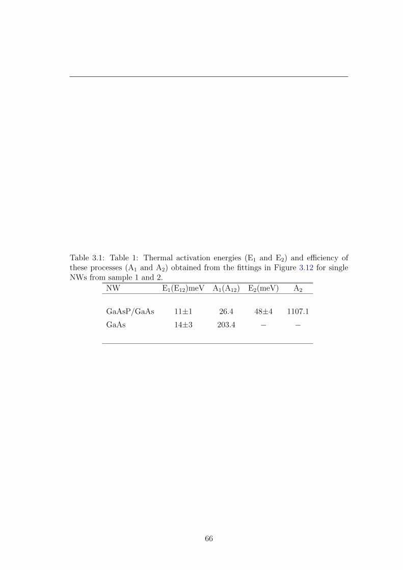
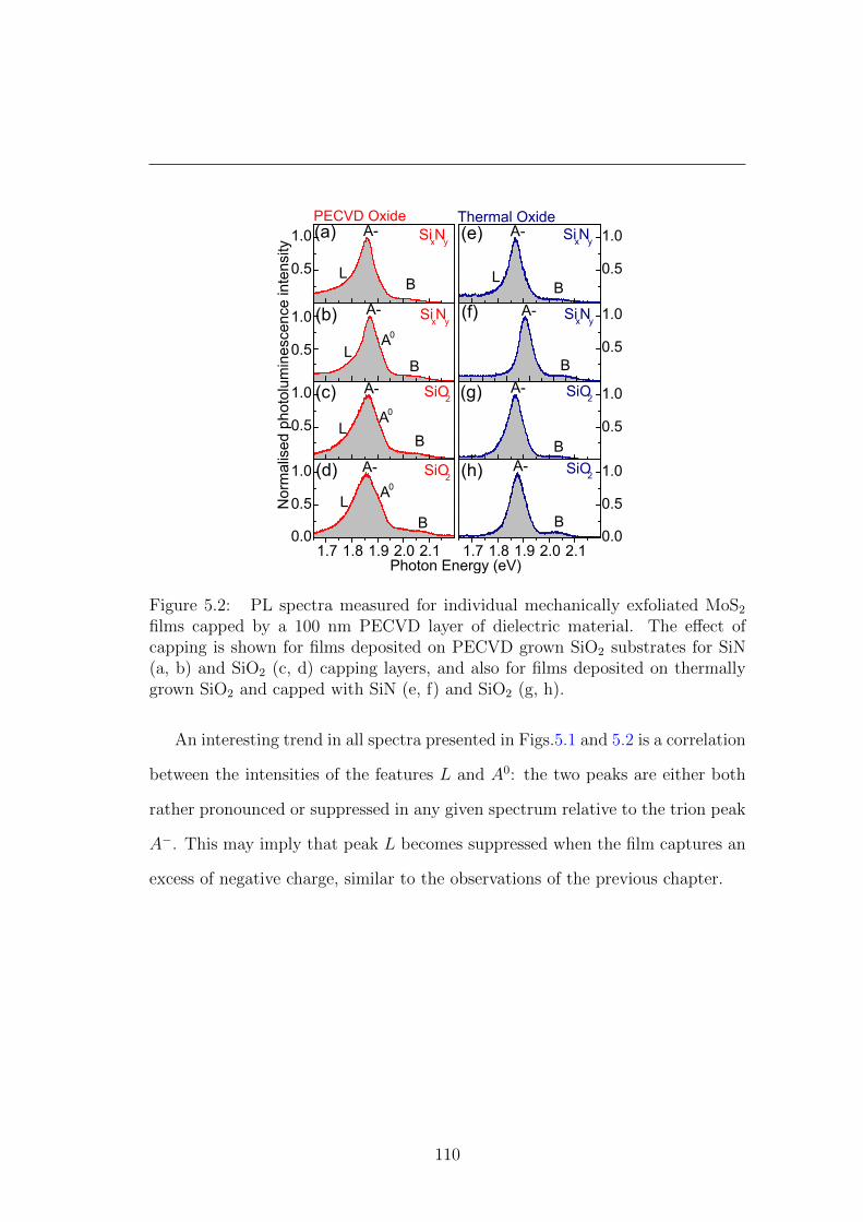
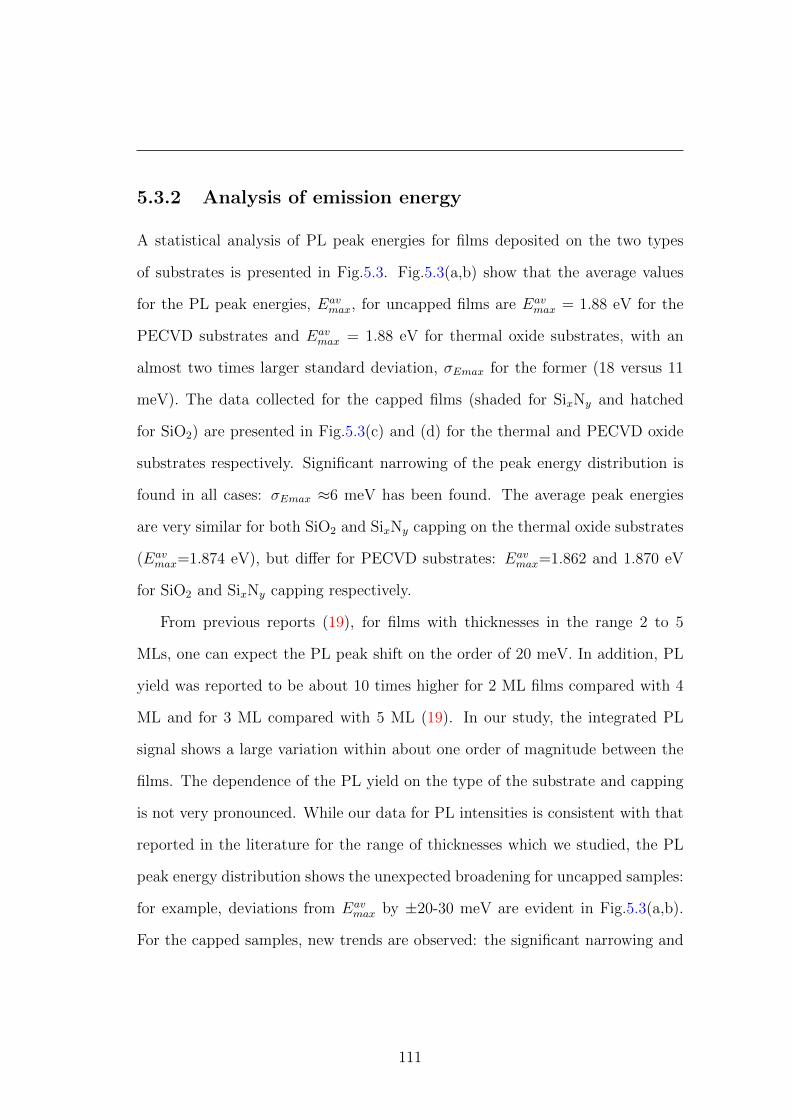
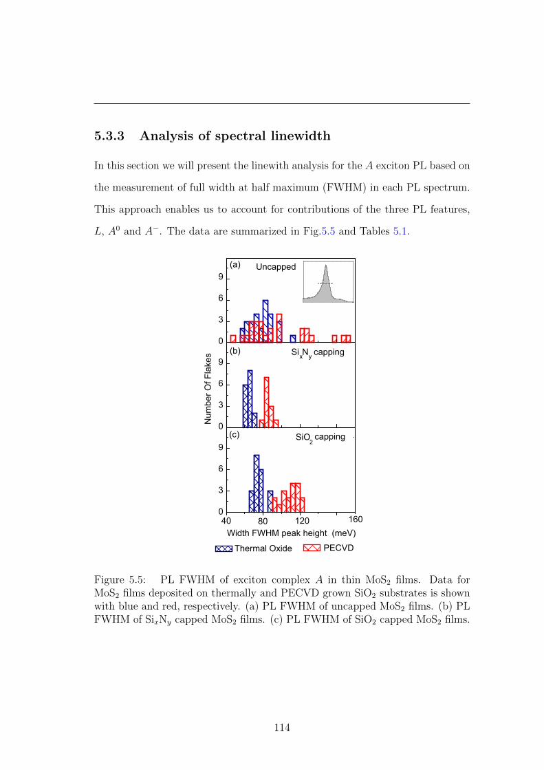
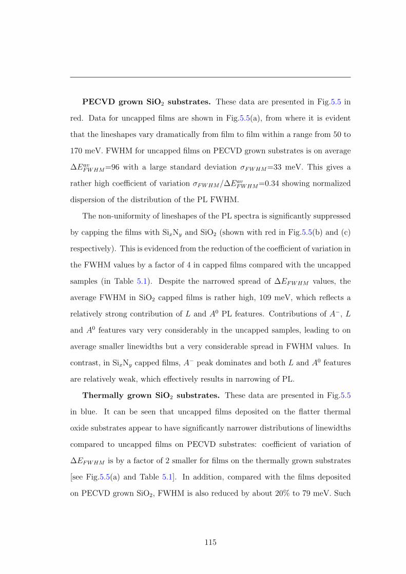
Optical investigations of low-dimensional semiconductor structures Daniel James Sercombe Department of Physics and Astronomy University of Sheffield A thesis submitted for the degree of Doctor of Philosophy September 2013
Transcript
Optical investigations of
low-dimensional semiconductor
structures
Daniel James Sercombe
Department of Physics and Astronomy
University of Sheffield
A thesis submitted for the degree of
Doctor of Philosophy
September 2013
i
I would like to dedicate this thesis to my supportive parents
Sam and Vivienne
and my girlfriend Amy for being so patient.
Acknowledgements
I would like to acknowledge and sincerely thank my supervisor, Alexan-
der Tartakovskii (Sasha), for giving me the opportunity to do this PhD
and for helping me through the last three years. I would also like to
thank Prof. Maurice Skolnick, whose group leadership has allowed me
to learn about and understand other areas of research as well as my
own. I would particularly like to express thanks to Odilon Couto and
Evgeny Chekhovich for their expert teaching, without which I would
not have got so far, as well as their friendship and support. I would
also like to thank EPSRC for providing me with the funding.
I would like to thank my fellow students; S. Schwarz, O. Del Pozo-
Zamudio, F. Liu and J. Puebla, all of whose hard work and dedica-
tion informed the success of this project. I would like to acknowledge
and thank M. Sich and I. Luxmoore for helping to measure data and
for providing experience of time resolved spectroscopy and finally our
collaborators B. J. Robinson and O. Kolosov at the University of Lan-
caster, L. Otubo at the Instituto de Pesquisas Energeticas e Nucleares
IPEN and H.Y. Liu at UCL.
I would like to thank all my friends and colleagues in the LDSD who I
have not already mentioned for making my time in Sheffield so pleas-
ant. In particular I would like to thank A.M. Fox, L.R. Wilson, M.N.
Makhonin, A. Ramsay , P. M. Walker, D.M. Whittaker, Chris, John
Q, John B, Jasmin, Rikki, James, Scott, Ben, Andrew, Lloyd, Deivis,
Maksym, Andreas, Nathan, Tim, Romain, Nikola, Magda and Rob;
the staff of the EPSRC National Centre for III-V Technologies in par-
ticular, Rob Airey, K. Kennedy and John Milner. I would also like to
thank the cryogenics and workshop staff C. Vickers, P. Robinson, P.
Kemp-Russell and Simon Dixon.
Thanks are due also to my friends outside of the LDSD: Tom Dymond,
Emma Parr, Laura Rhodes, Sophy Appleby, Joe Roberts, Rik Bailey,
Ross Carter, Sujit Kumarasinghe, Hannah Gibbs, Liz Double, Toni,
Bob, Tammy, Gaz, Jamie, Dan, Bethan, Rhian, Ana, Katie, Olive,
Matt, my girlfriend Amy and my loving parents!
Daniel Sercombe
Sheffield, 2013.
Abstract
This thesis discusses two optical emitters, gallium arsenide (GaAs)
nano-wires (NWs) and 2D molybdenum disulfide (MoS2) films, which
have the potential to be integrated into silicon (Si) and graphene based
electronics. Optical properties of these systems are studied using a
combination of micro-photoluminescence spectroscopy (µ-PL) and mi-
croscopy techniques to understand the effects of structure and envi-
ronment on light emission. Firstly, it is demonstrated that GaAs NWs
can be grown directly on Si using molecular beam epitaxy (MBE). By
applying a capping material to the NW surface, in this case GaAsP,
we achieve an enhancement of emission yield of up to 104, as well as
a method of controlling emission wavelength through the application
of lattice strain. The second part of this thesis concerns 2D sheets
of MoS2 under 5 atomic layers thick, a direct bandgap semiconduc-
tor which can be integrated into graphene electronics. A method for
producing these films is discussed which utilises breaking of Van der
Waals forces between atomic planes using the mechanical cleavage
technique. In this work we show that the shape of PL emission from
MoS2 is heavily effected by the level of doping in the film, which is
in turn influenced by interactions with dielectric environments. In
the final section of this thesis the problem of irregular emission spec-
tra is addressed and reproducibility of emission properties is found
to increase with the deposition of a dielectric capping layer on the
MoS2 surface. By utilising the subsurface microscopy technique Ul-
trasonic Force Microscopy, we show this improvement occurs due to
increased mechanical bonding between MoS2 and the SiO2 substrate,
which increases the stability of the charge environment.
Publication List
Effect of a GaAsP shell on the optical properties of self-catalyzed GaAs
nanowires grown on silicon
O. D. D. Couto, D. Sercombe, J. Puebla, L. Otubo, I. J. Luxmoore, M. Sich,
T. J. Elliott, E. A. Chekhovich, L. R. Wilson, M. S. Skolnick, H. Y. Liu, A. I.
Tartakovskii
Nano Letters 12 10 52695274 (2012)
Dielectric surface and capping effects on optical properties of a few
atomic monolayer thick MoS2
D. Sercombe, S. Schwarz, Del Pozo-Zamudio, F. Liu, B. J. Robinson, E. A.
Chekhovich, I. I. Tartakovskii, O. Kolosov, and A. I. Tartakovskii
arXiv preprint arXiv:1304.7221 (2013).
Optical Properties Of High Quality GaAs/GaAsP Core-shell Nanowires
on Silicon
D. Sercombe, O. D. D. Couto Jr., J. Puebla, I. J. Luxmoore, M. Sich, L. R.
Wilson, M. S. Skolnick, H. Y. Liu, A. I. Tartakovskii
Presented as a poster at Quantum Dot Day, UCL, London, UK (2012)
Photoluminescence Studies Of Thin Film MoS2
D. Sercombe, O. Del Pozo, E A Chekhovich, F.P Quacquarelli, A. I. Tar-
takovskii, M.S. Skolnick
Presented as a poster at UK Semiconductors (conference), Sheffield, UK (2012)
v
Dielectric substrate and capping effects on optical properties of a few
atomic monolayer MoS2 sheets (I)
D. Sercombe, S. Schwarz, Del Pozo-Zamudio, F. Liu, B. J. Robinson, E. A.
Chekhovich, I. I. Tartakovskii, O. Kolosov, and A. I. Tartakovskii
Presented as a poster at Graphene Week, Chemnitz, Germany (2013)
Dielectric substrate and capping effects on optical properties of a few
atomic monolayer MoS2 sheets (II)
D. Sercombe, S. Schwarz, Del Pozo-Zamudio, F. Liu, B. J. Robinson, E. A.
Chekhovich, I. I. Tartakovskii, O. Kolosov, and A. I. Tartakovskii
Presented as a poster at EP2DS-MSS, Wroclaw, Poland (2013)
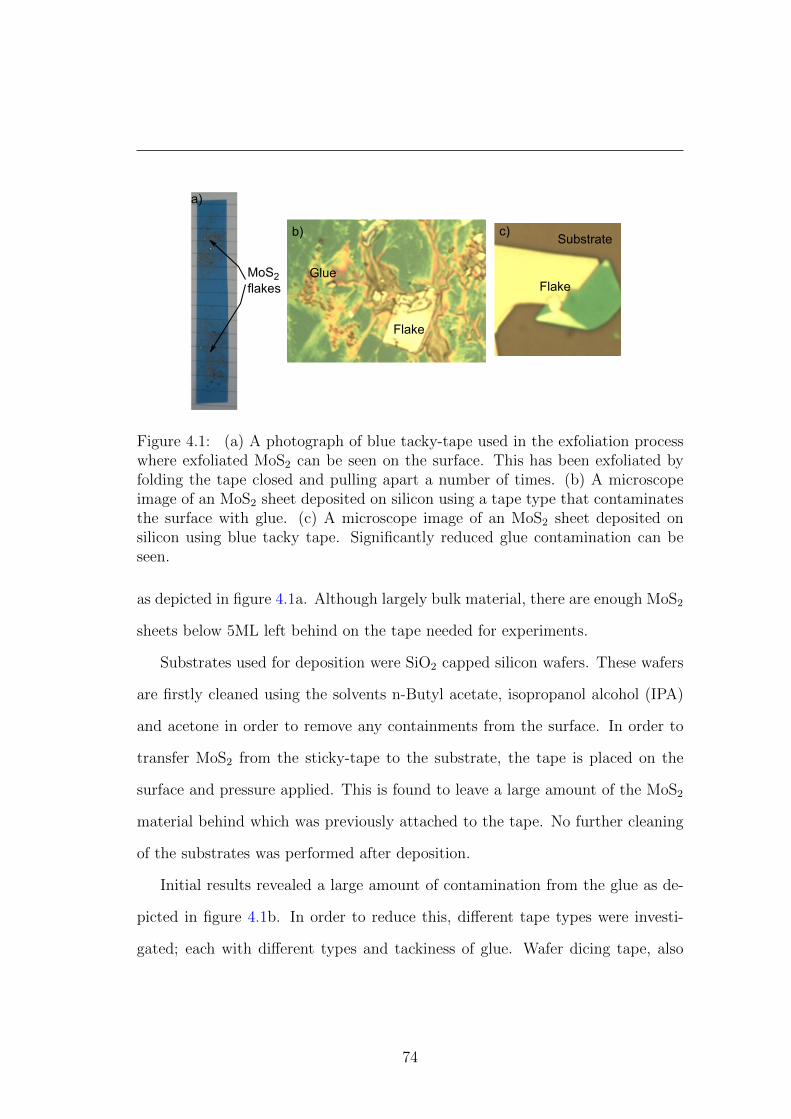
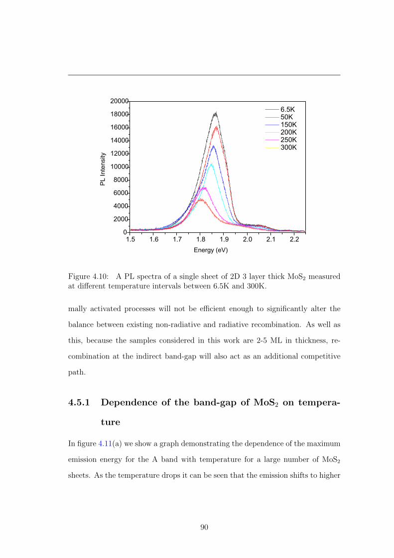
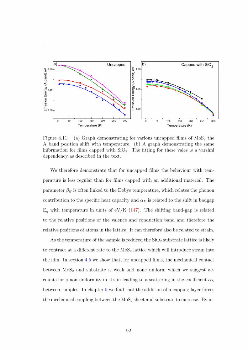
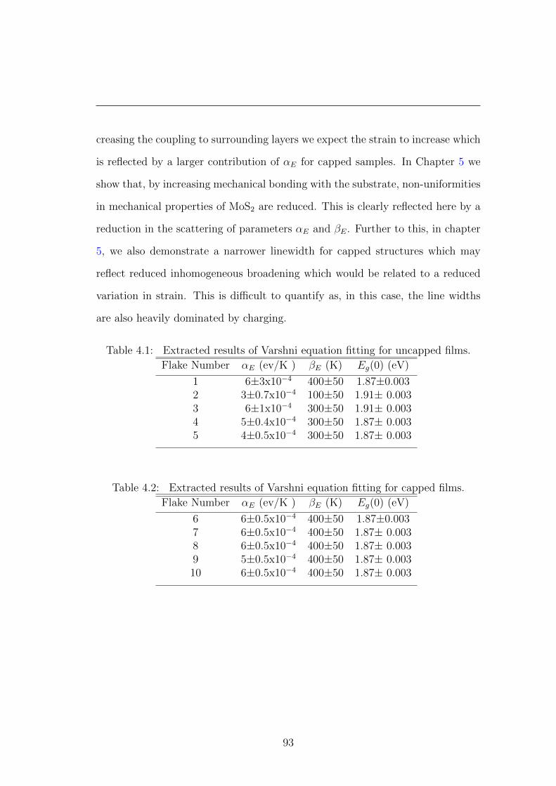
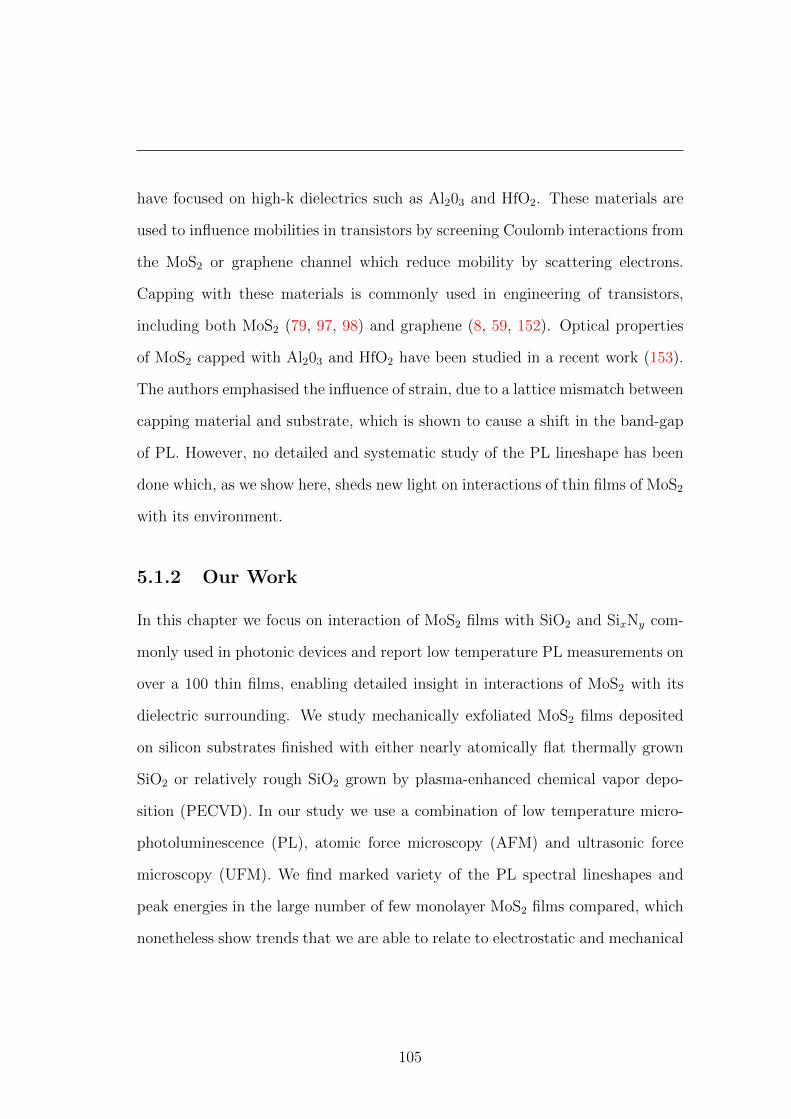
Modern electronics rely on logic circuits based on silicon field effect transistors
developed for the first time in the 1950s (1, 2). Current technological goals fo-
cus on improving speed, cost, power consumption and miniaturization of circuit
applications and the direct integration of photonics (3). This is a wide area of
research which covers advances in fields such as spintronics (4), photonics (5),
quantum computing (6, 7) and graphene based electronics (8). Another large
area of semiconductor research concerns photovoltaics (9, 10). The generation
of electrical power by conversion of solar radiation may be an important step
in developing greener alternatives to fossil fuels (11). Research into these ar-
eas require a strong understanding of the properties of semiconductor materials,
structures and devices (12). Novel nano-structures are at the forefront of research
and these include quantum dots (13, 14), quantum nanowires (9, 15), quantum
wells (16, 17) and atomic monolayers (8, 18).
This thesis focuses on the effects of crystalline structure and environment on
1
electronic and optical properties of semiconductor nano-structures. This is stud-
ied using a combination of optical spectoscopy and various microscopy techniques.
The microscopy techniques used are transmission electron microscopy (TEM),
scanning electron microscopy (SEM), atomic force microscopy (AFM) and ultra-
sonic force microscopy (UFM). Optical properties are studied using continuous
wave (CW) and time resolved (TR) micro-photoluminescence spectroscopy (PL).
The first part of this thesis covers GaAs nano-wires grown directly on silicon
wafers and the second half covers optical properties of thin films of MoS2, a ma-
terial which recently was shown to have a transition to direct band-gap for few
atomic monolayer thicknesses (19, 20).
2
1.2 III-V nanowires grown on silicon substrates
Nanowires (NWs) are a one dimensional nano-structure with a high length to
diameter aspect ratio. Due to low dimensions NWs exhibit unique optical and
electronic properties different from the bulk material. In this chapter we review
interest in III-V semiconductor NWs which have potential uses in optoelectronics
(21, 22) and photovoltaics (9, 23, 24). We focus on the integration of III-V NWs
onto silicon substrates as this has the potential to significantly reduce the cost of
devices. In particular we highlight the advantages of growing these NWs using a
recently developed catalyst free molecular beam epitaxy (MBE) method. We then
discuss the effects that crystalline structure, determined during growth, and the
addition of a nanowire shell has on photoluminescence. In Chapter 3 we continue
work on nanowires by investigating, for the first time, the optical properties of
GaAs/GaAsP core-shell nanowires grown by this method on Si substrates.
1.2.1 Interest in III-V Nanowires grown on silicon
III-V materials, such as GaAs, GaN, InAs and InP, are direct bandgap semicon-
ductors and therefore have bright photoluminescence (PL) and electrolumines-
cence (12, 25, 26, 27). This property, discussed in more detail in section 2, has
therefore allowed III-V materials to form the basis of many optoelectronic devices
(21, 28, 29). Although so far no commercial devices based on III-V nanowires
(NWs) are available (21), optical devices such as light emitting diodes (LEDs)
(30, 31), electrically driven lasers (32) and photon detectors (33) have already
been developed for research purposes. Growing nanowire heterostructures with
embedded quantum dots may also be an important step for controlling the posi-
3
tion and dimensions of III-V quantum dots in photonic structures (34, 35, 36).
Current electronics are based on silicon technology because this is cost effective
to produce (37). Si is an indirect band-gap material and therefore has only very
weak optical emission (25). Integrating more expensive III-V photonics directly
into silicon devices is therefore advantageous but it is difficult to achieve due to
lattice mismatch, which is particularly large in the case of GaAs studied here (38).
This leads to the formation of dislocations (39) between epitaxial layers during
deposition and overcoming this require complicated growth patterns with limited
success (40) or wafer bonding which is a costly process (41). III-V semiconductor
NWs are naturally less reliant on lattice matching with the growth substrate as
the narrow NW diameter allows radial variations which relieve strain without
forming dislocations (22). Growing NWs directly on Si may therefore provide
a future cost effective method for direct integration of III-V photonics into Si
electronics (22).
NWs have been earmarked for future use in efficient photovoltaics. The global
demand for energy is increasing rapidly and predicted to hit 30TW by 2050,
double the current value (42), and solar energy is one of the most promising
renewable energy sources. The main disadvantage of current solar devices is that
they have unsustainably high production costs (43) compared to an extremely
low efficiency of light-to-electricity conversion (44). The limit on efficiency for
current p-i-n devices is only ∼30%. There are therefore two criteria for creating
new sustainable devices, increasing efficiency and reducing costs. The efficiency of
current devices is limited by the ray optics limit, which is the minimum thickness
needed to fully absorb the solar spectrum (45). The high length-to-diameter
ratio of NWs allows a tailored thickness to enhance optical absorption (44) and
4
therefore exceed this ray optics limit (46). This is particular promising when
considering dense NW arrays (43). The small dimension of NWs also allows for
small electron collection lengths which also heavily effects the efficiency of current
devices (9, 46).
Recent developments in growing III-V NWs directly onto silicon and also
exceptional new results showing up to 71% efficiency for absorbed light converted
to electrical current in a single NW (46) may therefore point towards a future for
producing highly efficient and cost effective photovoltaics (10, 23).
1.2.2 Fabrication of III-V nanowires, with a focus on
growth on silicon.
Good quality NWs for use in photonics and photovoltaics require well controlled
dimensions. For example, variations in axial width can lead to effects such as inho-
mogeneous broadening of photoluminescence (PL) emission (described in section
2.1). Stacking defects can act as charge traps (47) which will effect radiative
recombination and photovoltaic efficiency. The structure of NWs is further com-
plicated as two different crystal lattices, zinc-blend (ZB) and wurtzite (WZ),
can form (47, 48). These have a different band-gap and therefore greatly effect
electronic and optical properties of the NW, as discussed in section 1.2.3.
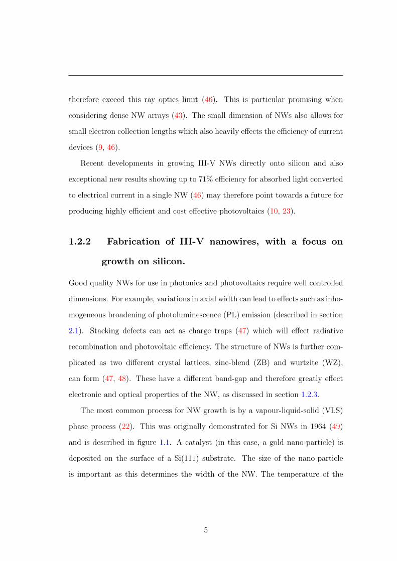
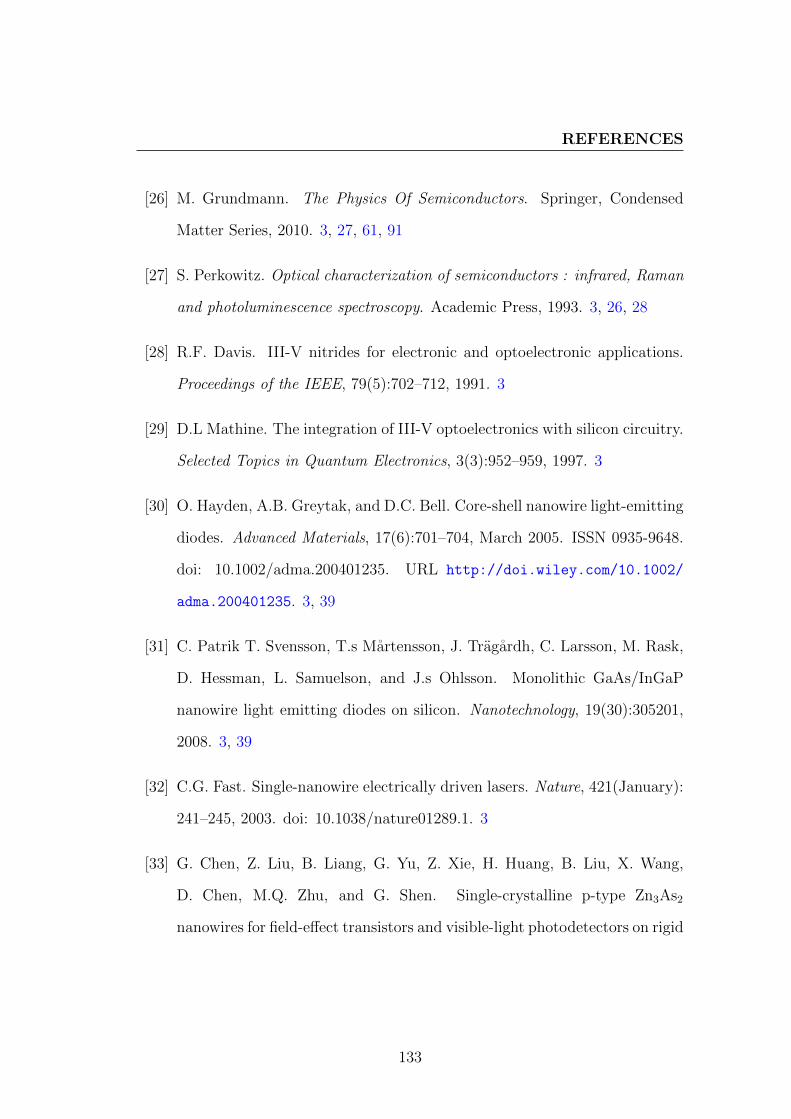
The most common process for NW growth is by a vapour-liquid-solid (VLS)
phase process (22). This was originally demonstrated for Si NWs in 1964 (49)
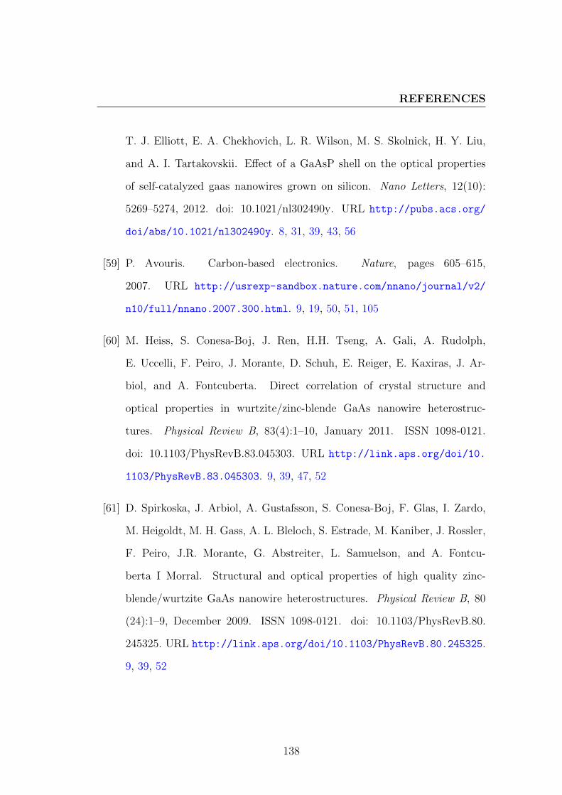
and is described in figure 1.1. A catalyst (in this case, a gold nano-particle) is
deposited on the surface of a Si(111) substrate. The size of the nano-particle
is important as this determines the width of the NW. The temperature of the
5
Silicon Substrate
Gold nanoparticle Au-Si alloy (liquid)
Si (Vapour)
Au-Si alloy (liquid)
Siliconcrystal(solid)
a) b) c)
Figure 1.1: A diagram demonstrating the growth of silicon NWs using the vapour-liquid-solid (VLS) method. (a) Firstly, gold particles are deposited on the sub-strate to act as catalysts for growth. (b) High temperatures melt the Au particles,creating a liquid phase. The growth constituent Si, in a vapour form, is directedat the substrate by either MBE or MOVPE. (c) Si vapour is absorbed by the liq-uid Au forming a solution. When this solution becomes super-saturated a solidlayer is deposited beneath the Au eventually forming a NW.
substrate is then raised and the gold nano-particle melts. To begin growth, Si is
released into the growth chamber in a vapour-phase. This is commonly achieved
by either molecular beam epitaxy (MBE) (50) or metalorganic chemical vapour
deposition (MOVPE) (38). The Si vapour is then absorbed by the liquid gold
forming a solution. As more vapour is added, the solution becomes supersaturated
and Si is deposited in the interface between the gold and the substrate. By
continuing to feed supersaturation a solid NW will grow beneath the liquid-phase
of the catalyst. Radial growth of NWs (which causes effects such as tapering)
can be kinetically controlled by using high temperatures and also by controlling
the rate of deposition (38).
This method can be adapted to grow III-V material NWs directly onto Si, such
6
as GaP (38), InAs (51) and GaAs (50). By changing the constituent elements,
heterostructure NWs with embedded quantum dots can be achieved (35, 36).
Gold nano-particle assisted growth is currently the most common method used
in research (22). A high accuracy, low defect density and narrow diameter down
to 20nm (38) has been achieved. However, the gold catalyst can contaminate the
purity of the crystal structure (42) which will likely affect electrical properties and
may have adverse effects on photovoltaics. There is therefore a current drive to
develop catalyst-free growth methods which have comparable quality and growth
control.
The first catalyst free method demonstrated for III-V NWs on Si uses the
deposition of a thin organic film to create growth sites on the substrate (52). The
Si substrate is firstly HF etched to remove all oxides from the surface. Organic
material is then deposited by spin coating and forms a natural mask where small
nm regions are covered. The Si surface is then allowed to oxidise again, except
in the regions covered by organic material. The sample is placed in a vacuum
to remove remaining organic material by in-situ annealing. When III-V elements
are released by MOVPE, they diffuse across the SiO2 surface and form clusters in
the less oxide regions where the polymer was, which act as growth sites for NWs.
III-V materials grown on Si by this method include InAs (52, 53) and GaAs (54).
Unfortunately NWs grown by this method are found to have relatively larger
diameters (50nm+) and uncontrollable stacking defects (53).
A more recently demonstrated self-seeded MBE growth method (55) may
therefore be the next step in developing catalyst free III-V semiconductors on
silicon. This growth utilises the VLS method described above, but instead of a
Au nanoparticle a droplet of a constituent element is used. So far this has only
7
been demonstrated for GaAs NWs (55, 56, 57, 58) and the constituent used in
this case is always Ga. NWs produced by this method have demonstrated good
control over crystal structure, low defects and narrow diameters (20nm) similar
to gold catalysed methods (56). This is the method we consider in our work, and
more details of our growth procedure are presented in Chapter 3.
1.2.3 Structural effects on optical properties of III-V
nanowires
In this section we consider structural effects on the PL properties of NWs, look-
ing specifically at results for III-V NWs grown on Si which are available in the
literature. We firstly consider the effect of crystal phase polytypes WZ and ZB
and then, by considering core-shell structures, we explore the effect of surface
states on NWs. These observations are directly relevant to observations made in
our work on catalyst free GaAs and GaAs/GaAsP NWs presented in Chapter 3.
1.2.3.1 Effect of crystal phase polytypes on optical properties of III-V
nanowires
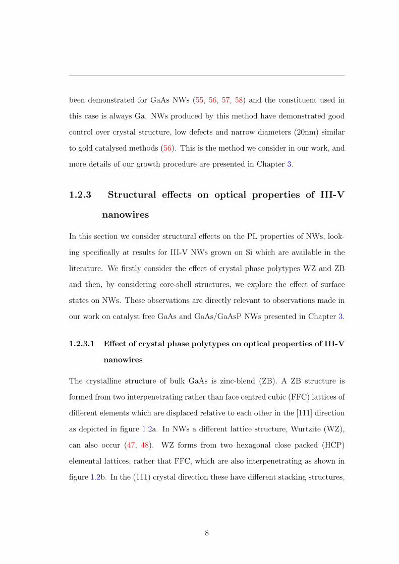
The crystalline structure of bulk GaAs is zinc-blend (ZB). A ZB structure is
formed from two interpenetrating rather than face centred cubic (FFC) lattices of
different elements which are displaced relative to each other in the [111] direction
as depicted in figure 1.2a. In NWs a different lattice structure, Wurtzite (WZ),
can also occur (47, 48). WZ forms from two hexagonal close packed (HCP)
elemental lattices, rather that FFC, which are also interpenetrating as shown in
figure 1.2b. In the (111) crystal direction these have different stacking structures,
8
a) b)
Figure 1.2: Diagrams showing the crystal structure of (a) zinc-blende and (b)wurtzite phases. The crystal lattice of zinc-blende is face centre cubic and thecrystal lattice of wurtzite is hexagonal close packed.
which are ABCABC stacked for ZB and ABABAB for WZ (59) where A, B and
C are repeating stacking structures. The phase of the entire NW crystal, or
the density of ZB/WZ planes, can be controlled during both Au and catalyst
free VLS growth techniques by varying the vapour-phase deposition speed and
temperature (22, 56).
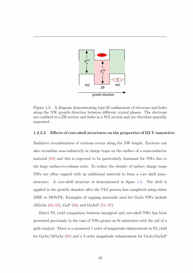
There is a 115meV offset between the band edges of ZB and WZ and quantum
confinement can occur, along the NW length, between different sections if both
are present (47, 60). In this case holes are confined in the valence band of WZ
segments and electrons in the conduction of ZB segments (61) as shown in figure
1.3. Electrons and holes are therefore spatially separated and this is known as
type-II confinement. For NWs where the radius of the NW is smaller than the
radius of excitons, quantum confinement can also occur radially. In structures
where both types of confinement occur strongly, the electron will be effectively
confined in three dimensions in a system which has been dubbed as a crystal
phase quantum dot. This has been observed for VLS Au assisted grown InP
NWs (62).
9
EgWZ
EgZB
e
h
WZZB
WZ
growth direction
Figure 1.3: A diagram demonstrating type-II confinement of electrons and holesalong the NW growth direction between different crystal phases. The electronsare confined in a ZB section and holes in a WZ section and are therefore spatiallyseparated.
1.2.3.2 Effects of core-shell structures on the properties of III-V nanowires
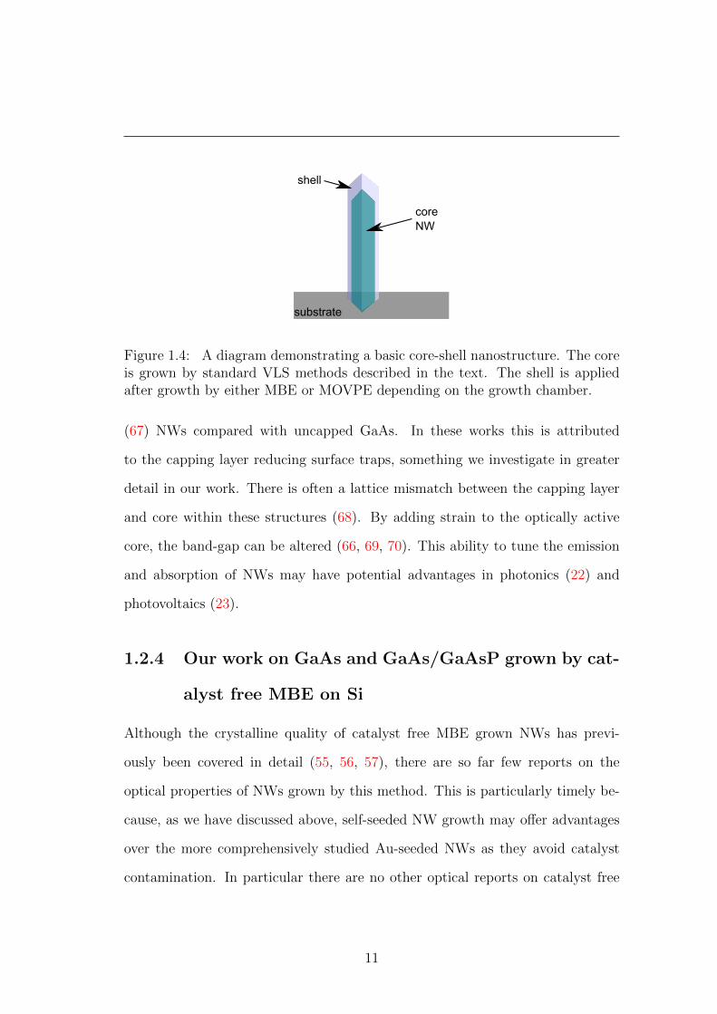
Radiative recombination of excitons occurs along the NW length. Excitons can
also recombine non-radiatively in charge traps on the surface of a semiconductor
material (63) and this is expected to be particularly dominant for NWs due to
the large surface-to-volume ratio. To reduce the density of surface charge traps
NWs are often capped with an additional material to form a core shell nano-
structure. A core-shell structure is demonstrated in figure 1.4. The shell is
applied in the growth chamber after the VLS process has completed using either
MBE or MOVPE. Examples of capping materials used for GaAs NWs include
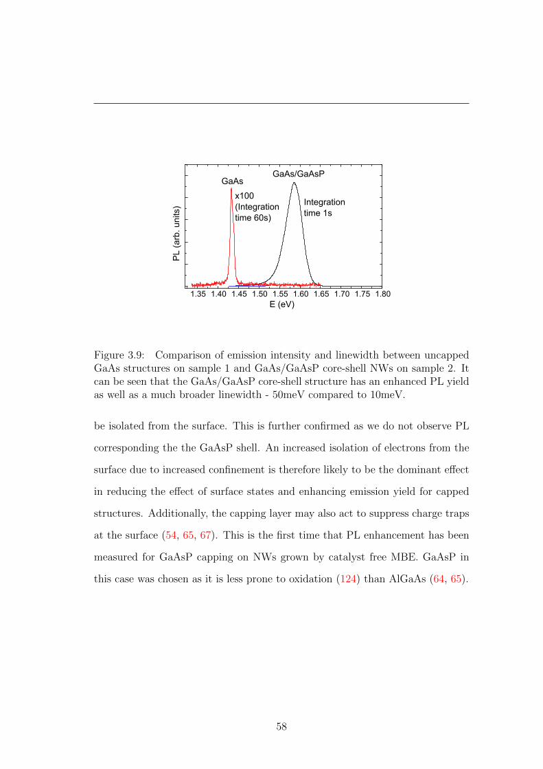
AlGaAs (64, 65), GaP (66) and GaAsP (54, 67).
Direct PL yield comparison between uncapped and core-shell NWs has been
presented previously in the case of NWs grown on Si substrates with the aid of a
gold catalyst. There is a measured 1 order of magnitude enhancement in PL yield
for GaAs/AlGaAs (65) and a 2 order magnitude enhancement for GaAs/GaAsP
10
substrate
shell
coreNW
Figure 1.4: A diagram demonstrating a basic core-shell nanostructure. The coreis grown by standard VLS methods described in the text. The shell is appliedafter growth by either MBE or MOVPE depending on the growth chamber.
(67) NWs compared with uncapped GaAs. In these works this is attributed
to the capping layer reducing surface traps, something we investigate in greater
detail in our work. There is often a lattice mismatch between the capping layer
and core within these structures (68). By adding strain to the optically active
core, the band-gap can be altered (66, 69, 70). This ability to tune the emission
and absorption of NWs may have potential advantages in photonics (22) and
photovoltaics (23).
1.2.4 Our work on GaAs and GaAs/GaAsP grown by cat-
alyst free MBE on Si
Although the crystalline quality of catalyst free MBE grown NWs has previ-
ously been covered in detail (55, 56, 57), there are so far few reports on the
optical properties of NWs grown by this method. This is particularly timely be-
cause, as we have discussed above, self-seeded NW growth may offer advantages
over the more comprehensively studied Au-seeded NWs as they avoid catalyst
contamination. In particular there are no other optical reports on catalyst free
11
GaAs/GaAsP core-shell structures produced in an MBE system. In Chapter 3
we present new in-situ micro-PL measurements on individual free standing GaAs
and GaAs/GaAsP NWs grown by this method and demonstrate the effects of
surface and structure on optical properties.
We find that while our uncapped GaAs NWs have a relatively small PL yield,
our core-shell GaAs/GaAsP NWs have, in comparison, a PL yield enhancement
exceeding 2000x. We observe that the addition of the GaAsP capping layer in our
core shell structures leads to a reduction in the efficiency of thermal activation for
non-radiative processes by a factor of 8, suggesting that these states are on the
NW surface. We also find that additional charge traps can form on the surface
of an uncapped NW which is exposed to air, a process we attribute to oxidation.
Both of these observations therefore provide evidence that a weak PL yield in
uncapped GaAs NWs is due to the effects of non-radiative surface states.
PL signal up to room temperature. By considering the activation of PL quenching
mechanisms with temperature, we demonstrate a new quenching process at high
temperature which we attribute to electrons escaping from the GaAs core into
the GaAsP shell. We also find that the addition of GaAsP shell imparts strain
on the NW core, which is evident due to a blue shift of PL above the band gap of
zinc blende GaAs. Varying the nominal concentration of P in the capping shell
may prove to be a useful method for strain-tuning the NW band-gap.
Additionally, to surface effects and strain, we demonstrate the effect of type-
II confinement, between WZ and ZB, for NWs grown by our method. This
is concluded from relatively long lifetimes measured and also a shift in emission
energy below the value for GaAs ZB, which reflects a previously accepted 115meV
12
band offset between GaAs WZ and ZB. The PL lifetime measured is 7.4ns for
type-II confinement. For NWs grown at a slightly higher temperature (640oC
compared to 635oC) we find pure ZB phase structures with lifetimes measured at
1.43ns.
13
1.3 MoS2, a new direct band-gap semiconductor
Since its discovery, graphene has been suggested as the next step in developing
high speed electronics due to its large conductivity (8, 71). There is a large
family of other 2D materials that can be prepared similarly to graphene in a
quasi-2D form including MoS2 (19), MoTe2 (72), WS2 (73), boron nitride (74)
and many more. Future devices may rely on combining electronic properties
of these materials with the large conductivities found in graphene in stacked
heterostructures (75, 76, 77, 78). It is therefore important to understand the
properties of these materials and in Chapter 4 and 5 we look in detail specifically
at molybdenum disulfide (MoS2).
Particular interest in two-dimensional thin films of MoS2 has formed due to the
discovery of an indirect to direct band-gap transition for thicknesses less than 10
atomic layers, leading to observed bright photo-luminescence (PL) (19, 20) as well
as attractive field effect transistor (FET) behaviour (79, 80, 81, 82, 83). A high
Earth abundance of the material (80), relative inexpense and ease of production of
2D structures (84) make MoS2 a desirable material for both research and potential
industrial applications. The demonstration of optical valley polarization (85, 86,
87, 88) and high flexibility and strain tuning (89) suggest future applications in
valleytronic devices and flexible electronics respectively; and bright PL emission
may be used in optoelectronics (90).
In this section we discuss the recent interest in the optical and electronic
properties of MoS2 by reviewing the work available in literature. Our work on
MoS2 is continued in Chapter 4 and 5 where we explore in detail the processes
14
that influence the shape of PL spectra with a particular emphasis on interactions
with Si/SiO2 substrates. Functionality of MoS2 as a lubricant (91), catalyst (92)
and in nanotube form (93) have also been demonstrated but are beyond the scope
of this work.
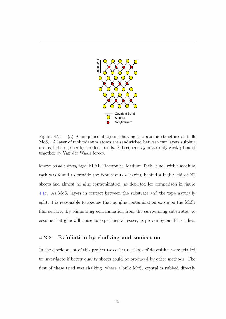
1.3.1 Structural properties of MoS2
Sulphur
Molybdenum
sing
le la
yer
Covalent Bond
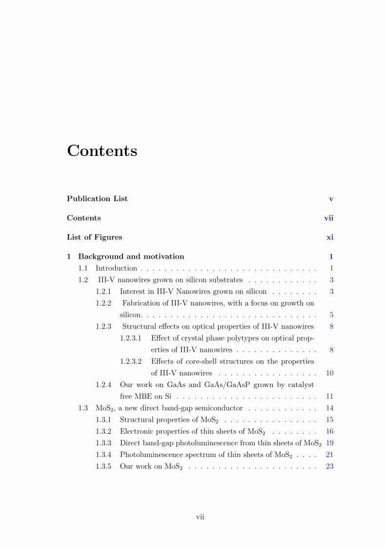
Figure 1.5: (a) A simplified diagram of the structure of MoS2. Molybdenumatoms are sandwiched between a layer of Sulphur atoms which they are covalentlybonded to. This forms a single layer as labelled. Each subsequent layer is thenstacked and bonded by weak Van der Waal interactions.
MoS2 is a dichalcogenide compound made from transition metal molybdenum
(Mo) and chalcogen non-metal sulphur (S). A diagram of the lattice structure of
MoS2 is provided in figure 1.5. It can be seen here that Mo atom is covalently
bonded to S forming a single layer where Mo sits in the centre and S at the
edges (94). Each subsequent layer is only weakly bonded to surrounding layers
by electrostatic dipole forces known as Van der Waals. Due to the weak bonds
15
between the layers, it is possible to reduce them down to 2D sheets featuring few
to a single individual layer known as a monolayer (ML). Exfoliation of MoS2 will
be described in detail in Chapter 4, where we demonstrate the method developed
for this project.
The MoS2 used in this work was from a mineral source of unknown purity.
Defects may act as sources of n or p charges within the samples. These impurities
can therefore effect the electronic and PL properties. This is particularly impor-
tant in our work, as we will discuss below, because we find that the spectrum of
MoS2 is dominated by a charged exciton peak.
1.3.2 Electronic properties of thin sheets of MoS2
Transistors are very important in modern electronics for use in both logic circuits
and as radio-frequency amplifiers (37). Metal-Oxide Semiconducting Field Effect
Transistors (MOSFET) are currently the most widely used design (12). These
feature a source (s) and drain (d) contact connected by a channel (c) where the
current flows. The flow of electrons in the channel is controlled by a gate voltage
(g) (95). A MOSFET has two modes of operation, on and off. Logic gates used in
modern computing are constructed from a series of MOSFETs, which are usually
produced on chip. These form the backbone of modern computing.
For good quality logic circuits FET devices require good conductivity (product
of charge density and mobility) and high switching described by a good ON/OFF
ratio between currents ION and IOFF (80). A low current is especially desirable
for the off state of FETs due to the power saving advantages. Semiconductor
materials are highly desirable for use in FET transistors as they have good trans-
16
port for electrons and low off current due to the fact that electrons need to be
promoted across a bandgap before a current can flow (96). The most commonly
used semiconductor in modern MOSFET devices is Silicon (12).
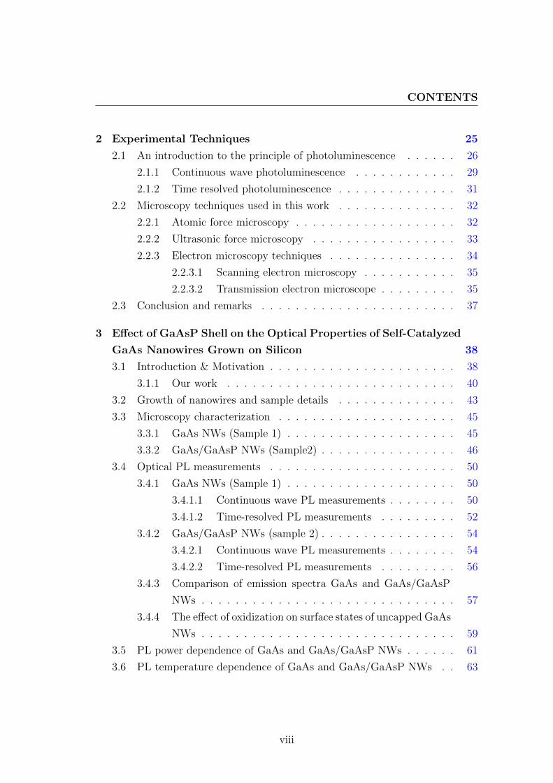
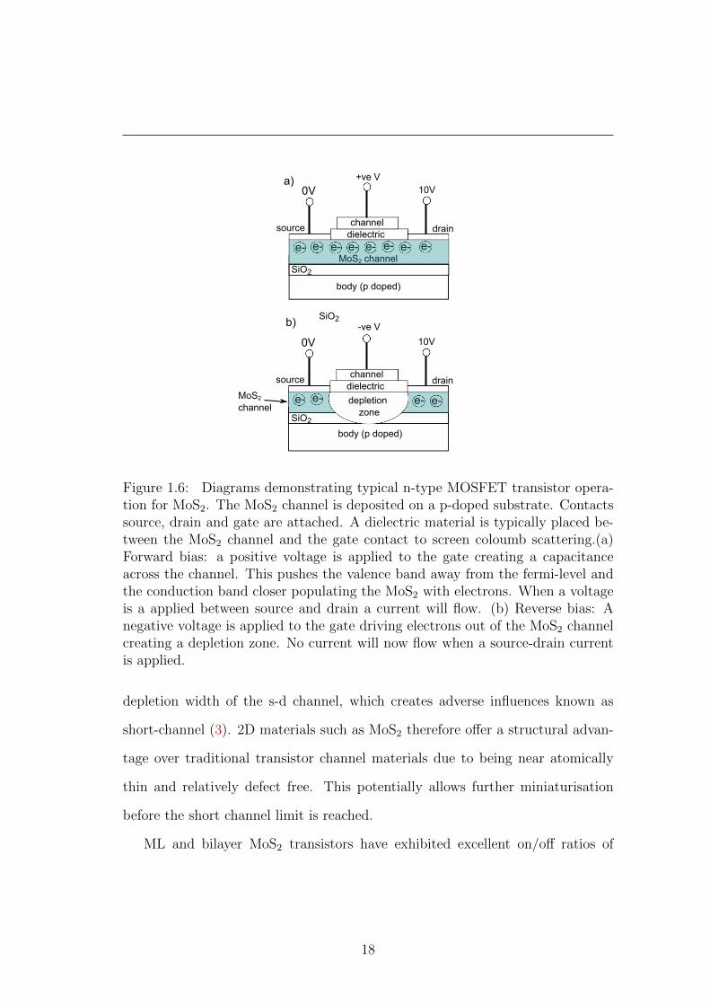
A diagram of a typical n-type MoS2 FET is given in figure 1.6. Here a ML of
MoS2 has been deposited on a p-doped silicon wafer. Au contacts are deposited
by electron beam lithography (79). A high-k dielectric such as HfO2 is deposited
between the MoS2 channel and gate contact to screen coulomb interactions which
effect the carrier mobility (81). The width of the MoS2 channel, where current
is allowed to flow, is controlled by creating a capacitance between the gate and
substrate, which causes bending of the valence and conduction levels (82). In-
troducing a sufficiently large positive gate voltage (with respect to the source)
pushes the valence band away from the fermi level (driving holes away from the
gate) and the conduction band closer populating the MoS2 with electrons (95).
This creates a conducting channel and a current can therefore flow when a voltage
is applied between the source and drain (figure 1.6a). Applying a negative volt-
age has the opposite effect, effectively driving electrons from the semiconductor
channel creating a depletion zone (figure 1.6b). In the ideal case no current will
flow in this mode regardless of voltage between the source and drain.
With modern technology requiring increasing computing capabilities within
smaller devices there is a current industrial drive for miniaturisation of FETs
which MoS2 may fulfil. In III-V materials and silicon reducing the height of the
channel reaches a limit where rough interfaces and thickness variations related
to growth become an issue; leading to reduced mobility and large threshold volt-
age variations (8). When reducing the length of a FET channel we therefore
reach a limit where the channel length has the same order of magnitude of the
17
0V 10V
source drainchannel
dielectrice-e- e- e- e- e- e- e-
+ve V
MoS2 channel
body (p doped)
0V 10V
source drain
e-e- e- e- e- e- e-
-ve V
channel
body (p doped)
e-
channeldielectric
a)
b)
MoS2 channel
SiO2
SiO2
SiO2
depletion zone
Figure 1.6: Diagrams demonstrating typical n-type MOSFET transistor opera-tion for MoS2. The MoS2 channel is deposited on a p-doped substrate. Contactssource, drain and gate are attached. A dielectric material is typically placed be-tween the MoS2 channel and the gate contact to screen coloumb scattering.(a)Forward bias: a positive voltage is applied to the gate creating a capacitanceacross the channel. This pushes the valence band away from the fermi-level andthe conduction band closer populating the MoS2 with electrons. When a voltageis a applied between source and drain a current will flow. (b) Reverse bias: Anegative voltage is applied to the gate driving electrons out of the MoS2 channelcreating a depletion zone. No current will now flow when a source-drain currentis applied.
depletion width of the s-d channel, which creates adverse influences known as
short-channel (3). 2D materials such as MoS2 therefore offer a structural advan-
tage over traditional transistor channel materials due to being near atomically
thin and relatively defect free. This potentially allows further miniaturisation
before the short channel limit is reached.
ML and bilayer MoS2 transistors have exhibited excellent on/off ratios of
18
108 (79), with ratios above 104 (59, 90) being generally accepted as good for
transistor switches. Mobilities in MoS2 of 200 cm2V−1s−1 (79, 97, 98) have been
demonstrated with a limit calculated at 410 cm2V−1s−1 (82). Direct comparisons
with silicon transistors in the same dimensions have been performed by Alam
et al. (82). Here they find a steeper sub-threshold slope (which characterises
faster switching between on/off states), reduction in S-D leakage and shorter
possible channel lengths in the case of MoS2. This is, in part, related to the
heavier effective mass and this work suggests that MoS2 is a viable candidate for
replacing silicon due to it’s improved functionality in small dimensions (99).
1.3.3 Direct band-gap photoluminescence from thin sheets
of MoS2
A bright PL signal is found for thin films of MoS2. This arises from a change in
the material band-structure when compared to thicker sheets (above 10 layers)
and bulk. Calculations of the band structure for MoS2 (20, 100, 101, 102) have
demonstrated a shift from an indirect optical bandgap (described in section 2.1)
in bulk material to a direct bandgap for a single layer (100).
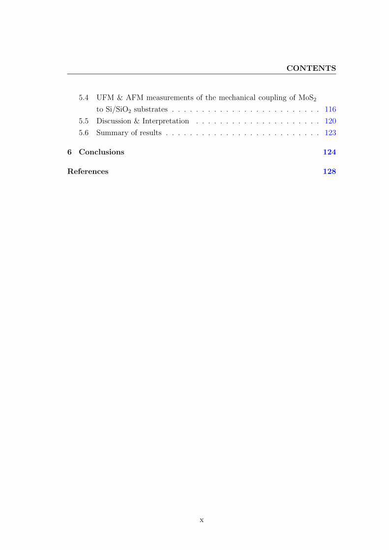
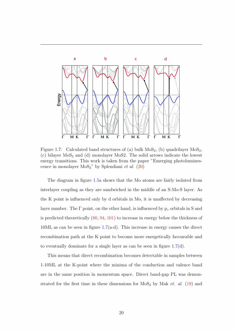
An example of calculated band structures for (a) bulk, (b) quadrilayer, (c)
bilayer and (d) monolayer MoS2 from the work of Splendiani et al. (20) is shown
in figure 1.7. In MoS2 the indirect band-gap in bulk material occurs at the Γ
point of the valence band in k-space as can be seen in (a). States at the Γ point
are a combination of antibonding pz orbitals in the S atoms and d orbitals in Mo.
In contrast states at the K point (where direct recombination occurs in MoS2)
occur only due to the d orbitals in Mo atoms (80).
19
Figure 1.7: Calculated band structures of (a) bulk MoS2, (b) quadrilayer MoS2,(c) bilayer MoS2 and (d) monolayer MoS2. The solid arrows indicate the lowestenergy transitions. This work is taken from the paper ”Emerging photolumines-cence in monolayer MoS2” by Splendiani et al. (20)
The diagram in figure 1.5a shows that the Mo atoms are fairly isolated from
interlayer coupling as they are sandwiched in the middle of an S-Mo-S layer. As
the K point is influenced only by d orbitals in Mo, it is unaffected by decreasing
layer number. The Γ point, on the other hand, is influenced by pz orbitals in S and
is predicted theoretically (80, 94, 101) to increase in energy below the thickness of
10ML as can be seen in figure 1.7(a-d). This increase in energy causes the direct
recombination path at the K point to become more energetically favourable and
to eventually dominate for a single layer as can be seen in figure 1.7(d).
This means that direct recombination becomes detectable in samples between
1-10ML at the K-point where the minima of the conduction and valence band
are in the same position in momentum space. Direct band-gap PL was demon-
strated for the first time in these dimensions for MoS2 by Mak et. al. (19) and
20
Splendiani et. al (20) in 2010. They found that with increasing thickness from a
single layer the energy gap of the indirect path decreases on a layer-by-layer basis
meaning that direct emission becomes less energetically favourable. This results
in PL yield from direct recombination decreasing with increasing thickness from a
single monolayer, which they measure to be nearly exponential. Subsequent time
resolved measurements of emission from the direct band-gap of MoS2 have shown
recombination times of 5ps between 4.5-150K and 70 ps for room temperature
(103).
1.3.4 Photoluminescence spectrum of thin sheets of MoS2
Due to the relative infancy of this field, there are still very few reports focussing
on PL from MoS2 (19, 20, 85, 103, 104) which are always measured for samples
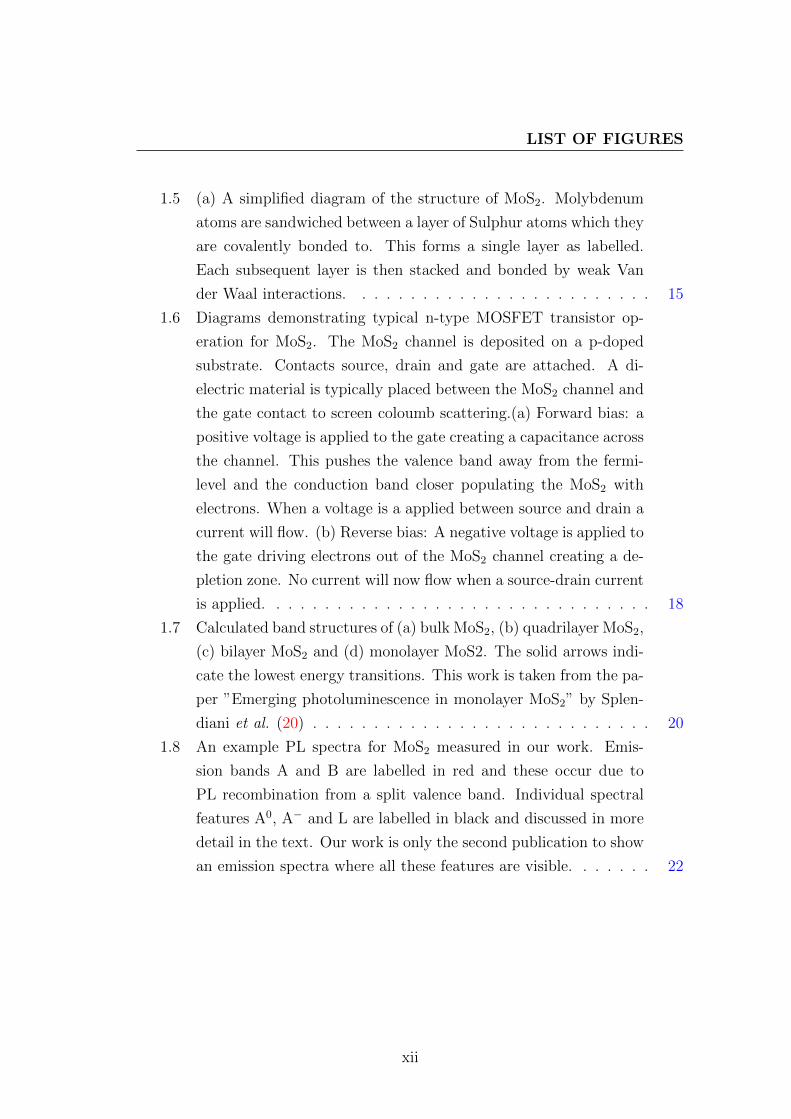
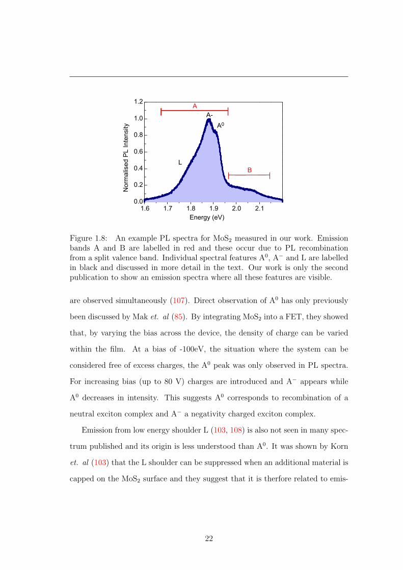
deposited on SiO2 capped Si substrates. A photoluminescence (PL) spectrum for
MoS2 measured in our work is provided in figure 1.8. Rather than a single peak,
the spectrum of MoS2 consists of two bands which are labelled as A and B in red.
This is a consistent observation in the literature and it has been shown (101, 105)
that these bands originate from emission from two distinct hole positions caused
by a splitting of the valence due to spin-orbit coupling at the K-point. These
two bands, A and B, are also detected in absorption spectra for bulk MoS2 (106).
The B peak has a much smaller intensity (∼15%) compared to the A peak in PL.
Looking at the spectra in figure 1.8 it can be seen that the A band is formed
from emission of different states labelled A0, A− and L on the diagram. The
observation of A0 and L varies significantly between publications and are often not
observed. There is, in fact, only one other published spectrum where both states
21
1.6 1.7 1.8 1.9 2.0 2.10.0
0.2
0.4
0.6
0.8
1.0
1.2
(
Nor
mal
ised
(PL(
Inte
nsity
L
A0
A-
B
A
Energy((eV)
Figure 1.8: An example PL spectra for MoS2 measured in our work. Emissionbands A and B are labelled in red and these occur due to PL recombinationfrom a split valence band. Individual spectral features A0, A− and L are labelledin black and discussed in more detail in the text. Our work is only the secondpublication to show an emission spectra where all these features are visible.
are observed simultaneously (107). Direct observation of A0 has only previously
been discussed by Mak et. al (85). By integrating MoS2 into a FET, they showed
that, by varying the bias across the device, the density of charge can be varied
within the film. At a bias of -100eV, the situation where the system can be
considered free of excess charges, the A0 peak was only observed in PL spectra.
For increasing bias (up to 80 V) charges are introduced and A− appears while
A0 decreases in intensity. This suggests A0 corresponds to recombination of a
neutral exciton complex and A− a negativity charged exciton complex.
Emission from low energy shoulder L (103, 108) is also not seen in many spec-
trum published and its origin is less understood than A0. It was shown by Korn
et. al (103) that the L shoulder can be suppressed when an additional material is
capped on the MoS2 surface and they suggest that it is therfore related to emis-
22
sion from surface states. Specifically they suggest that the L peak is emission
related to surface bound impurities, which would cause a localized perturbation
of the band-structure.
Polarization properties of PL emission from MoS2 has also proven interesting.
It has been shown experimentally that emission from MoS2 has the same degree
of circular polarization as the laser used for excitation, with results of up to 100%
helicity in selected experiments (85, 85, 87, 88, 108). This is interpreted that the
electrons in MoS2 can be optically addressed at the same position in energy, but
at different positions in k (momentum) space, known as valleys (85, 87, 88, 108).
Optically addressing momentum space therefore may provide yet another degree
of freedom for use in producing computational devices (86).
1.3.5 Our work on MoS2
In our work we develop a method for mechanical exfoliation of MoS2 onto Si/SiO2
substrates and we demonstrate PL emission for MoS2 sheets under 5ML in thick-
ness produced using our method. We find that there is a large variation in the
PL emission spectra shape between different samples, which can also be seen
in the literature (19, 20, 85, 103) but has not previously been highlighted. In
order to explain this we consider the effects of substrate interactions and also
the physical processes which determine the relative intensity of the different PL
emission features (A0, A−, L and B). Using atomic force microscopy (AFM), and
a specialised adaptation known as ultrasonic force microscopy (UFM), we present
unique images of defects which form in our MoS2 sheets during exfoliation.
In Chapter 4 we show that competition between radiative and non-radiative
23
processes effect the behaviour of PL with both temperature and incident power
dependence. We find further evidence to support previous results showing a low
quantum efficiency in MoS2 (80), finding that PL emission does not saturate
at high pumping powers. Importantly, we find that the dominant effect which
determines the variation in emission from states A−, A0 and L is the balance
of negative charge in the film. We show that negative state, A−, is dominant
for all spectra between 6.5-300K and provide evidence that this is formed due
to to charge capturing from the substrate. We find that electrons are thermally
activated in the SiO2 and show that, with increasing temperature, the relative
emission intensity of A0 and L decreases before disappearing.
In Chapter 5 we investigate how to control the charge balance in MoS2 and
therefore the PL line shape. Here we consider the effect of dielectric capping on
the PL properties and investigate MoS2 on substrates with different roughness.
We find, using AFM and UFM, that the addition of a capping layer increases
the mechanical bonding of the MoS2 with the substrate, which we find helps to
facilitate the charging process and creates a more stable charge balance in the film.
This is shown to lead to a suppression of states A0 and L. The effect of this is to
increase the uniformity of PL lineshape, emission energy and linewidth between
different samples and also to reduce linewidths. This work therefore provides
important results about substrate interactions as well as offering a potential way
to improve uniformity of electronic and optical properties of thin MoS2 sheets.
24
Chapter 2
Experimental Techniques
In the previous chapter we showed that integration of III-V semiconductor ma-
terials with Si electronics may be possible to achieve by growing NWs directly
on Si. In this thesis the electronic (optical) and structural properties of a novel
system of GaAs and GaAs/GaAsP NWs grown by catalyst free MBE are related
for the first time using complimentary techniques of continuous wave photolumi-
nescence (CW-PL), time resolved photoluminescence (TR-PL), scanning electron
microscopy (SEM) and transmission electron microscopy (TEM). We also intro-
duced MoS2, one of a new class of 2D materials which can be prepared similarly
to graphene. It has a bright PL spectra and can be used to make transistors.
In order to relate the electronic (optical) and structural properties of MoS2 the
complimentary techniques of CW-PL, atomic force microscopy (AFM) and ultra-
sonic force microscopy (UFM) are undertaken. In this chapter we introduce these
techniques individually and also give an introduction to photoluminescence.
25
2.1 An introduction to the principle of photo-
luminescence
excited state
ground state
relaxation
hωlaser injection
hole hole
electron
electron
Figure 2.1: Diagram of electron recombination demonstrating laser injection ofan electron-hole pair, relaxation of the electron to the minima of the conductionband and recombination resulting in the release of a photon of light.
Photoluminescence (PL) is a photon emission process due to the recombi-
nation of an optically created electron hole pair. For PL to occur in a semi-
conductor the absorption of a laser photon must promote an electron from the
valence band to the conduction band (27). For electron promotion to occur the
laser photon energy must be the same or higher than the material band-gap. All
experiments in this thesis were carried out using non-resonant above band-gap
excitation. The radiative recombination of the electron-hole pair may be preceded
by a non-radiative relaxation mechanism which leads to the emission of phonons.
26
Competition between non-radiative and radiative processes is important for both
our work on NWs and on MoS2.
E
k
E
k
Phononhω hωEg Eg
a) b) conduction band
valence band
conduction band
valence band
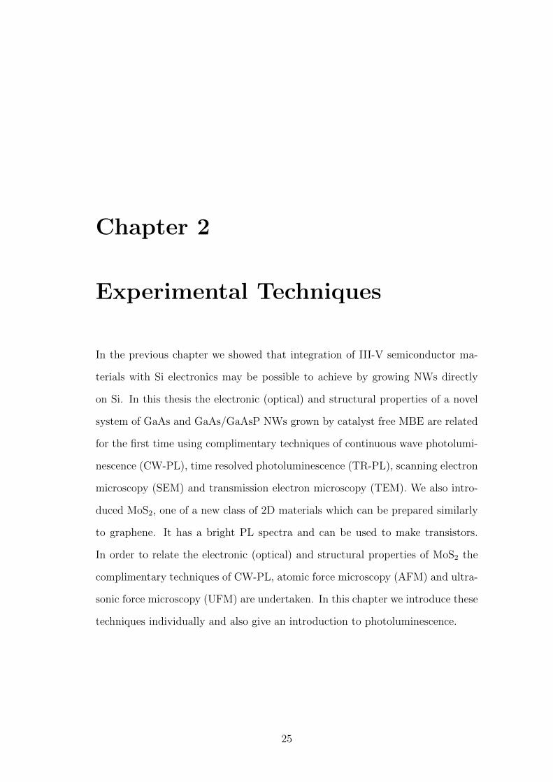
Figure 2.2: Diagrams showing the position of the conduction and valence bandminima in momentum space for direct and indirect band-gaps. In this case E isthe position in energy and k is the wavevector of the particle. (a) direct band-gaprecombination where the electron and hole have the same wavevector. (b) indirectband-gap recombination where the electron and hole have different wavevectorsand therefore require addition emission of a phonon before recombining.
Photo-excited electrons (holes) relax to the bottom of the conduction (valence)
band by emitting phonons (25). Optical recombination of electon-hole pairs oc-
curs at the energies close to the edge of the band-gap (12). If these band edges
occur at the same position of the Brillouin zone in momentum space (ie. have the
same wavevector) emission of a photon occurs with conservation of energy and
momentum without need for additional processes such as emission of phonons. If
they occur at different positions (ie. have different wavevectors), then emission
of a particle becomes a second order process and requires additional emission of
phonon in order to conserve momentum (26). This is therefore a slower process
and produces a lower emission rate of photons. The first order process is charac-
teristic to direct band-gap semiconductors and is found in the case of nanowires
and thin sheets of MoS2 studied in this thesis. Both processes are illustrated in
27
figure 2.2.
In an atom electrons sit in discrete energy levels and therefore produce a dis-
crete florescence emission spectra with line widths determined by the uncertainty
principle (109). In semiconductors the electrons and holes relax into the bottom
of the valence and conduction band respectively, forming a thermal distribution
before recombining (27). The line width of emission is related to this thermal
distribution KBT, where T is temperature and KB is the Boltzmann constant,
along with the density of states, carrier density and inhomogeneity of the crystal.
hω1 hω2hω3
Conduction Band
Valence Band
Figure 2.3: A diagram showing disorder in a bandgap created by localised strainon the relative position of atoms in a semiconductor. Arrowed lines in this caserespond to radiative recombination of an electron-hole pair and it can be seenthat different values of Eg will lead to a broadening of the spectra.
If confinement becomes great enough quantum effects can occur. In the case
of quantum wells and 2D materials such as MoS2, the electron is unrestricted in
movement in two directions, and confined in the third. This modifies the density
of states to a step like structure with each step corresponding to a confined
energy state (25). In the case of quantum wires, such as GaAs NWs, electrons
28
are confined in 2 directions. We find that the linewidth of emission from the
materials studied in this report are dominated by inhomogeneous broadening due
to structural disorder in our nanostructures. Localised strain on the atoms in a
crystal lattice effects their relative positions leading to a disordered band-edge
as demonstrated in figure 2.3. Radiative recombination of electron-hole pairs
(marked with arrows) will therefore have a slightly different energy at different
positions in the crystal.
2.1.1 Continuous wave photoluminescence
In our studies we focus on low temperature PL spectroscopy. A sample is placed
in vacuum on a cold finger in a He continuous flow cryostat as depicted in Figure
2.4b. Liquid He is pumped from a dewar into a series of copper tubes thermally
connected to the cold finger, causing the sample temperature to drop to 10K.
This system also allows temperature dependences to be measured.
Above band-gap excitation is achieved with the application of collimated laser
focused by a series of lenses as depicted in Figure 2.4a. The laser is focused onto
the sample using a microscope objective with a numerical aperture of 0.5 and
working distance of 13.6mm, a spot size of around 1.5µm is typically achieved.
These experiments can therefore be considered as micro-photoluminescence. In
order to prevent any broadband emission of the laser affecting the results, a
narrow pass filter is placed before the sample. A variable density filter can also
be used to control the incident laser power.
PL emission from the sample is collected through a series of lenses which focus
the signal on the entrance of the slit of a spectrometer. A long-pass filter placed
29
laser
lens line filter
variable denisty filter
cryostat
lenses
longpass filter
grating
CCD detection
vacuum pump
cold fingersample
He flow input
He flow output
b)
a)
PL
mirrors
grating
to power meter
beamsplitter
Figure 2.4: (a) A diagram showing the experimental setup for a standard PLexperiment where a focused laser beam is directed at a sample in a cryostat andPL emission is collected using a spectrometer and CCD. Here a neutral densityfilter is used to control the incident power of the laser and this is measured usinga power meter by splitting the beam. A line filter is used to remove broadbandemission from the laser and a long-pass filter placed before the spectrometerstops reflected laser light hitting the CCD. (b) A diagram of continuous flow Hecryostat. This is pumped so that the sample is in vacuum. A flow of liquid Hepasses through a series of copper pipes attached to a cold finger where the sampleis attached. This allows temperatures of 10K to be achieved.
in this path removes any reflected light from the incident laser. A diffraction
grating inside a spectrometer separates the incident PL by wavelength, which is
collected on a liquid nitrogen cooled charged coupled device (CCD) chip.
30
2.1.2 Time resolved photoluminescence
Time resolved PL is used to measure the temporal characteristics of light emission
as a result of sample excitation with a pulsed laser. Typically, the PL decays
in the nanosecond range in structures where the electron-hole pairs are tightly
bound (58). Instead of a continuous beam of photons, the sample is excited
by very short laser pulses, which are 2ps in the case of this work. The PL
spectrum is then recorded as a function of time from the arrival of the excitation
pulse. Resolution of the detector plays an important role in these experiments.
We use an avalanche photon detector (APD) in the case of samples with low
photon emission (uncapped GaAs NWs) and this had a 8meV spectral range (as
determined by the slit width) and temporal resolution of 350ps. For samples with
a higher photon yield and shorter lifetimes (capped GaAs/GaAsP NWs) we used
a streak camera that has an improved resolution of <5ps. This collects emission
in a single channel and therefore has a much lower sensitivity so could not be
used in the case of the uncapped GaAs sample.
31
2.2 Microscopy techniques used in this work
The optical properties of materials are heavily effected by their physical struc-
ture which can be studied using various microscopy techniques. In this thesis
atomic force and ultrasonic force microscopy is used to image 2D sheets of MoS2
and scanning electron and transmission electron microscopy is used to image
nanowires.
feedback loop
peizo stage
samplecantilever
photodiodelaser
atomic tip
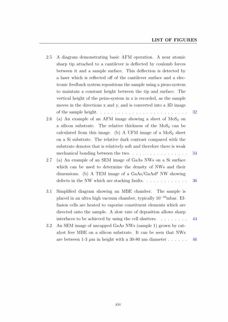
Figure 2.5: A diagram demonstrating basic AFM operation. A near atomicsharp tip attached to a cantilever is deflected by coulomb forces between it and asample surface. This deflection is detected by a laser which is reflected off of thecantilever surface and a electronic feedback system repositions the sample usinga piezo-system to maintain a constant height between the tip and surface. Thevertical height of the peizo-system in z is recorded, as the sample moves in thedirections x and y, and is converted into a 3D image of the sample height.
2.2.1 Atomic force microscopy
The atomic force microscope (AFM) was developed by Binning et. al. in 1986
(110), for which he received the Nobel Prize. This technique can be used to resolve
down to the atomic level. Atomic force microscopy (AFM) uses a sharp tip with
32
a radius of nanometre magnitude, which is attached to a cantilever. When the
tip is brought close to the sample surface, in the case of this work sheets of MoS2,
electrostatic forces act on the tip, which makes the cantilever bend according to
Hookes law. This force is detected by deflection of a laser against the cantilever,
into a photodiode detector. An electronic feedback detection system repositions
a piezo stage where the sample is held, which moves the sample up and down
keeping the tip at a constant height above the surface. This scheme is described
in figure 2.5 and was used in this work to measure the thickness of MoS2 samples.
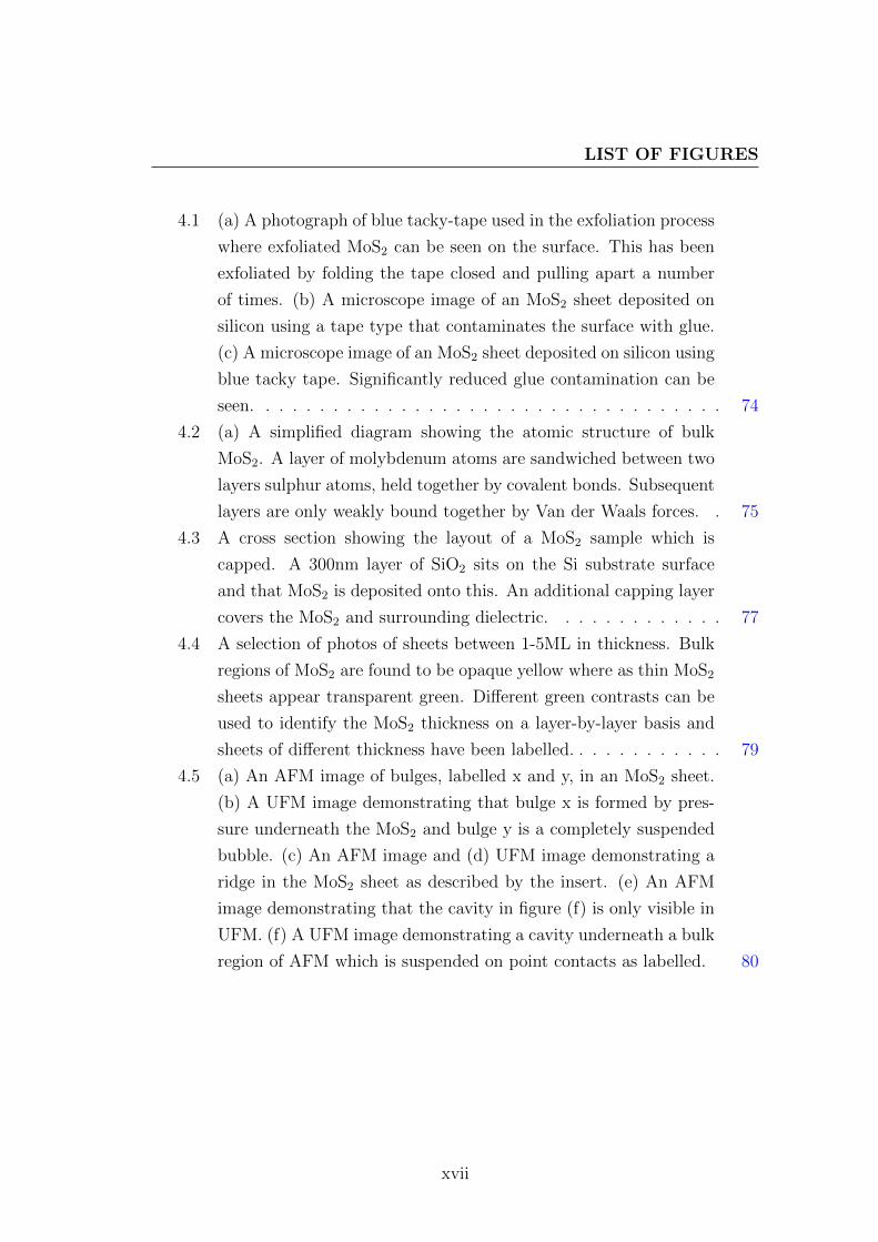
An example image of an MoS2 sheet on a Si substrate is given in figure 2.6a.
2.2.2 Ultrasonic force microscopy
Ultrasonic force microscopy was developed by Yamanaka et. al. in 1994 (111).
This adaptation of AFM can be used to measure stiffness of material (for exam-
ple mechanical coupling to the substrate) on the nanometer scale (112). For this
technique the sample is vibrated at small vibrational amplitude (0.5-2 nm) and
high frequency (2-10 MHz), much higher than the resonance frequencies of the
AFM cantilever. The restoring force of the sample is then modified by the stiff-
ness of the material, and this can be used to detect below-surface features such
as cavities, subsurface interfaces and sample-substrate interfaces. UFM can be
measured concurrently with AFM, detected on a separate channel where ultra-
sonic vibration at the tip-sample junction is converted into an image by nonlinear
rectification.
In this work UFM is used to detect nanometer scale resolution of stiffness of
2D structures of few atomic monolayer MoS2. An example UFM image of MoS2 is
33
(a)
MoS2 film
substrate (b)
Figure 2.6: (a) An example of an AFM image showing a sheet of MoS2 on asilicon substrate. The relative thickness of the MoS2 can be calculated from thisimage. (b) A UFM image of a MoS2 sheet on a Si substrate. The relative darkcontrast compared with the substrate denotes that is relatively soft and thereforethere is weak mechanical bonding between the two.
given in figure 2.6b. In this case bright (dark) colours correspond to higher(lower)
sample stiffness. This is used to detect below surface defects, regions of suspen-
sion and measure mechanical coupling of 2D materials with the substrate. In
particular, we use this technique to show weak mechanical bonding between the
substrate and MoS2 for free standing sheets and strong mechanical bonding when
a dielectric capping layer is added. Measurements of graphene using UFM have
been presented elsewhere (113).
2.2.3 Electron microscopy techniques
Diffraction limits the resolution of an optical microscope to around 1 µm. Elec-
trons have a small de Broglie wavelength, and therefore higher spatial resolution
can be achieved. There are two electron microscopy methods used in this the-
sis: scanning electron microscope (SEM) and transmission electron microscopy
(TEM).
34
2.2.3.1 Scanning electron microscopy
A sample is prepared using conductive glue to bridge between the sample and
sample holder, before being placed in a vacuum chamber. A focused beam of
electrons is produced thermoionically in a tungsten cathode and raster scanned
across the surface of the sample. Secondary electrons are emitted from the sample
due to inelastic scattering within a few nanometers of the surface (114). As
the angle of surface relative to the detector increases, the escape area of these
secondary electrons decreases and therefore the intensity drops. Electrons are
collected by a scintillator grid, which converts the intensity into an image. The
resolution of SEM is <1nm (115). In this work SEM is used to measure the
dimensions and density of GaAs NWs. An example SEM image is given in figure
2.7a.
2.2.3.2 Transmission electron microscope
Unlike SEM, where secondary electrons are emitted from the sample surface,
electrons in TEM are transmitted through the entire sample; usually after the
sample has been thinned to nm thickness. In experiments presented in this thesis,
the energy of electrons was set to 200kV. The electrons interact with atoms during
transmission and scattering can be used to produce an image (116). TEM has
a higher resolution compared to SEM as electrons are transmitted through the
crystal lattice, but requires samples to be extremely thin (<200nm) which is a
disadvantage for many systems (115). In the case of the NWs sample studied
here, the structure is already thin enough to be measured without any etching.
In order to isolate NWs for TEM measurements, a sample of wafer is cleaved,
35
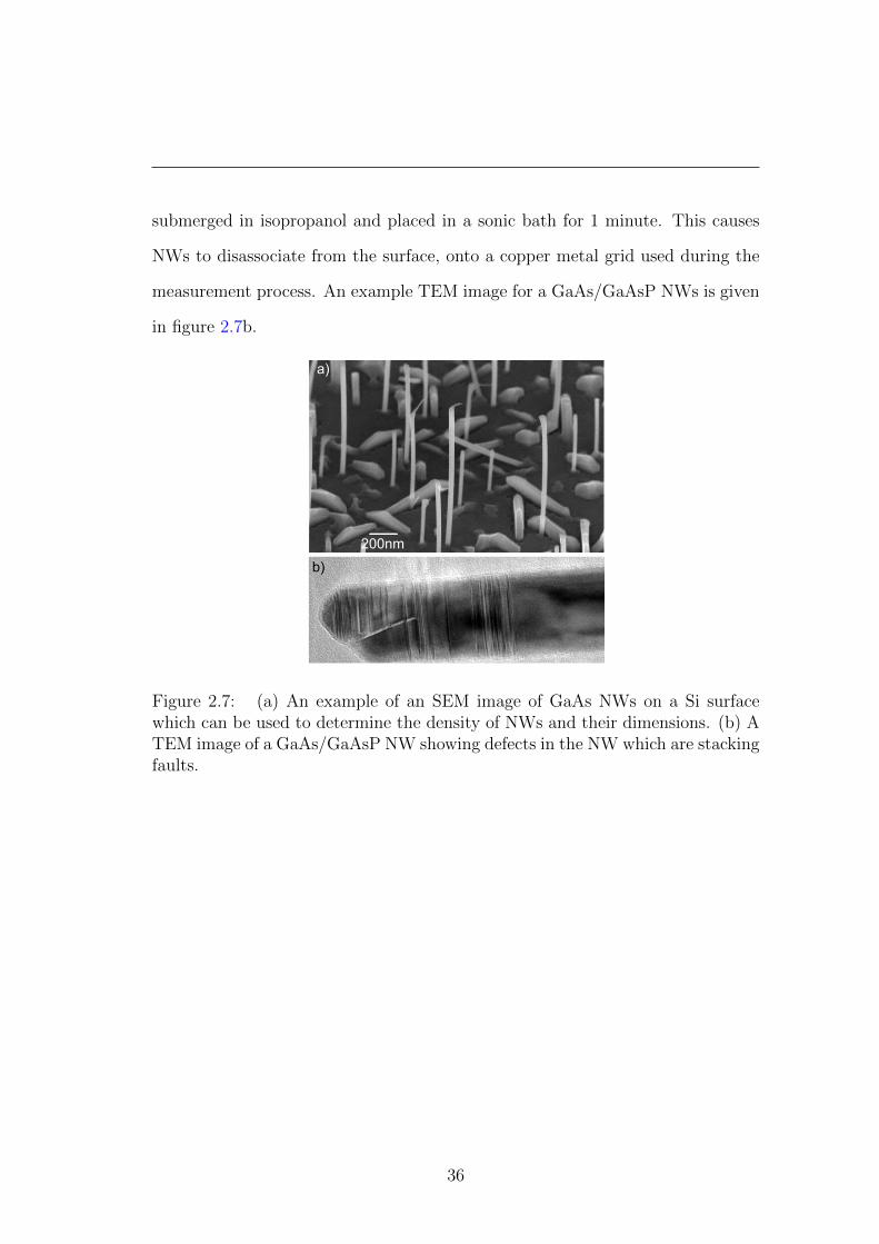
submerged in isopropanol and placed in a sonic bath for 1 minute. This causes
NWs to disassociate from the surface, onto a copper metal grid used during the
measurement process. An example TEM image for a GaAs/GaAsP NWs is given
in figure 2.7b.
200nm
a)
b)
Figure 2.7: (a) An example of an SEM image of GaAs NWs on a Si surfacewhich can be used to determine the density of NWs and their dimensions. (b) ATEM image of a GaAs/GaAsP NW showing defects in the NW which are stackingfaults.
36
2.3 Conclusion and remarks
Here we presented a selection of high resolution spectral, spatial and temporal
methods that were essential for this study. We performed CW-PL, TW-PL and
SEM at the University of Sheffield, UK. We performed AFM an UFM in col-
laboration with O. Kolosov and B. J. Robinson at the University of Lancaster,
UK. TEM measurements were performed for us by L. Otubo at the Instituto de
Pesquisas Energticas e Nucleares IPEN, Sao Paulo, Brazil
37
Chapter 3
Effect of GaAsP Shell on the
Optical Properties of
Self-Catalyzed GaAs Nanowires
Grown on Silicon
3.1 Introduction & Motivation
In section 1.2 we suggested that growth of nanowires (NW) may be the next step
in the integration of optical active III-V semiconductor materials with cheaper
Si electronics. In particular we highlighted addressing the specific need for cost
effective and efficient photovoltaics (43, 44, 44, 45, 46). Here we discuss NWs
grown on Si by a relatively new method which uses molecular beam epitaxy
(MBE), a method that is particularly advantageous as it is catalyst free, produces
a high crystalline quality and the density of crystal polytypes can be controlled
38
by varying the growth temperature (55, 56, 61).
III-V semiconductor NWs can be grown directly on Si as their narrow diam-
eter allows radial variations which relieve strain between the different material
structures without forming dislocations (22). By controlling the crystal phase
(wurtzite (WZ) or zinc-blende (ZB)), or creating hetrostructure quantum dots
by varying growth elements, electronic and optical properties can be controlled
by confinement (60, 61, 62, 117). Optical absorption of the solar spectrum, and
therefore efficiency of photovoltaic elements, can be maximised by accurately
controlling the NW width (45).
There are various effects which lead to broad photoluminescence (PL) emission
spectra in NWs which need to be considered in the case of our work. These include
crystal defects (stacking faults), inhomogeneity of the NW radius (118, 119) and
variations in strain within the capping layer in core-shell structures (58). Narrow
line-widths can be achieved by creating a heterostructure where an optically active
quantum dot (QD) is embedded in the NW length (36, 120, 121, 122). Embedding
QDs in a NW has the particular advantage that the QD dimensions can be
accurately controlled by both the NW diameter and the ability to create sharp
interfaces during growth (123). QDs embedded in NWs has particular use in
photonics, specifically in creating LEDs (22, 30, 31).
In our work we consider the effect of surface state recombination by compar-
ing capped and uncapped structures for the first time in NWs grown with this
method. Non-radiative exciton recombination on the surface of a semiconductor
material (63) reduces optical efficiency and this is particularly dominant for NWs
due to the large surface-to-volume ratio. The density of surface charge traps can
be greatly reduced by addition of a capping layer after growth of the NW, creating
39
a core-shell structure (65). The addition of a capping layer is often found to en-
hance optical emission yield (67) and its suggested that this is because it reduces
the density of non-radiative charge traps which exist on the NW surface (65).
Typical core-shell structures include catalyst free MBE grown GaAs/AlGaAs
Despite reports on their high crystal quality, few reports exist on the optical
properties of catalyst free MBE grown GaAs NW structures on Si, an issue we
address in this chapter. In particular we show the first ever measurements of
GaAs/GaAsP core-shell structures grown by this method. Growing NWs on
Si significantly reduces substrate costs and this catalyst free method avoids Au
contamination which may effect the efficiency of electron transport in photovoltaic
elements. In this work we consider photoluminescence (PL) from single NWs
to avoid the issue of inhomogeneities present in assembles, which allows clear
information on their properties to be gained. Optical measurements of single
self-catalysed NWs on Si are important for in-depth understanding and design of
electronic properties.
In particular we demonstrate that an improvement of optical properties of
these NWs can be achieved by addition of an MBE grown capping shell of GaAsP.
This leads to a dramatic increase in PL yeild of up to 2000x. So far no reports
have been published on MBE passivation of catalyst free NWs with GaAsP and
40
this may prove superior to materials such as AlGaAs (124) which are more prone
to oxidation and non-radiative surface states (66). By investigating thermal acti-
vation we are able to determine the main carrier escape mechanisms that lead to
PL quenching in the uncapped GaAs NWs. We show that a GaAsP capping layer
reduces the efficiency of comparable thermally activated non-radiative processes
in uncapped samples by 8 times. For this reason we find that GaAs NWs are
quenched at 60K but GaAs/GaAsP samples emit up to room temperature. We
link this quenching process to non-radiative recombination on the NW surface and
show that GaAs PL yield degrades significantly over time due to oxidation of the
surface. We find a second high energy PL quenching process for the GaAs/GaAsP
sample which we relate to electrons escaping from the GaAs core into the GaAsP
shell.
Considering TEM measurements we find that our GaAs/GaAsP core-shell
NWs have a high crystal quality which is dominated by the GaAs zinc-blende
phase. By linking the crystal structure to observations of PL, we find type-
II quantum confinement in the case of our uncapped GaAs NWs which were
grown at a lower temperature. In this case electrons and holes are spatially
separated in different crystal phase poltypes. We show that holes are confined in
wurtzite segments and electrons in zinc-blende segments. We also suggest that
the band-gap of emission can be strain-tuned in our NWs by alternating the
nominal concentration of P in a GaAsP capping shell.
We therefore demonstrate that GaAs NWs grown on Si using the catalyst
free MBE technique are a high quality material with robust optical properties
for potential use in highly efficient photovoltaic elements. We show that the
optical and electronic properties can be effected by selective control of structural
41
properties during growth.
42
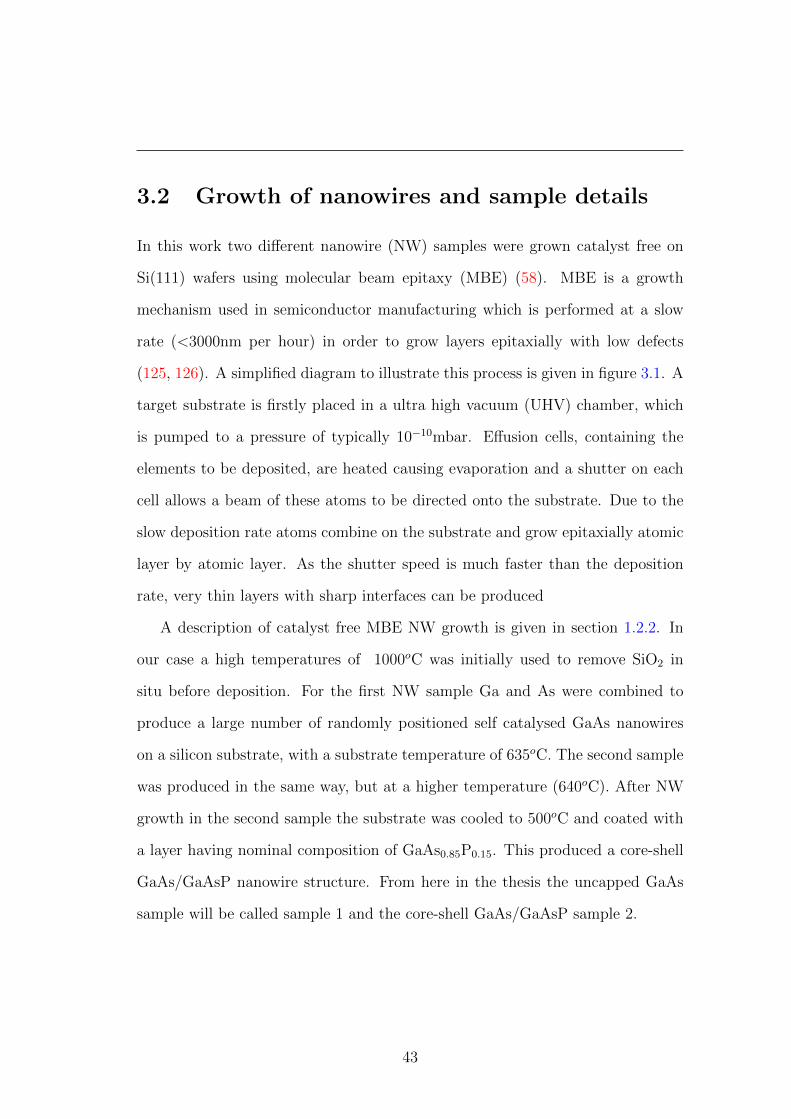
3.2 Growth of nanowires and sample details
In this work two different nanowire (NW) samples were grown catalyst free on
Si(111) wafers using molecular beam epitaxy (MBE) (58). MBE is a growth
mechanism used in semiconductor manufacturing which is performed at a slow
rate (<3000nm per hour) in order to grow layers epitaxially with low defects
(125, 126). A simplified diagram to illustrate this process is given in figure 3.1. A
target substrate is firstly placed in a ultra high vacuum (UHV) chamber, which
is pumped to a pressure of typically 10−10mbar. Effusion cells, containing the
elements to be deposited, are heated causing evaporation and a shutter on each
cell allows a beam of these atoms to be directed onto the substrate. Due to the
slow deposition rate atoms combine on the substrate and grow epitaxially atomic
layer by atomic layer. As the shutter speed is much faster than the deposition
rate, very thin layers with sharp interfaces can be produced
A description of catalyst free MBE NW growth is given in section 1.2.2. In
our case a high temperatures of 1000oC was initially used to remove SiO2 in
situ before deposition. For the first NW sample Ga and As were combined to
produce a large number of randomly positioned self catalysed GaAs nanowires
on a silicon substrate, with a substrate temperature of 635oC. The second sample
was produced in the same way, but at a higher temperature (640oC). After NW
growth in the second sample the substrate was cooled to 500oC and coated with
a layer having nominal composition of GaAs0.85P0.15. This produced a core-shell
GaAs/GaAsP nanowire structure. From here in the thesis the uncapped GaAs
sample will be called sample 1 and the core-shell GaAs/GaAsP sample 2.
43
Effusion Cell
Effusion Cell
Effusion Cell
Effusion Cell
Cell shutter
Principal shutter
Sample holder
Rotation Arm
UHV (ultra high vacuum)chamber
Figure 3.1: Simplified diagram showing an MBE chamber. The sample is placedin an ultra high vacuum chamber, typically 10−10mbar. Effusion cells are heatedto vaporise constituent elements which are directed onto the sample. A slow rateof deposition allows sharp interfaces to be achieved by using the cell shutters.
44
3.3 Microscopy characterization
In this section measurements using Scanning Electron Microscopy (SEM) and
Transition Electron Microscopy (TEM) are presented to describe the structural
properties of the NW samples. We therefore demonstrate that we have high
quality crystalline samples, similar in quality to those previously reported (55, 56).
In order to isolate NWs for TEM measurements, a sample of wafer is cleaved,
submerged in isopropanol and placed in a sonic bath for 1 minute. This causes
NWs to disassociate from the surface, onto a copper metal grid used during the
measurement process. TEM measurements were not performed for the uncapped
Sample 1 as it was found that when trying to remove NWs they collapsed and
stuck strongly to the substrate. A complex structure of WZ/ZB phase defects
can be detected in PL measurements presented in this chapter.
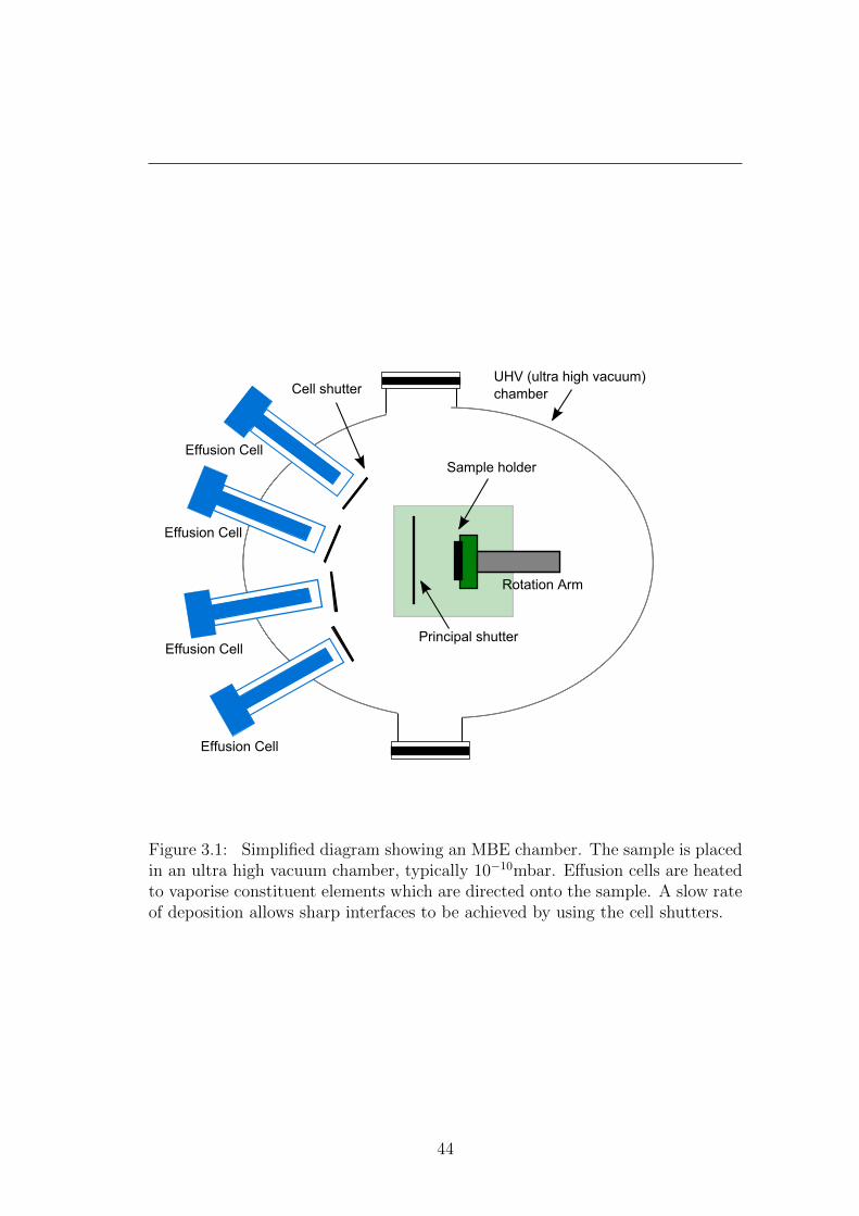
3.3.1 GaAs NWs (Sample 1)
An SEM image of GaAs NWs is given in figure 3.2. It is found that by varying the
position across the growth wafer from the centre to the edge, the density of NWs
decreased outwards. The density at the centre of the sample is ∼ 10NW/µm2
and the edge <0.5NW/µm2. The SEM image provided is from a relatively high
density part of the sample. It can be seen that NWs are well isolated and vertically
standing on the surface. These NWs are between 1-3 µm in height and 30-80 nm
in width. In order to carry out µ-PL measurements a position on the sample is
chosen with a low enough density to successfully isolate a single NW.
45
1μm
Figure 3.2: An SEM image of uncapped GaAs NWs (sample 1) grown by catalystfree MBE on a silicon substrate. It can be seen that NWs are between 1-3 µm inheight with a 30-80 nm diameter
3.3.2 GaAs/GaAsP NWs (Sample2)
An SEM image of the GaAS/GaAsP sample is provided in figure 3.3a. NWs are
again found to be well isolated and decreasing in density from centre to wafer
edge, although the higher density section of the wafer is of a lower density than
the previous sample (∼1.5 µm2). The height of NWs on this sample is again
found to be between 1-3 µm. The diameters are found to be greater than the
previous sample (between 50-120 nm), which is expected due to the additional
capping layer. To measure the crystal structure and nominal thickness of the
GaAsP layer we carried out TEM measurements.
TEM images of these GaAs/GaAsP NWs were possible to measure as we were
able to remove NWs from the substrate in this sample. Using image contrast in
figure 3.3b it is possible to measure the width of the GaAs core to be 30nm (upto
46
70nm in other samples), similar to the width of the uncapped NWs. The diameter
of the NW is shown to be very uniform along its length. The nominal thickness
of GaAsP layer is found to be 10nm.
As described in section 1.2.3 both wurtzite (WZ) and zinc-blend (ZB) polytype
lattice structures are possible in NWs. An electron diffraction spot pattern for
the GaAs/GaAsP NWs is given in figure 3.3d. This was collected in addition to
TEM by detecting Bragg scattered electrons, which were detected in the back-
focal plane (rather than the standard focal plane used for imaging). This exploits
diffraction effects of electrons and each diffraction spot denotes a plane of atoms
within the atomic crystal. In order to analyse this image detailed fast Fourier
transform analysis were carried out for us which utilised the interpretation of
Sarney et. al (127). This diffraction measurement confirms that these NWs are
ZB in structure. We found that all NWs in this sample were in fact ZB.
Defects at the tip of the GaAs/GaAsP NWs can be seen in figure 3.3c. It
is possible to identify some of these as twinning of the ZB crystal plane (128).
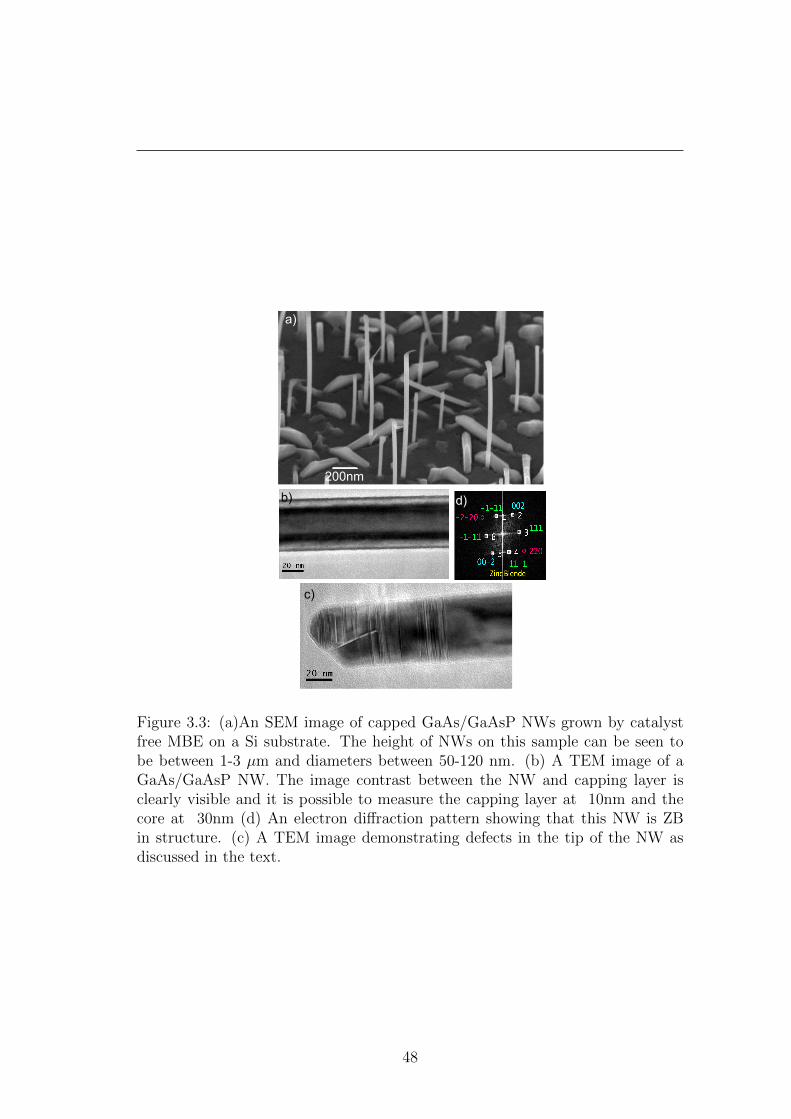
This is shown in more detail in figure 3.4b and this occurs due to stacking faults.
The stacking order of ZB is ABCABC and these stacking faults occur in the
form of a ABCACBA sequence (22). In rarer cases a NW where a wurtzite
(WZ) stacked GaAs region interjects between ZB stacked layers was found (60)
as demonstrated in figure 3.4a. This defect was only observed in a small number
of NWs. All defects found were small and isolated in the NWs tip, therefore the
GaAs/GaAsP NWs presented in this report can be considered as high quality ZB
structures.
47
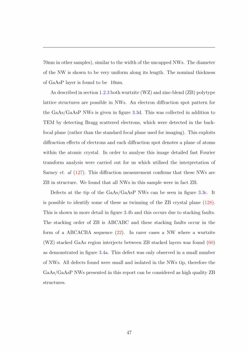
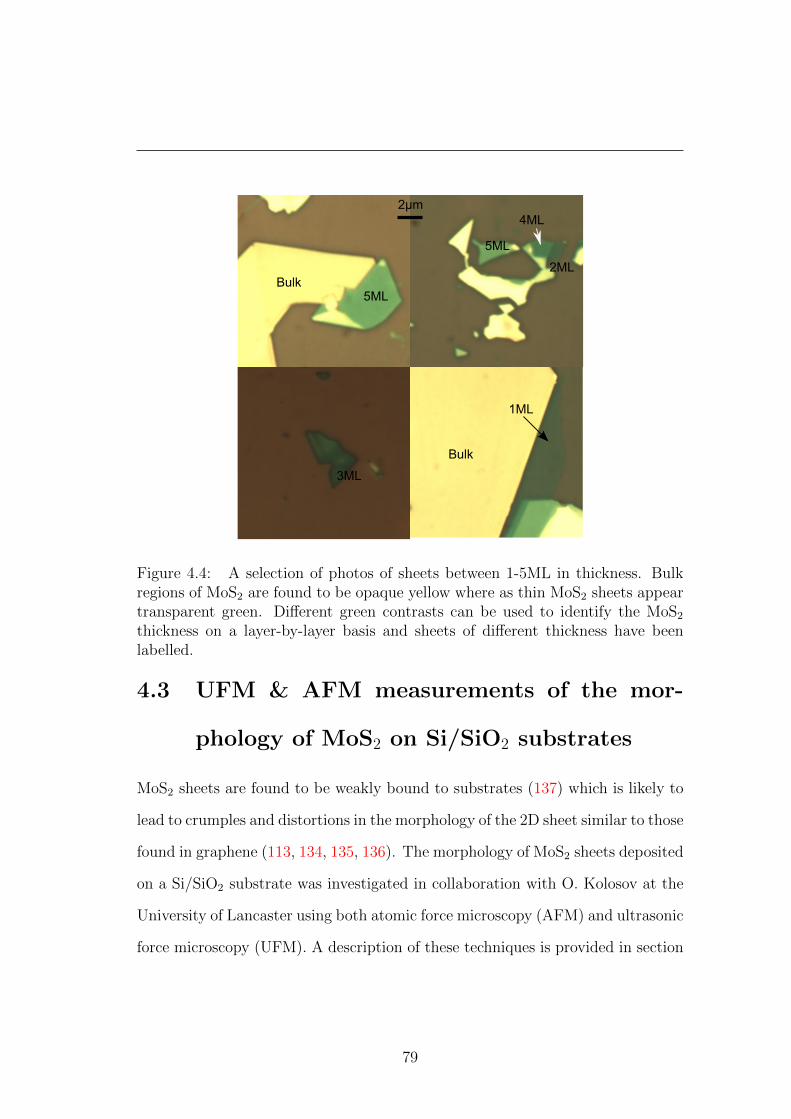
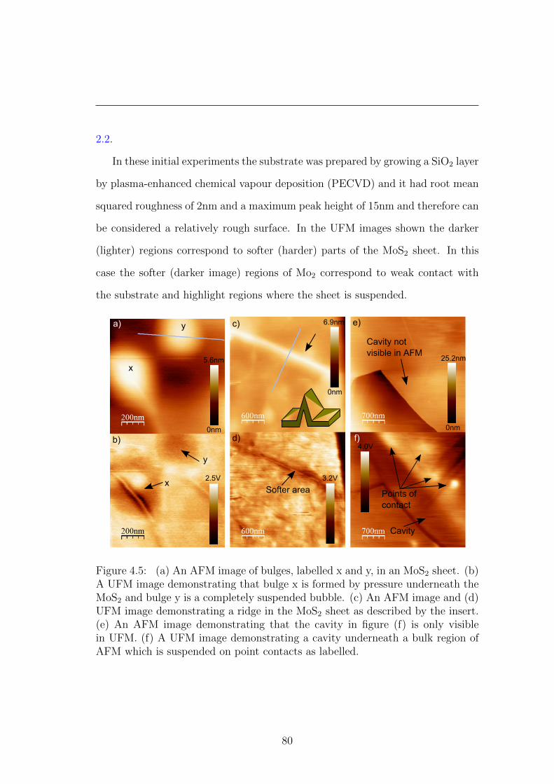
200nm
a)
b) d)
c)
Figure 3.3: (a)An SEM image of capped GaAs/GaAsP NWs grown by catalystfree MBE on a Si substrate. The height of NWs on this sample can be seen tobe between 1-3 µm and diameters between 50-120 nm. (b) A TEM image of aGaAs/GaAsP NW. The image contrast between the NW and capping layer isclearly visible and it is possible to measure the capping layer at 10nm and thecore at 30nm (d) An electron diffraction pattern showing that this NW is ZBin structure. (c) A TEM image demonstrating defects in the tip of the NW asdiscussed in the text.
48
a)
Stacking faults
Zinc-blendeWurtzite
Figure 3.4: (a) A TEM image showing the rare case where a section of WZstacked GaAs crystal interjects into the NW at the tip forming WZ/ZB stackingsections. (b) A TEM image showing defects due to stacking sequence faults inthe ZB cyrstal at the tip of a GaAs/GaAsP NW as described in the text.
49
3.4 Optical PL measurements
Continuous wave (cw) optical measurements of NWs are carried out with a 1.893
eV diode laser focused on the sample with a 1.5µm sized region. The sample was
placed in a vacuum cryostat with variable temperature. PL measurements were
collected from above the NWs with a spot size of 1.5µm . A single spectrometer
was used for all measurements as high resolution was not required.
Further to CW-PL measurements, time resolved PL spectra are also collected.
For the uncapped GaAs NWs the data was collected using an avalanche photo-
diode (APD) with a resolution of 350ps and data for the GaAs/GaAsP NWs
collected using a streak camera with a resolution of 5ps. For these measurements
excitation was achieved using a Ti-sapphire laser producing a series of 2ps pulses.
The laser excitation for uncapped samples was 1.595eV and for GaAs/GaAsP
samples 1.71eV. All measurements were performed at 10K temperatures.
3.4.1 GaAs NWs (Sample 1)
3.4.1.1 Continuous wave PL measurements
A selection of PL spectra for the uncapped GaAs NW sample is presented in
figure 3.5. These spectra are collected with an excitation power of 100µW and
a collection time of 10s. It can be seen that emission from this sample has a
relatively narrow linewidth (between 5-20meV) and a very large emission range
of 100meV, with emission visible below the band-gap of GaAs (1.52eV (59)).
By moving the laser focus on a single NW different positions along the length
could be excited. It was found that, for different positions along the NW length,
emission was detected at different energies. Multiple NWs were considered to
50
achieve the total range in figure 3.5
1.40 1.42 1.44 1.46 1.48 1.50 1.52 1.540
1000
2000
3000
4000
d
d
Energyd(eV)
PLd
coun
ts
EgWZ
EgZB
e
h
WZZB
WZ
growthddirection
a)
b)
ZBZB/WZ
115meV
Figure 3.5: (a)A PL spectrum of various GaAs NWs measured at 100µW witha collection time of 10s. This demonstrates PL emission for the whole range de-tected, with both type II (emission confined between ZB and WZ layers) and typeI emission (from ZB) sections labelled. (b) A diagram demonstrating quantumconfinement of electrons and holes in the NW growth direction which leads totype II spatial confinement.
In order to explain below the band-gap emission energies, the structure of the
NW must be taken into account. The bandgap of ZB is EZBg =1.515 (59) and the
bandgap of WZ has been measured between EWZg =1.5 - 1.58eV (129). The fact
that emission is found below this, up to ∼1.405eV, suggests an effect of crystal
phase electron confinement between the two crystal types. This has previously
51
been observed in III-V NWs grown by different methods (61, 62, 64, 117, 128).
In this case holes are expected to be confined in the maxima of the valence
band of WZ segments and electrons confined in the conduction band of the ZB
segments. This special case of confinement, described as type II, is presented
diagrammatically in figure 3.5b.
The lowest emission measured, 1.405eV, reflects a valence band offset between
ZB and WZ structures of 115meV; which agrees well with previously calculated
results (47, 60). This is expected to arise from e-h recombination, as demonstrated
in figure 3.5b, at the boundary between large ZB and WZ segments and has the
largest confinement. The wide range of emission energies observed in our studies
arises from variation of the thicknesses of the WZ and ZB segments, leading to
variation of the carrier confinement. As the confinement becomes weaker emission
energy increases. Emission at 1.514eV, the highest energy measured, is expected
to be type I emission from single phase WZ GaAs.
3.4.1.2 Time-resolved PL measurements
This conclusion is further supported by time resolved PL measurements per-
formed on different GaAs NWs emitting across the whole range of emission ener-
gies, and at different points along a NW spectrum. In Figure 3.6a a PL spectra
for a single NW which is expected to have type II confinement is presented. In
figure 3.6b decay curves of relative emission intensity with time, collected using
an APD, are presented for the different positions marked on the above diagram.
To find the decay constant τ , the decay of emission energy was fit to a single
exponential function in equation 3.1.
52
I = I0e− tτ (3.1)
1.40 1.42 1.44 1.460
500
1000
1500
i
PLi
coun
ts
Energyi(eV)
- 1 1 2 3 4 5 6 7 8
0.1
0 2 4 6 8ΔTi(ns)
7.4ns
2.4ns
4.1ns
0
1
Nor
mal
ised
iPlii
nten
sity
Figure 3.6: (a) A PL spectrum of the single GaAs NW emitting below thebandgap of ZB GaAs. The position in energy considered for time resolved analysisis marked with arrows. (b) Time response measured using a APD at Pex = 20 Wfor a single NW in the positions indicated by arrows in the spectrum in part (a).
A value of τ=7.4 ns is measured for NWs emitting at lower energies of 1.425eV.
This long lifetime is characteristic of indirect exciton recombination (type II) due
to the relatively large spacial separation between electrons and holes localised in
regions with different crystal phases. A shortening of the lifetime for emission
53
is observed when we compare NWs emitting at higher energies. This shortening
of the lifetime (with increasing energy) reflects stronger overlap between electron
and hole. This is due to the carrier confinement becoming weaker as the size
of relative WZ segments are reduced. For the highest emission energy detected
(1.52ev) the lifetime is only 0.3ns (the resolution of the experiment) and this
corresponds to type-I alignment (emission of a pure ZB phase) (130). Additional
lifetime shortening (as observed directly in the figure 3.8) may be related to
contribution of carrier escape to faster non-radiative surface states.
3.4.2 GaAs/GaAsP NWs (sample 2)
3.4.2.1 Continuous wave PL measurements
Figure 3.7 shows emission spectra from individual core-shell GaAs/GaAsP NWs.
This was collected with an excitation power of 100 nW and collection time of
5s. Unlike uncapped GaAs NWs, there is no local variation in the observed peak
position. The lack of variation can be compared with observations of crystal
structure detailed in section 3.3. Using TEM we found that the crystal structure
of the NW is purely ZB, with few defects, and therefore type II confinement can
not occur. The emission is therefore from direct (type I) recombination of the
bandgap of ZB GaAs, as depicted in figure 3.7b. Type-II confinement is also not
observed between the NW core and shell. This is because the excitons are largely
confined in the NW core as is described in the next section.
The emission energy of these samples, 1.57eV, is much higher than the ZB
band-gap of 1.52eV. This blue shift is the result of strain imparted on the NWs by
the capping layer due to lattice mismatch. In this case the band-gap is changed
54
by pushing atoms closer together. The addition of 15% P concentration in GaAsP
(as used in these samples) has been predicted in other work (69) to lead to a blue
shift of 50meV, which is consistent with our work.
Due to the process of MBE deposition, there is expected to be a small variation
in thickness of capping layer and concentration of P over the sample. While this
effect is reduced by rotating the sample during growth, a small variation is still
expected which explains a slight variation in emission energy over the sample
surface. The linewidth of emission is 50meV, much larger than the previous
sample. This will be considered in the next section.
1.45 1.50 1.55 1.60 1.65 1.700
2500
5000
7500
b
b
Energyb(eV)
PLb
inte
nsity
EgGaAs
EgGaAsP
Gro
wth
bdire
ctio
n
e
h
a)
b)
Figure 3.7: (a) PL spectrum of various GaAsP/GaAs NWs which show only asmall variation in the emission energy and a linewidth of 50meV. (b) A diagramdemonstrating type I confinement where an exciton recombines down the NWlength.
55
3.4.2.2 Time-resolved PL measurements
Figure 3.8 demonstrates a PL spectrum (insert) and decay curve collected using
a streak camera (a) for a single core-shell GaAs/GaAsP NW. Carrier lifetimes in
this case are measured to be around 1.43ns, which is similar to lifetimes of type-I
self assembled quantum dots where the excitons are typically localised on the
length scales smaller than the Bohr radii in bulk material (4, 58). This implies
that the PL signal detected originates from excitons which are tightly bound
within the NW.
0 5 0 0 1 0 0 0 1 5 0 00 500 1000 1500
time (ps)
1.43ns
1.59 1.62 1.65E (eV)
a)
b)
Figure 3.8: PL time evolution for a single GaAs/GaAsP NW evaluated at theenergy of 1.6295 eV (solid line corresponds to exponential decay fit). The insetshows the PL intensity accumulated over a time window of 1.7 ns after pulsedlaser excitation at time 0.
56
3.4.3 Comparison of emission spectra GaAs and GaAs/GaAsP
NWs
An illustrative comparison of optical properties of GaAs and GaAs/GaAsP NWs
is given in figure 3.9. The line-width of the PL emission from GaAs/GaAsP is
found to be between 20 and 50meV - much larger than the emission of uncapped
GaAs NWs which was between 5-20meV. Despite this, even the largest linewidth
is still much smaller than the overall spread of PL peaks in the uncapped sample,
which is 100meV due to type II confinement. The larger linewidth for individual
peaks of GaAs/GaAsP NWs is likely related to the radial confinement potential
variations which appear due to strain inhomogeneities in the capping layer.
An impressive increase in emission yield when comparing with the GaAs and
GaAs/GaAsP samples can be seen in figure 3.9. The enhancement is on average
∼2000x, with increases up to 20000x being observed when comparing the weakest
emission of uncapped NWs and the brightest emission of GaAs/GaAsP NWs.
This is a much higher increase than in previously measured core-shell NW systems
(54, 67).
This enhancement of PL emission can be related to the passivation of the outer
layer by the addition of GaAsP capping. NWs naturally have a large surface to
volume ratio, and therefore surface states play an import role in determining
emission properties as they can act as paths for non-radiative recombination.
The intensity of PL is therefore partially determined by competition between
these surface states and radiative emission.
Work on temperature dependence presented below demonstrates that in capped
structures the electrons are strongly confined within the core and therefore will
57
1.35 1.40 1.45 1.50 1.55 1.60 1.65 1.70 1.75 1.80
m
m
Em(eV)
PLm
(arb
.muni
ts)
GaAsGaAs/GaAsP
Integrationmtimem1s
x100(Integrationmtimem60s)
Figure 3.9: Comparison of emission intensity and linewidth between uncappedGaAs structures on sample 1 and GaAs/GaAsP core-shell NWs on sample 2. Itcan be seen that the GaAs/GaAsP core-shell structure has an enhanced PL yieldas well as a much broader linewidth - 50meV compared to 10meV.
be isolated from the surface. This is further confirmed as we do not observe PL
corresponding the the GaAsP shell. An increased isolation of electrons from the
surface due to increased confinement is therefore likely to be the dominant effect
in reducing the effect of surface states and enhancing emission yield for capped
structures. Additionally, the capping layer may also act to suppress charge traps
at the surface (54, 65, 67). This is the first time that PL enhancement has been
measured for GaAsP capping on NWs grown by catalyst free MBE. GaAsP in
this case was chosen as it is less prone to oxidation (124) than AlGaAs (64, 65).
58
1.35 1.40 1.45 1.50 1.550
300
600
900
PL
inte
nsity
Energy (eV)
NW
After NH3 treatment
Figure 3.10: PL spectra demonstrating a uncapped GaAs NW (sample 1) whichhas been allowed to oxidise naturally over time (in red). It can be seen thatadditionally to NW emission at 1.47 a broader lower energy shoulder has appearedwhich we attribute to oxygen impurities. We also demonstrate (in black) thatthe PL yield of NWs can be enhanced, and simultaneous the low energy peakremoved, by washing the sample in NH3.
3.4.4 The effect of oxidization on surface states of un-
capped GaAs NWs
Further confirmation of the effect of surface states in uncapped NWs is provided
by measuring how the PL intensity of this sample degrades over time. The
addition of a capping layer acts to protect the NWs from interactions with their
environment. For an uncapped sample which was stored in air, a reduction of PL
intensity is found to be dramatic over a time scale of weeks and simultaneously
to this a second and much broader (70-130meV) peak appears at 1.4 eV (figure
3.10). As NWs have a large surface to volume ratio, oxidation of the outer
layers will effect its properties and oxidation has previously been observed on
the surface of bulk GaAs (131). We therefore ascribe this low energy peak to
oxygen impurities and this oxidation process creates additional surface traps.
59
The oxidation process is found to increase in speed when the sample is thermo-
cycled during measurements and can occur on a timescale of hours. Conversely
core-shell GaAs/GaAsP NWs do not degrade noticeably over time.
Surprisingly it was found that this degradation process can be reversed by
washing the sample in ammonia (NH3) dissolved in water and we must assume the
acid dissolves and washes away these impurities from the NW surface. The result
of this is given in figure 3.10 and it can be seen that by removing oxide surface
states the NW emission becomes brighter. Both these observations highlight
the detrimental effect surface states play on the intensity of PL and support
the suggestion that enhancement of PL by capping is due to the suppression of
(non-radiative) surface states.
60
3.5 PL power dependence of GaAs and GaAs/GaAsP
NWs
In order to see how the optical properties of the NW samples changes with incident
photon intensity, PL power dependence was studied. Figure 3.11a shows PL
spectra measured at a series of incident power (Pex) between 5µW and 200µW
for uncapped GaAs NWs. At very low values of Pex, only two peaks (labelled E1
and E2) are detected at 1.4625 and 1.4677 eV respectively. As Pex increases the
intensity of E2 becomes higher than E1 which quickly saturates with increasing
power. At the same time, new peaks (E3 and E4) appear on the higher energy
side of E2, eventually becoming brighter than the latter with further increases in
Pex. All 4 peaks blue shift with power as a consequence of band bending effects
at the type-II WZ/ZB interface (67).
The power dependence shown in figure 3.11a is, therefore, a clear signature
of the state filling effect on a single GaAs NW. By fitting the spectra collected
at 50µW with 3 Lorentzian curves, the splittings between adjacent states are
∆E21=E2-E1=5.2 meV and ∆E32=4.5 meV. This is related to the localisation
length of electrons. For example we can use the energy level solution for an
infinite square well potential (25):
En =n2h2
8µL2(3.2)
Where E is energy, h planks constant, µ the effective mass, L the confinement
length and n=1,2,3,4. We use the simplification that the nanowire length is
infinite and the effective mass for GaAs used is 0.067me (26). Considering a value
61
PLW
inte
nsity
EnergyW(eV)
PLW
inte
nsity
EnergyW(eV)
GaAs/GaAsPW
b)
1.46 1.47 1.48 1.490
3000
6000
9000
12000
E4
E3
E1
W
W
Pex
( W)
510255090150200
E2
a)
1.55 1.56 1.57 1.58 1.59 1.60 1.61 1.620
10000
20000
30000
40000 Pex
W(nW)
205010050010002000
W
W
GaAs
Figure 3.11: (a) Emission uncapped GaAs NWs (sample 1) with varied incidentpower. It can be seen that with increasing energy, additional states are filledwhich have been labelled E1-E4 (b) Emission from capped GaAs/GaAsP NWs(sample 2) with varied incident power. State filling can be similarly observed butthe linewidth of individual states are much larger.
of E21=5.2meV we calculate a confinement length of 57nm. This is consistent
with the NW radius measured in SEM and we therefore attribute the splitting
of the emission band into 4 well-defined peaks to radial confinement associated
with the NW width.
Figure 3.11b shows a power dependence from a single GaAs/GaAsP NW. As
for uncapped NWs, we observe the state filling effect. In this case the spectra
is much broader and individual states are approximately twice larger than what
62
we have presented in figure 3.11a for an uncapped NW. This broadening is again
likely to be related to inhomogeneity in strain related to the GaAsP capping
layer.
3.6 PL temperature dependence of GaAs and
GaAs/GaAsP NWs
In the above work it was observed that the addition of a GaAsP capping layer to
the GaAs NWs leads to a large enhancement of the PL yield. As discussed, sim-
ilar results have been published for different NWs and capping materials and it
is often explained that the capping layer acts to suppress non-radiative recombi-
nation paths at the NW surface. In order to understand in more detail the effect
of PL quenching mechanisms comparing capped and uncapped NW samples, a
series of detailed temperature dependent measurements are collected. These were
performed between 10K and room temperature (300K).
A comparison of relative PL intensity as a function of temperature for both
GaAs/GaAsP NWs and GaAs NWs is given in figure 3.12. The intensity of GaAs
NWs is found to drop quickly with temperature, where as GaAs/GaAsP NWs
are still visible at room temperature. These results are modelled using the dual
activation equation (132) for capped GaAs/GaAsP NWs:
IPL(T )
I0=
1
1 + A1exp(−E1/KBT ) + A2exp(−E2/KBT )(3.3)
and a single activation for uncapped GaAs NWs:
63
IPL(T )
I02=
1
1 + A12exp(−E12/KBT )(3.4)
Where I01 and I02 are the normalization constants, E1 (E12) and E2 are the
activation energies of PL quenching processes as describe below, A1 (A12) and
A2 characterize the efficiencies of non-radiative processes (as related to E1 (E12)
and E2) and KB is the Boltzmann constant. A simplified equation for uncapped
GaAs NWs was chosen due to the limited temperature range of emission.
0.00 0.03 0.06 0.09 0.12 0.1510-3
10-2
10-1
100
K
K
PLK
Inte
nsity
K(N
orm
aliz
ed)
1/TK(K-1)
Figure 3.12: Temperature dependence of normalized PL for GaAs (squares) andGaAs/GaAsP (circles) single NWs. Lines represent fit to data as explained inthe text.
Values of extracted parameters are given in table 3.1. The process E1 (E12)
is likely associated with the activation of non-radiative recombination centres at
the GaAs surface. While activation energy E1 (E12) is similar for both GaAs and
GaAs/GaAsP NWs, the value of A12 is approximately 8 times smaller for the
passivated GaAs/GaAsP NWs than A1 for the uncapped GaAs NWs; showing
that the efficiency of this process is reduced by capping. We therefore suggest
64
that the enhanced PL in the case of core-shell structures is due to a favourable
change in the balance of efficiencies between radiative and non-radiative processes.
This is most likely a consequence of stronger confinement of electrons in the
core of GaAs due to the GaAsP shell compared to GaAs with an open surface
(65, 66, 67, 67). We can estimate this strong confinement in core shell structures
by considering the PL quenching mechanism E2 below.
In the case of the capped GaAs/GaAsP NWs PL is observed up to room
temperature. The intensity of PL emission for these capped structures is in fact
brighter at 300K than the uncapped GaAs NWs at 6k. A second PL quenching
mechanism, where E2=48meV, is seen in this sample and found to have a large
efficiency at high temperature. It is possible to associate this process with car-
rier escape from the GaAs NW core to the GaAsP barrier. This occurs when
electrons confined in the core are thermally activated and able to escape over
the energy barrier. The conduction and valence band confinement potentials
for the GaAs/GaAs0.85P0.15 structure can be estimated using the calculations by
Montazeri et al (69) in order to verify this.
These calculations were carried out for a core-shell system of GaAs/GaAsP.
To estimate the barrier offset we assume a linear decrease in the barrier height as
the P concentration decreases to 15%. Doing this we can estimate the conduc-
tion band and valence band offset as ECB ≈75 meV and EV B ≈45 meV. These
are therefore roughly the escape barriers for electrons and holes respectively. Al-
though this is a rather crude estimation, it allows us to attribute the value of E2
to the escape of holes from the core to the shell of the GaAs/GaAsP NWs.
65
Table 3.1: Table 1: Thermal activation energies (E1 and E2) and efficiency ofthese processes (A1 and A2) obtained from the fittings in Figure 3.12 for singleNWs from sample 1 and 2.
NW E1(E12)meV A1(A12) E2(meV) A2
GaAsP/GaAs 11±1 26.4 48±4 1107.1
GaAs 14±3 203.4 − −
66
3.6.1 Summary of results
In this chapter structural and optical properties of core-shell GaAs/GaAsP and
uncapped GaAs nanowires grown on Si substrates, using a catalyst-free MBE
technique, are studied in detail. We find that while our uncapped GaAs NWs have
a relatively small PL yield which is quenched with increasing temperature, the
core-shell GaAs/GaAsP NWs have a PL yield exceeding 2000x the uncapped NWs
and also emit brightly up to room temperature. We attribute this enhancement
to the effect of the NW surface, specifically the competition between optical
recombination in the NW length and non-radiative surface states. We suggest
that the capping layer reduces the efficiency of non-radiative surface paths and we
show that the thermalisation efficiency for non-radiative paths is approximately
8 times less in the GaAs/GaAsP sample. We find that additional surface states,
further quenching PL, form on uncapped NWs which are exposed to air and
we attribute these to oxidation of the surface. This process can be reversed by
washing the samples in NH3.
We demonstrate a second PL quenching mechanism at high temperature in
capped NWs which we attribute to electrons escaping from the GaAs core into
the GaAsP shell. The addition of GaAsP is shown to result in strain imparted
on the core NW, which is evident due to a blue shift of PL above the band gap of
zinc blende GaAs as well as a relatively broad distribution due to inhomogeneous
strain. The ability to tune the absorption energy of NWs by capping has potential
application in photovoltaics.
Additionally, to surface effects and strain, we find that crystalline structure
of the NWs also play an important role in determining optical properties. In
67
particular we demonstrate type II spacial confinement of electrons and holes be-
tween different crystal polytypes of WZ and ZB. This is concluded from relatively
long lifetimes measured and also a shift in emission energy below the value for
GaAs ZB, which reflects a previously accepted 115meV band offset between GaAs
WZ and ZB. The PL lifetime measured is 7.4ns for type-II confinement in un-
capped GaAs NWs and 1.45ns for type-I recombination in the high quality pure
ZB GaAs/GaAsP NWs.
68
Chapter 4
Exfoliation, characterisation and
optical measurements of MoS2
4.1 Introduction & motivation
In section 1.3 we introduced recent activity on 2D MoS2 which has developed
since the discovery of bright photo-luminescence (PL) detected for samples under
10 monolayers (ML) in thickness (19, 20). By considering the current research
outcomes, we demonstrated potential applications such as in field effect transis-
Although there is no published description of the technique specifically for
MoS2, the most common way of exfoliating 2D sheets is by the scotch-tape method
(84). After exfoliation, graphene and MoS2 are commonly deposited on silicon
substrates which have been capped with SiO2 (133). Graphene is found to have
weak mechanical bonding with substrates, that leads to defects such as bubbles
69
(134) and ripples (135) in its morphology. MoS2 has been measured to have
similar weak mechanical bonding (136), but so far no detailed imaging of defects
has been performed (137, 138). Additionally, a detailed understanding of the
effect of substrate interactions on optical properties is required for MoS2 (90).
At the time of starting the project there were very few examples of optical
studies of 2D MoS2 sheets and these primarily focused on very basic PL (19, 20,
103, 139). The direct band-gap PL spectra of MoS2 are found to be composed of
two emission bands, A and B, due to a splitting of the valence band. During our
work a new paper was published, by Mak et al. (85), showing that, in field effect
structures, the character of the emission of the A band can be changed from PL
of a neutral exciton A0 to PL of a negative charged exciton A−. A further low
energy shoulder L is found in the work of Korn et al. (103), which may be related
to emission from states bound to surface impurities.
Despite the origin of A0 and L being previously discussed, their behaviour
is less well understood. We find that there is wide variation in spectral shape
between different samples, which is related to the relative brightness of A0, A−
and L. This can be seen when comparing different works in the literature but
has not yet been highlighted in any publications. Prior to work presented in this
thesis features A0, A− and L were only presented simultaneously in PL of a MoS2
film by Mak et. al (107) and this was not the focus of their work. To explain this
large variation it is therefore necessary to understand the processes which lead to
formation and radiative recombination of these states.
70
4.1.1 Our work
Within this chapter we provide a detailed description of the method for me-
chanical exfoliating MoS2 which was developed for this project at the University
of Sheffield. This procedure has since been adapted for the exfoliation of GaSe,
GaS, GaTe and MoSe2 opening a new field of nano-physics in 2D materials. Using
atomic force and ultrasonic force microscopy, in collaboration with O. Kolosov
from the University of Lancaster, we investigate detailed morphology of MoS2
sheets which are deposited on silicon substrates. We provide unique new images
of defects; which include protrusions, bubbles and ripples. Although similar fea-
tures have been found in graphene (134), this is the first time they have been
imaged in detail for MoS2.
Considering a large number of samples, we find a previously un-discussed
variation in spectral shape between different MoS2 sheets, something which is
also reflected by variations between publications. We provide evidence that non-
radiative processes are dominant in the recombination of electron-hole pairs in
MoS2. We find that competition between radiative and non-radiative processes
affect the behaviour of PL when varying temperature and incident power. We find
further evidence to support previous results showing a low quantum efficiency in
MoS2 (80), finding that PL emission does not saturate at high pumping powers.
Further to this, we demonstrate that PL emission is always dominated by
the charged trion state, A−, in a temperature range of 6.5-300K and suggest
that this occurs partially due to capture of charges from the SiO2 surface. We
provide evidence showing that the large variation in PL line-shape is in fact most
affected by the charge balance in the MoS2 film. We find that, as electrons are
71
thermally activated in SiO2 with increasing temperature, the relative intensity of
both neutral exciton A0 and low energy shoulder L drops and becomes undetected
above 150K. We continue this work in Chapter 5 and investigate a way to control
charge balance and therefore increase uniformity of PL properties.
72
4.2 Exfoliation techniques and sample details
for MoS2
The MoS2 sheets produced in this work are created by the mechanical exfolia-
tion (scotch-tape) technique which has commonly been used in the production of
graphene sheets (84). Although similar, exfoliation of MoS2 sheets differs signifi-
cantly from graphene as the Van der Waal forces are much higher (140), meaning
that a larger force is required to separate the layers. Although other single layer
production methods have been demonstrated for MoS2, including chemical vapour
deposition (141), sonication (142), chalking and lithium intercalation (139), me-
chanical cleavage was chosen due to its simplicity. As the MoS2 used in this
report is from a natural mineral source and of an unknown purity, the number
of intrinsic defects are unknown. Despite this, previously reports have suggested
defects are lower in natural MoS2 than MoS2 grown by MBE (141). In this section
the development of mechanical cleavage at the University of Sheffield is discussed
and details are published for the first time.
4.2.1 Exfoliation by mechanical cleavage
Due to the weak forces between layers it is possible to separate planes of atoms
in MoS2 and eventually form a single layer consisting of a layer of Mo sandwiched
between two layers of S, known as a monolayer (ML), as depicted in figure 4.2.
Firstly, a crystal of MoS2 is scratched against a piece of tape leaving behind a
large amount of bulk material attached to the glue. The tape is then folded over
and repeatedly pulled apart leaving a fine powder (between 5-500µm2) of material
73
b)
Flake
GlueMoS2flakes
a)
c)
Flake
Substrate
Figure 4.1: (a) A photograph of blue tacky-tape used in the exfoliation processwhere exfoliated MoS2 can be seen on the surface. This has been exfoliated byfolding the tape closed and pulling apart a number of times. (b) A microscopeimage of an MoS2 sheet deposited on silicon using a tape type that contaminatesthe surface with glue. (c) A microscope image of an MoS2 sheet deposited onsilicon using blue tacky tape. Significantly reduced glue contamination can beseen.
as depicted in figure 4.1a. Although largely bulk material, there are enough MoS2
sheets below 5ML left behind on the tape needed for experiments.
Substrates used for deposition were SiO2 capped silicon wafers. These wafers
are firstly cleaned using the solvents n-Butyl acetate, isopropanol alcohol (IPA)
and acetone in order to remove any containments from the surface. In order to
transfer MoS2 from the sticky-tape to the substrate, the tape is placed on the
surface and pressure applied. This is found to leave a large amount of the MoS2
material behind which was previously attached to the tape. No further cleaning
of the substrates was performed after deposition.
Initial results revealed a large amount of contamination from the glue as de-
picted in figure 4.1b. In order to reduce this, different tape types were investi-
gated; each with different types and tackiness of glue. Wafer dicing tape, also
74
Sulphur
Molybdenum
sing
le la
yer
Covalent Bond
Figure 4.2: (a) A simplified diagram showing the atomic structure of bulkMoS2. A layer of molybdenum atoms are sandwiched between two layers sulphuratoms, held together by covalent bonds. Subsequent layers are only weakly boundtogether by Van der Waals forces.
known as blue-tacky tape [EPAK Electronics, Medium Tack, Blue], with a medium
tack was found to provide the best results - leaving behind a high yield of 2D
sheets and almost no glue contamination, as depicted for comparison in figure
4.1c. As MoS2 layers in contact between the substrate and the tape naturally
split, it is reasonable to assume that no glue contamination exists on the MoS2
film surface. By eliminating contamination from the surrounding substrates we
assume that glue will cause no experimental issues, as proven by our PL studies.
4.2.2 Exfoliation by chalking and sonication
In the development of this project two other methods of deposition were trialled
to investigate if better quality sheets could be produced by other methods. The
first of these tried was chalking, where a bulk MoS2 crystal is rubbed directly
75
against a substrate leaving a trail of broken off sheets similar to chalk on a black-
board. This method has previously been shown to successfully produce single
layers of graphene from bulk graphite (84), but proved ineffective in MoS2 with
only thick bulk sheets being produced.
Sonication was the second method attempted. In this case a bulk crystal of
MoS2 was placed into a small volume of IPA in a sonic bath [Grant Ultrasonic
bath XUBA1]. A high frequency ultrasound (100 kHz) wave was applied, which
we hoped would provide energy to break the Van der Waal forces between layers.
In order to remove solvents, the liquid/MoS2 mix was pipetted onto a substrate
and placed on a hotplate. Unfortunately, by increasing the duration of sonication
for MoS2 between 1-60 seconds, rather than decreasing the thickness, the sheets
of MoS2 were shattered into a thin powder, under 1µm in size, which was not
suitable for measurements.
4.2.3 Dielectric capping of MoS2
To investigate the properties of MoS2 with a capping layer we prepared a number
of samples which we then capped with a 100nm dielectric layer grown by plasma-
enhanced chemical vapour deposition (PECVD). A diagram demonstrating the
structure of the samples produced is given in figure 4.3.
PECVD deposition was done with a sample temperature of 300oC. For SiO2
deposition the reaction gasses used were SiH4 and N2O. For PECVD deposition
these gasses are slowly released between two electrodes which are allowed to
discharge producing a plasma of ions that is directed at the sample. These react
on the surface to form a capping layer. The following reaction takes place during
76
Silicon
SiO2300n
m
100nmCapping Layer
MoS2
Figure 4.3: A cross section showing the layout of a MoS2 sample which is capped.A 300nm layer of SiO2 sits on the Si substrate surface and that MoS2 is depositedonto this. An additional capping layer covers the MoS2 and surrounding dielectric.
this process:
3SiH4 + 6N2O→ 3SiO2 + 4NH3 + 4N2 (4.1)
For deposition of Si3N4 the same process was used with the reactants SiH4
and NH3 leading to the reaction:
3SiH4 + 4NH3 → Si3N4 + 24H2 (4.2)
The deposition times used in our work were 40nm per second for SiO2 and
10nm per second for Si3N4 deposition.
4.2.4 Optical micrsocope images and visibility of mono-
layers
Despite being mostly transparent, thin sheets of MoS2 are found to have a weak
contrast when viewed on a Si/SiO2 substrate. A common way of increasing this
contrast is to use a specific thickness of SiO2 capping on top of the Si substrate
77
which enhances the visibility of the sheets by constructive interference of light
(133). This can be achieved for the green spectrum with a 300nm thick layer
(as depicted in figure 4.3) and the colour green is chosen as this is the most
sensitive wavelength region found in silicon CCD cameras commonly attached to
laboratory microscopes.
In figure 4.4 we present a selection of MoS2 sheets which are deposited on
substrates prepared by this method. For bulk MoS2, over 10ML in thickness, the
contrast is metallic yellow and for sheets under 5 ML thickness the contrast is
transparent green. In the literature this contrast is often used to estimate the
thickness of MoS2 with single monolayer accuracy (19, 20, 133). This has been
replicated in figure 4.4 and the thickness of MoS2 has been labelled between 1-5
ML.
A single ML of MoS2 is measured to have a height of 0.6nm using AFM and
subsequent layers increase the thickness by 1nm, giving thicknesses: 2ML=1.6nm,
3ML=2.6nm etc. (20). The increased thickness for bilayer MoS2, compared to
two single ML sheets, is due to the interlayer crystal spacing (143). By comparing
the thickness measured in AFM with contrast in the optical microscope, we were
able to confirm the accuracy of using this optical contrast method. All MoS2
sheets measured in this report were found to be between 2-5ML(1.6-4.6nm) in
thickness.
78
5ML
4ML
3ML
5ML
2ML
1ML
Bulk
Bulk
2μm
Figure 4.4: A selection of photos of sheets between 1-5ML in thickness. Bulkregions of MoS2 are found to be opaque yellow where as thin MoS2 sheets appeartransparent green. Different green contrasts can be used to identify the MoS2
thickness on a layer-by-layer basis and sheets of different thickness have beenlabelled.
4.3 UFM & AFM measurements of the mor-
phology of MoS2 on Si/SiO2 substrates
MoS2 sheets are found to be weakly bound to substrates (137) which is likely to
lead to crumples and distortions in the morphology of the 2D sheet similar to those
found in graphene (113, 134, 135, 136). The morphology of MoS2 sheets deposited
on a Si/SiO2 substrate was investigated in collaboration with O. Kolosov at the
University of Lancaster using both atomic force microscopy (AFM) and ultrasonic
force microscopy (UFM). A description of these techniques is provided in section
79
2.2.
In these initial experiments the substrate was prepared by growing a SiO2 layer
by plasma-enhanced chemical vapour deposition (PECVD) and it had root mean
squared roughness of 2nm and a maximum peak height of 15nm and therefore can
be considered a relatively rough surface. In the UFM images shown the darker
(lighter) regions correspond to softer (harder) parts of the MoS2 sheet. In this
case the softer (darker image) regions of Mo2 correspond to weak contact with
the substrate and highlight regions where the sheet is suspended.
PointsVofVcontact
Cavity
CavityVnotvisibleVinVAFM
SofterVarea
x
y
x
y
a)
b)
c)
d)
e)
f)0nm
0nm
0nm
5.6nm
6.9nm
25.2nm
2.5V 3.2V
4.0V
Figure 4.5: (a) An AFM image of bulges, labelled x and y, in an MoS2 sheet. (b)A UFM image demonstrating that bulge x is formed by pressure underneath theMoS2 and bulge y is a completely suspended bubble. (c) An AFM image and (d)UFM image demonstrating a ridge in the MoS2 sheet as described by the insert.(e) An AFM image demonstrating that the cavity in figure (f) is only visiblein UFM. (f) A UFM image demonstrating a cavity underneath a bulk region ofAFM which is suspended on point contacts as labelled.
80
In figure 4.5 (a-b) we demonstrate a free standing bubble formed in the MoS2
sheet, labelled y. We can see that this is a free standing bubble by comparing the
AFM image in figure (a) with the UFM image in figure (b). In AFM it can be seen
that this region bulges from the surrounding MoS2 material and in UFM we can
see that it is darker in contrast than the surrounding MoS2 material. This dark
contrast demonstrates that this region is much softer and we therefore expect it
is suspended above the substrate. Free standing bubbles such as these may form
in MoS2 due to gasses trapped in a layer between the 2D sheet and the substrate
as has been previously shown in graphene (134). This defect forms during the
exfoliation process and occurs commonly even on relatively flat substrates.
Considering now the feature labelled x in the same figures (a-b) we can see
that, while this appears to be similar the feature y in the AFM image (a), the
centre of this feature has a much lighter contrast in UFM suggesting that it
has strong contact with material beneath. This protrusion therefore forms due
to contact with a defect on the substrate which pushes it upwards from the
surrounding material. It can be seen further in the UFM image (b) that around
the centre of this protrusion the MoS2 is suspended, effectively hanging down
around the defect forming a tent of material.
In the AMF image of figure 4.5(b) we highlight another common defect, a
fold in the MoS2 sheet, which is in this case approximately 150nm wide and 7µm
in length. This can be interpreted from AFM and UFM measurements and we
observed that this ridge runs edge-to-edge across a large area of MoS2. We can
interpret this as a fold by comparing contrast in the UFM image of figure 4.5(b)
and it can be clearly seen that this region is suspended above the substrate. A
small diagram of this defect is provided in the insert and we expect defects of
81
this sort to form due to the rather rough method of deposition used.
In the AFM image in figure 4.5 (e) we show what appears to be a flat region
of MoS2 which is free of defects. Considering the UFM image of this region,
(f), we can see that there are in fact a large number of sub-surface defects not
visible in AFM. It can be seen that a large portion of this region, which we
assume to be much thinner than surrounding material, is completely suspended
(denoted by the darker contrast) and rests on small point contacts as labelled. We
expect that defects of this sort form during the mechanical exfoliation process.
When the MoS2 is attached to the tape, it is pulled apart a number of times
producing regions of thin layers and relatively thicker layers. When deposited on
the substrate thicker layers are sometimes found in contact with the substrate
while the thin layers are deposited on top of these thicker regions. In this case a
thin MoS2 region effectively hangs on pedestals produced from thicker regions of
MoS2.
In figure 4.6 we show a thin layer of MoS2 which rests on a thicker region at
one edge and drapes over onto the substrate at the other. This can be seen, once
again, but comparing AFM (a) and UFM (b) images. In the AFM image the
contrast between the thick region (light) and thin region (dark) is clear. In UFM
it can be seen that the thinner MoS2 material in the region draped over thicker
material is very soft (dark) and therefore we expect it to be suspended. More
complicated defects form in this region due to the rough underlying substrate
and in order to illustrate these we provide a drawing in figure 4.6(c).
The defects described in this section may introduce strain in the films (135)
and are therefore expected to effect electronic and optical properties (143, 144,
145). Direct measurements for graphene which has been deposited on boron ni-
82
a) b)
Point contact
Contact
Suspended
Substrate
Bulk flake
Contact
Bulk flake
Point contactSuspendedflake
c)
Substrate
MoS2
d)
Figure 4.6: (a) An AFM image of a thin 2D sheet of MoS2 which hangs downfrom a thicker region. (b) A UFM image of the same region which makes clear thecavities (dark contrast) also regions distorted by contact (light contrast) with thesubstrate. A region of large and a single pin-like point contact are labelled. Anarea, marked with a white square, is chosen to demonstrate how the roughness ofthe substrate also effects morphology. (c) A diagram showing how we expect thisMoS2 sheet to look interpreted from these AFM and UFM images. (d) A digramdemonstrating poor mechanical contact and distortion of the MoS2 sheet by thesubstrate roughness, for the region marked in white in figures (a) & (b).
tride substrates, in order to minimise similar defects, show a 3 order of magnitude
increase in mobility compared with SiO2 substrates (146). By considering the de-
fects described above it is clear that some of these defects occur due to the MoS2
being deposited on a rough substrate. In order to minimise the effect of the un-
even substrate on optical properties, MoS2 sheets considered for the remainder
of this chapter are deposited on bought Si substrates which have been thermally
capped by SiO2. The root mean squared (RMS) of these substrates is 0.09nm
83
and the maximum height is 0.68nm thus providing significantly flatter surfaces
than PECVD grown SiO2.
In Chapter 5 we compare PL from rough PEVCD oxide and atomically flat
thermal oxide substrates in detail. Here we find that the number of defects are
significantly reduced by using the more atomically flat substrates and that me-
chanical substrate affect heavily PL properties. In order to explain the mechanical
effect of our PECVD grown substrates on MoS2 sheets we have highlighted a small
region with a white square in figure 4.6 (a-b). This is a relatively flat region of
3ML thick MoS2 sheet which is free from the large scale defects described above.
It can be seen in the AFM image of this region that the MoS2 sheet is rough and
largely follows the underlying roughness of the PECVD deposited SiO2. This
can be further concluded by measuring the RMS of the MoS2, which is 1.7 nm
with a maximum height of 11 nm which is similar to the substrate. In the UFM
image (b) we can see than this region, despite being defect free, still has relatively
poor mechanical contact with the substrate, as described in the diagram in figure
4.6(d). It therefore appears to be resting on protrusions from the substrate and
effectively hangs between these, forming quasi-suspended sections. In Chapter
5 we find that, despite having a much reduced RMS, that MoS2 deposited on
atomically flat substrates also have poor mechanical contact, although there is
no suspension.
84
4.4 Optical PL measurements
PL emission from MoS2 sheets was excited with a green diode laser (λ = 532nm)
and collected with a single spectrometer and liquid nitrogen cooled CCD. The
spectra presented here are measured with an incident power of 1mW and an
integration time of 5 seconds.
4.4.1 Room temperature PL measurements
1.6 1.7 1.8 1.9 2.0 2.10.0
0.2
0.4
0.6
0.8
1.0
EnergyA(eV)
Nor
mal
ised
APLA
Inte
nsity
AAband
BAband
Figure 4.7: A photoluminescence spectrum collected for a single 3ML sheet ofMoS2 at room temperature. Both the A and B bands are labelled.
Considering more than 50 MoS2 sheets under 5ML in thickness deposited
directly onto Si/SiO2 substrates we found a bright direct band-gap PL emission
in each case. In sheets above 5ML thickness the PL spectra became too weak to
detect in agreement with the previously reported exponential drop of PL intensity
with increasing layer thickness (19). The signal we found at room temperature
is formed by two bands, A and B, where A emits at 1.8eV and B at 2eV as
85
depicted in figure 4.7(a). These bands occur due to emission from split valence
bands as previously reported (101, 105). In the case of this experiment we found
the splitting between the centre of emission peak A and B to be 150meV which
agrees well with theoretical calculations for the valence band (94, 108). For this
work we focused only on the emission of the direct band-gap.
4.4.2 Position dependence PL measurements
10μm
a) b)
substrate
bulkflake
3ML thickMoS2
Figure 4.8: (a) A PL intensity map which can be compared to the photograph(b) showing a 3ML thin sheet of MoS2. The PL intensity was collected at intervalsof 0.5µm where red represents high signal and blue low signal.
In order to confirm that PL emission does not arise from either the substrate,
scotch-tape glue or bulk sheets, position dependence measurements were carried
out. For these measurements a PL spectra is collected at 0.5µm intervals by
moving the sample and keeping the laser position fixed. The power of the laser
is kept constant at 2mW with a collection time of 5 seconds for each position. A
large power is used in order to maximise sheet emission and increase the contrast
86
of the image. It can be confirmed in figure 4.8 that a 2D sheet of MoS2 (green
contrast) produces a bright PL spectra, while the substrate and bulk do not.
4.4.3 Low temperature PL measurements
Nor
mal
ized
7PL7
Inte
nsity
Nor
mal
ized
7PL7
Inte
nsity
Energy7(eV)
Energy7(eV) Energy7(eV)
Energy7(eV)
a) b)
c) d)
A-
A-
A-
A- A0
A0
A0
L7 L7
L7
B7
B7 B7
B7
1.7 1.8 1.9 2.0 2.1 2.20.0
0.2
0.4
0.6
0.8
1.0
7
7
7
1.7 1.8 1.9 2.0 2.1 2.20.0
0.2
0.4
0.6
0.8
1.0
7
7
1.7 1.8 1.9 2.0 2.1 2.20.0
0.2
0.4
0.6
0.8
1.0
7
7
7
1.7 1.8 1.9 2.0 2.1 2.20.0
0.2
0.4
0.6
0.8
1.0
7
7
A-
Figure 4.9: (a) A low temperature PL spectrum for a single MoS2 sheet showingstrong contribution of features A− and B. (b)-(c) A selection of low temperaturespectra for different MoS2 sheets showing more pronounced emission from statesA0 and L as well as A− and B.
After experiments at room temperature the sample was transported to a liquid
helium continuous flow cryostat and cooled to 10K in order to collect low tem-
perature PL. A selection of PL spectra collected in these conditions for different
MoS2 sheets is given in figure 4.9. It becomes clear here that upto 4 distinctive
87
features are clearly visible in the spectra. In the spectrum in figure 4.9(a) we can
see a strong contribution of A− and B, similar to in shape to the spectra mea-
sured at room temperature. In the spectra in figure 4.9 (b-d) additional features
A0 and L are visible. Observations of A0 and L are uncommon in the literature
and this work is only the second (107) to publish a spectrum where all of these
features are visible together.
We identify emission from A0 and A− as neutral and charged excitons, which
is in agreement with experiments on charge-tunable devices where the concentra-
tion of electrons in the sheet could be varied in a large range by varying voltage
(85). The energy splitting between A0 and A−, measured at 45meV, also agrees
well with this result. The origin of L has previously been attributed to emission
from excitons bound to surface impurities (103), although there is little theo-
retical or experimental evidence to support this assumption. It can be seen by
comparing the spectra for different MoS2 sheets in figure 4.9 that there is a vari-
ation in the lineshape related to these states which we found when considering
large numbers of samples. Before this variation can be explored in Chapter 5,
a new understanding of what factors affect the relative intensity of these states
must be studied. This will be the focus of the remainder of this chapter.
88
4.5 PL temperature dependence of MoS2
In the above discussion it is clear that emission from the neutral exciton state A0
and the states related to the low energy shoulder L become more dominant in the
PL spectra of MoS2 at low temperature. In order to gain a greater understanding
of the thermal processes which govern the relative intensity of optical emission
from these states we collected a series of PL spectra at different temperatures.
We used a laser power of 0.5mW and integration time of 10 seconds. The sample
was placed in a continuous flow He cryostat and the temperature varied using a
heater.
A plot of PL spectra of a single 3ML thick MoS2 sheet collected at different
temperatures is given in figure 4.10. It can be seen here that there is shift in
the PL emission energy with with increasing temperature, which we will discuss
later. A PL intensity drop with a factor of 5 is observed between 6.5-300K. This
intensity drop is considerably smaller than, for example, the intensity drop for
GaAs/GaAsP NWs in chapter 3 which was found to exceed a factor of 50.
Such weak variation of PL yield with temperature can occur for a number of
reasons. For example, if the binding energies for excitons are very high they will
not dissociate at high temperatures. Another explanation is related to competi-
tion between radiative and non-radiative processes in the film. Previous results
have shown a dramatic increase in the PL yield for suspended MoS2 (20) at low
temperature, which suggests that non-radiative processes are strong in samples
deposited on SiO2 substrates. The quantum efficiency of MoS2 (85) is also very
low which may be related to a large number of fast non-radiative processes. If
these non-radiative processes are sufficiently dominant at low temperature, ther-
89
Energy (eV)
PL
Inte
nsity
1.5 1.6 1.7 1.8 1.9 2.0 2.1 2.20
2000
4000
6000
8000
10000
12000
14000
16000
18000
20000
6.5K 50K 150K 200K 250K 300K
Figure 4.10: A PL spectra of a single sheet of 2D 3 layer thick MoS2 measuredat different temperature intervals between 6.5K and 300K.
mally activated processes will not be efficient enough to significantly alter the
balance between existing non-radiative and radiative recombination. As well as
this, because the samples considered in this work are 2-5 ML in thickness, re-
combination at the indirect band-gap will also act as an additional competitive
path.
4.5.1 Dependence of the band-gap of MoS2 on tempera-
ture
In figure 4.11(a) we show a graph demonstrating the dependence of the maximum
emission energy for the A band with temperature for a large number of MoS2
sheets. As the temperature drops it can be seen that the emission shifts to higher
90
energy. It can also be seen that at low energy there is a large variation of 40meV
in position in energy of the A-band between the different MoS2 sheets.
The behaviour of band-gap with temperature can be empirically modelled
using the Varshni equation (26) where the bandgap (Eg(T )) dependence on energy
is:
Eg(T ) = Eg(0)− αET2
T + βE(4.3)
where T is temperature, Eg(0) is the energy gap at absolute zero and αE,
βE are constants specific to the material. These empirical fits can be used to
predict emission energy and therefore used as a model to tune the position of the
band-gap. Extracted fit values for this data are provided in table 4.1 and it can
be seen here that the temperature dependence for these films shows somewhat
different behaviour leading to a scatter in the fitting parameters. This scatter is
particularly prominent for parameter αE.
We repeated this investigation for MoS2 sheets on the same SiO2 substrates
with an additional capping layer of SiO2 as described in section 4.3. A graph
showing temperature dependence for the emission energy maxima of the A peak
between different capped MoS2 sheets is given in figure 4.11(b). It can be seen in
this case that the variation for emission energy at low temperature has reduced by
a factor of 2 to 19meV, compared to the data for the uncapped films. The results
of Varshni fittings are shown in table 4.2. Comparing these extracted values with
the values for uncapped MoS2 in table 4.1, it can be seen that the scattering
in fitting parameters has been dramatically reduced. In fact the behaviour with
temperature is now the same for all 5 MoS2 films.
91
0 50 100 150 200 250 300
1.80
1.85
1.90
C
C
C
0 50 100 150 200 250 300
1.80
1.85
1.90
C
C
TemperatureC(K) TemperatureC(K)
Em
issi
onCE
nerg
yC(A
Cba
nd)C
eV
a) b) CappedCwithCSiO2Uncapped
Em
issi
onCE
nerg
yC(A
Cba
nd)C
eV
Figure 4.11: (a) Graph demonstrating for various uncapped films of MoS2 theA band position shift with temperature. (b) A graph demonstrating the sameinformation for films capped with SiO2. The fitting for these vales is a varshnidependency as described in the text.
We therefore demonstrate that for uncapped films the behaviour with tem-
perature is less regular than for films capped with an additional material. The
parameter βE is often linked to the Debye temperature, which relates the phonon
contribution to the specific heat capacity and αE is related to the shift in badgap
Eg with temperature in units of eV/K (147). The shifting band-gap is related
to the relative positions of the valence and conduction band and therefore the
relative positions of atoms in the lattice. It can therefore also be related to strain.
As the temperature of the sample is reduced the SiO2 substrate lattice is likely
to contract at a different rate to the MoS2 lattice which will introduce strain into
the film. In section 4.5 we show that, for uncapped films, the mechanical contact
between MoS2 and substrate is weak and none uniform which we suggest ac-
counts for a non-uniformity in strain leading to a scattering in the coefficient αE
between samples. In chapter 5 we find that the addition of a capping layer forces
the mechanical coupling between the MoS2 sheet and substrate to increase. By in-
92
creasing the coupling to surrounding layers we expect the strain to increase which
is reflected by a larger contribution of αE for capped samples. In Chapter 5 we
show that, by increasing mechanical bonding with the substrate, non-uniformities
in mechanical properties of MoS2 are reduced. This is clearly reflected here by a
reduction in the scattering of parameters αE and βE. Further to this, in chapter
5, we also demonstrate a narrower linewidth for capped structures which may
reflect reduced inhomogeneous broadening which would be related to a reduced
variation in strain. This is difficult to quantify as, in this case, the line widths
are also heavily dominated by charging.
Table 4.1: Extracted results of Varshni equation fitting for uncapped films.
4.5.2 Behaviour of individual states of MoS2 with tem-
perature
Comparing temperature dependence of emission from the individual states A−, A0
and L separately is difficult due to the overlapping features and large variation
in linewidth and fitting the spectra with Gaussian peaks proved inconsistent.
For this reason a more intuitive fitting method was devised in order to extract
information. In figure 4.12 we demonstrate this fitting procedure on a typical PL
spectrum, which is given in black. Firstly the central (and strongest) peak of A is
fitted to a Gaussian function with a fixed amplitude and peak energy around the
PL signal, as marked in green. By subtracting the intensity of this fitting to the
PL peak we are left with the blue trace in figure 4.12. This blue trace highlights
PL emission from features L and A0 making them easier to evaluate, which we
use to provide useful information about their behaviour.
This is a very rough method of fitting. For example we assume that A− is
much stronger than other features and that states giving rise to A0 and L are
isolated and do not have any intensity around the energy corresponding to the
PL maximum. Also, only a very limited portion of the spectrum is actually used
in the fitting. Despite the inaccuracy of this fitting method, it is still possible to
extract useful qualitative understanding of the behaviour of these features.
Figure 4.13(a) shows 4 spectra collected from the same MoS2 sheet at different
temperatures and fitted using the method described here. It can be seen clearly
that trion state A− is the dominant emission state throughout the temperature
range used in this experiment, which suggests that MoS2 sheets are charged.
Both n-type and p-type behaviour has been detected for MoS2 (99, 148) which is
94
1.6 1.7 1.8 1.9 2.0 2.10
10k
20ku u
u
uEnergyu(eV)
PLu
Inte
nsity
A-
LA0
B
PLusignal
Gaussianufitutrionupeak
Subtractedusignal
Figure 4.12: A diagram demonstrating a fitting method used for qualitativeanalysis of individual spectral features in the PL spectrum of MoS2. The blacktrace represents a PL spectrum for a single MoS2 sheet. The green trace representsa Gaussian fit of the signal maximum (A−) and the blue trace represents thisfitting subtracted from spectrum. This is a very rough fitting mechanism and thelimitations are described in the text.
expected to be related to complex charge interaction at the MoS2/SiO2 interface
(149). Alternatively, charges could originate from impurities in the MoS2 film it-
self, which would exhibit similar transistor and PL behaviour. To understand the
origin of charges in MoS2 we provide further evidence in Chapter 5, by comparing
PL spectra with substrate interactions, to show that emission from A− is strongly
related to electron capture from the substrate, although intrinsic impurities may
also still effect.
In figure 4.13 we observe a much weaker contribution of A0 as temperature
is increased and the eventual disappearance of A0 above 200k. By increasing the
temperature, the probability of electron activation in the substrate (or intrinsic
defects) is increased and we attribute this observation to increase charging of the
MoS2 sheet. Further to this, considering A0 and L in figure 4.13, it can be seen
that they have a correlation for intensity behaviour. To provide further evidence
95
EnergyM(eV)
1.6 1.7 1.8 1.9 2.0 2.1
300K
200K
150K
50K
L
A0
L
A0
L
B
B
B
B
A-
A-
A-
A-
TemperatureM(K)
A0
B
L
A-
0 100 200 300
M
M
M
100K
1M
10M
Inte
grat
edMP
LMIn
tens
ity
a)
b)
Figure 4.13: (a) A diagram demonstrating PL Spectra at different temperaturesbetween 50-300K. The fitting method described in figure 4.12 is used here tohighlight the changing shape of emission at different temperatures. Here theblack trace is a PL signal, green is Gaussian fit and blue is the Gaussian peaksubtracted from the PL spectrum. It can be seen that for the temperature rangeconsidered A− is the dominant dominant feature and that at higher temperaturesabove 150K emission from A0 and L disappears. (b) Graph of integrated PLintensity for spectral features at different temperature as estimated by the fittingmethod described in the text. In this case the fitted lines are only provided as aguide.
of a link between L and A0 we compare different MoS2 sheets in Chapter 5 and
find that for MoS2 sheets where A0 is bright, there is a large contribution of L,
and for sheets where A0 is low the L peak is weak or not detected. This therefore
96
suggests that surface bound impurity states which contribute to this L band are
similarly suppressed by negative charging. Alternatively, the states giving rise to
the L band may be depleted due to thermal activation of trapped carriers from
these states.
Another interesting new observation, which is clear in the spectra even without
fitting individual peaks, is that the relative intensity of recombination of excitons
contributing to the B peak is much less dependent on temperature than the
intensity A−, A0 and L. In figure 4.13(b) we provide a diagram showing the
behaviour of signal intensity against temperature for each of the spectral features.
This is again a result of a rather rough fit and cannot be used to extract any
quantitative information, but rather demonstrate trends. The lines provided on
the diagram are only to aid the eye. This diagram is though very useful to
compare the states bound to the A band and those to the B band. It can be seen
that while the intensity of brightest state A− drops by approximately a factor of
5, the decrease in B is only a factor of 1.5. One possible explanation for this is
hole thermalisation which would lead to a higher hole population in the B band
at higher temperature. Previous work has shown that valley polarization is less
efficient at room temperature (108) which may be accounted for by this transfer
of holes between the two bands.
4.6 PL power dependence in MoS2
To understand better the optical processes in MoS2, a PL signal was collected
for a single 3ML sheet for a series of different incident laser powers and at low
temperature (10K) with an integration time of 10 seconds. These collected PL
97
1.7 1.8 1.9 2.0 2.10
20K
40K
60K
s10uWs50uWs100uWs500uWs1mWs3mWs5mWs7.7mW
s
a)
Energys(eV)
10 100 1000 1000010
4
105
106
107
s
s
PLs
Cou
nts
/Sec
ond
Powers(W)
b)P
LsC
oun
ts/S
econ
d
Figure 4.14: (a) A series of PL spectra collected for the same MoS2 sheet atdifferent incident powers. (b) A plot of incident power against intensity of PLsignal for the same sample. It can be seen that no saturation occurs in the rangeof powers between 0-7.7mW.
spectra are presented in figure 4.14(a) and it can be seen clearly that by increasing
the excitation density, the intensity of PL signal increases. In figure 4.14(b) we
plot the total integrated intensity for each of these spectra as a function of power.
It can be seen here that the PL yield increases linearly over the entire range. In
fact, on all spectra measured we found a linear increase of integrated PL yield
with increasing laser power between 0-7.7mW without saturation.
The absence of saturation at these high pumping powers could suggest low
absorption efficiency for the laser photons into MoS2. This observation could also
be related to a low quantum efficiency of MoS2 which is previously measured at
10−6 (80) compared to near unity values in other direct band-gap semiconductors.
Additionally, as we are considering samples with thickness between 2-5ML, the
98
1.7 1.8 1.9 2.0 2.10.0
0.5
1.0
IncidentVPowerV3mW4
FW
HM
VAVp
eakV
3meV
4
Nor
mal
ised
VInte
nsity
EnergyV3eV4
a4 b4
0.5mW
7.7mW
0 1 2 3 4 5 6 7 880
85
90
95
100
105
Figure 4.15: (a) A plot showing how the full width of half maxima (FWHM)of the PL signal increases with incident power for the MoS2 sheet in figure 4.14.(b) A plot of normalized intensity for the PL signal at 0.5mW, 3mW and 7.7mWshowing the change in signal shape. It can be clearly observed that the increasein linewidth is related to enhancement of state L with excitation density.
indirect bandgap will also act as a competitive path against direct band-gap
recombination. As indirect recombination may be strong and the generation of
electron-hole pairs will be weak it would be naturally expected that saturation
of excitons at the K-point would be difficult to achieve, even at high pumping
powers.
When comparing the spectral shape collected from this MoS2 sheet at different
pumping powers, we observed a broadening of the signal. In order to investigate
this we measured the full width at half maximum (FWHM) for each of the spectra
and a plot of this against pumping power is given in figure 4.15(b). It can be seen
that as the power is increased from 1 to 7.7mW the FWHM increases significantly
by 20meV. In order to investigate this further, we normalized the PL spectra for
99
MoS2 at a power of 0.5mW, 3mW and 7.7mW and plotted them together in figure
4.15(a). It can be seen that this increase in the FWHM is due to a relatively fast
increase of the L peak with excitation density.
At higher pumping powers the radiative recombination of electron-hole pairs
therefore becomes more favourable for states giving rise to the L-band at a faster
rate. This may reflect further complex competition between radiative and non-
radiative paths in the MoS2 sheet. In this case this could be because the non-
radiative processes in the L peak saturate at high densities allowing the radiative
paths to become more favourable.
100
4.7 Summary of results
In this chapter development of fabrication procedures for thin sheets of MoS2 is
presented, which has since been adapted for exfoliation of GaSe, GaS, GaTe and
MoSe2 opening a new field of 2D materials. We investigate in detail the morphol-
ogy of MoS2 sheets produced this way which we deposited on Si/SiO2 substrates
and we show detailed images of typical defects which break the periodicity of the
lattice, which are likely to affect mobilities and optical properties of thin sheets.
We find that MoS2 sheets under 5 monolayer in thickness produced by our
method are bright emitters of light. The signal is composed of peaks A and B
originating from a split valence band. The A band is composed of recombination
of a neutral and a charged exciton, A0 and A−, and a shoulder L which may be
related to surface bound impurities. We find that the relative intensity of these
states varies between different MoS2 sheets.
Although we do not measure non-radiative processes directly, we find indirect
evidence that they are significant in determining the optical behaviour of MoS2.
We find that temperature dependence of the PL yield is weak. We suggest that
this is due to the dominance of non-radiative and indirect processes at low tem-
peratures which means that thermally activated non-radiative paths have less
noticeable effect. We also find that, with increasing laser pumping power, the
relative intensity of the L band changes. This is also likely related to competition
between non-radiative and radiative recombination. A low quantum efficiency
of MoS2 means that non-radiative processes have a high rate, which is reflected
by the intensity of PL not saturating with laser pumping power, even at high
powers.
101
We also provide preliminary evidence of the effects of charge transfer between
MoS2 and the SiO2 substrate, an effect we investigate in greater detail in Chapter
5. We show that the MoS2 spectrum is dominated by emission from a negative
exciton, A−. We find that, with increasing temperature, the relative intensity
of PL emission from neutral exciton A0 reduces and eventually disappears. We
suggest that this is due to the MoS2 film capturing charges which can thermally
activated in the SiO2 substrate or the MoS2. We find that the emission of L is
also similarly effected by temperature and we suggest that these states are also
sensitive to charge.
We also find that the addition of a capping layer reduces scattering in the
fitting parameters for the Varshni dependency of the bandgap with increasing
temperature, between different MoS2 samples. In Chapter 5 we continue work on
capped MoS2 and also MoS2 on substrates with different roughness. We find that
the effects of charging and also strain, as introduced in this chapter, heavily influ-
ence optical properties through contact with the substrate. Here we demonstrate
that the addition of a capping layer can increases the uniformity of emission prop-
erties between different MoS2 sheets due to increased mechanical bonding with
the substrate.
102
Chapter 5
Optical investigation of the
natural charging of a few
monolayer MoS2 films deposited
on dielectric substrates
5.1 Introduction & Motivation
It has previously been noted (80) that we currently have a poor understanding
of substrate interactions on the optical properties of MoS2. This is a particularly
timely subject as one current research goal is based on creating hetrostructures
out of stacks of 2D materials, including MoS2 (75, 76), and therefore environment
interactions will play a large part.
Due to the maturity of the field, substrate interactions with 2D materials have
been investigated in much greater detail for grapehene layers. In this case sub-
103
strate interactions are found to greatly influence their properties, for example the
mobilities found for suspended graphene are 7x106cm2V−1s−1 (150) compared to a
value of 1x104cm2V−1s−1 for graphene on Si substrates (8). One suggested mech-
anism for this reduction in mobility is electron scattering from acoustic phonon
modes which originate in the substrate (151). Another cause is the introduc-
tion of disorder into the 2D sheet. This can be seen in the example of graphene
deposited on boron nitride substrates, which has a similar lattice structure to
graphene, which show an enhancement of mobility of up to 3 times compared to
disorder introduced by SiO2 substrates (146).
A similar effect is expected for transport in MoS2 transistors. Measurements
of MoS2 on SiO2 show mobility values of 200cm2V−1s−1 (80) while theoretical
calculations for suspended sheets suggest a value of 400 cm2V−1s−1 (97). Surface
interactions are still not completely understood and more insight is required. PL
is a good method for exploring MoS2-substrate interactions, as measurements will
be sensitive to local strain, defects and charging. A reduction in PL yield has
previously been shown when comparing suspended MoS2 with sheets deposited on
a SiO2 substrate, which they attribute to substrate-phonon interactions (19). In
this work we present, for the first time, PL measurements of MoS2 on substrates
of different roughness to gain a greater understanding of substrate effects on 2D
sheets.
5.1.1 Capping influences
We introduced capping of MoS2 and other 2D materials in section 4.3. Previous
studies of the influence of a capping layer on the surface of MoS2 and graphene
104
have focused on high-k dielectrics such as Al203 and HfO2. These materials are
used to influence mobilities in transistors by screening Coulomb interactions from
the MoS2 or graphene channel which reduce mobility by scattering electrons.
Capping with these materials is commonly used in engineering of transistors,
including both MoS2 (79, 97, 98) and graphene (8, 59, 152). Optical properties
of MoS2 capped with Al203 and HfO2 have been studied in a recent work (153).
The authors emphasised the influence of strain, due to a lattice mismatch between
capping material and substrate, which is shown to cause a shift in the band-gap
of PL. However, no detailed and systematic study of the PL lineshape has been
done which, as we show here, sheds new light on interactions of thin films of MoS2
with its environment.
5.1.2 Our Work
In this chapter we focus on interaction of MoS2 films with SiO2 and SixNy com-
monly used in photonic devices and report low temperature PL measurements on
over a 100 thin films, enabling detailed insight in interactions of MoS2 with its
dielectric surrounding. We study mechanically exfoliated MoS2 films deposited
on silicon substrates finished with either nearly atomically flat thermally grown
SiO2 or relatively rough SiO2 grown by plasma-enhanced chemical vapor depo-
sition (PECVD). In our study we use a combination of low temperature micro-
photoluminescence (PL), atomic force microscopy (AFM) and ultrasonic force
microscopy (UFM). We find marked variety of the PL spectral lineshapes and
peak energies in the large number of few monolayer MoS2 films compared, which
nonetheless show trends that we are able to relate to electrostatic and mechanical
105
interaction of thin films with the surrounding dielectrics.
We find that high mechanical coupling between a MoS2 film and the surround-
ing layers is only possible for capped films on thermally grown SiO2, whereas more
complex morphology and poorer contact with the surrounding layers is observed
for uncapped films, the effect further exacerbated for films on PECVD substrates.
Following this observation, we show a direct correlation between the enhanced
mechanical coupling of MoS2 with the surrounding dielectric layers and increased
negative charging of the films, directly affecting spectral characteristics of PL
due to the presence of the pronounced PL peak of a negatively charged trion.
Importantly we find that this process leads to more reproducible PL properties,
including linewidth, lineshape and emission energy.
106
5.2 Sample details
Samples were produced using the same method described in Chapter 4. Further
MoS2 samples were produced using the same technique, but deposited on Si
substrates covered with 300 nm PECVD grown SiO2 (as described below). The
root mean square (rms) roughness, Rrms, of the PECVD grown SiO2 is found to be
2 nm with a maximum peak height of 15 nm, whereas Rrms of the thermally grown
SiO2 is 0.09 nm with a maximum height of 0.68 nm. The thin MoS2 films had
optical contrasts corresponding to thicknesses of 2-5 MLs, confirmed by AFM on
thermal oxide substrates. The additional capping of the MoS2/SiO2/Si samples
with SixNy and SiO2 was carried out using the same PECVD techniques. The
complete SiO2/MoS2/SiO2/Si or SixNy/MoS2/SiO2/Si samples had the top SixNy
and SiO2 layers with thicknesses of 100 nm for PL and 15 nm for AFM/UFM
measurements.
107
5.3 Optical PL measurements
In this section comparisons of PL emission from MoS2 are discussed. This pro-
vides important observations of how different spectral features A−, A0 and L
behave. In the previous section we discussed that A− is emission from a negative
exciton, A0 from a neutral exciton and we also demonstrated that L is sensitive
to charge. The origin of L is so far not fully understood but may be related to
surface states (103). These spectra are collected at 10K using continuous wave
above bandgap excitation (532nm) as described previously (section 4.4.1).
5.3.1 Analysis of spectral lineshape
0.5
1.0
B
2agPECVDyOxide ThermalyOxide
No
rma
lise
dyp
ho
tolim
ine
sce
nce
yinte
nsi
ty
0.5
1.0 2cg
B
0.5
1.0
A-
A0
A0
A0
A0A-A-
A-
A-2bg
BB
L
B
L
B
L
B
L
L
BL
1.7 1.8 1.9 2.0 2.10.0
0.5
1.0 2dg
PhotonyEnergyy2eVg
0.5
1.0
A-
A-A- 2eg
0.5
1.02fg
0.5
1.02gg
1.7 1.8 1.9 2.0 2.10.0
0.5
1.02hg
Figure 5.1: PL spectra measured at 10K for individual mechanically exfoliatedMoS2 uncapped films deposited on a 300 nm SiO2 layer grown by either PECVD(a-d) or thermal oxidation (e-h) on a silicon substrate.
108
Fig. 5.1(a) shows a selection of PL spectra measured for a few monolayer
(ML) uncapped MoS2 films deposited on Si substrates with either PECVD (a-d)
or thermal oxidation (e-h). In all spectra exciton complexes A and B are clearly
visible (20), although there is a large variation in PL lineshapes for different films.
The A complex is composed of a trion PL peak A− and a high energy shoulder
A0 corresponding to neutral exciton PL (85). A low energy shoulder L is also
observed in some spectra, though spectra showing weak or no contributions of L
and A0 states were observed on both PECVD (a) and thermal oxide (e) substrates.
A relatively large contribution of L and A0 was found in many films deposited
on PECVD substrates (b, c) and in some cases the neutral exciton was found to
have brighter emission than the trion [as in (d)]. For films deposited on thermal
oxide substrates, there is a less significant variation in the lineshape (e-h) and
L and A0 features are, in general, less pronounced relative to A− than in films
deposited on PECVD grown SiO2.
The effect of additional capping of MoS2 films with dielectric layers is demon-
strated in Fig.5.2. A 100 nm thick layer of either SiO2 or SixNy is deposited
using PECVD on top of the MoS2/SiO2/Si samples for both PECVD and ther-
mal SiO2/Si substrates. Here we observe even less variation in lineshapes between
the films. A further suppression of the low energy shoulder L and neutral exciton
peak A0 is found for films capped with SixNy (a,b,e,f) on both types of substrates
and with SiO2 on thermally grown substrates. In contrast, L and A0 peaks are
pronounced when capping with SiO2 is used for MoS2 films on PECVD substrates.
Further to this, from comparison of spectra in (a,b,c,d) and (e,f,g,h), we find that
the PL linewidths of films deposited on the PECVD oxide are notably broader
than for those on the thermal oxide substrates.
109
0.5
1.0
SiO2SiO
2
SiO2
SiO2
SixN
y
SixN
y
SixN
y
B
A-8a9PECVDsOxide ThermalsOxide
SixN
y
No
rma
lise
dsp
ho
tolu
min
esc
en
cesin
ten
sity
0.5
1.0 8c9
B
A-
0.5
1.0 8b9
B
A-
1.7 1.8 1.9 2.0 2.10.0
0.5
1.0 8d9
PhotonsEnergys8eV9
B
A-
0.5
1.08e9
B
A-
0.5
1.08f9
B
A-
0.5
1.08g9
B
A-
1.7 1.8 1.9 2.0 2.10.0
0.5
1.0
LL
L
L
L
A0
A0
A0
8h9
B
A-
Figure 5.2: PL spectra measured for individual mechanically exfoliated MoS2
films capped by a 100 nm PECVD layer of dielectric material. The effect ofcapping is shown for films deposited on PECVD grown SiO2 substrates for SiN(a, b) and SiO2 (c, d) capping layers, and also for films deposited on thermallygrown SiO2 and capped with SiN (e, f) and SiO2 (g, h).
An interesting trend in all spectra presented in Figs.5.1 and 5.2 is a correlation
between the intensities of the features L and A0: the two peaks are either both
rather pronounced or suppressed in any given spectrum relative to the trion peak
A−. This may imply that peak L becomes suppressed when the film captures an
excess of negative charge, similar to the observations of the previous chapter.
110
5.3.2 Analysis of emission energy
A statistical analysis of PL peak energies for films deposited on the two types
of substrates is presented in Fig.5.3. Fig.5.3(a,b) show that the average values
for the PL peak energies, Eavmax, for uncapped films are Eav
max = 1.88 eV for the
PECVD substrates and Eavmax = 1.88 eV for thermal oxide substrates, with an
almost two times larger standard deviation, σEmax for the former (18 versus 11
meV). The data collected for the capped films (shaded for SixNy and hatched
for SiO2) are presented in Fig.5.3(c) and (d) for the thermal and PECVD oxide
substrates respectively. Significant narrowing of the peak energy distribution is
found in all cases: σEmax ≈6 meV has been found. The average peak energies
are very similar for both SiO2 and SixNy capping on the thermal oxide substrates
(Eavmax=1.874 eV), but differ for PECVD substrates: Eav
max=1.862 and 1.870 eV
for SiO2 and SixNy capping respectively.
From previous reports (19), for films with thicknesses in the range 2 to 5
MLs, one can expect the PL peak shift on the order of 20 meV. In addition, PL
yield was reported to be about 10 times higher for 2 ML films compared with 4
ML and for 3 ML compared with 5 ML (19). In our study, the integrated PL
signal shows a large variation within about one order of magnitude between the
films. The dependence of the PL yield on the type of the substrate and capping
is not very pronounced. While our data for PL intensities is consistent with that
reported in the literature for the range of thicknesses which we studied, the PL
peak energy distribution shows the unexpected broadening for uncapped samples:
for example, deviations from Eavmax by ±20-30 meV are evident in Fig.5.3(a,b).
For the capped samples, new trends are observed: the significant narrowing and
111
0
2
4
6
ii
i
1.84 1.86 1.88 1.90 1.920
2
4
6
i
Num
beri
OfiF
lake
s
EnergyiUA-ipeakimaximaPiUeVP
0
2
4
6
i
iiii
i
i
1.86 1.88 1.90 1.92
0
2
4
6
i
i
iSiyN
xicapped
iSiO2capped
ii
i
ThermaliOxideiUncapped
PECVDioxideuncapped
iSiyN
xicapped
iSiO2capped
UaP
UbP
UcP
UdP
Figure 5.3: (a-d) PL peak energies for A exciton complex in MoS2 thin films.Data for films deposited on thermally (PECVD) grown SiO2 substrates are shownin top (bottom) panels. Panels (a)-(b) and (c)-(d) show PL peak positions foruncapped and capped films, respectively.
red-shift of Emax distributions. As shown below, these effects reflect changes in
the PL lineshapes between the capped and uncapped samples, which in their turn
reflect changes in the relative intensities of the A−, A0 and L peaks.
A box-plot diagram summarising the above histogram plots is presented in
figure 5.4. In this case the centre of the box represents the mean, the box repre-
sents the spread of standard deviation and the whiskers represent the true spread
of the data. By presenting the data in this way the improved reproducibility
112
of capped MoS2 samples becomes clear. It can be seen that the addition of a
capping layer also causes a red shift of 10/20 meV.
1.881.861.84 1.90 1.92
Thermal
PECVD
SiO2
Si3N4
Thermal(Capped
PECVD(Capped
SiO2
Si3N4
Energy((eV)
Figure 5.4: A box-plot diagram describing the central A peak emission energyfor both capped and uncapped films on PECVD and thermal oxide substrates (aslabelled). The central box represents the spread of standard deviation and theextended line and whiskers the true spread of data.
113
5.3.3 Analysis of spectral linewidth
In this section we will present the linewith analysis for the A exciton PL based on
the measurement of full width at half maximum (FWHM) in each PL spectrum.
This approach enables us to account for contributions of the three PL features,
L, A0 and A−. The data are summarized in Fig.5.5 and Tables 5.1.
Figure 5.5: PL FWHM of exciton complex A in thin MoS2 films. Data forMoS2 films deposited on thermally and PECVD grown SiO2 substrates is shownwith blue and red, respectively. (a) PL FWHM of uncapped MoS2 films. (b) PLFWHM of SixNy capped MoS2 films. (c) PL FWHM of SiO2 capped MoS2 films.
114
PECVD grown SiO2 substrates. These data are presented in Fig.5.5 in
red. Data for uncapped films are shown in Fig.5.5(a), from where it is evident
that the lineshapes vary dramatically from film to film within a range from 50 to
170 meV. FWHM for uncapped films on PECVD grown substrates is on average
∆EavFWHM=96 with a large standard deviation σFWHM=33 meV. This gives a
rather high coefficient of variation σFWHM/∆EavFWHM=0.34 showing normalized
dispersion of the distribution of the PL FWHM.
The non-uniformity of lineshapes of the PL spectra is significantly suppressed
by capping the films with SixNy and SiO2 (shown with red in Fig.5.5(b) and (c)
respectively). This is evidenced from the reduction of the coefficient of variation in
the FWHM values by a factor of 4 in capped films compared with the uncapped
samples (in Table 5.1). Despite the narrowed spread of ∆EFWHM values, the
average FWHM in SiO2 capped films is rather high, 109 meV, which reflects a
relatively strong contribution of L and A0 PL features. Contributions of A−, L
and A0 features vary very considerably in the uncapped samples, leading to on
average smaller linewidths but a very considerable spread in FWHM values. In
contrast, in SixNy capped films, A− peak dominates and both L and A0 features
are relatively weak, which effectively results in narrowing of PL.
Thermally grown SiO2 substrates. These data are presented in Fig.5.5
in blue. It can be seen that uncapped films deposited on the flatter thermal
oxide substrates appear to have significantly narrower distributions of linewidths
compared to uncapped films on PECVD substrates: coefficient of variation of
∆EFWHM is by a factor of 2 smaller for films on the thermally grown substrates
[see Fig.5.5(a) and Table 5.1]. In addition, compared with the films deposited
on PECVD grown SiO2, FWHM is also reduced by about 20% to 79 meV. Such
115
Table 5.1: Mean values, standard deviations and coefficients of variation for fullwidth at half maximum of PL spectra measured for thin MoS2 films.
Substrate/Capping Mean value Standard deviation Coefficient of variation
PECVD/uncapped 96 meV 33 meV 0.34
PECVD/SiO2 109 meV 9 meV 0.08
PECVD/SixNy 84 meV 7 meV 0.08
Thermal/uncapped 79 meV 12 meV 0.15
Thermal/SiO2 76 meV 7 meV 0.09
Thermal/SixNy 64 meV 4 meV 0.06
narrowing reflects weaker contribution of L and A0 peaks in PL spectra.
The non-uniformity of the PL spectra still present in uncapped films deposited
on thermally grown SiO2 is further suppressed by capping the films with SixNy
and SiO2 [shown with blue in Fig.5.5(b) and (c) respectively]. In general, the
coefficients of variation for FWHM of the capped films are rather similar for both
substrates and are in the range of 0.06-0.09, showing significant improvement of
the reproducibility of PL features compared with the uncapped samples (see Table
5.1). For SixNy capped films on thermally grown SiO2, we also observe narrowing
of PL emission to ∆EavFWHM=64 meV. This reflects further suppression of L and
A0 peaks relative to A−, the effect less pronounced in SiO2 capped films.
5.4 UFM & AFM measurements of the mechan-
ical coupling of MoS2 to Si/SiO2 substrates
To further understand the interactions between MoS2 films and the substrate/capping
materials, we carried out detailed AFM and UFM measurements of our samples
116
(a) (b)
(c) (d)
(e) (f)
(g) (h)
MoS2 film
substrate
substrate
substrate
sub
str
ate
MoS2 film
MoS2 film
MoS2 film
Figure 5.6: AFM (left column) and UFM (right column) images for MoS2 thinfilms deposited on PECVD and thermally grown SiO2 substrates. (a,b) PECVDsubstrate, uncapped MoS2 film; (c,d) thermally grown substrate, uncapped MoS2
film; (e,f) PECVD substrate, MoS2 film capped with 15 nm of SiO2 grown byPECVD; (g,h) thermally grown substrate, MoS2 film capped with 15 nm of SiO2
grown by PECVD.
(Fig.5.6). AFM measurements of films deposited on PECVD grown substrates
Fig.5.6(a) show that the film is distorted in shape and follows the morphology
of the underlying substrate. The Rrms of these films is 1.7 nm with a maximum
height Rmax=11 nm, similar to the parameters of the substrate, Rrms=2 nm and
Rmax=15 nm. Such Rmax is greater than the thickness of films (<3 nm), lead-
117
ing to significant film distortions. UFM measurements of these films [Fig.5.6(b)]
show small areas of higher stiffness (light colour, marked with arrows) and much
larger areas of low stiffness (i.e. no contact with the substrate) shown with a
dark colour. This shows that the film is largely suspended above the substrate
on point contacts.
AFM measurements of films deposited on thermally grown SiO2 substrates
[Fig.5.6(c)] show a much more uniform film surface due to the less rough under-
lying substrate. This is reflected in a significantly improved Rrms = 0.3 nm and
Rmax=1.8 nm. These values are still higher than those for the bare substrate
with Rrms = 0.09 nm and Rmax=0.68 nm. A more uniform stiffness distribution
is observed for these films in UFM [Fig.5.6(d)], although the darker colour of the
film demonstrates that it is much softer than the surrounding substrate and thus
still has relatively poor contact with the substrate. A darker shading at film edges
demonstrates that they have poorer contact than the film center and effectively
curl away from the substrate.
AFM and UFM data for films capped with 15 nm SiO2 after deposition on
PECVD and thermally grown SiO2 are given in Fig.5.6(e, f) and (g, h) respec-
tively. For the PECVD substrate, the roughness of the MoS2 film is similar to that
in the uncapped sample in Fig.5.6(a): Rrms=1.68 nm and Rmax=10.2 nm. From
the UFM data in Fig.5.6(f), it is evident that although the contact of the MoS2
film with the surrounding SiO2 is greatly improved compared with the uncapped
films, a large degree of non-uniformity is still present, as concluded from many
dark spots on the UFM image. In great contrast to that, the capped MoS2 film on
thermally grown SiO2 is flatter [Fig.5.6(g, h)], Rrms=0.42 nm and Rmax=6.1 nm,
with the roughness most likely originating from the PECVD grown SiO2 capping
118
layer. The UFM image in Fig.5.6(h) shows remarkable uniformity of the stiffness
of the film similar to that of the capped substrate, demonstrating uniform and
firm contact (i.e. improved mechanical coupling) between the MoS2 film and the
surrounding dielectrics.
119
5.5 Discussion & Interpretation
There is a marked correlation between the PL properties of the MoS2 films and
film stiffness measured by UFM. The stiffness reflects the strength of the mechan-
ical coupling between the adjacent monolayers of the MoS2 film and the surround-
ing dielectrics. The increased bonding and its uniformity for films deposited on
less rough thermally grown SiO2 substrates and for capped MoS2 films manifests
in the more reproducible PL characteristics, leading to reduced standard devi-
ations of the peak positions and linewidths. These spectral characteristics are
influenced by the relative intensities of the three dominating PL features, trion
A−, neutral exciton A0 and low energy L peak, which are influenced by the charge
balance in the MoS2 films sensitive to the dielectric environment. The efficiency
of charging can be qualitatively estimated from the relative intensities of A− and
A0 peaks. In the vast majority of the films, A− dominates. As noted above, the
intensity of A0 directly correlates (qualitatively) with that of the relatively broad
low energy PL shoulder L (see Fig.5.1 and 5.2), previously ascribed to emission
from surface states. The lineshape analysis presented in Fig.5.5 and Table 5.1 is
particularly sensitive to the contribution of peak L.
The PL lineshape analysis and comparison with the UFM data lead to the
conclusion that negative charging of the MoS2 films is relatively inefficient for
partly suspended uncapped films on rough PECVD substrates. Both in SiO2
and SixNy capped films on PECVD substrates, the charging effects are more pro-
nounced. However, both A0 and L features still have rather high intensities. The
relatively low charging efficiency is most likely related to a non-uniform bonding
between the MoS2 films and the surrounding dielectric layers as concluded from
120
the UFM data [see Fig.5.6(f)]. The charging is more pronounced for uncapped
MoS2 films on thermal oxide substrates, and is enhanced significantly more for
capped films: for SixNy capping A0 and L peaks only appear as weak shoulders
in PL spectra.
It is clear from this analysis that the charge balance in the MoS2 films is
altered strongly when the films are brought in close and uniform contact with the
surrounding dielectrics, enabling efficient transfer of charge in a monolithic hybrid
heterostructure. Both n-type(19, 79, 149) and p-type (148, 149) conductivities
have been reported in thin MoS2 films deposited on SiO2. It is thus possible
that the sign and density of charges in exfoliated MoS2 films may be strongly
affected by the properties of PECVD grown SiO2 and SixNy, where the electronic
properties may vary depending on the growth conditions (154, 155). It is notable,
however, that for a large variety of samples studied in this work, the negative
charge accumulation in the MoS2 films is pronounced and is further enhanced
when the bonding of the films with the dielectric layers is improved. Additional
charges in MoS2 may occur due to intrinsic impurities as previously discussed.
The band-structure of MoS2 and hence its optical characteristics can also be
influenced by strain (100, 144, 145). The distribution and magnitude of strain
cannot be assessed directly in our experiments. Indirect evidence for increased
tensile strain in capped samples compared to uncapped films on PECVD may be
deduced from the red-shift of the average PL peak energy by up to 30 meV after
capping (data in Fig.5.3). On the other hand, doping-dependent Stokes shifts of
the trion PL have been found recently (85), which may explain the behaviour we
find in charged MoS2 sheets. One would expect a more uniform strain distribution
in the case of uniform mechanical properties of the sample, which as shown by
121
UFM is achieved for capped MoS2 films on flat thermally grown SiO2 substrates.
122
5.6 Summary of results
In this chapter we demonstrate that it is possible to increase the reproducibility
of optical characteristics of mechanically exfoliated few mono-layer MoS2 films
by coating the films with additional dielectric layers of either SiO2 or SixNy. By
comparing PL data with results obtained in UFM, we show that there is a direct
correlation between the degree of the mechanical coupling of the MoS2 films to
the surrounding dielectrics and uniformity of the optical properties. We show
that a wide spread in PL spectral lineshapes occurs in general as a result of the
film-to-film variation of the relative intensities of the negatively charged trion
peak A− and the two other features, neutral exciton peak A0 and a low energy
PL band L. We find that when the mechanical coupling between the films and
the dielectrics is improved, the films become increasingly negatively charged, as
deduced from the pronounced increase in PL of the trion peak, dominating in the
majority of PL spectra. Such charging, and also possibly reduction in strain non-
uniformities, underpins the highly uniform PL properties in capped MoS2 films,
leading to the smallest linewidths below 70 meV for thin MoS2 films deposited
on thermally grown SiO2 and capped with a SixNy layer.
123
Chapter 6
Conclusions
In this thesis three main topics covered were (i) the effect of a GaAsP shell on
the optical properties of self-catalyzed GaAs nanowires grown on silicon, (ii) the
exfoliation, characterisation and optical measurements of MoS2, and (iii) optical
investigations of the natural doping of a few monolayer MoS2 films deposited on
dielectric substrates. The key results for each topic were the following:
(i) In Chapter 3 structural and optical properties of core-shell GaAs/GaAsP
and uncapped GaAs nanowires grown on Si substrates, using a catalyst-free MBE
technique, are studied in detail. We find that while our uncapped GaAs NWs have
a relatively small PL yield which is quenched with increasing temperature, the
core-shell GaAs/GaAsP NWs have a PL yield exceeding 2000x the uncapped NWs
and also emit brightly up to room temperature. We attribute this enhancement
to the effect of the NW surface, specifically the competition between optical
recombination in the NW length and non-radiative surface states. We suggest
that the capping layer reduces the efficiency of non-radiative surface paths and we
show that the thermalisation efficiency for non-radiative paths is approximately
8 times less in the GaAs/GaAsP sample. We find that additional surface states,
further quenching PL, form on uncapped NWs which are exposed to air and
124
we attribute these to oxidation of the surface. This process can be reversed by
washing the samples in NH3.
We demonstrate a second PL quenching mechanism at high temperature in
capped NWs which we attribute to electrons escaping from the GaAs core into
the GaAsP shell. The addition of GaAsP is shown to result in strain imparted
on the core NW, which is evident due to a blue shift of PL above the band gap of
zinc blende GaAs as well as a relatively broad distribution due to inhomogeneous
strain. The ability to tune the absorption energy of NWs by capping has potential
application in photovoltaics.
Additionally, to surface effects and strain, we find that crystalline structure
of the NWs also play an important role in determining optical properties. In
particular we demonstrate type II spacial confinement of electrons and holes be-
tween different crystal polytypes of WZ and ZB. This is concluded from relatively
long lifetimes measured and also a shift in emission energy below the value for
GaAs ZB, which reflects a previously accepted 115meV band offset between GaAs
WZ and ZB. The PL lifetime measured is 7.4ns for type-II confinement in un-
capped GaAs NWs and 1.45ns for type-I recombination in the high quality pure
ZB GaAs/GaAsP NWs.
(ii) In chapter 4 development of fabrication procedures for thin sheets of MoS2
is presented, which has since been adapted for exfoliation of GaSe, GaS, GaTe
and MoSe2 opening a new field of 2D materials. We investigate in detail the
morphology of MoS2 sheets produced this way which we deposited on Si/SiO2
substrates and we show detailed images of typical defects which break the peri-
odicity of the lattice, which are likely to affect mobilities and optical properties
of thin sheets.
125
We find that MoS2 sheets under 5 monolayer in thickness produced by our
method are bright emitters of light. The signal is composed of peaks A and B
originating from a split valence band. The A band is composed of recombination
of a neutral and a charged exciton, A0 and A−, and a shoulder L which may be
related to surface bound impurities. We find that the relative intensity of these
states varies between different MoS2 sheets.
Although we do not measure non-radiative processes directly, we find indirect
evidence that they are significant in determining the optical behaviour of MoS2.
We find that temperature dependence of the PL yield is weak. We suggest that
this is due to the dominance of non-radiative and indirect processes at low tem-
peratures which means that thermally activated non-radiative paths have less
noticeable effect. We also find that, with increasing laser pumping power, the
relative intensity of the L band changes. This is also likely related to competition
between non-radiative and radiative recombination. A low quantum efficiency
of MoS2 means that non-radiative processes have a high rate, which is reflected
by the intensity of PL not saturating with laser pumping power, even at high
powers.
We also provide preliminary evidence of the effects of charge transfer between
MoS2 and the SiO2 substrate, an effect we investigate in greater detail in Chapter
5. We show that the MoS2 spectrum is dominated by emission from a negative
exciton, A−. We find that, with increasing temperature, the relative intensity
of PL emission from neutral exciton A0 reduces and eventually disappears. We
suggest that this is due to the MoS2 film capturing charges which can thermally
activated in the SiO2 substrate or the MoS2. We find that the emission of L is
also similarly effected by temperature and we suggest that these states are also
126
sensitive to charge.
We also find that the addition of a capping layer reduces scattering in the
fitting parameters for the Varshni dependency of the bandgap with increasing
temperature, between different MoS2 samples. In Chapter 5 we continue work on
capped MoS2 and also MoS2 on substrates with different roughness. We find that
the effects of charging and also strain, as introduced in this chapter, heavily influ-
ence optical properties through contact with the substrate. Here we demonstrate
that the addition of a capping layer can increases the uniformity of emission prop-
erties between different MoS2 sheets due to increased mechanical bonding with
the substrate.
(iii) In Chapter 5 we demonstrate that it is possible to increase the repro-
ducibility of optical characteristics of mechanically exfoliated few mono-layer
MoS2 films by coating the films with additional dielectric layers of either SiO2 or
SixNy. By comparing PL data with results obtained in UFM, we show that there
is a direct correlation between the degree of the mechanical coupling of the MoS2
films to the surrounding dielectrics and uniformity of the optical properties. We
show that a wide spread in PL spectral lineshapes occurs in general as a result of
the film-to-film variation of the relative intensities of the negatively charged trion
peak A− and the two other features, neutral exciton peak A0 and a low energy
PL band L. We find that when the mechanical coupling between the films and
the dielectrics is improved, the films become increasingly negatively charged, as
deduced from the pronounced increase in PL of the trion peak, dominating in the
majority of PL spectra. Such charging, and also possibly reduction in strain non-
uniformities, underpins the highly uniform PL properties in capped MoS2 films,
leading to the smallest linewidths below 70 meV for thin MoS2 films deposited
127
on thermally grown SiO2 and capped with a SixNy layer.
In summary; the optical properties of two photon emitting materials are stud-
ied. By understanding the effect of environment and structure, the emission prop-
erties could be optimised. These materials have potential for integration into Si
and Graphene based electronics.
128
References
[1] M. Tanenbaum. Silicon n-p-n grown junction transistors. Proceedings of