Optical Polishing
High Precision Lapping
Single Point Diamond Machining
High Precision, Low Stress Grinding
High Precision Honing
Metrology & Consulting Services
www.surfacefinishes.com
E-Mail: [email protected]
Phone: 630-543-6682
© 2011 Cabot Microelectronics Corp.
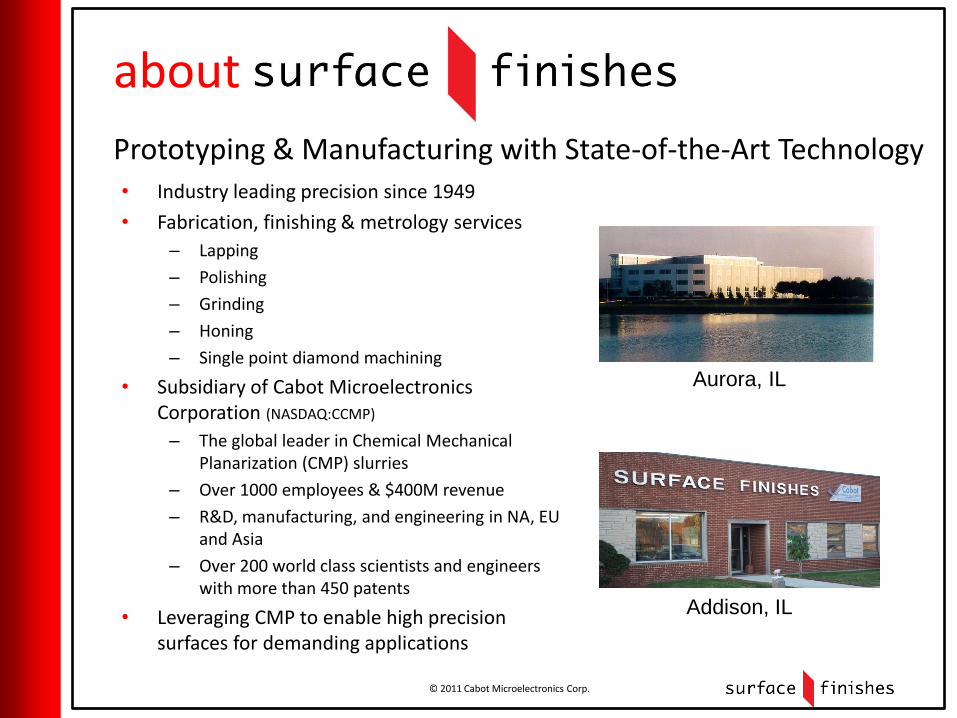
about Prototyping & Manufacturing with State-of-the-Art Technology • Industry leading precision since 1949
• Fabrication, finishing & metrology services
– Lapping
– Polishing
– Grinding
– Honing
– Single point diamond machining
• Subsidiary of Cabot Microelectronics Corporation (NASDAQ:CCMP)
– The global leader in Chemical Mechanical Planarization (CMP) slurries
– Over 1000 employees & $400M revenue
– R&D, manufacturing, and engineering in NA, EU and Asia
– Over 200 world class scientists and engineers with more than 450 patents
• Leveraging CMP to enable high precision surfaces for demanding applications
Addison, IL
Aurora, IL
© 2011 Cabot Microelectronics Corp.
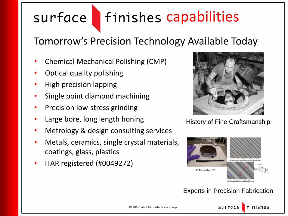
capabilities
Tomorrow’s Precision Technology Available Today
• Chemical Mechanical Polishing (CMP)
• Optical quality polishing
• High precision lapping
• Single point diamond machining
• Precision low-stress grinding
• Large bore, long length honing
• Metrology & design consulting services
• Metals, ceramics, single crystal materials, coatings, glass, plastics
• ITAR registered (#0049272)
History of Fine Craftsmanship
Experts in Precision Fabrication
© 2011 Cabot Microelectronics Corp.
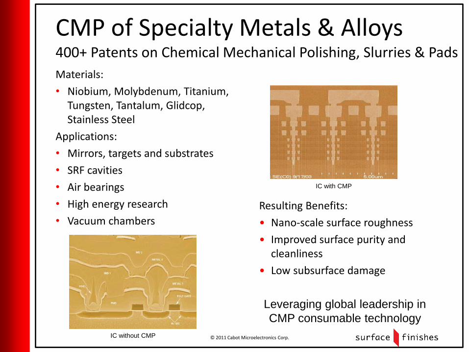
CMP of Specialty Metals & Alloys 400+ Patents on Chemical Mechanical Polishing, Slurries & Pads
Resulting Benefits:
• Nano-scale surface roughness
• Improved surface purity and cleanliness
• Low subsurface damage
Materials:
• Niobium, Molybdenum, Titanium, Tungsten, Tantalum, Glidcop, Stainless Steel
Applications:
• Mirrors, targets and substrates
• SRF cavities
• Air bearings
• High energy research
• Vacuum chambers
IC without CMP
IC with CMP
Leveraging global leadership in
CMP consumable technology
© 2011 Cabot Microelectronics Corp.
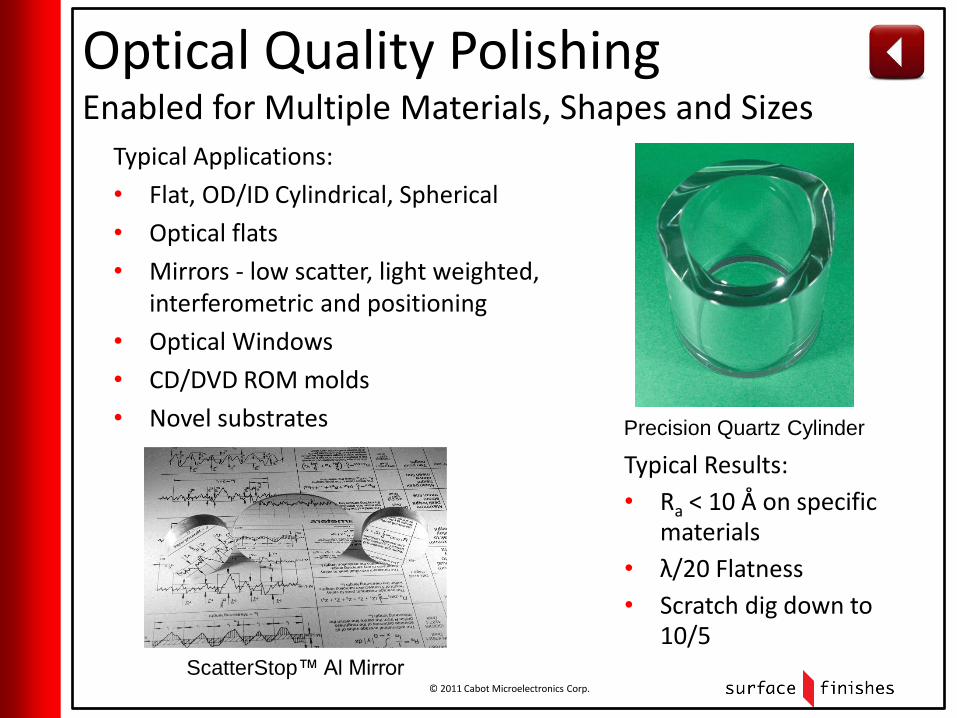
Optical Quality Polishing Enabled for Multiple Materials, Shapes and Sizes
Typical Applications:
• Flat, OD/ID Cylindrical, Spherical
• Optical flats
• Mirrors - low scatter, light weighted, interferometric and positioning
• Optical Windows
• CD/DVD ROM molds
• Novel substrates
Typical Results:
• Ra < 10 Å on specific materials
• λ/20 Flatness
• Scratch dig down to 10/5
Precision Quartz Cylinder
ScatterStop™ Al Mirror
© 2011 Cabot Microelectronics Corp.
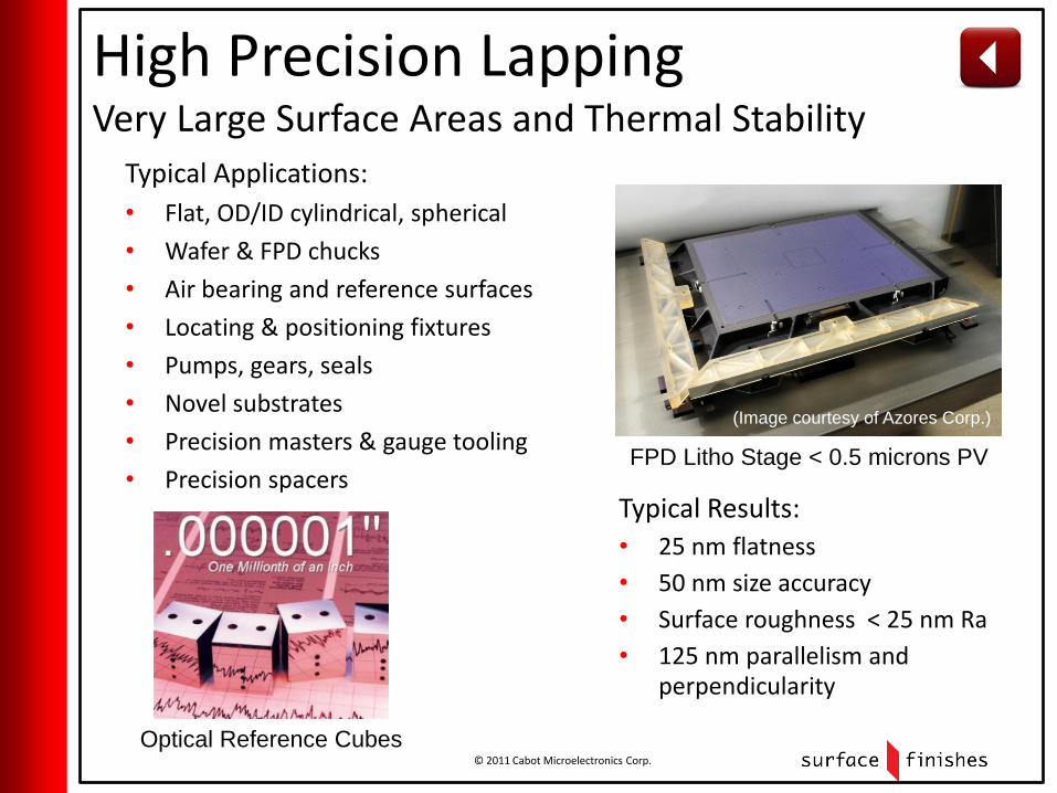
High Precision Lapping Very Large Surface Areas and Thermal Stability
Typical Applications:
• Flat, OD/ID cylindrical, spherical
• Wafer & FPD chucks
• Air bearing and reference surfaces
• Locating & positioning fixtures
• Pumps, gears, seals
• Novel substrates
• Precision masters & gauge tooling
• Precision spacers Typical Results:
• 25 nm flatness
• 50 nm size accuracy
• Surface roughness < 25 nm Ra
• 125 nm parallelism and perpendicularity
(Image courtesy of Azores Corp.)
Optical Reference Cubes
FPD Litho Stage < 0.5 microns PV
© 2011 Cabot Microelectronics Corp.
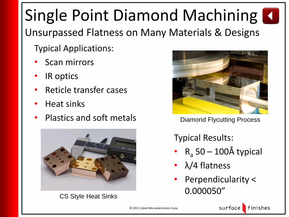
Single Point Diamond Machining Unsurpassed Flatness on Many Materials & Designs
Typical Applications:
• Scan mirrors
• IR optics
• Reticle transfer cases
• Heat sinks
• Plastics and soft metals
Typical Results:
• Ra 50 – 100Å typical
• λ/4 flatness
• Perpendicularity < 0.000050”
Diamond Flycutting Process
CS Style Heat Sinks
© 2011 Cabot Microelectronics Corp.
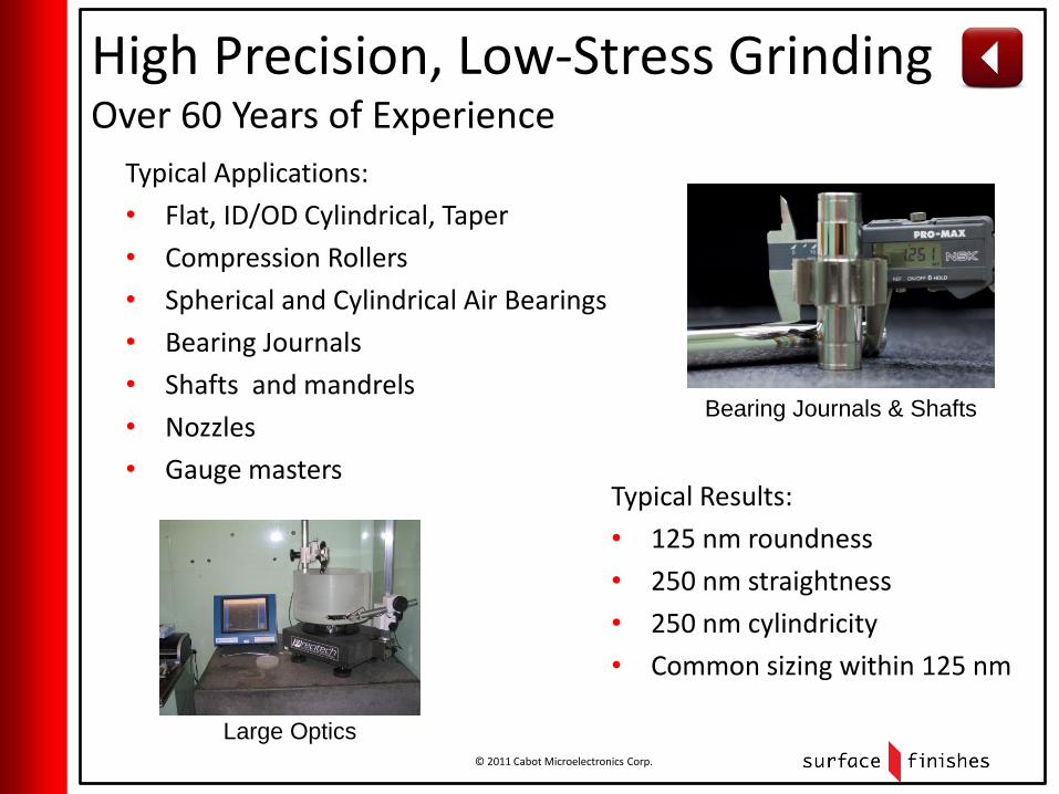
High Precision, Low-Stress Grinding Over 60 Years of Experience
Typical Applications:
• Flat, ID/OD Cylindrical, Taper
• Compression Rollers
• Spherical and Cylindrical Air Bearings
• Bearing Journals
• Shafts and mandrels
• Nozzles
• Gauge masters Typical Results:
• 125 nm roundness
• 250 nm straightness
• 250 nm cylindricity
• Common sizing within 125 nm
Bearing Journals & Shafts
Large Optics
© 2011 Cabot Microelectronics Corp.
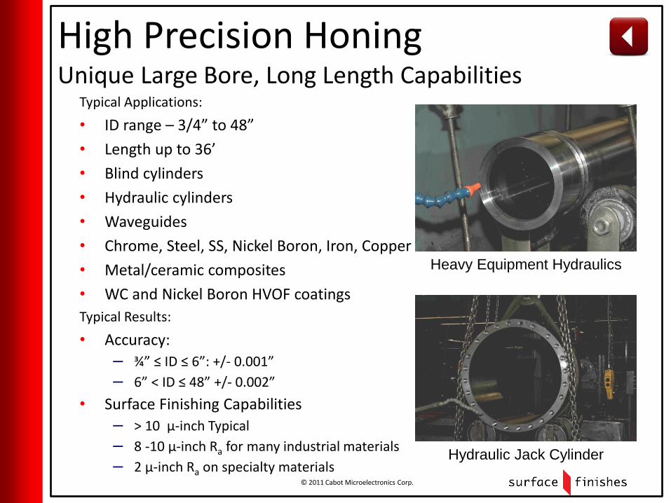
High Precision Honing Unique Large Bore, Long Length Capabilities
Typical Applications:
• ID range – 3/4” to 48”
• Length up to 36’
• Blind cylinders
• Hydraulic cylinders
• Waveguides
• Chrome, Steel, SS, Nickel Boron, Iron, Copper
• Metal/ceramic composites
• WC and Nickel Boron HVOF coatings
Typical Results:
• Accuracy:
– ¾” ≤ ID ≤ 6”: +/- 0.001”
– 6” < ID ≤ 48” +/- 0.002”
• Surface Finishing Capabilities
– > 10 µ-inch Typical
– 8 -10 µ-inch Ra for many industrial materials
– 2 µ-inch Ra on specialty materials
Heavy Equipment Hydraulics
Hydraulic Jack Cylinder
© 2011 Cabot Microelectronics Corp.
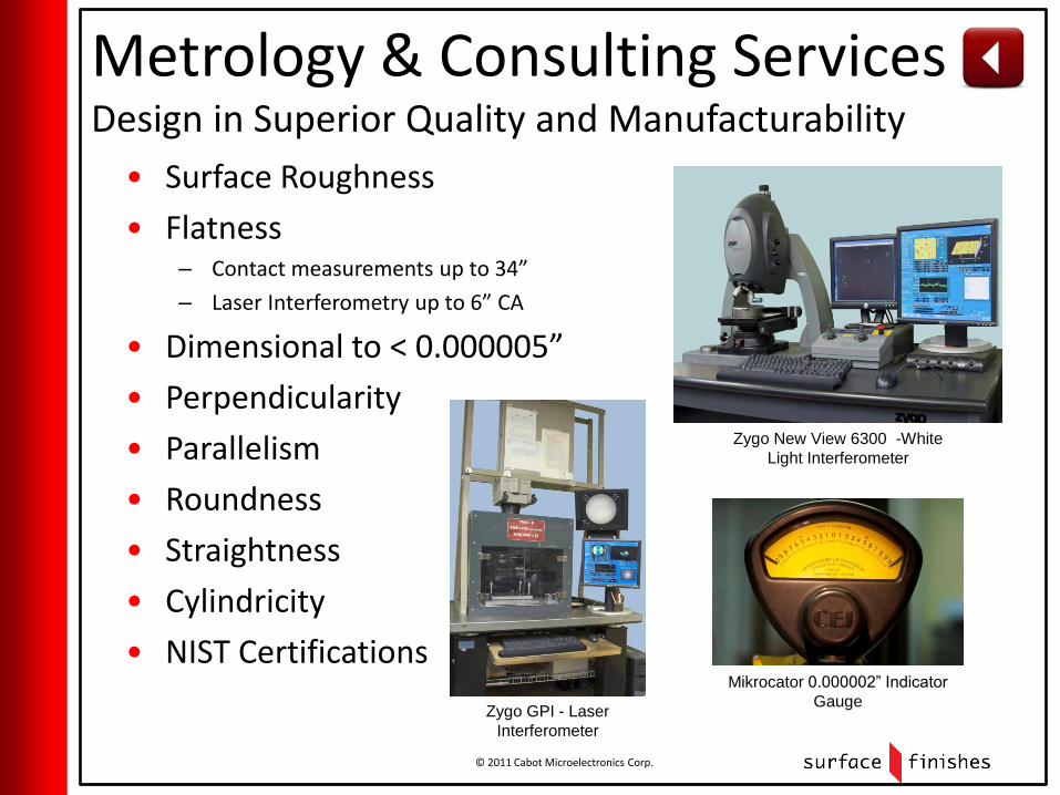
Metrology & Consulting Services Design in Superior Quality and Manufacturability
• Surface Roughness
• Flatness – Contact measurements up to 34”
– Laser Interferometry up to 6” CA
• Dimensional to < 0.000005”
• Perpendicularity
• Parallelism
• Roundness
• Straightness
• Cylindricity
• NIST Certifications
Zygo New View 6300 -White
Light Interferometer
Zygo GPI - Laser
Interferometer
Mikrocator 0.000002” Indicator
Gauge
© 2011 Cabot Microelectronics Corp.
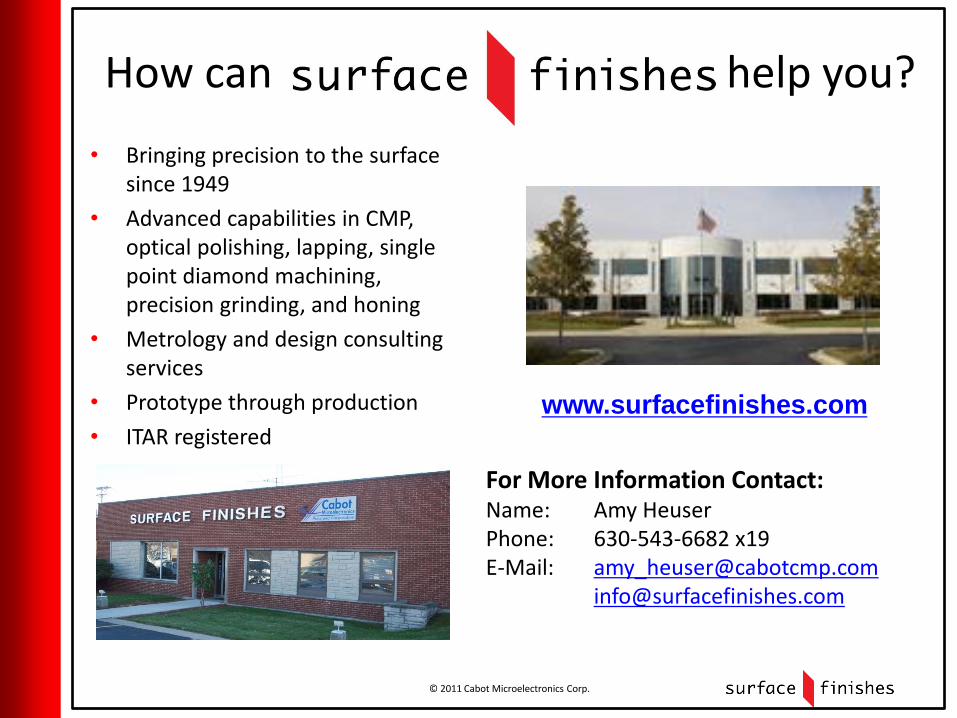
How can help you?
• Bringing precision to the surface since 1949
• Advanced capabilities in CMP, optical polishing, lapping, single point diamond machining, precision grinding, and honing
• Metrology and design consulting services
• Prototype through production
• ITAR registered
For More Information Contact: Name: Amy Heuser Phone: 630-543-6682 x19 E-Mail: [email protected] [email protected]
www.surfacefinishes.com
© 2011 Cabot Microelectronics Corp.
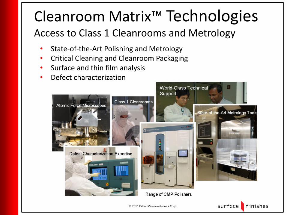
Cleanroom Matrix™ Technologies Access to Class 1 Cleanrooms and Metrology
• State-of-the-Art Polishing and Metrology • Critical Cleaning and Cleanroom Packaging • Surface and thin film analysis • Defect characterization
© 2011 Cabot Microelectronics Corp.
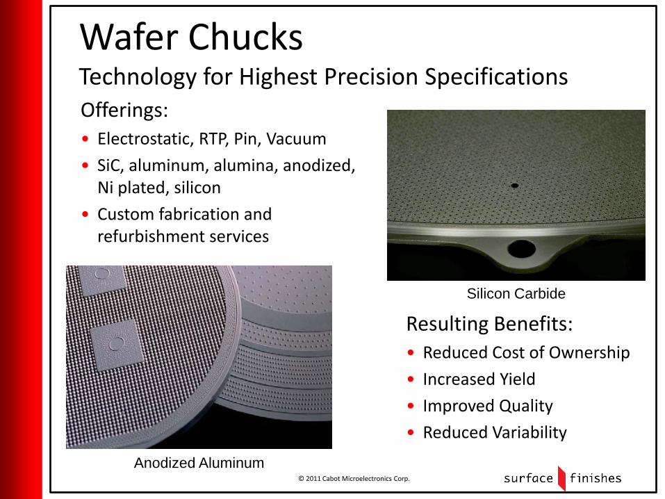
Wafer Chucks Technology for Highest Precision Specifications Offerings: • Electrostatic, RTP, Pin, Vacuum
• SiC, aluminum, alumina, anodized, Ni plated, silicon
• Custom fabrication and refurbishment services
Resulting Benefits: • Reduced Cost of Ownership
• Increased Yield
• Improved Quality
• Reduced Variability
Anodized Aluminum
Silicon Carbide
© 2011 Cabot Microelectronics Corp.
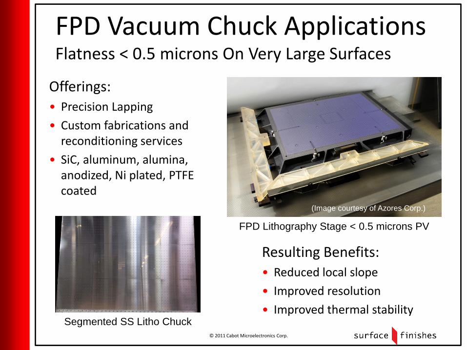
FPD Vacuum Chuck Applications Flatness < 0.5 microns On Very Large Surfaces
Offerings: • Precision Lapping
• Custom fabrications and reconditioning services
• SiC, aluminum, alumina, anodized, Ni plated, PTFE coated
(Image courtesy of Azores Corp.)
Resulting Benefits: • Reduced local slope
• Improved resolution
• Improved thermal stability Segmented SS Litho Chuck
(Image courtesy of Azores Corp.)
FPD Lithography Stage < 0.5 microns PV
© 2011 Cabot Microelectronics Corp.
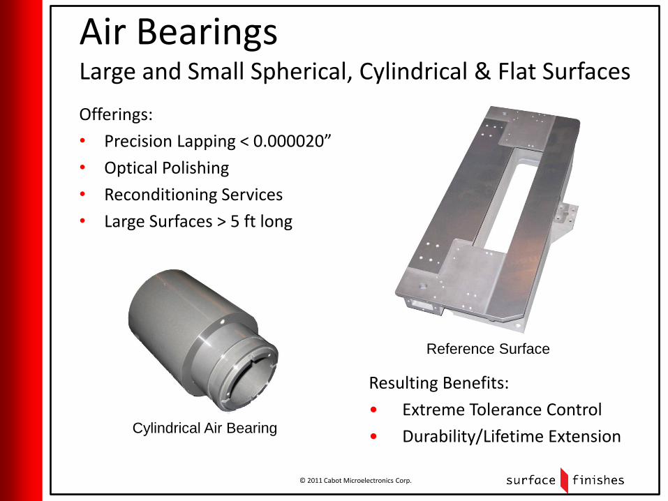
Air Bearings Large and Small Spherical, Cylindrical & Flat Surfaces
Offerings:
• Precision Lapping < 0.000020”
• Optical Polishing
• Reconditioning Services
• Large Surfaces > 5 ft long
Resulting Benefits:
• Extreme Tolerance Control
• Durability/Lifetime Extension
Reference Surface
Cylindrical Air Bearing
© 2011 Cabot Microelectronics Corp.
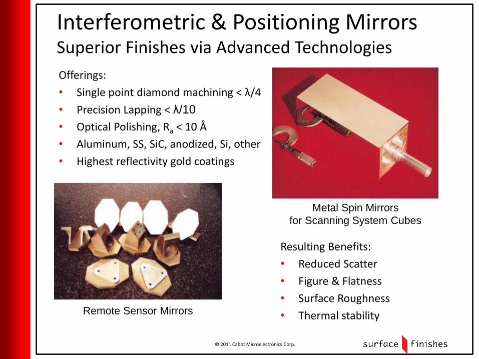
Interferometric & Positioning Mirrors Superior Finishes via Advanced Technologies
Remote Sensor Mirrors
Offerings:
• Single point diamond machining < λ/4
• Precision Lapping < λ/10
• Optical Polishing, Ra < 10 Å
• Aluminum, SS, SiC, anodized, Si, other
• Highest reflectivity gold coatings
Resulting Benefits:
• Reduced Scatter
• Figure & Flatness
• Surface Roughness
• Thermal stability
Metal Spin Mirrors
for Scanning System Cubes
© 2011 Cabot Microelectronics Corp.
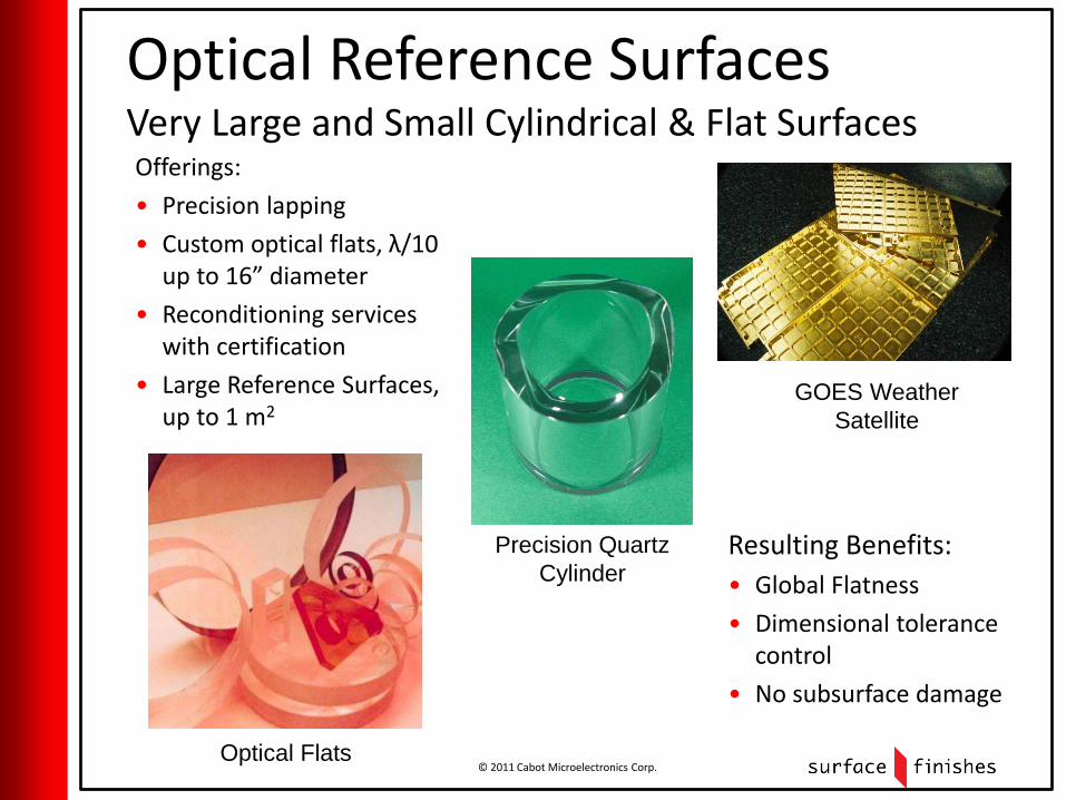
Optical Reference Surfaces Very Large and Small Cylindrical & Flat Surfaces Offerings:
• Precision lapping
• Custom optical flats, λ/10 up to 16” diameter
• Reconditioning services with certification
• Large Reference Surfaces, up to 1 m2
Resulting Benefits:
• Global Flatness
• Dimensional tolerance control
• No subsurface damage
Optical Flats
GOES Weather
Satellite
Precision Quartz
Cylinder
© 2011 Cabot Microelectronics Corp.
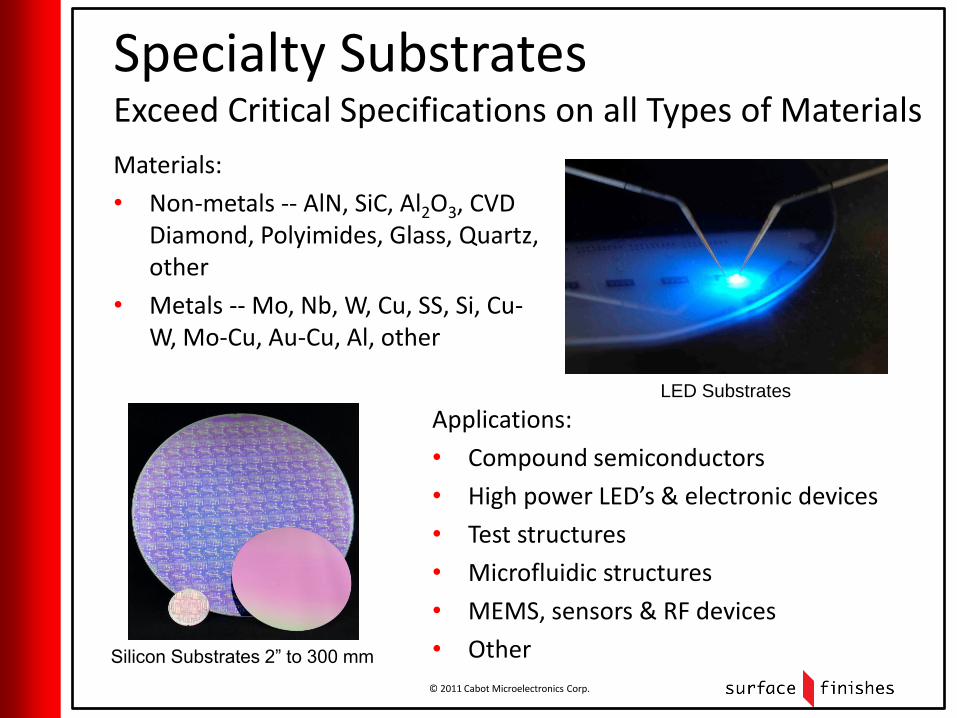
Specialty Substrates Exceed Critical Specifications on all Types of Materials
Materials:
• Non-metals -- AlN, SiC, Al2O3, CVD Diamond, Polyimides, Glass, Quartz, other
• Metals -- Mo, Nb, W, Cu, SS, Si, Cu-W, Mo-Cu, Au-Cu, Al, other
Applications:
• Compound semiconductors
• High power LED’s & electronic devices
• Test structures
• Microfluidic structures
• MEMS, sensors & RF devices
• Other
LED Substrates
Silicon Substrates 2” to 300 mm
© 2011 Cabot Microelectronics Corp.
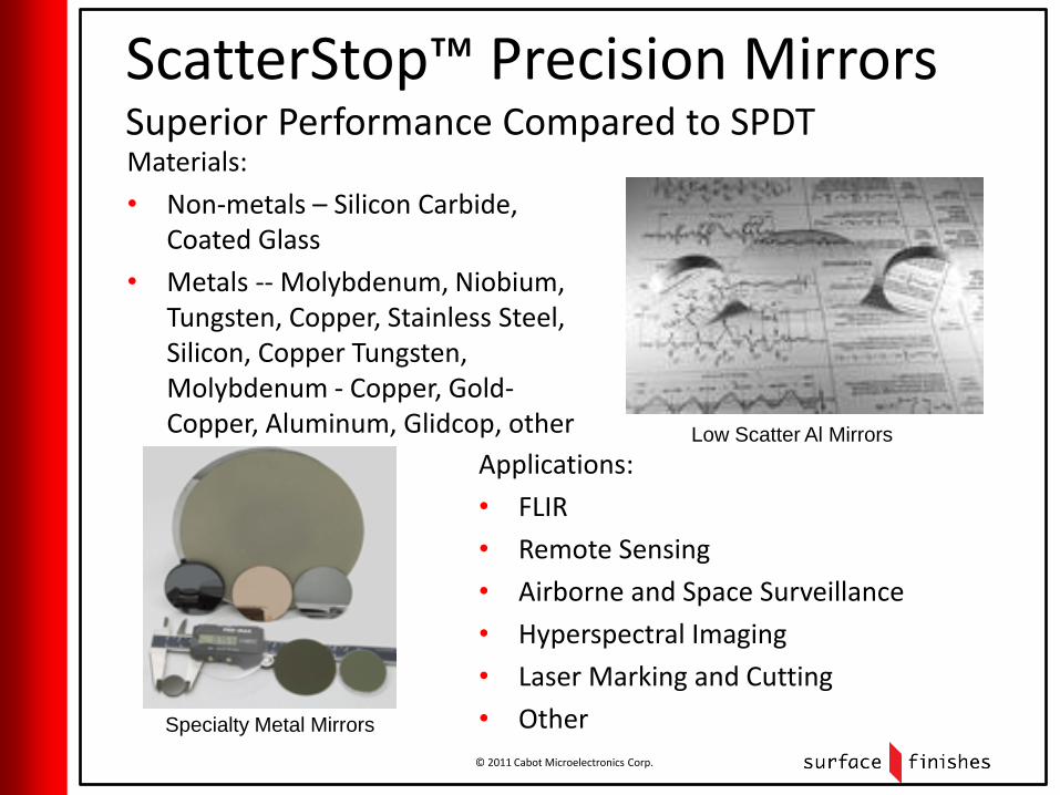
ScatterStop™ Precision Mirrors Superior Performance Compared to SPDT Materials:
• Non-metals – Silicon Carbide, Coated Glass
• Metals -- Molybdenum, Niobium, Tungsten, Copper, Stainless Steel, Silicon, Copper Tungsten, Molybdenum - Copper, Gold-Copper, Aluminum, Glidcop, other
Applications:
• FLIR
• Remote Sensing
• Airborne and Space Surveillance
• Hyperspectral Imaging
• Laser Marking and Cutting
• Other
Low Scatter Al Mirrors
Specialty Metal Mirrors
© 2011 Cabot Microelectronics Corp.
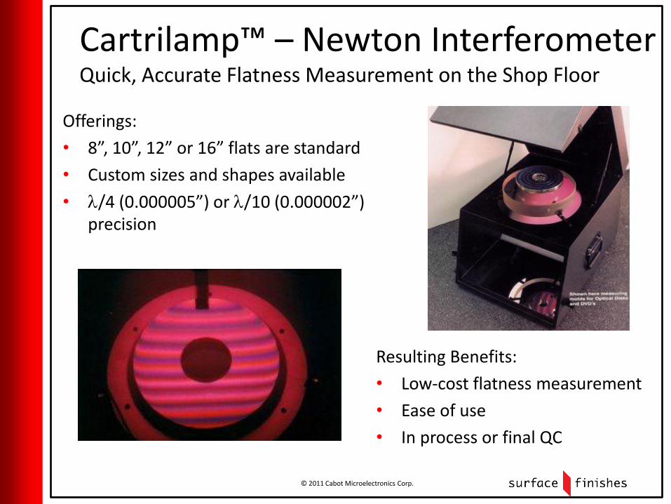
Cartrilamp™ – Newton Interferometer Quick, Accurate Flatness Measurement on the Shop Floor
Offerings:
• 8”, 10”, 12” or 16” flats are standard
• Custom sizes and shapes available
• l/4 (0.000005”) or l/10 (0.000002”) precision
Resulting Benefits:
• Low-cost flatness measurement
• Ease of use
• In process or final QC
© 2011 Cabot Microelectronics Corp.
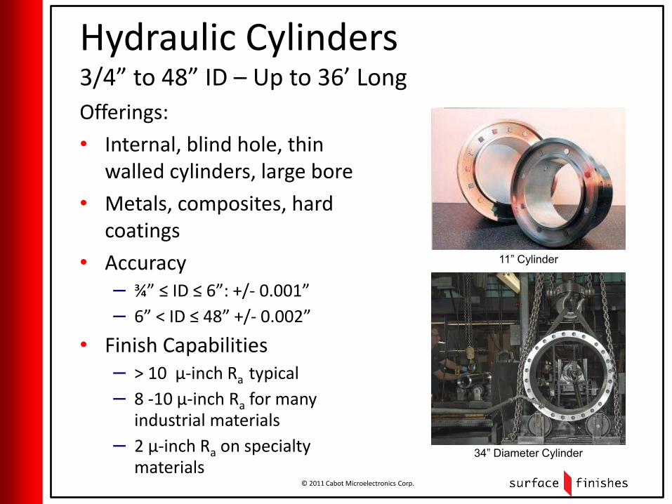
Hydraulic Cylinders 3/4” to 48” ID – Up to 36’ Long
Offerings:
• Internal, blind hole, thin walled cylinders, large bore
• Metals, composites, hard coatings
• Accuracy – ¾” ≤ ID ≤ 6”: +/- 0.001”
– 6” < ID ≤ 48” +/- 0.002”
• Finish Capabilities – > 10 µ-inch Ra typical
– 8 -10 µ-inch Ra for many industrial materials
– 2 µ-inch Ra on specialty materials
11” Cylinder
34” Diameter Cylinder
© 2011 Cabot Microelectronics Corp.
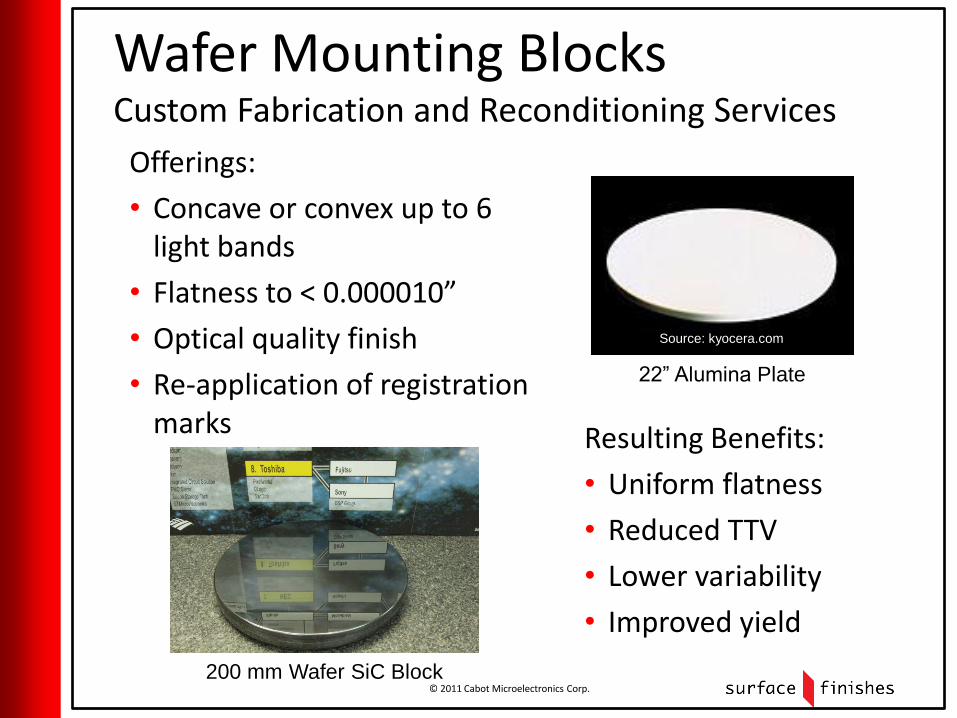
Wafer Mounting Blocks Custom Fabrication and Reconditioning Services
Resulting Benefits:
• Uniform flatness
• Reduced TTV
• Lower variability
• Improved yield
Offerings:
• Concave or convex up to 6 light bands
• Flatness to < 0.000010”
• Optical quality finish
• Re-application of registration marks
22” Alumina Plate
200 mm Wafer SiC Block
Source: kyocera.com
Source: kyocera.com
© 2011 Cabot Microelectronics Corp.
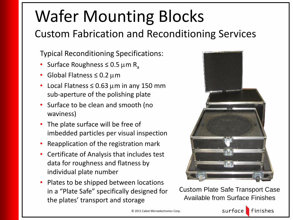
Wafer Mounting Blocks Custom Fabrication and Reconditioning Services
Typical Reconditioning Specifications:
• Surface Roughness ≤ 0.5 mm Ra
• Global Flatness ≤ 0.2 mm
• Local Flatness ≤ 0.63 mm in any 150 mm sub-aperture of the polishing plate
• Surface to be clean and smooth (no waviness)
• The plate surface will be free of imbedded particles per visual inspection
• Reapplication of the registration mark
• Certificate of Analysis that includes test data for roughness and flatness by individual plate number
• Plates to be shipped between locations in a “Plate Safe” specifically designed for the plates’ transport and storage
Custom Plate Safe Transport Case
Available from Surface Finishes
© 2011 Cabot Microelectronics Corp.
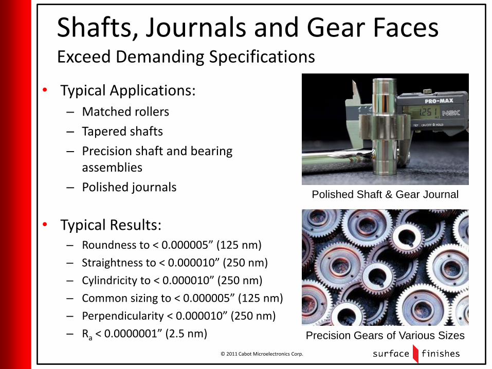
Shafts, Journals and Gear Faces Exceed Demanding Specifications
• Typical Applications: – Matched rollers
– Tapered shafts
– Precision shaft and bearing assemblies
– Polished journals
• Typical Results: – Roundness to < 0.000005” (125 nm)
– Straightness to < 0.000010” (250 nm)
– Cylindricity to < 0.000010” (250 nm)
– Common sizing to < 0.000005” (125 nm)
– Perpendicularity < 0.000010” (250 nm)
– Ra < 0.0000001” (2.5 nm)
Polished Shaft & Gear Journal
Precision Gears of Various Sizes
© 2011 Cabot Microelectronics Corp.
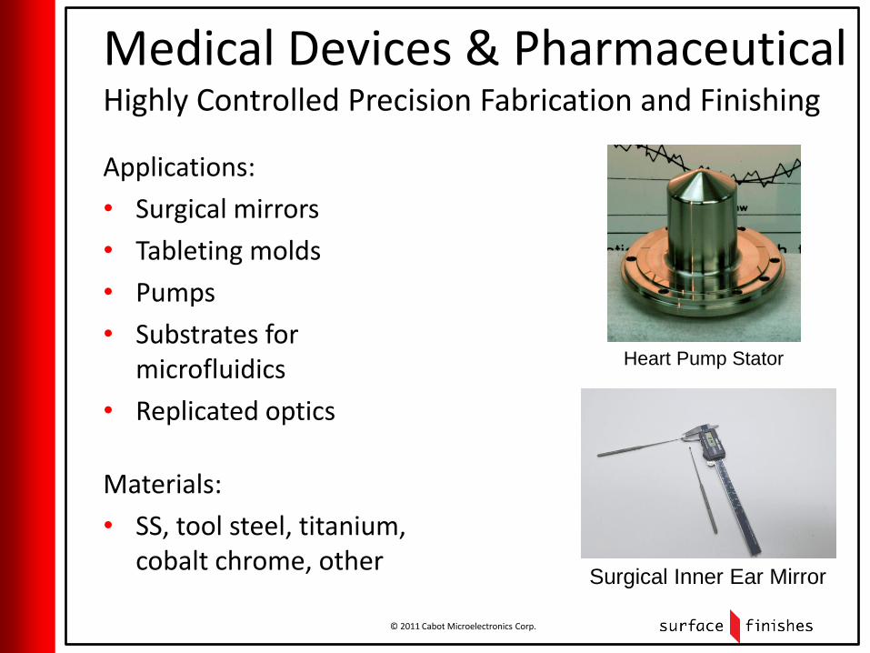
Medical Devices & Pharmaceutical Highly Controlled Precision Fabrication and Finishing
Applications:
• Surgical mirrors
• Tableting molds
• Pumps
• Substrates for microfluidics
• Replicated optics
Materials:
• SS, tool steel, titanium, cobalt chrome, other
Heart Pump Stator
Surgical Inner Ear Mirror
© 2011 Cabot Microelectronics Corp.
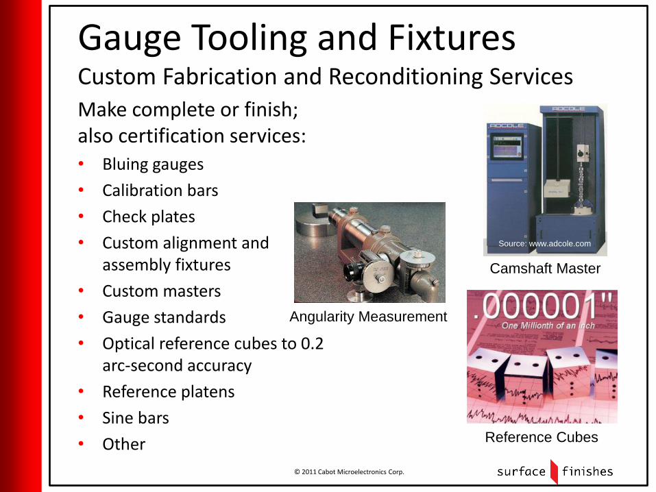
Gauge Tooling and Fixtures Custom Fabrication and Reconditioning Services
Make complete or finish; also certification services: • Bluing gauges
• Calibration bars
• Check plates
• Custom alignment and assembly fixtures
• Custom masters
• Gauge standards
• Optical reference cubes to 0.2 arc-second accuracy
• Reference platens
• Sine bars
• Other
Source: www.adcole.com
Camshaft Master
Angularity Measurement
Reference Cubes
© 2011 Cabot Microelectronics Corp.
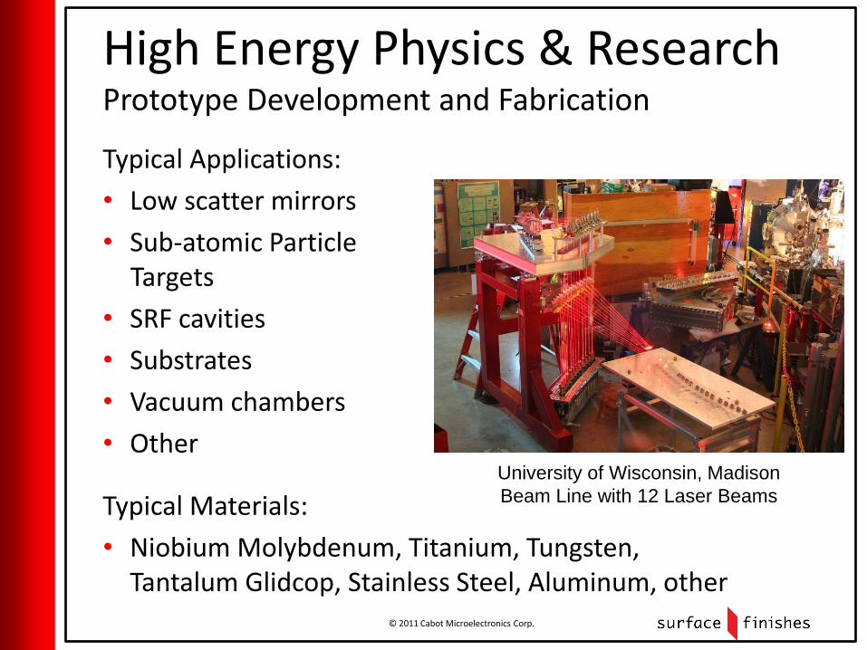
High Energy Physics & Research Prototype Development and Fabrication
Typical Applications:
• Low scatter mirrors
• Sub-atomic Particle Targets
• SRF cavities
• Substrates
• Vacuum chambers
• Other
Typical Materials:
• Niobium Molybdenum, Titanium, Tungsten, Tantalum Glidcop, Stainless Steel, Aluminum, other
University of Wisconsin, Madison
Beam Line with 12 Laser Beams
© 2011 Cabot Microelectronics Corp.
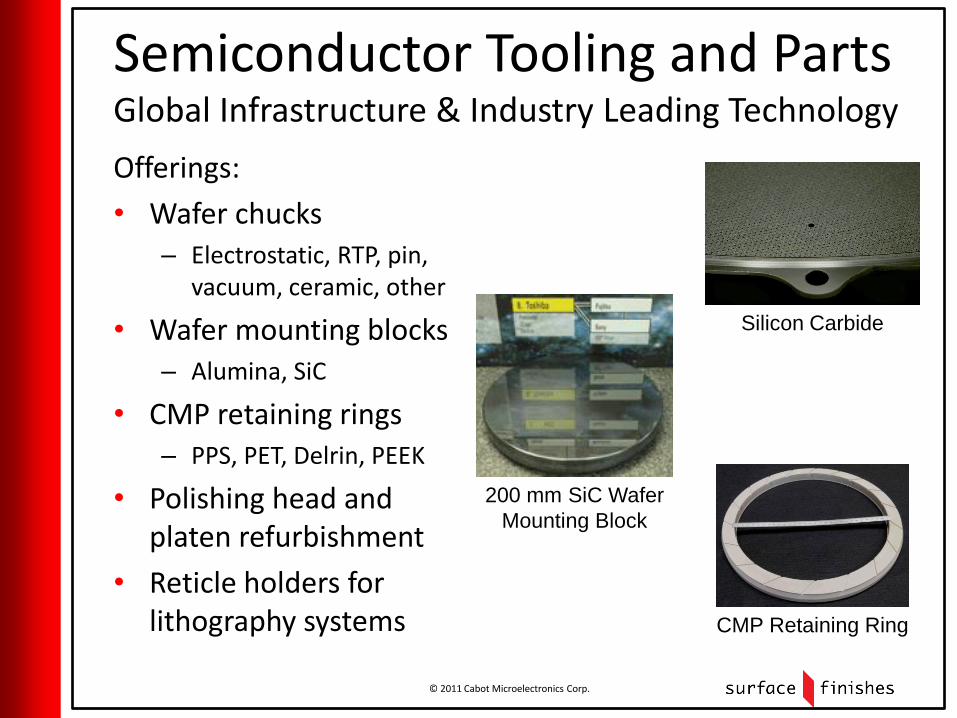
Semiconductor Tooling and Parts Global Infrastructure & Industry Leading Technology
Offerings:
• Wafer chucks – Electrostatic, RTP, pin,
vacuum, ceramic, other
• Wafer mounting blocks – Alumina, SiC
• CMP retaining rings – PPS, PET, Delrin, PEEK
• Polishing head and platen refurbishment
• Reticle holders for lithography systems
Silicon Carbide
CMP Retaining Ring
200 mm SiC Wafer
Mounting Block
© 2011 Cabot Microelectronics Corp.
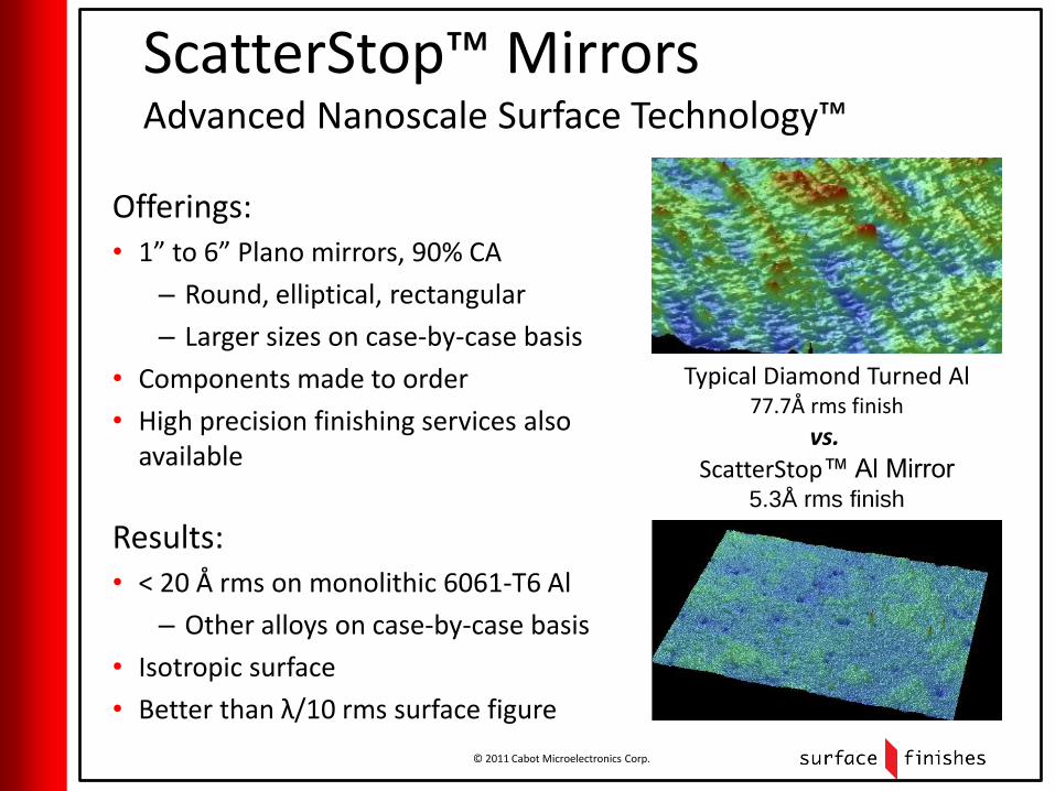
ScatterStop™ Mirrors Advanced Nanoscale Surface Technology™
Offerings: • 1” to 6” Plano mirrors, 90% CA
– Round, elliptical, rectangular
– Larger sizes on case-by-case basis
• Components made to order
• High precision finishing services also available
Results: • < 20 Å rms on monolithic 6061-T6 Al
– Other alloys on case-by-case basis
• Isotropic surface
• Better than λ/10 rms surface figure
ESF ScatterStop™ Al Mirror
Typical Diamond Turned Al 77.7Å rms finish
ScatterStop™ Al Mirror 5.3Å rms finish
vs.
© 2011 Cabot Microelectronics Corp.
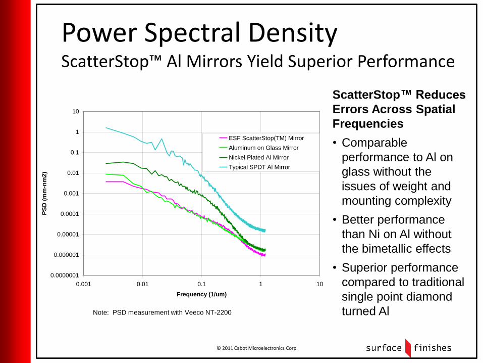
Power Spectral Density ScatterStop™ Al Mirrors Yield Superior Performance
ScatterStop™ Reduces
Errors Across Spatial
Frequencies
• Comparable
performance to Al on
glass without the
issues of weight and
mounting complexity
• Better performance
than Ni on Al without
the bimetallic effects
• Superior performance
compared to traditional
single point diamond
turned Al
0.0000001
0.000001
0.00001
0.0001
0.001
0.01
0.1
1
10
0.001 0.01 0.1 1 10
Frequency (1/um)
PS
D (
mm
-nm
2)
ESF ScatterStop(TM) Mirror
Aluminum on Glass Mirror
Nickel Plated Al Mirror
Typical SPDT Al Mirror
Note: PSD measurement with Veeco NT-2200
© 2011 Cabot Microelectronics Corp.
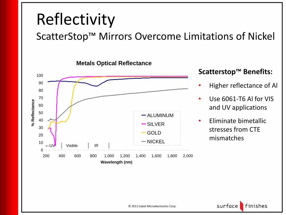
Reflectivity ScatterStop™ Mirrors Overcome Limitations of Nickel
Scatterstop™ Benefits:
• Higher reflectance of Al
• Use 6061-T6 Al for VIS and UV applications
• Eliminate bimetallic stresses from CTE mismatches
Metals Optical Reflectance
0
10
20
30
40
50
60
70
80
90
100
200 400 600 800 1,000 1,200 1,400 1,600 1,800 2,000
Wavelength (nm)
% R
efl
ecta
nce
ALUMINUM
SILVER
GOLD
NICKELIR Visible ←UV
© 2011 Cabot Microelectronics Corp.
Many ScatterStop™ Applications Superior Performance compared to SPDT
Typical Applications:
• FLIR
• Targeting and fire control
• Image stabilization
• Remote sensing
• Printing and scanning
• Microscopy
• Airborne and space surveillance
• Semiconductor inspection
• Hyperspectral Imaging
• Laser Beam Delivery
• Laser marking and cutting
• Machine Vision/Sorting
• Medical Imaging
• Spectrometers
• Free space laser communication
© 2011 Cabot Microelectronics Corp.
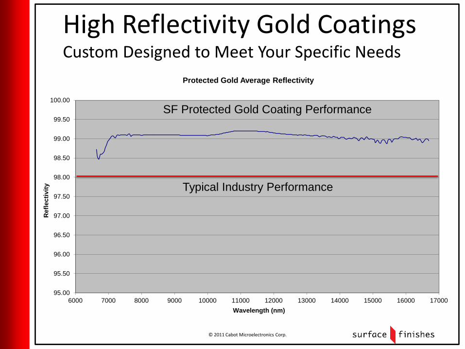
High Reflectivity Gold Coatings Custom Designed to Meet Your Specific Needs
95.00
95.50
96.00
96.50
97.00
97.50
98.00
98.50
99.00
99.50
100.00
6000 7000 8000 9000 10000 11000 12000 13000 14000 15000 16000 17000
Refl
ecti
vit
y
Wavelength (nm)
Protected Gold Average Reflectivity
Typical Industry Performance
SF Protected Gold Coating Performance
© 2011 Cabot Microelectronics Corp.
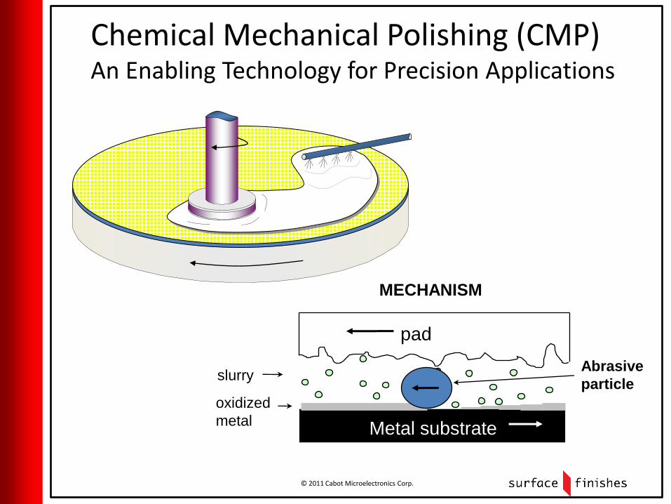
Chemical Mechanical Polishing (CMP) An Enabling Technology for Precision Applications
Abrasive
particle
pad
slurry
oxidized
metal Metal substrate
MECHANISM
© 2011 Cabot Microelectronics Corp.
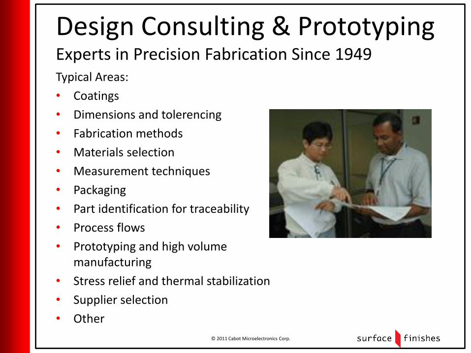
Design Consulting & Prototyping Experts in Precision Fabrication Since 1949 Typical Areas:
• Coatings
• Dimensions and tolerencing
• Fabrication methods
• Materials selection
• Measurement techniques
• Packaging
• Part identification for traceability
• Process flows
• Prototyping and high volume manufacturing
• Stress relief and thermal stabilization
• Supplier selection
• Other
© 2011 Cabot Microelectronics Corp.
Refurbishment and Certification Significantly Reduce Costs by Extending Service Life Typical Applications:
• Calendaring rolls
• CD and DVD molds
• Check & reference plates
• Gauge tooling & masters
• Hydraulic cylinders
• Optical reference surfaces
• Pin & vacuum chucks
• Seals
• Slitter knives
• Tableting molds
• Valve components
• Wafer mounting blocks
• Wobblers
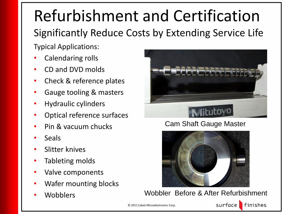
Cam Shaft Gauge Master
Wobbler Before & After Refurbishment
© 2011 Cabot Microelectronics Corp.
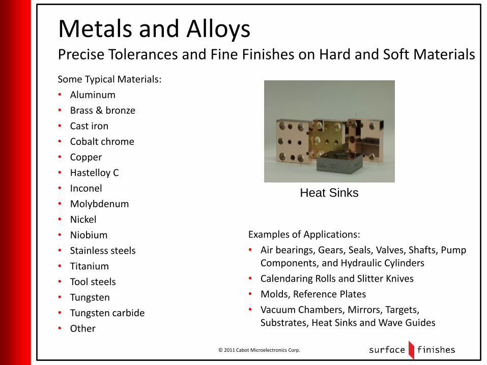
Metals and Alloys Precise Tolerances and Fine Finishes on Hard and Soft Materials
Examples of Applications:
• Air bearings, Gears, Seals, Valves, Shafts, Pump Components, and Hydraulic Cylinders
• Calendaring Rolls and Slitter Knives
• Molds, Reference Plates
• Vacuum Chambers, Mirrors, Targets, Substrates, Heat Sinks and Wave Guides
Some Typical Materials:
• Aluminum
• Brass & bronze
• Cast iron
• Cobalt chrome
• Copper
• Hastelloy C
• Inconel
• Molybdenum
• Nickel
• Niobium
• Stainless steels
• Titanium
• Tool steels
• Tungsten
• Tungsten carbide
• Other
Heat Sinks
© 2011 Cabot Microelectronics Corp.
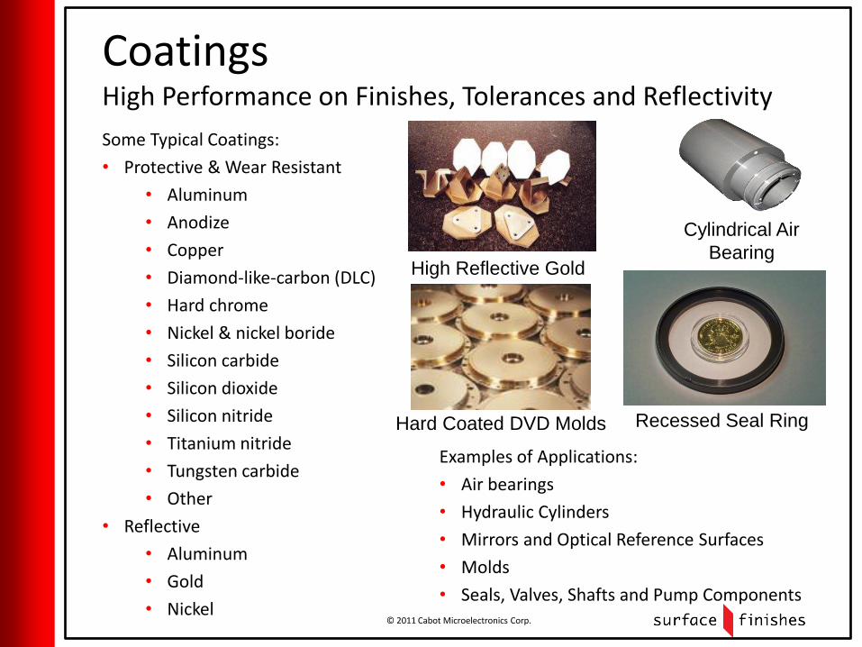
High Reflective Gold
Coatings High Performance on Finishes, Tolerances and Reflectivity
Examples of Applications:
• Air bearings
• Hydraulic Cylinders
• Mirrors and Optical Reference Surfaces
• Molds
• Seals, Valves, Shafts and Pump Components
Some Typical Coatings:
• Protective & Wear Resistant
• Aluminum
• Anodize
• Copper
• Diamond-like-carbon (DLC)
• Hard chrome
• Nickel & nickel boride
• Silicon carbide
• Silicon dioxide
• Silicon nitride
• Titanium nitride
• Tungsten carbide
• Other
• Reflective
• Aluminum
• Gold
• Nickel
Cylindrical Air
Bearing
Recessed Seal Ring Hard Coated DVD Molds
© 2011 Cabot Microelectronics Corp.
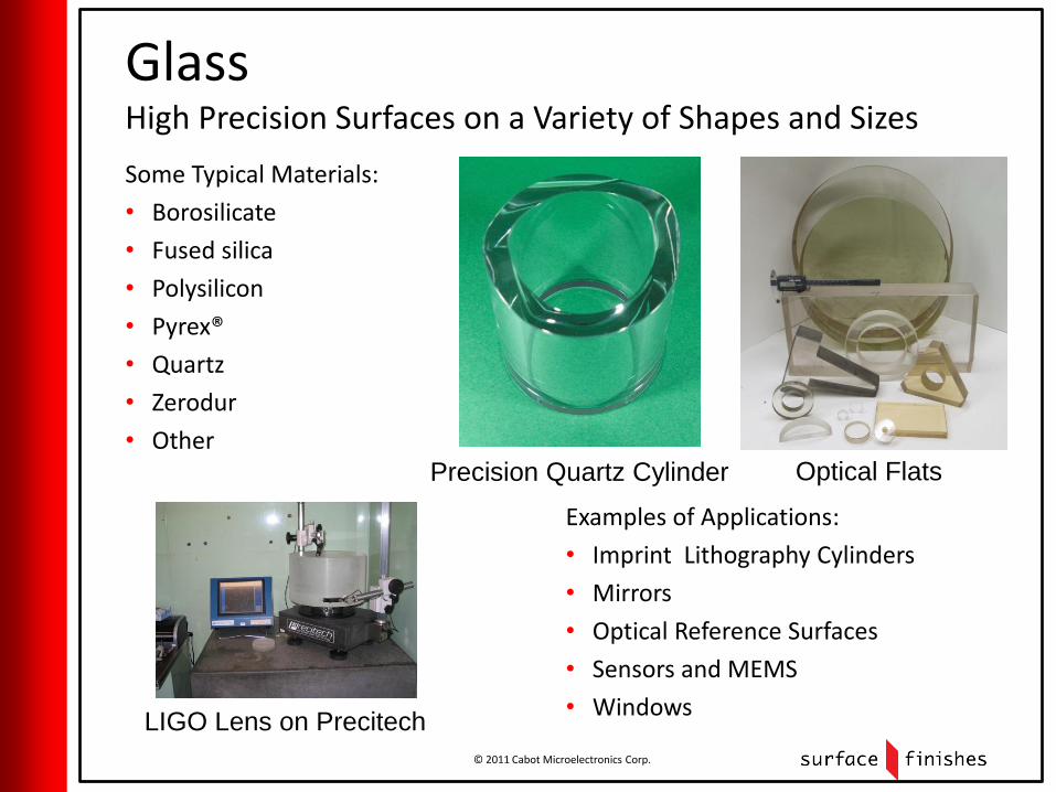
Glass High Precision Surfaces on a Variety of Shapes and Sizes
Examples of Applications:
• Imprint Lithography Cylinders
• Mirrors
• Optical Reference Surfaces
• Sensors and MEMS
• Windows
Some Typical Materials:
• Borosilicate
• Fused silica
• Polysilicon
• Pyrex®
• Quartz
• Zerodur
• Other
Optical Flats
LIGO Lens on Precitech
Precision Quartz Cylinder
© 2011 Cabot Microelectronics Corp.
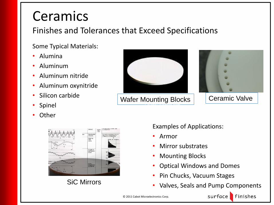
Ceramics Finishes and Tolerances that Exceed Specifications
Examples of Applications:
• Armor
• Mirror substrates
• Mounting Blocks
• Optical Windows and Domes
• Pin Chucks, Vacuum Stages
• Valves, Seals and Pump Components
Some Typical Materials:
• Alumina
• Aluminum
• Aluminum nitride
• Aluminum oxynitride
• Silicon carbide
• Spinel
• Other
SiC Mirrors
Wafer Mounting Blocks Ceramic Valve Source: kyocera.com
© 2011 Cabot Microelectronics Corp.
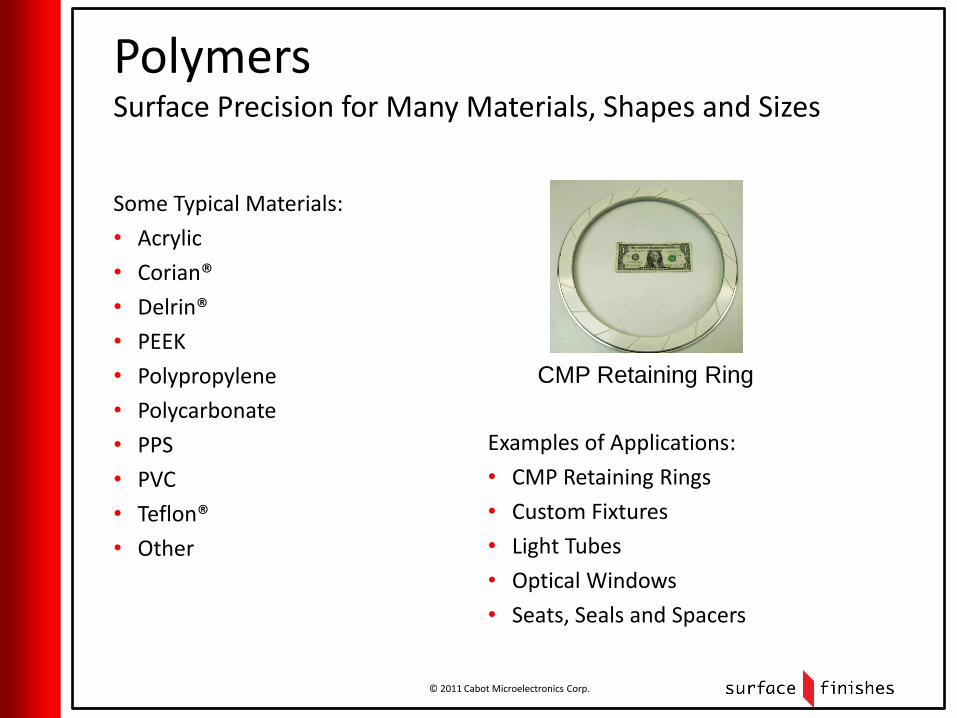
Polymers Surface Precision for Many Materials, Shapes and Sizes
Examples of Applications:
• CMP Retaining Rings
• Custom Fixtures
• Light Tubes
• Optical Windows
• Seats, Seals and Spacers
Some Typical Materials:
• Acrylic
• Corian®
• Delrin®
• PEEK
• Polypropylene
• Polycarbonate
• PPS
• PVC
• Teflon®
• Other
CMP Retaining Ring
© 2011 Cabot Microelectronics Corp.
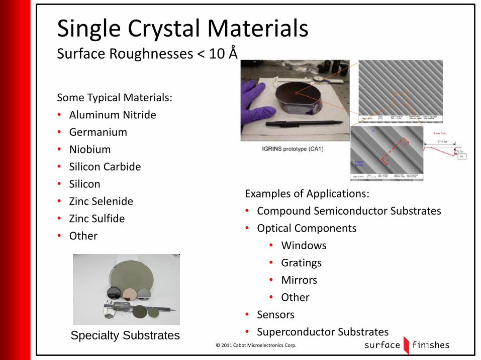
Single Crystal Materials Surface Roughnesses < 10 Å
Examples of Applications:
• Compound Semiconductor Substrates
• Optical Components
• Windows
• Gratings
• Mirrors
• Other
• Sensors
• Superconductor Substrates
Some Typical Materials:
• Aluminum Nitride
• Germanium
• Niobium
• Silicon Carbide
• Silicon
• Zinc Selenide
• Zinc Sulfide
• Other
Specialty Substrates