Optical spectroscopy as a probe of charge and energy transfer in two-dimensional materials Stéphane BERCIAUD IPCMS, Université de Strasbourg and CNRS [email protected]New Frontiers in 2D materials Winterschool/Workshop Villard de Lans, January 16, 2017
Transcript
Optical spectroscopy as a probe of charge and energy transfer
in two-dimensional materials
Stéphane BERCIAUD IPCMS, Université de Strasbourg and CNRS
Devices: Nanofabrication Custom devices Electrical control
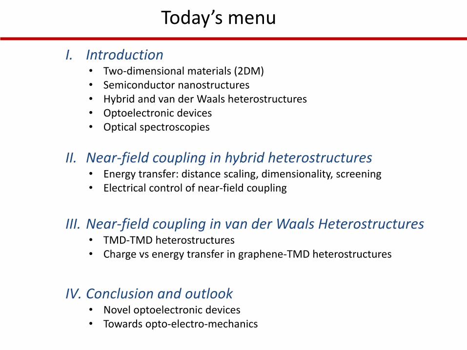
Today’s menu
I. Introduction • Two-dimensional materials (2DM) • Semiconductor nanostructures • Hybrid and van der Waals heterostructures • Optoelectronic devices • Optical spectroscopies
II. Near-field coupling in hybrid heterostructures • Energy transfer: distance scaling, dimensionality, screening • Electrical control of near-field coupling
III. Near-field coupling in van der Waals Heterostructures • TMD-TMD heterostructures • Charge vs energy transfer in graphene-TMD heterostructures
IV. Conclusion and outlook • Novel optoelectronic devices • Towards opto-electro-mechanics
Introducing 2D materials
Ajayan, Kim, Banerjee - Physics Today (2016)
Graphene: a unique, tunable 2D electron gas
FvkE
Momentum En
ergy
X Eex
VG VSD
Source Drain
Electric field effect
Si
SiO2
+ + + + + + + + + + +
- - - - - - - - - - - - - -
- - - - - - - - - - - - - -
E
1st observation: Novoselov et al., Science (2004) Data: G. Froehlicher and SB, PRB 91, 205413 2015 See also J. Yan et al. PRL 2007, Pisana et al. Nat Mater 2007
-5 0 5
2
3
So
urc
e-D
rain
cu
rre
nt I S
D (
µA
)
Gate Bias VG
(V)
EF <0
p doping
EF=0
EF >0
n doping
quantum electron transport (QHE) electron-phonon coupling electromechanics optoelectronics
Graphene: a unique, tunable 2D electron gas
FvkE
Momentum
Ener
gy
X Eex
VG VSD
Source Drain
Electric field effect
Si
SiO2
+ + + + + + + + + + +
- - - - - - - - - - - - - -
- - - - - - - - - - - - - -
E
1st observation: Novoselov et al., Science (2004)
quantum electron transport (QHE) electron-phonon coupling electromechanics optoelectronics
Z.Q. Li at al. Nature Physics (2008) F. Wang et al. Science (2008)
Absorption edge at E~2EF
• MX2 with M = Mo, W, Re,… X = S, Se, Te • Well documented in the bulk Wilson and Yoffe Adv. Phys. 1969
• All optical valley polarization Mak et al. + Zeng et al., Nat. Nano 2012
• Valley-Hall effect
K. F. Mak, PRL 105, 136805 (2010)
• Photodetection, electroluminescence, photovoltaics • Type II van der Waals heterostructures (Seattle, ICFO, Columbia, Berkeley, Manchester, MIT, Vienna, EPFL, U. Kansas,…)
Photonics
Optoelectronics
Valleytronics
• Indirect (bulk) to direct (1L) bandgap
• Tightly bound excions (trions, biexcitons)
• Single photon emitters* • Towards large PL quantum yields
Nat. Nano 2014 (TU Vienna, MIT, Seattle)
Mak et al. Science 2014
Columia, Berkeley, Case Western, Hong Kong, INSA Toulouse, Vanderbilt, LNCMI, Geneva… *Nat Nano 2015 (ETH, Rochester, LNCMI, Hefei/Seattle) Amani et al. Science 2015
Harnessing near-field interactions in new optoelectronic devices
Hybrid systems and heterostructures
Y. Liu et al., Nature Review Materials doi: 10.1038/natrevmats.2016.42
FRET in hybrid optoelectronic devices
Energy Transfer Pumping Achermann et al. Nature (2004) (Los Alamos)
+ Energy/exciton funnelling Substrate sensitization Color conversion Long Range (>> 1 nm) How to separate the transferred excitons?
B. Guzelturk & HV Demir Advanced Functional Materials 10.1002/adfm.201603311
Charge Transfer in hybrid photodetectors
Quartz
Ion gel VG
Gate
Drain VSD Source
Elaser
+ + +
+ +
+
+
+
- -
-
- - - -
-
Core “only” CQDs with short ligands
Graphene
High gain Photodetectors
+-
ElaserPhotoinduced
Charge Transfer
+ Photodetection Short range (< 1 nm) Selectivity/Sensitivity Processability
Short range… Highly sensitive to: Surface states Adsorbates Interfaces/ligands
Konstantatos et al. Nat. Nano (2012) (ICFO)
Charge Transfer in hybrid photodetectors
Quartz
Ion gel VG
Gate
Drain VSD Source
Elaser
+ + +
+ +
+
+
+
- -
-
- - - -
-
Core “only” CQDs with short ligands
Graphene
High gain Photodetectors
+-
ElaserPhotoinduced
Charge Transfer
+ Photodetection Short range (< 1 nm) Selectivity/Sensitivity Processability
Short range… Highly sensitive to: Surface states Adsorbates Interfaces/ligands
Kufer et al. Advanced Mat. (2015)
van der Waals Heterostructures
Haigh, Gorbachev et al., Nature Materials 2012 Manchester Group
Castellanos-Gomez et al. 2D Materials 1 011002 (2014)
No dangling bounds No lattice mismatch issues Rotational degree of freedom • 2010 : Graphene on hBN • 2017 : wet or dry transfer, pick up and lift,… • Numerous possibilities!
C-H Lee et al. Nat. Nano (2014) (Columbia)
Atomically thin p-n junctions
24
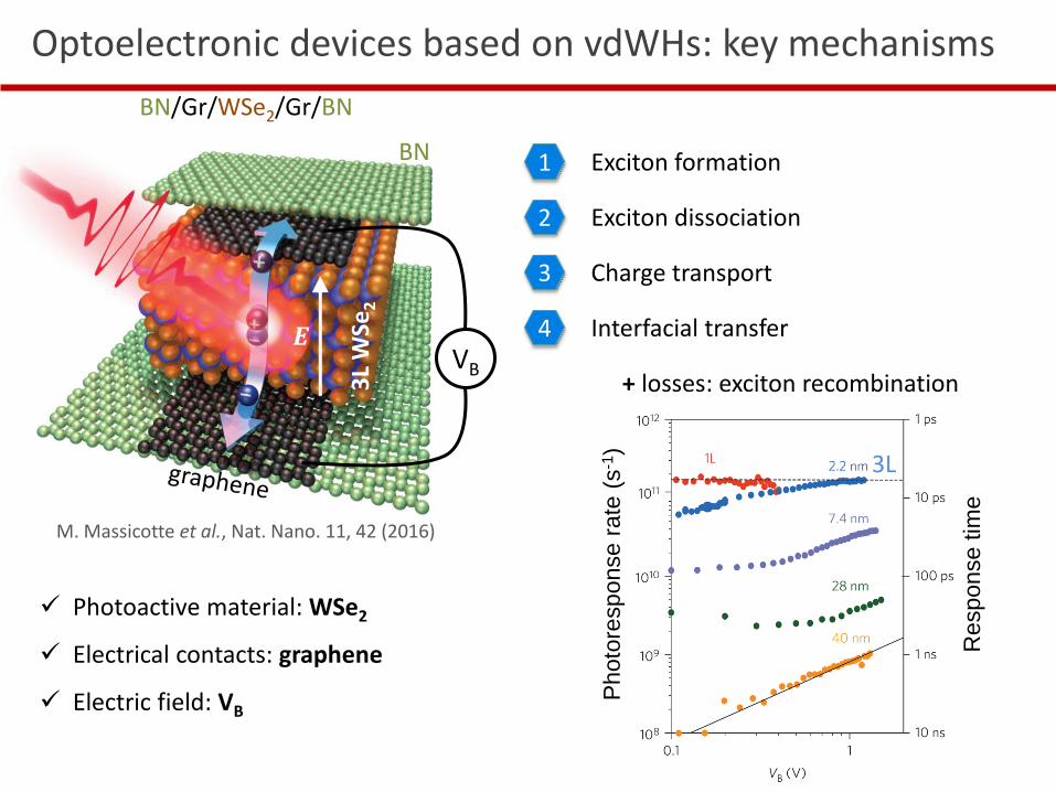
Optoelectronic devices based on vdWH: key mechanisms
BN
3L
WSe
2
BN/Gr/WSe2/Gr/BN
M. Massicotte et al., Nat. Nano. 11, 42 (2016)
Atomic dimensions ≠ conventional heterostructures
+ losses: exciton recombination
Photoactive material: WSe2
Electrical contacts: graphene
Electric field: VB
1 Exciton formation
EF EF EF
Charge transfer
Energy transfer
EF EF EF
VB 𝑬
Exciton dissociation 2
Charge transport 3
Interfacial transfer 4
Optoelectronic devices based on vdWHs: key mechanisms
BN
3L
WSe
2
BN/Gr/WSe2/Gr/BN
+ losses: exciton recombination
Photoactive material: WSe2
Electrical contacts: graphene
Electric field: VB
1 Exciton formation
VB 𝑬
Exciton dissociation 2
Charge transport 3
Interfacial transfer 4
M. Massicotte et al., Nat. Nano. 11, 42 (2016)
Photo
respo
nse
rate
(s
-1)
Re
sp
on
se
tim
e
3L
Ener
gy (
eV)
0
-4
-2
-6
-8
Cd
Se
Cd
S
Cd
Te
Mo
S 2
Mo
Se2
Mo
Te2
WS 2
WSe
2
Gra
ph
en
e
Ground state
Egap
Egap,0
dEe-e
Eopt
dEb
Band alignment and excitonic effects En
ergy
(eV
)
0
-4
-2
-6
-8
Cd
Se
Cd
S
Cd
Te
Mo
S 2
Mo
Se2
Mo
Te2
WS 2
WSe
2
Gra
ph
en
e
Ground state
Egap
Egap,0
dEe-e
Eopt
dEb
Optical Gap < Transport Gap Type I (CdSe/ZnS) or II (CdSe/CdTe) Heterojunctions
TMD: Y. Liang et al., APL 103, 42106 (2013), M. Ugeda et al., Nat. Mater. 5, 1091 (2014) Graphene: Y.-J. Yu et al., Nano Lett. 9, 3430 (2008), II-VI semicond : Norris et al. Science 2008
Data. G. Froehlicher & SB PRB 2015 See also: M. Lazzeri & F. Mauri, PRL 97, 266407 (2006) S. Pisana et al., Nat. Mat. 6, 198 (2007) J. Yan et al., PRL 98, 166802 (2007)
FvkE
= 0.031
Electron-phonon coupling and Raman spectroscopy
X ℏ𝜔𝐺
G phonon renormalization
A
G
G
FGGG E
E
EEEfEEfP
d4)(
)sgn()()(
2 202
20
)
2()
2(
4
00
0 FG
FG
GG EfEf
Data. G. Froehlicher & SB PRB 2015 See also: M. Lazzeri & F. Mauri, PRL 97, 266407 (2006) S. Pisana et al., Nat. Mat. 6, 198 (2007) J. Yan et al., PRL 98, 166802 (2007)
FvkE
= 0.031
Electron-phonon coupling and Raman spectroscopy
-300 -200 -100 0 100 200 300 400
-5.5 -2.4 -0.6 0.0 0.6 2.4 5.5 9.8
1584
1586
1588
1590
1592
1594
1596
1598
1600
1602
n (x1012
cm-2)
EF (meV)
wG (
cm
-1)
-2
0
2
4
6
8
10
12
14
DG
G (
cm
-1)
X ℏ𝜔𝐺
G phonon renormalization
Separating doping and strain
0 5 10 15 20 25
-15
-10
-5
0
5
10
15
Sample 1
Sample 2
Sample 3
Sample 4
Sample 5
2
D -
0 2D(c
m-1)
G-
0
G(cm
-1)
strain
2.22
D
G
55.02
D
G
h+
2.02
D
G
e-
Well-defined and useful correlations between Raman parameters
Data : Froehlicher & Berciaud, PRB 2015 Metten et al., PRApplied 2014 Zabel et al., Nano Lett 2012 Lee et al., Nano Lett 2012 See also : A. Das et al., Nat Nano 2008 Lee et al., Nat Comm 2012
Stra
in
Do
pin
g
0 5 10 15 20 25
0
5
10
15 electrons
holes
Sample 1
Sample 2
Sample 3
Sample 4
Sample 5
G (
cm
-1)
G (cm
-1)
0 100 200 300
0
1
2
Ra
ma
n in
ten
sity (
arb
. u
nits)
Raman shift (cm-1)
Low frequency 5 - 40 cm-1
Layer breathing mode
Layer shear mode
N = 2
𝐸𝑔 𝐸𝑢 𝐴1𝑔
𝐴2𝑢
Raman Spectrum of bilayer MoTe2
EL = 2.33 eV
0 100 200 300
0
1
2
Ra
ma
n in
ten
sity (
arb
. u
nits)
Raman shift (cm-1)
Low frequency 5 - 40 cm-1
LBM
LSM
Layer breathing mode
Layer shear mode
N = 2
𝐸𝑔 𝐸𝑢 𝐴1𝑔
𝐴2𝑢
Raman Spectrum of bilayer MoTe2
0 100 200 300
0
1
2
Ram
an inte
nsity (
arb
. units)
Raman shift (cm-1)
Mid frequency 100 - 200 cm-1
iX
oX
N = 2 iX oX
𝐸𝑔 𝐸𝑢 𝐴1𝑔
𝐴2𝑢
Raman Spectrum of bilayer MoTe2
0 100 200 300
0
1
2
Ra
ma
n in
ten
sity (
arb
. u
nits)
Raman shift (cm-1)
High frequency 200 - 300 cm-1
oMX iMX
N = 2 oMX iMX
𝐴1𝑔 𝐴2𝑢 𝐸𝑔 𝐸𝑢
Raman Spectrum of bilayer MoTe2
-50 0 50 100150200250300
0
12L MoTe
2oMX
iMX
oX
iX
Breathing
Ra
man
Inte
nsity (
arb
. un
its)
Raman Shift (cm-1)
Shear
168 172 176
2L
5L
4L
3L
1L oX mode
Ram
an Inte
nsity (
arb
. units)
Raman Shift (cm-1)
0 2 4 6 8 10 12
169
170
171
172
173
174
Fre
qu
en
cy (
cm
-1)
Number of Layers
oX
Mo Te
Interlayer interactions: Davydov splitting and unified description of the phonon modes
Froehlicher et al., Nano Lett. 15, 6481 2015 (MoTe2), Lorchat et al. ACS Nano 2016 (ReS2 and ReSe2)
Raman Spectrum of bilayer MoTe2
Luo et al., PRB 88, 075320 (2013)
Related works: • M. Grzeszczyk et al., 2D Materials 3, 25010 (2016) (MoTe2) • Q. J. Song et al., PRB 93, 115409 (2016) (MoTe2) • K. Kim et al., ACS Nano 10, 8113 (2016) (MoSe2)
Interlayer modes in van der Waals Heterostructures
• Interlayer breathing modes In TMD/TMD heterostructures
• Charge and Energy transfer In vdWH and hybrid hterostructures: MX2 + semiconductor nanostructure (nanocrystal, nanoplatelet) ANR H2DH : IPCMS, LPN, ESPCI
Spectroscopy + TRPL Time resolution down to ~1ps !
Streak Camera: an optical oscilloscope
mpip- Mainz Laquai’s group
Data from Insa Toulouse : G. Wang et al. APL 2015 & C. Robert et al. PRB 2016
MoSe2
Graphene
Quartz
Graphene
Quartz
TMD
Quartz
Outline
• Near-field coupling in hybrid heterostructures
Distance dependence Dimensionality effects
Dielectric screening Elecrical control
• Charge and energy transfer in van der Waals heterostructures
M
X
X
C MoSe2
Graphene
Graphene onMoSe2
5µm
TMD
Quartz
Nano-emitter graphene FRET
Useful for Raman studies Xie et al., JACS 2009
First theoretical studies: Swathi and Sebastian J. Chem. Phys. 2008 & 2009 Single particle studies ? Distance dependence ? Dimensionality effects ? Electrical control ?
Aptasensors Chang et al. Anal Chem 2010
Z. Chen, S. Berciaud et al. ACS Nano (2010)
Energy transfer between individual nanocrystals and graphene
• Core/shell nanocrystals on graphene : wide field fluorescence microscopy • “Proof of concept” experiment: evidence for efficient energy transfer
Graphene
Quartz
Elaser Elum
CdSe
Optical image
Graphene
Elaser Elum
CdSe
Z. Chen, S. Berciaud et al. ACS Nano (2010)
Energy transfer between individual nanocrystals and graphene
• Core/shell nanocrystals on graphene : wide field fluorescence microscopy • “Proof of concept” experiment: evidence for efficient energy transfer
Graphene
Luminescence image
Quartz
Elaser Elum
CdSe
Graphene
Elaser Elum
CdSe
Graphene
Quartz
Graphene
Quartz
Graphene Graphene
Energy transfer between individual nanocrystals and graphene
Energy transfer between individual nanocrystals and graphene
• Much faster decay on graphene and Reduced photoinduced blinking • Energy transfer efficiency > 95%
2.0 2.20
1
0 200 4001
10
2.0 2.20
1
0 50 1000
5
10
0 200 4001
10
0 50 1000
5
10
Photon energy (eV)
P
L c
ounts
(arb
. units)
0 200
Occurrence
Time delay (ns)
PL c
ounts
(arb
. units)
PL c
ounts
(arb
. units)
Photon energy (eV)
L=78 MHz
PL c
ounts
(x100 H
z)
Time (s)
0 500
Occurrence
PL c
ounts
(arb
. units)
Time delay (ns)
0 5 101
10
PL c
ounts
(x100 H
z)
Time (s)
L=1.9 MHz
g0=0.011 ns-1
g0=0.55 ns-1
F. Federspiel et al. Nano Letters 15, 1252 (2015)
Graphene
Quartz
Graphene
Quartz
0 100 2001
10
100
0 20 400
10
0 100 2001
10
100
0 20 400
10
1.8 2.00
1
1.8 2.00
1
c)
Time delay (ns)
PL c
ou
nts
(a
rb.
un
its)
e)
PL c
ou
nts
(x1
00 H
z)
Time (s)
f)
PL c
ou
nts
(a
rb.
un
its)
Time delay (ns)
0 5
10
100
b)
PL c
ou
nts
(x1
00 H
z)
Time (s)
L=3.9 MHz
L=78 MHz
Photon energy (eV)
Photon energy (eV)
PL c
ou
nts
(a
rb.
un
its) a)
d)
PL c
ou
nts
(a
rb.
un
its)
0 100
Occurence
0 100
Occurence
Graphene
Quartz
Graphene
Quartz
Energy transfer between individual nanoplatelets and graphene
• Much faster decay on graphene and Reduced photoinduced blinking • Energy transfer efficiency > 95%
F. Federspiel et al. Nano Letters 15, 1252 (2015)
Graphene
Quartz
• Mechanically exfoliated graphene monolayers on quartz
• CdSe/CdS nanocrystals (B. Dubertret, ESPCI)
• Smooth MgO films grown by MBE (D. Halley, IPCMS)
• Characterization by Raman spectroscopy and AFM
Epitaxial growth of MgO on graphene: F. Godel et al. (Nanotechnology 2013)
0 10 20 30 40 50 60 70 80 90
0.1
1
0.6 nm
2.6 nm
3.4 nm
6.0 nm
11.0 nm
17.0 nm
Co
un
ts (
arb
. u
nits)
Time delay (ns)
MgO thickness
CVD graphene
Quartz
MgO
F. Federspiel et al. Nano Letters 15, 1252 (2015)
Distance scaling of the energy transfer rate
Demonstration of a graphene-based molecular ruler (1/d4 scaling)
Swathi & Sebastian JCP 2008 & 2009 Gomez-Santos & Stauber PRB 2011 Gaudreau et al. Nano Lett 2013
D. M. Basko et al. EPJB 1999 Kos et al. PRB 2005
0D - Graphene
2D - Graphene
0 1 10 100
0.1
1
gT~1/d
4
2D-graphene model
MgO thickness (nm)
gg T
g
(ns
-1)
CVD graphene
Quartz
MgO
F. Federspiel et al. Nano Letters 15, 1252 (2015) see also arXiv:1501.03401
0
223
2
g
q
qd
T eeqdq
Dimensionality matters: platelets vs. dots
maxq
max
qd
T
qq
eqdq
0 22
23
gF
maxv
Eq
0
nm7.5Tkm
h
Bx2
4
1
dT gFor d>>1/qmax 0.3 nm q = 0 q 0 q = qmax
E0
d >> 1/qmax
Lx,Ly> and Lz<<d
Swathi & Sebastian JCP 2008 & 2009 Gomez-Santos & Stauber PRB 2011 Gaudreau et al. Nano Lett 2013
D. M. Basko et al. EPJB 1999 Kos et al. PRB 2005
0.1 1 10 1001E-6
1E-5
1E-4
1E-3
0.01
0.1
1
~d-4
~d-4
~d-3
~d-2
RE
T r
ate
gT (
arb
. u
nits)
distance (nm)
mX= 0.1 m
e
mX= 0.2 m
e
mX= 0.5 m
e
mX= m
e
mX= 1.5 m
e
~d-1
minimal distance
between graphene
and the center of the QW
dmin
~2.5 nm
measurement range
0D - Graphene
2D - Graphene
F. Federspiel et al. Nano Letters 15, 1252 (2015) see also arXiv:1501.03401
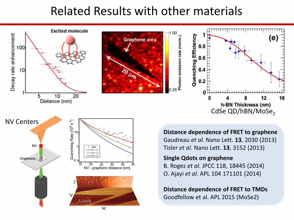
Related Results with other materials
Distance dependence of FRET to graphene Gaudreau et al. Nano Lett. 13, 2030 (2013) Tisler et al. Nano Lett. 13, 3152 (2013)
Single Qdots on graphene B. Rogez et al. JPCC 118, 18445 (2014) O. Ajayi et al. APL 104 171101 (2014) Distance dependence of FRET to TMDs Goodfellow et al. APL 2015 (MoSe2)
NV Centers
CdSe QD/hBN/MoSe2
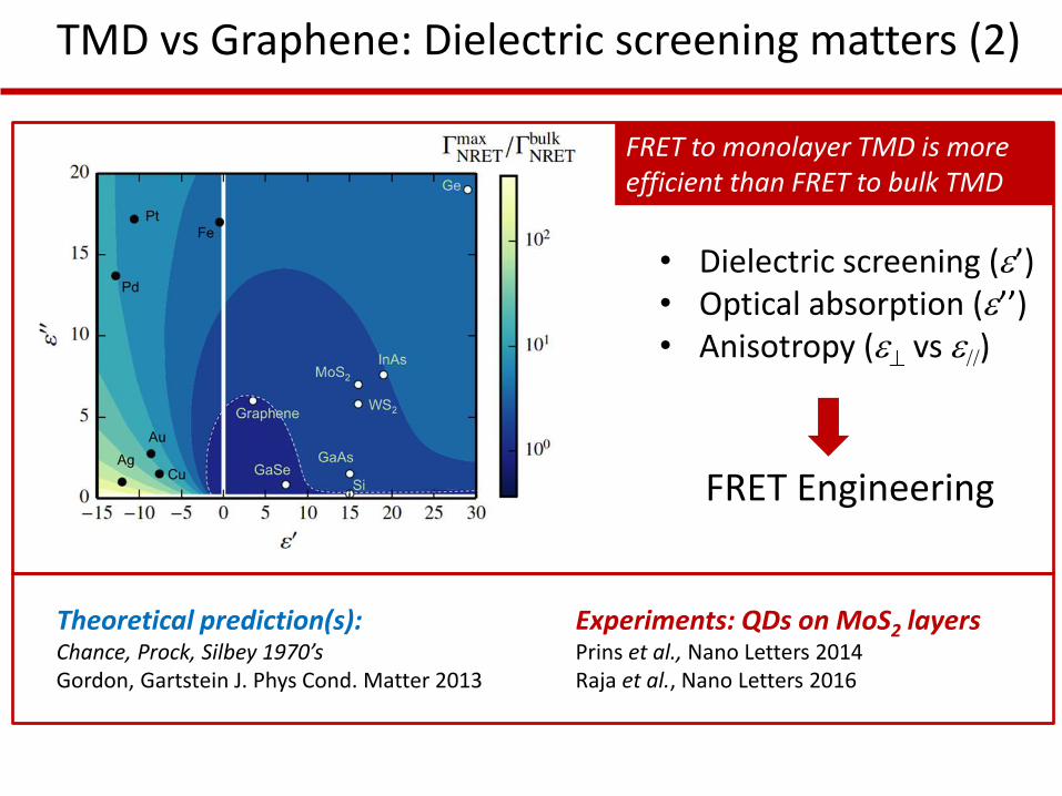
TMD vs Graphene: Dielectric screening matters (1)
Imaginary part of the dielectric constant (A)
ED(rA) depends also on epsilon and its anisotropy
Raja et al. Nano Letters 2016, see also: Z. Chen et al. ACS Nano 2010, F. Prins et al. Nano Lett 2014
FRET to monolayer TMD is more efficient than FRET to bulk TMD
• Dielectric screening (e’) • Optical absorption (e’’) • Anisotropy (e vs e)
FRET Engineering
Experiments: QDs on MoS2 layers Prins et al., Nano Letters 2014 Raja et al., Nano Letters 2016
Data: O. Zill Master’s project (2016)
TMD vs Graphene: Dielectric screening matters (2)
Quartz
Ion gelVG
Gate
Drain VSDSource
Laser
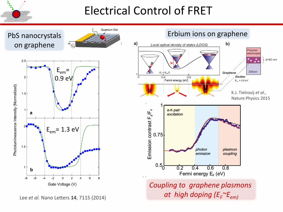
Quantum DotGraphene Hybrid phototransistors: electrical Control of FRET
Fermi Energy shifts ~ 1 eV Need for efficient gating methods
K. Tielrooij et al. Nature Physics (AOP, 2015) (Er+ ions on Graphene) See also Lee et al. Nano Letters 14, 7115 (2014) (PbS Nanocrystals on graphene)
• Electrical control of energy transfer between an ensemble of emitters and graphene State of the art: modulation of the emission rate by a factor of less than 2
x
EF<-Elum/2 EF>Elum/2
x
EF=0
Elum
Momentum
Ener
gy photoexcited
Donor
Elum FRET
Ion gel VTG
Gate
Graphene or TMD channel
Substrate (Quartz, Si/SiO2,…)
Drain Source VSD ++ + ++ +
_ _ _ ___+ + + + + +
_+
+ ++
+
__ _
__ + _
+
Paradisi et al. APL 2015
Lee et al. Nano Letters 14, 7115 (2014)
Eem= 0.9 eV
Eem= 1.3 eV
Electrical Control of FRET
Lee et al. Nano Letters 14, 7115 (2014)
PbS nanocrystals on graphene
K.J. Tielrooij et al., Nature Physics 2015
Coupling to graphene plasmons at high doping (EF~Eem)
Erbium ions on graphene
Electrical Control of FRET in QD-TMD devices
Challenges and open questions: Single particle studies Improving the modulation of the emission rate Gating efficiency? stability? reproducibility?
QD PL resonant with B exciton in MoS2 Gate-induced absorption modulation in MoS2
Gate-induced modulation of the FRET Rate
Prasai et al., Nano Lett. 2015 (K. Bolotin Group)
Raman shift (cm-1
)
VT
G (
V)
1400 1600 1800 2000 2200 2400 2600 2800
-2
0
2
4
Inte
nsity (
u.a
.)
200
400
600
800
1000
1200
G 2D
D
Beware of Polymer Electrolytes
1400 1600 2600 2800
0
1
2
before
2D
D'
G
Ra
ma
n I
nte
nsity (
a.u
.)
Raman shift (cm-1)
ID/I
G~2
after
VTG
= 0 V
1400 1600 2600 2800
2
4
6
8
10
12
p-doped
n-doped
2D
I2D
/IG 1I
D/I
G~ 1.1
ID/I
G~ 0.55
VTG
= - 2.9 V
- 1.3 V
+ 0.5 V
Ra
ma
n I
nte
nsity (
a.u
.)
Raman shift (cm-1)
+ 3 V
ID/I
G<<1
p-doped
neutral
G
Froehlicher & SB, PRB 2015
Partial conclusion
• Highly efficient « Förster-type » energy transfer (up to ~ 95%)
• Graphene-based molecular ruler at the single particle level
• Important role of dimensionality
• Electrical control : PL modulation by ~2x (graphene) up to 5x (MoS2)
• Charge transfer Photogating in Hybrid photodetectors
Outlook:
• Probing exciton dimensionality with FRET?
• Performance improvements with device engieering?
Outline
• Near-field coupling in hybrid heterostructures
Distance dependence Dimensionality effects
Dielectric screening Elecrical control
• Charge and energy transfer in van der Waals heterostructures
M
X
X
C MoSe2
Graphene
Graphene onMoSe2
5µm
TMD
Quartz
-3
-4
-5
-6
--7
Gra
ph
en
e
Mo
S 2
Mo
Se2
Mo
Te2
WS 2
WSe
2
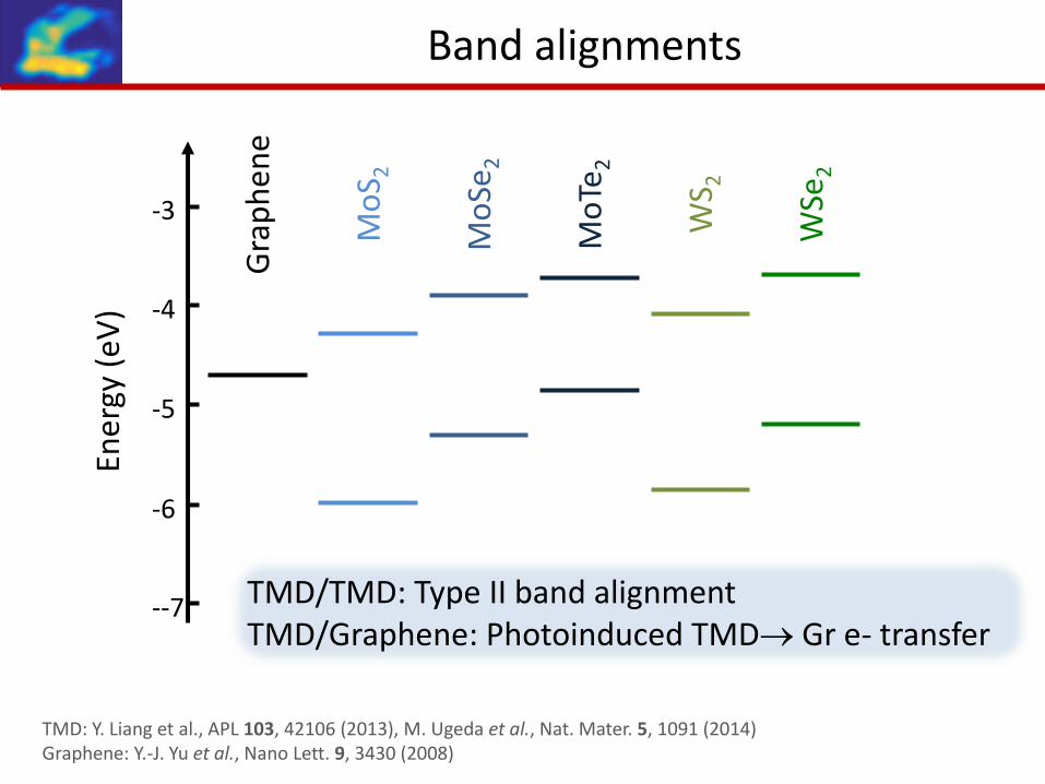
TMD: Y. Liang et al., APL 103, 42106 (2013), M. Ugeda et al., Nat. Mater. 5, 1091 (2014) Graphene: Y.-J. Yu et al., Nano Lett. 9, 3430 (2008)
-4.57
-3.89 -3.74
-4.09
-3.61
-4.29
Ene
rgy
(eV
)
TMD/TMD: Type II band alignment TMD/Graphene: Photoinduced TMD Gr e- transfer
Band alignments
Interlayer excitons in TMD/TMD heterostructures
Ultrafast (<ps) formation Long lived (>ns) Valley polarized Direct or indirect (q) PN Junctions
Schaibley et al., Nat. Rev. Materials doi:10.1038%2Fnatrevmats.2016.55
Fang et al., PNAS 2014 Hong et al., Nat Nano 2014 Lee et al., Nat Nano 2014 Rivera et al., Nat Comm 2015 Rivera et al., Science 2016 Ceballos et al., ACS Nano 2014 Ross et al., Nano Lett 2017 …
Energy Transfer in TMD/TMD heterostructures
(a)
D. Kozawa et al., Nano Lett. 2016
Open debate: competition between interlayer charge and energy transfer
Charge and energy transfer in a graphene/MoSe2
van der Waals heterostructure
Graphene + MoSe2
MoSe2
0.0 0.5 1.0 1.5
0
1
2
3
Heig
th (
nm
)
Distance (µm)
2
0.0 0.5 1.0 1.5
0
1
2
3
0.6
Heig
th (
nm
)
Distance (µm)
2
1.3 1.4 1.5 1.6 1.7 1.8 1.9
0.000
0.003
PL inte
nsity (
arb
. units)
Photon energy (eV)
1.3 1.4 1.5 1.6 1.7 1.8 1.9
0
1
PL inte
nsity (
arb
. units)
Photon energy (eV)1.3 1.4 1.5 1.6 1.7 1.8 1.9
0
1
PL
in
ten
sity (
arb
. u
nits)
Photon energy (eV)
1.3 1.4 1.5 1.6 1.7 1.8 1.9
0
1
PL inte
nsity (
arb
. units)
Photon energy (eV)
5 µm
No graphene
2 nm 0.6 nm
Decoupled Gr/MoSe2 Coupled Gr/MoSe2
Strong PL Quenching ~ 300
AFM
Photoluminescence mapping
1500 2000 25000
1
Ra
ma
n in
ten
sity (
arb
. u
nits)
Raman shift (cm-1)
2D
G
1500 2000 25000
1
Ram
an inte
nsity (
arb
. units)
Raman shift (cm-1)
G
2D
1500 2000 25000
1
Ram
an inte
nsity (
arb
. units)
Raman shift (cm-1)
G-mode frequency
No graphene
Coupled Gr/MoSe2 Decoupled Gr/MoSe2
5 µm
Raman mapping
1590 2640 2680 2720
0
1
2
3
4
52D
Ra
ma
n in
ten
sity (
arb
. u
nits)
Raman shift (cm-1)
G
1590 2640 2680 2720
0
1
2
3
Ra
ma
n in
ten
sity (
arb
. u
nits)
Raman shift (cm-1)
2DG
1590 2640 2680 2720
0
1
2
3
4
5
Ra
ma
n in
ten
sity (
arb
. u
nits)
Raman shift (cm-1)
G 2D
1590 2640 2680 2720
0
1
Ra
ma
n in
ten
sity (
arb
. u
nits)
Raman shift (cm-1)
5 µm Reference on SiO2
No graphene
Coupled Gr/MoSe2
Decoupled Gr/MoSe2
Fph increases
Eex = 2.33 eV
Raman response vs photon flux (2)
1020
1021
1022
1023
456789
13141516171819
G (
cm
-1)
Fph
(cm-2
s-1)
1020
1021
1022
1023
1584
1586
1588
1590
1592 SLG/SiO2
Decoupled SLG/MoSe2
Coupled SLG/MoSe2
G (
cm
-1)
Fph
(cm-2
s-1)
G-mode frequency G-mode FWHM
Clear signatures of photoinduced charge transfer
Raman response vs photon flux (2)
Clear signatures of photoinduced charge transfer
Raman response vs photon flux (2)
1584 1586 1588 1590 15924
6
8
10
12
14
16
18
20
G (
cm
-1)
G (cm
-1)
increasing Fph
Width-Frequency Correlation
1584 1586 1588 1590 1592
2674
2675
2676
2690
2691
2692
2693
SLG/SiO2
Decoupled SLG/MoSe2
Coupled SLG/MoSe2
2
D (
cm
-1)
G (cm
-1)
0.11
• 2D and G mode correlations: separation of strain and e-/h+ doping
𝑒− transfer
1584 1586 1588 1590 15924
6
8
10
12
14
16
18
20
G (
cm
-1)
G (cm
-1)
increasing Fph
• Comparison with Gr/MoS2
W. Zhang et al., Scientific Reports 4, 3826 (2014)
electrical measurements
𝑒− transfer
0 5 10 15 20 25
-15
-10
-5
0
5
10
15
Sample 1
Sample 2
Sample 3
Sample 4
Sample 5
2D
-
0 2D(c
m-1)
G-
0
G(cm
-1)
55.02
G
D
h+
2.02
G
D
e-
holes
electrons
Evidence for TMD Gr electron transfer
-300 -200 -100 0 100 200 3001582
1584
1586
1588
1590
1592
1594
G (
cm
-1)
EF (meV)
-300 -200 -100 0 100 200 300 400
-5.5 -2.4 -0.6 0.0 0.6 2.4 5.5 9.8
1584
1586
1588
1590
1592
1594
1596
1598
1600
1602
n (x1012
cm-2)
EF (meV)
wG (
cm
-1)
-2
0
2
4
6
8
10
12
14
DG
G (
cm
-1)
G. Froehlicher and SB, PRB 91, 205413 (2015) G. Froehlicher et al., (in preparation, 2016)
031.0Electron-phono coupling at :
Transfered electron density nG
Quantifying photoinduced doping
-300 -200 -100 0 100 200 300
4
6
8
10
12
14
16
G (
cm
-1)
EF (meV)
Saturation at EF ~ 250-300 meV Does the ICT efficiency depend on EF?
0 2 4 6 8 10 12
-200
-100
0
100
200
300
sample 1
sample 2
sample 3
EF (
me
V)
Fph
(x1023
cm-2 s
-1)
1020
1021
1022
1023
0.01
0.1
1
I PL/F
ph
oto
ns (
arb
units)
Fphotons
(cm-2 s
-1)
PL vs Fphotons
• No PL saturation on Gr/MoSe2
Drastic reduction of the excitonic lifetime (~ 1 ps) Charge and Energy Transfer?
Normalized PL: IPL
Fphotons
• PL saturation on bare and decoupled MoSe2: Exciton-Exciton Annihilation (EEA)
0 1 2 3 40.01
0.1
1
PL
co
unts
(a
rb.
un
its)
Time Delay (ns)
Graphene/MoSe2
MoSe2
IRFBare MoSe2
Decoupled Gr/MoSe2
Coupled Gr/MoSe2
EEA: N. Kumar et al., PRB 89, 125427 (2014), S. Mouri et al., PRB 90, 155449 (2014), D. Sun et al., Nano Lett. 14, 5625 (2014)
0 2 4 6 8 10 1210
-3
10-2
10-1
100
Bare MoSe2
Decoupled SLG/MoSe2
Coupled SLG/MoSe2
PL C
ounts
(arb
. units)
Time Delay (ns)
IRF
S. Mouri et al., PRB 2014
0 1 2 3 4 5
0
1
2
3
4
5
I PL (
arb
un
its)
Fph
(x1023
cm-2 s
-1)
0 1 2 3 4 5
1
2
3
4
5
nG (
x1
012 c
m-2)
Fph
(x1023
cm-2 s
-1)
Photoluminescence vs Raman
Graphene’s doping level MoSe2 PL
saturation
linear
Cannot be explained using ICT only
0 1 2 3 4 5 60
1
2
3
4
5
6
nG (
x1
01
2 c
m-2)
Fph
(x1023
cm-2 s
-1)
0 1 2 3 4 5 60
1
2
3
4
5
6
nG (
x1
01
2 c
m-2)
Fph
(x1023
cm-2 s
-1)
0 1 2 3 4 5 60
1
2
3
4
5
6
nG (
x1
01
2 c
m-2)
Fph
(x1023
cm-2 s
-1)
0 1 2 3 4 5 60
1
2
3
4
5
6
nG (
x1
01
2 c
m-2)
Fph
(x1023
cm-2 s
-1)
neutral
Toy model
CB
VB
MoSe2 graphene
+
− 𝑛G,max
ΓICT = ΓICT0 (1-nG/nG,max) X
Γ0
ΓIET
Γleaks
• At Φph = 0, 𝑛M = 0 and 𝑛G = 0
• ΓIET ≫ ΓICT, Γ0
Φphsat =
Γleaks ΓIET
ΓICT0
𝑛G,max
A
𝑛M ≈AΦph
ΓIET
𝑛G ≈𝑛G,max
1 + Φphsat Φph
Φphsat~2.5 x 1022 cm-2 s-1
Φphsat~1.25 x 1021 cm-2 s-1
air
vacuum
Γleaks ↓
𝑛G0 ≪ 𝑛G,max
MoSe2 𝑛M
𝑛G SLG
CB
VB
Γ0 ΓIET
ΓICT
Γleaks AΦph
adsorbates traps …
~ 1012 s-1
+
Efficient energy transfer from semiconductor nanostructures to 2D materials
Molecular rulers
FRET as a probe of exciton dimensionality
FRET engineering
Photoinduced e- transfer from TMD to graphene Towards local photogating of graphene
Fast IET is responsible for PL quenching
IET is more efficient than ICT
• Open questions Energy transfer mechanism in Gr-TMD? In TMD-TMD? Band alignment and excitonic effects? …
Study temperature, gate
MoSe2
Graphene
Graphene onMoSe2
5µm
Conclusion
Outlook 1: FRET-induced electrical currents
A. Brenneis et al. Nat. Nano 2015. (Holleitner group with Koppens group)
Outlook2: opto-electromechanics in 2DM
Optomechanical coupling and Raman spectroscopy in 2D resonators
D. Metten, G. Froehlicher and SB, 2D Materials 4 014004 (2017)
10 15 20 25 301E-6
1E-5
1E-4
0.001
0.01
Am
plit
ud
e (
V)
Frequency (MHz)
VG=1V
VG=-4V
2588J
Optical cryostat
VG
~
Si
SiO2
Photodiode
Am
p. (d
B)
Frequency
Spectrum analyser
2D-mode
Raman shift
G-mode
Spectrometer
Laser
Objective on PZT
Am
p. (d
B)
Frequency
Network Analyser
USIAS project: GOLEM. Collaboration: P. Verlot (ILM, Lyon) Data: K. Makles, D.Metten