Data Sheet Please read the Important Notice and Warnings at the end of this document Revision 1.0 www.infineon.com 2019-04-08 OPTIGA™ TPM SLM 9670 TPM2.0 Trusted Platform Module Data Sheet Devices • SLM 9670AQ2.0 TPM Key Features • Random Number Generator (RNG) according to NIST SP800-90A • TPM FW update functionality installed • 6962 Bytes of free NV memory • Full personalization with Endorsement Key (EK) and EK certificate • Up to 3 keys in the volatile memory • Up to 7 keys in the NV memory • Up to 8 NV counters • Support of various cryptographic algorithms – RSA-1024 and RSA-2048 – SHA-1 and SHA-256 – ECC NIST P256 – ECC BN256 Hardware Features • Qualified for industrial applications (JEDEC JESD-47) • Highly reliable flash technology with hardening extension for industrial applications • Enhanced industrial temperature range (-40..+105°C) • SPI interface up to 43 MHz • Low standby power consumption (typ. 110μA) • Supply voltage 1.8V or 3.3V • PG-VQFN-32-13 package • Pin compatible to OPTIGA TM TPM SLB9670 TPM1.2
Transcript
Data Sheet Please read the Important Notice and Warnings at the end of this document Revision 1.0www.infineon.com 2019-04-08
TPM Key Features• Random Number Generator (RNG) according to NIST SP800-90A• TPM FW update functionality installed• 6962 Bytes of free NV memory• Full personalization with Endorsement Key (EK) and EK certificate• Up to 3 keys in the volatile memory• Up to 7 keys in the NV memory• Up to 8 NV counters• Support of various cryptographic algorithms
– RSA-1024 and RSA-2048– SHA-1 and SHA-256– ECC NIST P256– ECC BN256
Hardware Features• Qualified for industrial applications (JEDEC JESD-47)• Highly reliable flash technology with hardening extension for industrial applications• Enhanced industrial temperature range (-40..+105°C)• SPI interface up to 43 MHz• Low standby power consumption (typ. 110µA)• Supply voltage 1.8V or 3.3V• PG-VQFN-32-13 package• Pin compatible to OPTIGATM TPM SLB9670 TPM1.2
Compliance and Security Features• Compliant to TPM Main Specification, Family “2.0”, Level 00, Revision 1.38• Certification according Common Criteria EAL4+• TPM2.0 compliant according to TCG test suites• Sophisticated cryptographic hardware modules (crypto processor and cryptographic engines)• Internal memory and bus encryption• Tamper-resistant secure MCU• Shielding and sensors against physical and logical attacks
About this document
Scope and purposeThis data sheet describes the OPTIGA™ TPM SLM 9670 TPM2.0 Trusted Platform Module together with itsfeatures, functionality and programming interface.
Intended audienceThis data sheet is primarily intended for system developers.
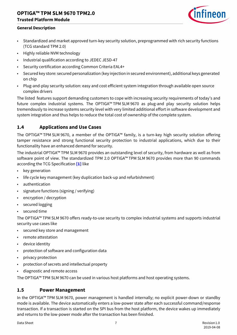
1 General DescriptionThis chapter gives a high-level overview of the OPTIGA™ TPM SLM 9670 Trusted Platform Module and its features.
1.1 OverviewThe OPTIGA™ TPM SLM 9670 (Trusted Platform Module) is a standardized security controller that protects theintegrity and authenticity of devices in industrial systems. Built on proven technologies and supporting the latestTPM 2.0 standard, the OPTIGA™ TPM SLM 9670 features include secured storage for keys, certificates andpasswords as well as dedicated key management. For details about the TCG specification, please refer towww.trustedcomputinggroup.org.To simplify system integration into hardware, the OPTIGA™ TPM SLM 9670 uses an SPI interface according to theTCG specification (see [2]). Infineon provides driver software for a simple adaptation to any standardmicrocontroller SPI interface.The TPM is a secure controller with added cryptographic functionality:• High-end security controller with advanced cryptographic algorithms implemented in hardware (for instance,
RSA-2048, ECC-256, SHA-256)• Common criteria (EAL4+) security certification• Flexible integration with SPI interface support• Extended temperature range (-40 to +105°C) for a variety of applications• Easy to integrate with wide range open source support• Unique key that identifies each TPMThe OPTIGA™ TPM SLM 9670 is a quality-hardened Trusted Platform Module (TPM) for special use in industrialapplications and based on a tamper-resistant secure microcontroller (MCU) using advanced hardware securitytechnology.As a turn-key solution, it is flashed with a securely coded firmware according to the latest TCG family 2.0specifications (see [1] and [2]) offering a rich feature set of security functions.The device is qualified according to the industrial JEDEC JESD-47 standard. It is targeting industrial applicationsrequiring a higher level of security like components of industrial automation and control systems.The OPTIGA™ TPM SLM 9670 is security certified according to Common Criteria EAL4+. It is available in a PG-VQFN-32-13 package.
1.2 Security FeaturesThe security logic consists of sophisticated features, including error detection units, a set of sensors, regulatorsand filters along with an enhanced signal shield to detect faults as well as electrical and physical conditions, andinitiate alarms to indicate security breaches.
1.3 Main Features and Customer BenefitsMain features and customer benefits of the industrial OPTIGA™ TPM SLM 9670:• Reduced risk based on proven technology• Fast time to market through concept reuse• Flexibility thanks to wide range of security functions as well as dedicated key management• Easy integration into all platform architectures and operating systems• Tamper resistant hardware architecture with performant core and peripheral set (crypto coprocessors, RNG
• Standardized and market approved turn-key security solution, preprogrammed with rich security functions (TCG standard TPM 2.0)
• Highly reliable NVM technology• Industrial qualification according to JEDEC JESD-47• Security certification according Common Criteria EAL4+• Secured key store: secured personalization (key injection in secured environment), additional keys generated
on chip• Plug-and-play security solution: easy and cost efficient system integration through available open source
complex driversThe listed features support demanding customers to cope with increasing security requirements of today’s andfuture complex industrial systems. The OPTIGA™ TPM SLM 9670 as plug-and play security solution helpstremendously to increase systems security level with very limited additional effort in software development andsystem integration and thus helps to reduce the total cost of ownership of the complete system.
1.4 Applications and Use CasesThe OPTIGA™ TPM SLM 9670, a member of the OPTIGA™ family, is a turn-key high security solution offeringtamper resistance and strong functional security protection to industrial applications, which due to theirfunctionality have an enhanced demand for security.The industrial OPTIGA™ TPM SLM 9670 provides an outstanding level of security, from hardware as well as fromsoftware point of view. The standardized TPM 2.0 OPTIGA™ TPM SLM 9670 provides more than 90 commandsaccording the TCG Specification [1] like• key generation• life cycle key management (key duplication back-up and refurbishment)• authentication• signature functions (signing / verifying)• encryption / decryption• secured logging• secured timeThe OPTIGA™ TPM SLM 9670 offers ready-to-use security to complex industrial systems and supports industrialsecurity use cases like• secured key store and management• remote attestation• device identity• protection of software and configuration data• privacy protection• protection of secrets and intellectual property• diagnostic and remote accessThe OPTIGA™ TPM SLM 9670 can be used in various host platforms and host operating systems.
1.5 Power ManagementIn the OPTIGA™ TPM SLM 9670, power management is handled internally; no explicit power-down or standbymode is available. The device automatically enters a low-power state after each successful command/responsetransaction. If a transaction is started on the SPI bus from the host platform, the device wakes up immediatelyand returns to the low-power mode after the transaction has been finished.
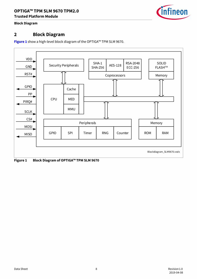
17 RST# I ST ResetExternal reset signal. Asserting this pin unconditionally resets the device. The signal is active low and is typically connected to the PCIRST# signal of the host.This pin has a weak internal pull-up resistor.
6 GPIO I/O TS GPIO-Express-00 SignalThe TPM 2.0 device does not use this functionality.This pin may be left unconnected; it has an internal pull-up resistor.
7 PP I ST Physical PresenceThe TPM2.0 device does not use this functionality.This pin may be left unconnected; it has an internal pulldown resistor.
Table 3 Power SupplyPin Number Name Pin
TypeBuffer Type
FunctionPG-VQFN-32-138, 22 VDD PWR — Power Supply
All VDD pins must be connected externally and should be bypassed to GND via 100 nF capacitors.
2, 9, 23, 32 GND GND — GroundAll GND pins must be connected externally.
Table 4 Not ConnectedPin Number Name Pin
TypeBuffer Type
FunctionPG-VQFN-32-1329, 30 NC NU — No Connect
All pins must not be connected externally (must be left floating).
3 - 5, 10 - 13, 15, 25 - 28, 31
NCI — — Not Connected InternallyAll pins are not connected internally (can be connected externally).
1 NCI/VDD — — Not Connected Internally/VDDThis pin is not connected internally (can be connected externally).Note that pin 1 is defined as VDD in the TCG specification [2]. To be compliant, VDD can be connected to this pin.
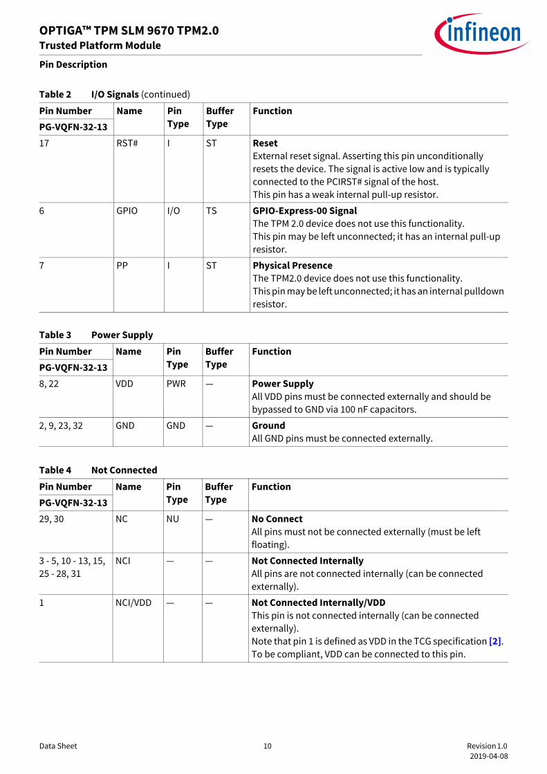
3.1 Typical SchematicFigure 3 shows the typical schematic for the OPTIGA™ TPM SLM 9670. The power supply pins should be bypassedto GND with capacitors located close to the device.
Figure 3 Typical Schematic
14 NCI/VDD — — Not Connected Internally/VDDThis pin is not connected internally (can be connected externally).Note that pin 14 is defined as VDD in the TCG specification [2]. To be compliant and to ensure upwards compatibility to future TPMs, VDD must be connected to this pin.
16 NCI/GND — — Not Connected Internally/GNDThis pin is not connected internally (can be connected externally).Note that pin 16 is defined as GND in the TCG specification [2]. To be compliant, GND can be connected to this pins.
4 TPM PropertiesAll properties defined within the TPM can be read with the command TPM2_GetCapability (capability =TPM_CAP_TPM_PROPERTIES). The values are vendor dependent or determined by a platform-specificspecification. The following properties are returned by the Infineon OPTIGA™ TPM SLM 9670:
Reading these properties returns the current version and state of the firmware. This implies that the values readback might differ from the ones shown in Table 5 above.
Table 5 Infineon Specific Property ValuesTPM_PT_MANUFACTURER “IFX”
TPM_PT_VENDOR_STRING_1 “SLM9”
TPM_PT_VENDOR_STRING_2 “670”
TPM_PT_VENDOR_STRING_3 NULL
TPM_PT_VENDOR_STRING_4 NULL
TPM_PT_FIRMWARE_VERSION_1 Major and minor version (for instance, 0x00070055 indicates V7.85)
TPM_PT_FIRMWARE_VERSION_2 Build number and Common Criteria certification state (for instance, 0x0011CB00 or 0x0011CB02)Byte 1: reserved for future use (0x00)Byte 2 and 3: Build number (for instance, 0x11CB)Byte 4: Common Criteria certification state, 0x00 means TPM is CC certified, 0x02 means TPM is not certified
5 Electrical CharacteristicsThis chapter lists the maximum and operating ranges for various electrical and timing parameters.
5.1 Absolute Maximum Ratings
Attention: Stresses above the max. values listed here may cause permanent damage to the device. Exposure to absolute maximum rating conditions for extended periods may affect device reliability. Maximum ratings are absolute ratings; exceeding only one of these values may cause irreversible damage to the integrated circuit.
5.2 Functional Operating Range
Table 6 Absolute Maximum RatingsParameter Symbol Values Unit Note or Test Condition
Min. Typ. Max.Supply Voltage VDD -0.3 – 5.0 V –
Voltage on any pin Vmax -0.3 – VDD+0.3 V –
-0.5 – VDD+0.5 V VDD = 3.3V ± 10%; pins MISO, MOSI, SCLK and CS#
Ambient temperature TA -40 – 105 °C –
Storage temperature TS -40 – 125 °C –
ESD robustness HBM:1.5 kΩ, 100 pF
VESD,HBM – – 2000 V According to EIA/JESD22-A114-B
ESD robustness VESD,CDM – – 500 V According to ESD Association Standard STM5.3.1 - 1999
Latchup immunity Ilatch 100 mA According to EIA/JESD78
Table 7 Functional Operating RangeParameter Symbol Values Unit Note or Test Condition
Min. Typ. Max.Supply Voltage VDD 3.0 3.3 3.6 V –
1.65 1.8 1.95 V –
Ambient temperature TA -40 – 105 °C –
Junction temperature Tj – – 110 °C see Section 5.3 below
As shown in Table 7, a maximum junction temperature of 110°C must not be exceeded. Thermal simulations(done using the FEM software ANSYS®) show that this temperature limit is not reached at an ambient temperatureof 105°C when the device is mounted on a PCB according to JEDEC 2s2p (JESD 51-7, JESD 51-5).If the device is mounted on a PCB compliant to JEDEC 1s0p (JESD 51-3), the simulation shows that due to self-heating of the device, the maximum junction temperature is exceeded at an ambient temperature of 105°C.
5.4 DC CharacteristicsTA = 25°C, VDD = 3.3V ± 0.3V or VDD = 1.8V ± 0.15V unless otherwise noted.
Note: Current consumption does not include any currents flowing through resistive loads on output pins!
Note: Device sleep mode will be entered after 50 milliseconds of inactivity after the last TPM command was executed.
Table 8 Thermal ResistanceParameter Symbol Values Unit Note or Test Condition
Min. Typ. Max.Junction to case Rth(JC) 35 K/W to exposed pad (bottom)1)
1) not subject to production test, specified by designJunction to ambient Rth(JA) 179 K/W 1) 2)
2) according to JEDEC JESD 51-5, JESD 51-7 at free convection and radiation on FR4 2s2p board. Board size 76.2mm x 114.3mm x 1.5mm, 2 inner copper layers (35µm), thermal via array under the exposed pad connected to the first inner copper layer. Also refer to http://www.infineon.com/cms/en/product/technology/packages/PG-VQFN
Table 9 Current ConsumptionParameter Symbol Values Unit Note or Test Condition
5.6 TimingSome pads are disabled after deassertion of the reset signal for up to 500 µs.The OPTIGA™ TPM SLM 9670 features a sophisticated protection mechanism against dictionary attacks on TPM-based authorization data. Basically, the device counts the number of failed authorization attempts in a counterwhich is located in the non-volatile memory. An attacker who has physical access to the device could try tocirumvent that mechanism by resetting the device after the authorization attempt but before the updated failurecounter has been written into the NVM.Certain countermeasures have been added to the OPTIGA™ TPM SLM 9670. In certain time windows duringpower-on or warm boot of the device, such reset events might influence the dictionary attack counters andtrigger other security mechanisms as well. In worst case, this might trigger special security defense modes fromwhich a recovery is very complex or even not possible.To avoid that the OPTIGA™ TPM SLM 9670 reaches such a security defense state, the RST# signal must not beasserted in certain time windows. After the deassertion of the RST# signal, the system should wait for a minimumtime of tRSTIN before asserting RST# again (see Figure 4 and Table 12).TPM commands should only be started after tRSTIN has expired (see Figure 4 again). If a TPM command is running,RST# should not be asserted; otherwise, this might also trigger some security functions. When the TPM shall bereset, the command TPM2_Shutdown should be issued before the assertion of the RST# signal.
MISO valid delay time tV 0 0.7 tCLKL ns Output valid delay from SCLK falling edge
MISO active time tDRV 0 ns Delay from chip select assertion to driving of MISO
Table 13 AC Characteristics of SPI Interface (continued)
Parameter Symbol Values Unit Note or Test ConditionMin. Typ. Max.
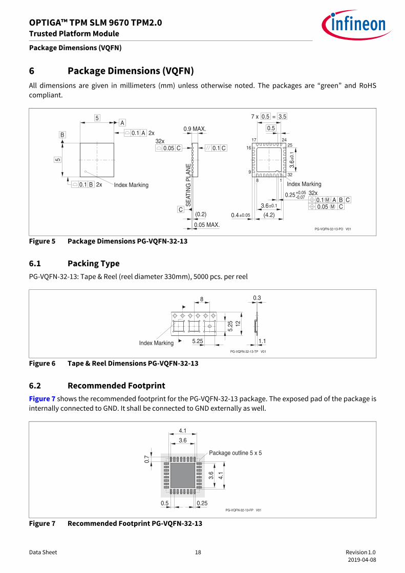
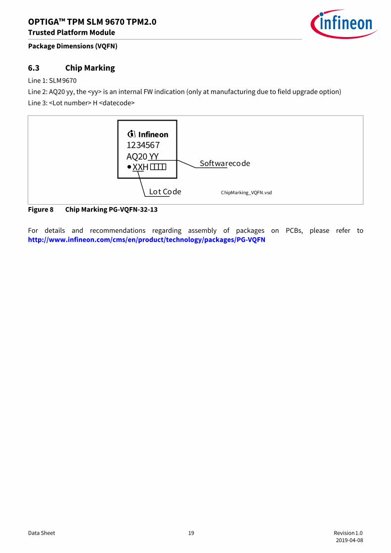
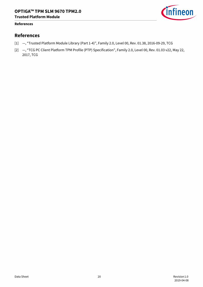
6.2 Recommended FootprintFigure 7 shows the recommended footprint for the PG-VQFN-32-13 package. The exposed pad of the package isinternally connected to GND. It shall be connected to GND externally as well.
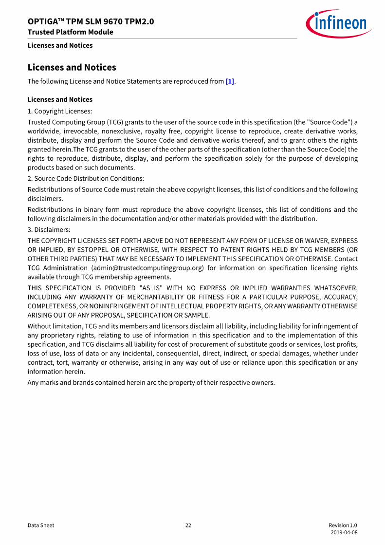
6.3 Chip MarkingLine 1: SLM9670Line 2: AQ20 yy, the <yy> is an internal FW indication (only at manufacturing due to field upgrade option)Line 3: <Lot number> H <datecode>
Figure 8 Chip Marking PG-VQFN-32-13
For details and recommendations regarding assembly of packages on PCBs, please refer tohttp://www.infineon.com/cms/en/product/technology/packages/PG-VQFN
Licenses and NoticesThe following License and Notice Statements are reproduced from [1].
Licenses and Notices1. Copyright Licenses:Trusted Computing Group (TCG) grants to the user of the source code in this specification (the "Source Code") aworldwide, irrevocable, nonexclusive, royalty free, copyright license to reproduce, create derivative works,distribute, display and perform the Source Code and derivative works thereof, and to grant others the rightsgranted herein.The TCG grants to the user of the other parts of the specification (other than the Source Code) therights to reproduce, distribute, display, and perform the specification solely for the purpose of developingproducts based on such documents.2. Source Code Distribution Conditions:Redistributions of Source Code must retain the above copyright licenses, this list of conditions and the followingdisclaimers.Redistributions in binary form must reproduce the above copyright licenses, this list of conditions and thefollowing disclaimers in the documentation and/or other materials provided with the distribution.3. Disclaimers:THE COPYRIGHT LICENSES SET FORTH ABOVE DO NOT REPRESENT ANY FORM OF LICENSE OR WAIVER, EXPRESSOR IMPLIED, BY ESTOPPEL OR OTHERWISE, WITH RESPECT TO PATENT RIGHTS HELD BY TCG MEMBERS (OROTHER THIRD PARTIES) THAT MAY BE NECESSARY TO IMPLEMENT THIS SPECIFICATION OR OTHERWISE. ContactTCG Administration ([email protected]) for information on specification licensing rightsavailable through TCG membership agreements.THIS SPECIFICATION IS PROVIDED "AS IS" WITH NO EXPRESS OR IMPLIED WARRANTIES WHATSOEVER,INCLUDING ANY WARRANTY OF MERCHANTABILITY OR FITNESS FOR A PARTICULAR PURPOSE, ACCURACY,COMPLETENESS, OR NONINFRINGEMENT OF INTELLECTUAL PROPERTY RIGHTS, OR ANY WARRANTY OTHERWISEARISING OUT OF ANY PROPOSAL, SPECIFICATION OR SAMPLE.Without limitation, TCG and its members and licensors disclaim all liability, including liability for infringement ofany proprietary rights, relating to use of information in this specification and to the implementation of thisspecification, and TCG disclaims all liability for cost of procurement of substitute goods or services, lost profits,loss of use, loss of data or any incidental, consequential, direct, indirect, or special damages, whether undercontract, tort, warranty or otherwise, arising in any way out of use or reliance upon this specification or anyinformation herein.Any marks and brands contained herein are the property of their respective owners.
Do you have a question about any aspect of this document?Email: [email protected]
IMPORTANT NOTICEThe information given in this document shall in noevent be regarded as a guarantee of conditions orcharacteristics ("Beschaffenheitsgarantie"). With respect to any examples, hints or any typicalvalues stated herein and/or any information regardingthe application of the product, Infineon Technologieshereby disclaims any and all warranties and liabilitiesof any kind, including without limitation warranties ofnon-infringement of intellectual property rights of anythird party. In addition, any information given in this document issubject to customer's compliance with its obligationsstated in this document and any applicable legalrequirements, norms and standards concerningcustomer's products and any use of the product ofInfineon Technologies in customer's applications. The data contained in this document is exclusivelyintended for technically trained staff. It is theresponsibility of customer's technical departments toevaluate the suitability of the product for the intendedapplication and the completeness of the productinformation given in this document with respect tosuch application.
For further information on technology, delivery termsand conditions and prices, please contact the nearestInfineon Technologies Office (www.infineon.com).
WARNINGSDue to technical requirements products may containdangerous substances. For information on the typesin question please contact your nearest InfineonTechnologies office.
Except as otherwise explicitly approved by InfineonTechnologies in a written document signed byauthorized representatives of Infineon Technologies,Infineon Technologies’ products may not be used inany applications where a failure of the product or anyconsequences of the use thereof can reasonably beexpected to result in personal injury.
Please read the Important Notice and Warnings at the end of this document


![OPTIGA™ TPM SLB 9670 TPM 2.0 Data Sheet · Note that pin 16 is defined as GND in the TCG specification [3]. To be compliant, GND can be connected to this pin. Data Sheet 9 Revision](https://static.documents.pub/doc/80x56/60fbd0c5f8ced305c21ac84b/optigaa-tpm-slb-9670-tpm-20-data-note-that-pin-16-is-defined-as-gnd-in-the-tcg.jpg)

![[Eng1]tpm guidebook(1 4)v1-sample_hd_trien_khai-tpm](https://static.documents.pub/doc/80x56/58eec0431a28ab3b018b45d7/eng1tpm-guidebook1-4v1-samplehdtrienkhai-tpm.jpg)


![9670 Greg Brown Presentation v1[1]](https://static.documents.pub/doc/80x56/577d22b11a28ab4e1e98028c/9670-greg-brown-presentation-v11.jpg)

