25
Optimization for Polyimide Circuit Design of Space Transformer on Probe Card Sang‐Kyu Yoo Samsung Electronics Tae‐Kyun Kim, Yong‐Ho Cho Microfriend Jong‐Kwan Yook Yonsei University
Optimization for Polyimide CircuitDesign of Space Transformer
on Probe CardSang‐Kyu YooSamsung Electronics
Tae‐Kyun Kim, Yong‐Ho ChoMicrofriend
Jong‐Kwan YookYonsei University
Overview
• Introduction of Probe Card Test• Basic Study for Polyimide Circuit Design• Signal Integrity on Probe Card• Summary• Future Works
2
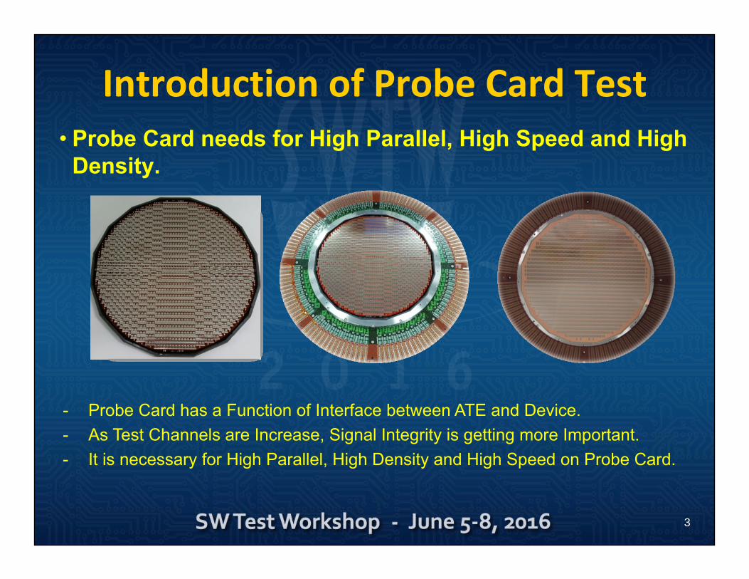
• Probe Card needs for High Parallel, High Speed and High Density.
3
Introduction of Probe Card Test
- Probe Card has a Function of Interface between ATE and Device.- As Test Channels are Increase, Signal Integrity is getting more Important.- It is necessary for High Parallel, High Density and High Speed on Probe Card.
4
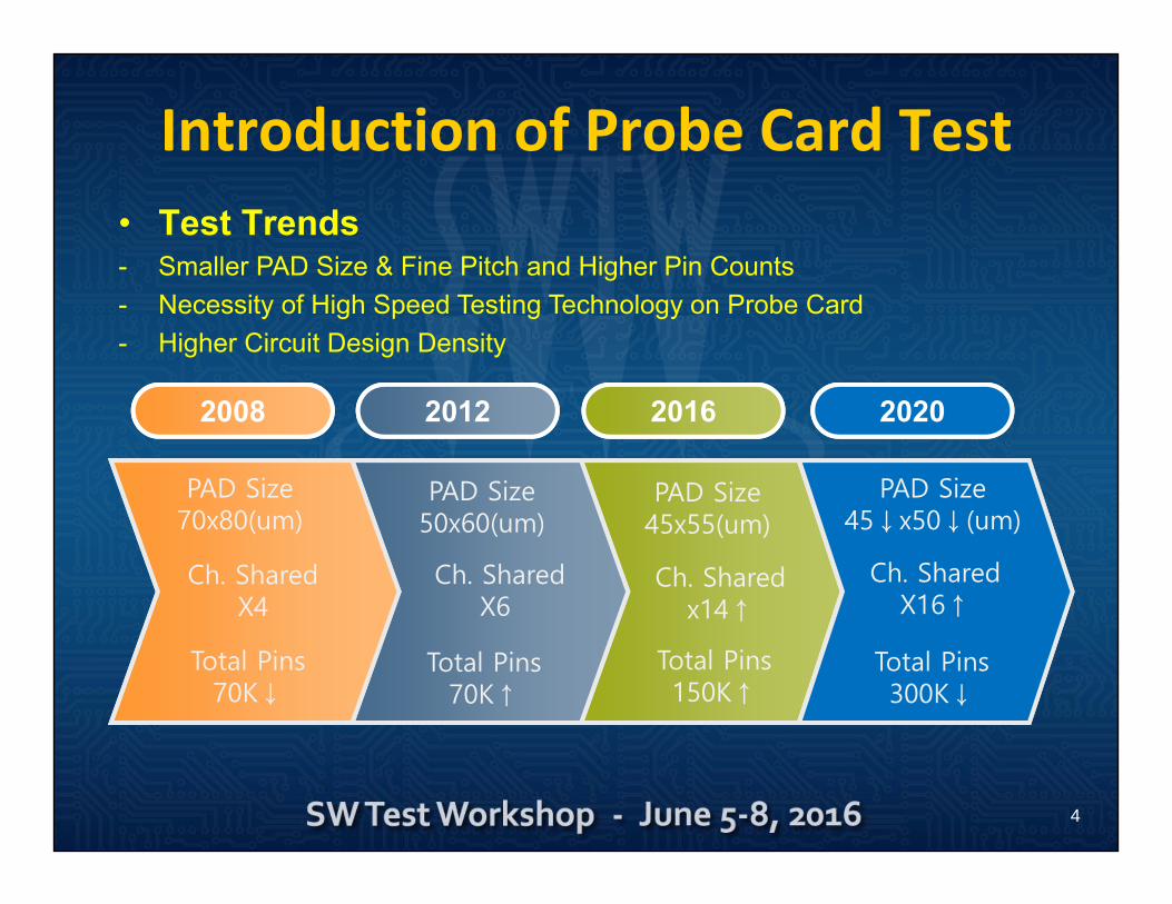
2008 2012 2016 2020
PAD Size70x80(um)
PAD Size50x60(um)
PAD Size45↓x50↓(um)
Ch. SharedX4
Ch. SharedX6
Ch. Sharedx14↑
Ch. SharedX16↑
PAD Size45x55(um)
Total Pins70K↓
Total Pins70K↑
Total Pins150K↑
Total Pins300K↓
Introduction of Probe Card Test• Test Trends- Smaller PAD Size & Fine Pitch and Higher Pin Counts- Necessity of High Speed Testing Technology on Probe Card- Higher Circuit Design Density

5
Introduction of Probe Card Test
• Advantage of Polyimide Thin Film - Very Small VIA Hole
- Highly Denser Circuit
- Low Relative Dielectric Constant
- High Propagation Velocity
- High Speed Digital Circuits
- Low Cost

6
Basic Study for PI Circuit Design• Needs for Electrical Characteristics of Circuit Trace in
Polyimide Thin Film- Dielectric Constant : 3.2- Impedance depends on Trace THK., Width, Material, Ground(Mesh & Plane)
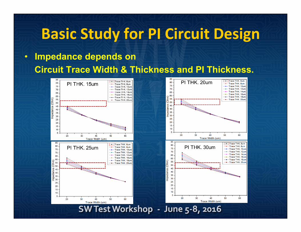
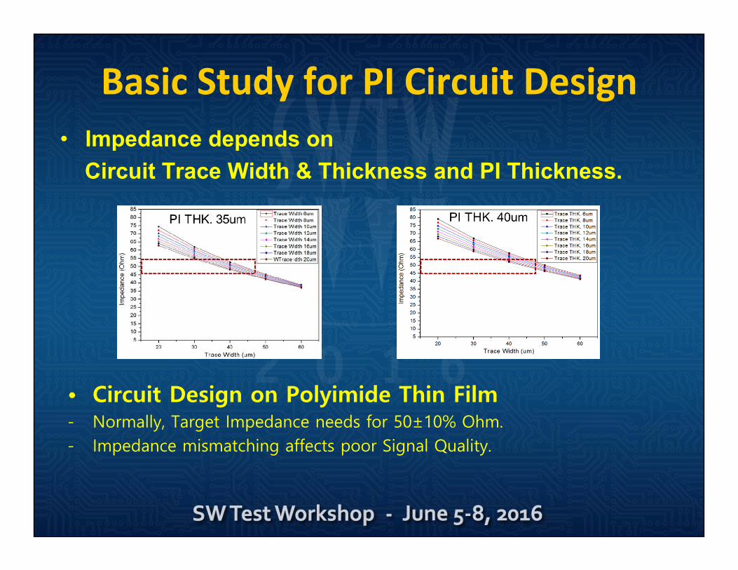
Basic Study for PI Circuit Design• Impedance depends on
Circuit Trace Width & Thickness and PI Thickness.
Basic Study for PI Circuit Design
• Circuit Design on Polyimide Thin Film- Normally, Target Impedance needs for 50±10% Ohm. - Impedance mismatching affects poor Signal Quality.
• Impedance depends on Circuit Trace Width & Thickness and PI Thickness.

0 1 2 3 4 5 615
20
25
30
35
40
45
Frequency (GHz)
Por
t Im
peda
nce
(ohm
)
MeshPlane
0 1 2 3 4 5 620
25
30
35
40
45
50
Frequency (GHz)
Por
t Im
peda
nce
(ohm
)
MeshPlane
0 1 2 3 4 5 620
30
40
50
60
70
Frequency (GHz)
Por
t Im
peda
nce
(ohm
)
MeshPlane
0 1 2 3 4 5 630
40
50
60
70
80
90
Frequency (GHz)
Por
t Im
peda
nce
(ohm
)
MeshPlane
0 1 2 3 4 5 640
50
60
70
80
90
100
110
Frequency (GHz)
Por
t Im
peda
nce
(ohm
)
MeshPlane
Basic Study for PI Circuit Design• Analysis of Impedance for Trace Material (Cu), Width
and Ground Type (Mesh or Plane)
Trace Width 30um (Cu)+ Ground Type
Trace Width 50um (Cu)+ Ground Type
Trace Width 80um (Cu)+ Ground Type
Trace Width 20um (Cu)+ Ground Type
Trace Width 100um (Cu)+ Ground Type
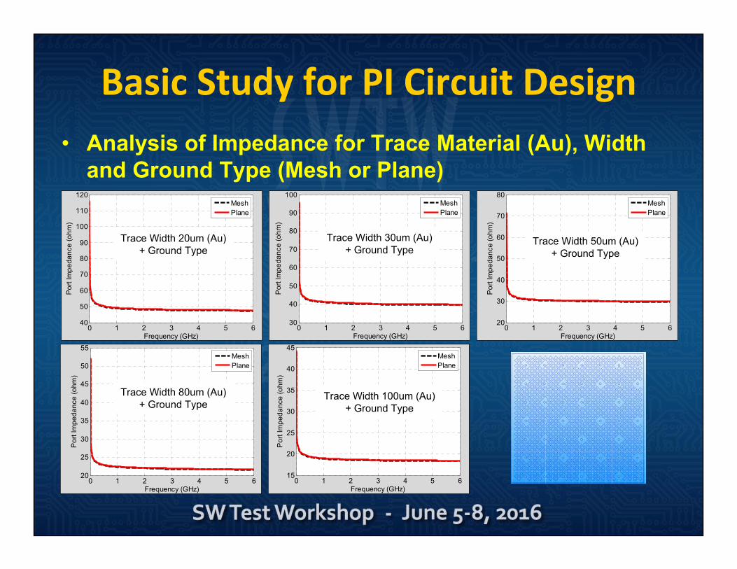
• Analysis of Impedance for Trace Material (Au), Width and Ground Type (Mesh or Plane)
Basic Study for PI Circuit Design
0 1 2 3 4 5 630
40
50
60
70
80
90
100
Frequency (GHz)
Por
t Im
peda
nce
(ohm
)
MeshPlane
Trace Width 30um (Au)+ Ground Type
0 1 2 3 4 5 620
30
40
50
60
70
80
Frequency (GHz)
Por
t Im
peda
nce
(ohm
)
MeshPlane
Trace Width 50um (Au)+ Ground Type
0 1 2 3 4 5 620
25
30
35
40
45
50
55
Frequency (GHz)
Por
t Im
peda
nce
(ohm
)
MeshPlane
Trace Width 80um (Au)+ Ground Type
0 1 2 3 4 5 640
50
60
70
80
90
100
110
120
Frequency (GHz)
Por
t Im
peda
nce
(ohm
)
MeshPlane
Trace Width 20um (Au)+ Ground Type
0 1 2 3 4 5 615
20
25
30
35
40
45
Frequency (GHz)
Por
t Im
peda
nce
(ohm
)
MeshPlane
Trace Width 100um (Au)+ Ground Type

Basic Study for PI Circuit Design• Analysis of Impedance for Circuit Trace
- Depends on Circuit Material, Width and Ground Type- Copper (Cu) vs Gold (Au)
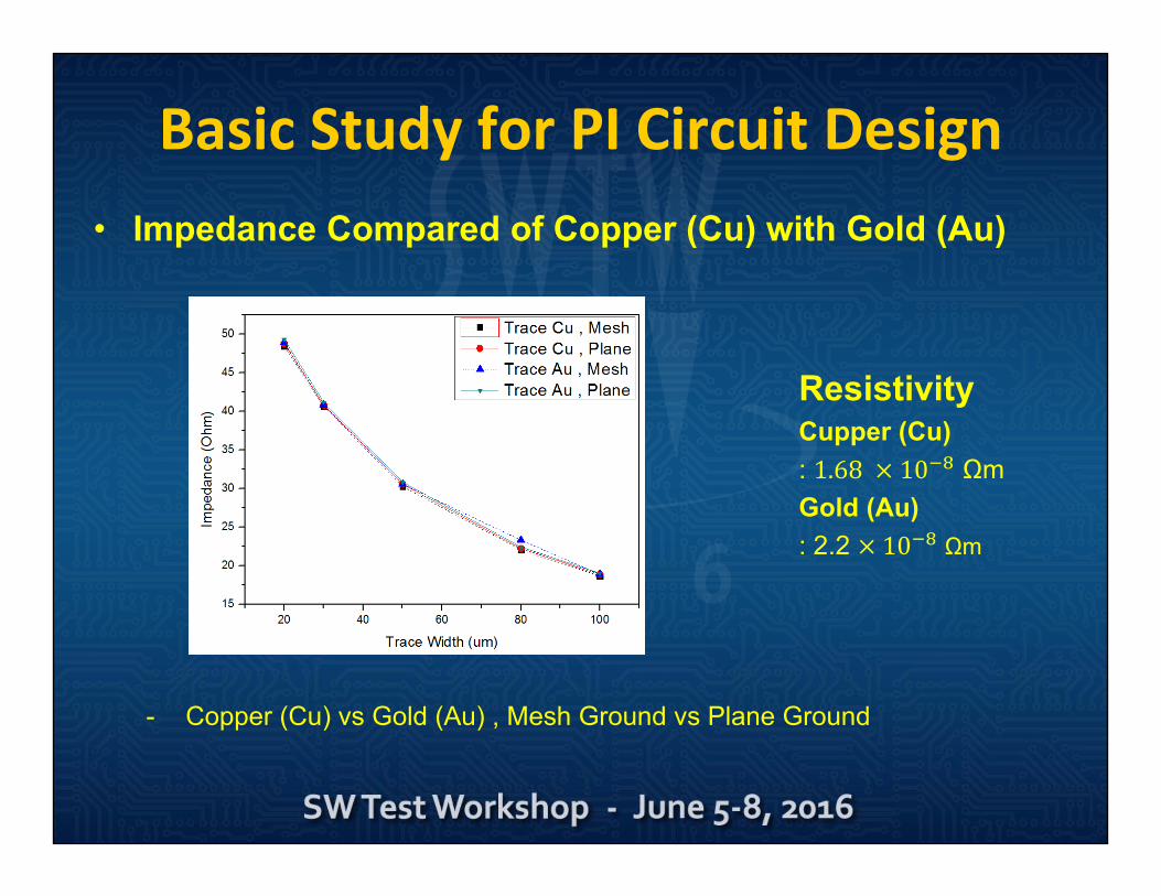
Basic Study for PI Circuit Design• Impedance Compared of Copper (Cu) with Gold (Au)
- Copper (Cu) vs Gold (Au) , Mesh Ground vs Plane Ground
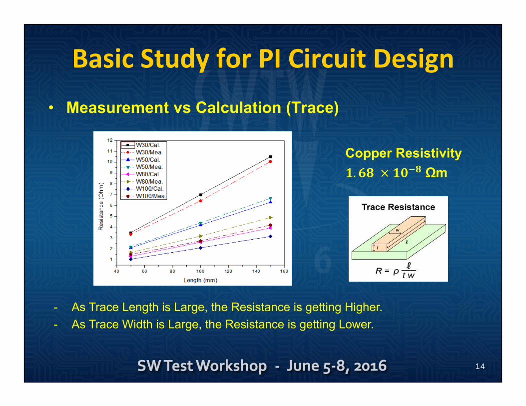
ResistivityCupper (Cu): 1.68 10 ΩmGold (Au): 2.2 10 Ωm
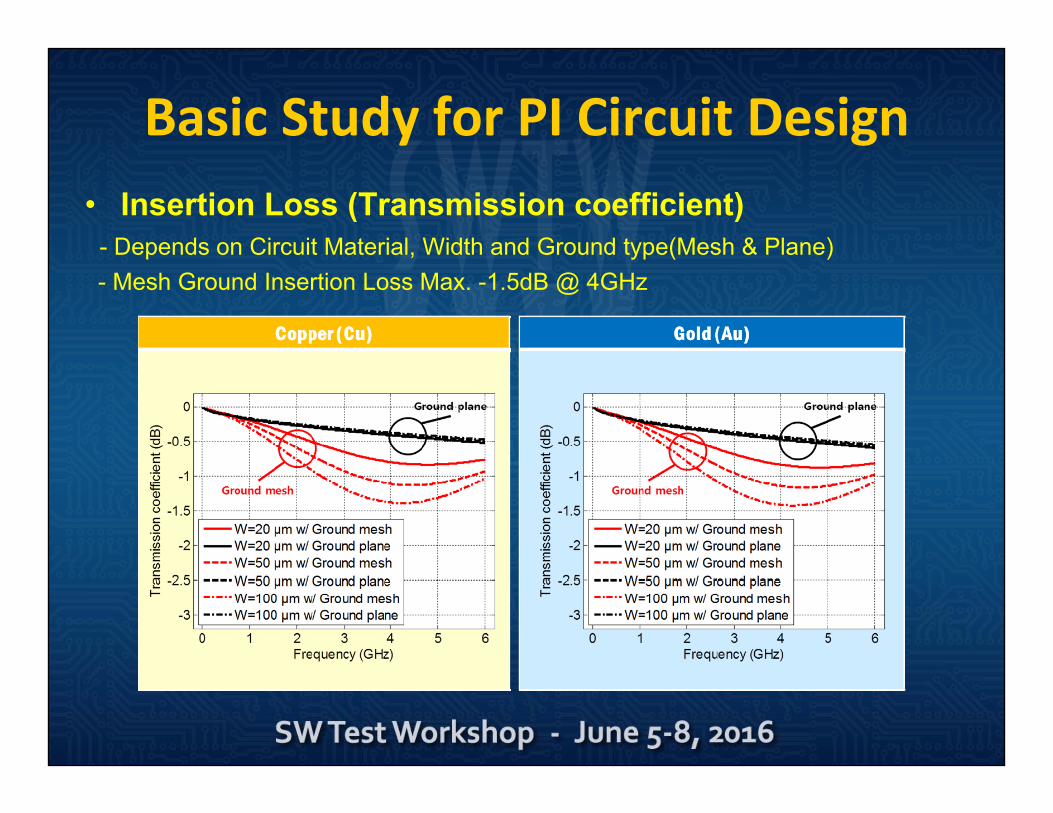
Basic Study for PI Circuit Design• Insertion Loss (Transmission coefficient)
- Depends on Circuit Material, Width and Ground type(Mesh & Plane)- Mesh Ground Insertion Loss Max. -1.5dB @ 4GHz
14
Basic Study for PI Circuit Design
Copper Resistivity. Ωm
- As Trace Length is Large, the Resistance is getting Higher.- As Trace Width is Large, the Resistance is getting Lower.
• Measurement vs Calculation (Trace)
15
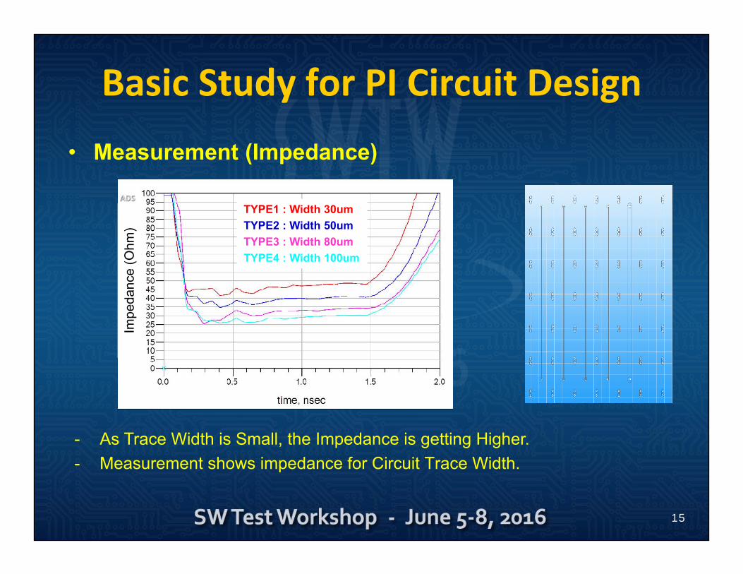
Basic Study for PI Circuit Design
- As Trace Width is Small, the Impedance is getting Higher.- Measurement shows impedance for Circuit Trace Width.
• Measurement (Impedance)
TYPE1 : Width 30umTYPE2 : Width 50umTYPE3 : Width 80umTYPE4 : Width 100um
Impe
danc
e (O
hm)
16
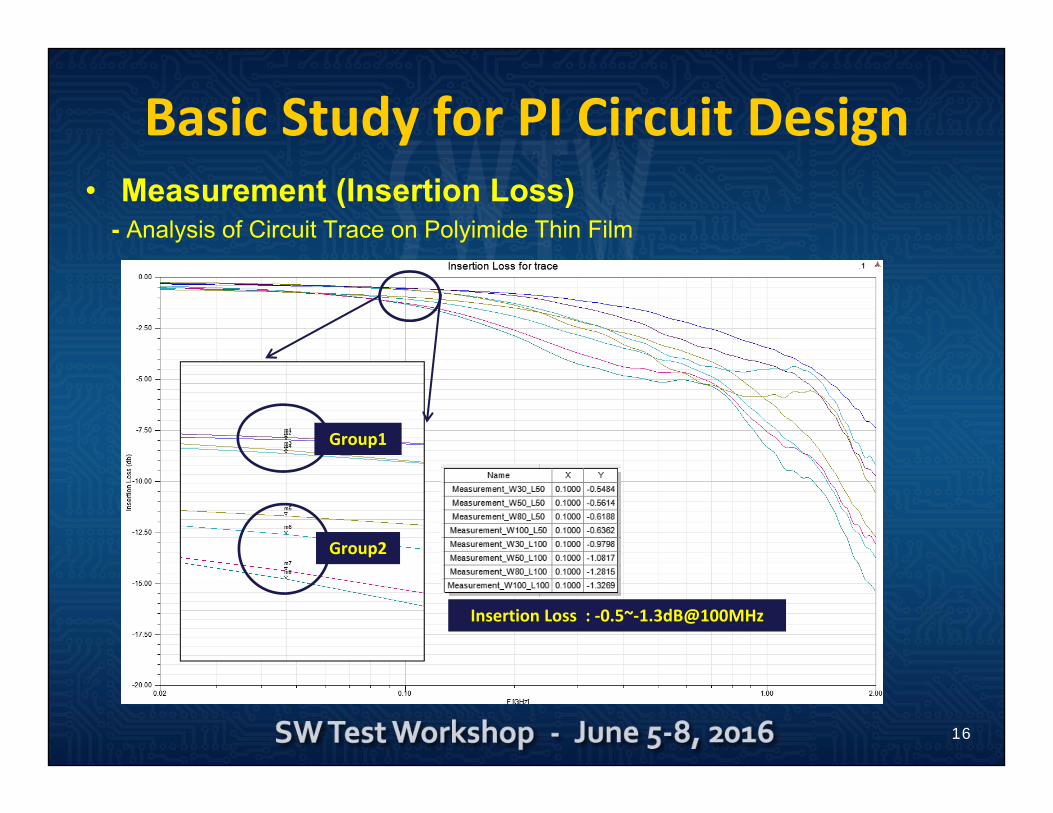
Basic Study for PI Circuit Design• Measurement (Insertion Loss)
- Analysis of Circuit Trace on Polyimide Thin Film
Insertion Loss : ‐0.5~‐1.3dB@100MHz
Group1
Group2
17
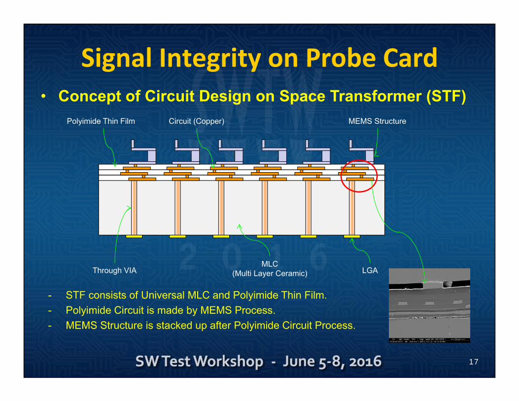
Signal Integrity on Probe Card
LGAMLC
(Multi Layer Ceramic)Through VIA
Polyimide Thin Film MEMS StructureCircuit (Copper)
- STF consists of Universal MLC and Polyimide Thin Film.- Polyimide Circuit is made by MEMS Process.- MEMS Structure is stacked up after Polyimide Circuit Process.
• Concept of Circuit Design on Space Transformer (STF)
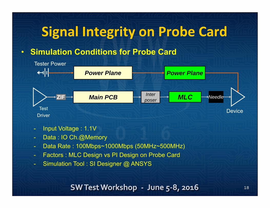
Signal Integrity on Probe Card
18
Power Plane
ZIF
Test Driver
Tester Power
Main PCB Interposer MLC Needle
Device
Power Plane
- Input Voltage : 1.1V- Data : IO Ch.@Memory- Data Rate : 100Mbps~1000Mbps (50MHz~500MHz) - Factors : MLC Design vs PI Design on Probe Card- Simulation Tool : SI Designer @ ANSYS
• Simulation Conditions for Probe Card

19
• Insertion Loss (Simulation)- Analysis of MLC Circuit Design vs PI Circuit Design on Probe Card- MLC Circuit Design -2.08dB vs PI Circuit Design -1.35dB@500MHz
PI Design
MLC Design
Signal Nets with Vias (Vias are affected by Impedance)
Signal Integrity on Probe Card
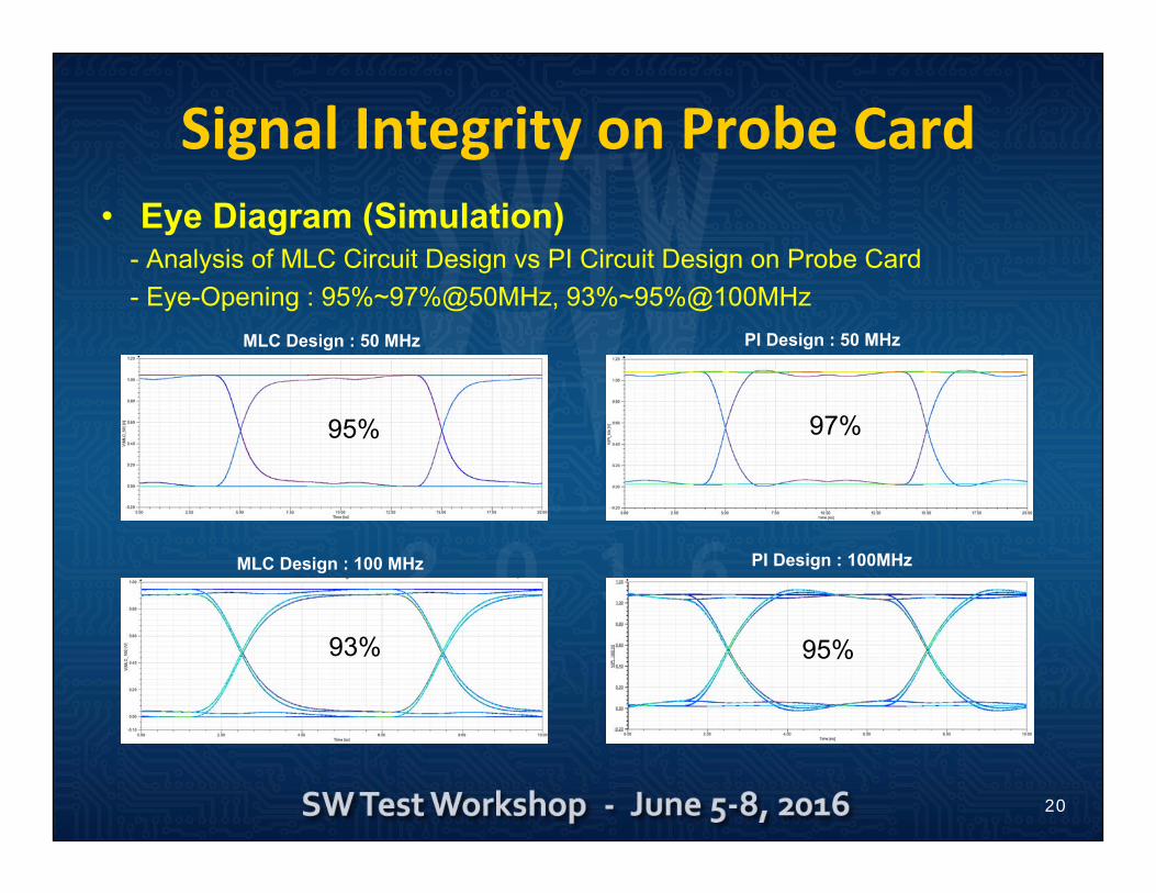
Signal Integrity on Probe Card• Eye Diagram (Simulation)
- Analysis of MLC Circuit Design vs PI Circuit Design on Probe Card- Eye-Opening : 95%~97%@50MHz, 93%~95%@100MHz
20
MLC Design : 50 MHz PI Design : 50 MHz
PI Design : 100MHzMLC Design : 100 MHz
95%
93%
97%
95%
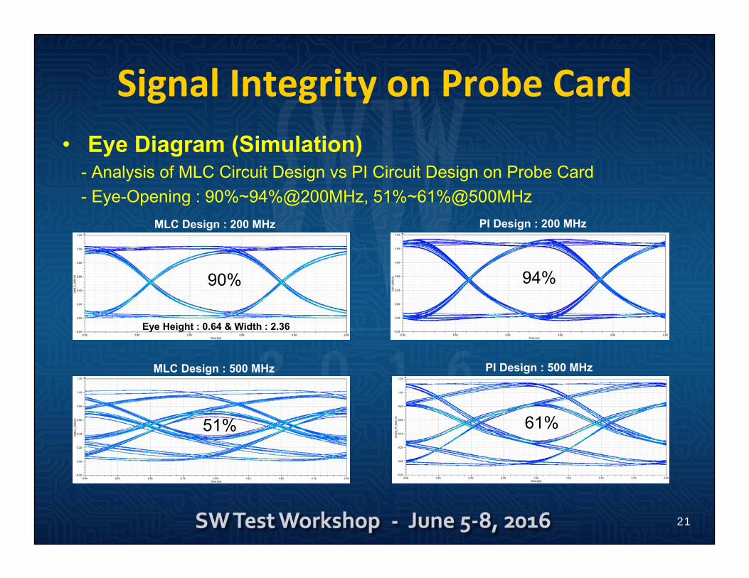
Signal Integrity on Probe Card• Eye Diagram (Simulation)
- Analysis of MLC Circuit Design vs PI Circuit Design on Probe Card- Eye-Opening : 90%~94%@200MHz, 51%~61%@500MHz
21
MLC Design : 200 MHz PI Design : 200 MHz
PI Design : 500 MHzMLC Design : 500 MHz
Eye Height : 0.64 & Width : 2.36
90%
51%
94%
61%

Summary
• Basic Study for Polyimide Circuit Design was Performed and its Electrical Characteristics have been checked.
• Impedance of Circuit Design using Polyimide Thin Film can be Controlled by changing Trace Geometry.
• Signal integrity was analyzed using two kinds of Design Concept on Probe Card.
22

Future Works
• The Electrical Characteristics for Power integrity on Probe Card
- Analysis of Power impedance using Polyimide Thin Film- Analysis of Effect for Decoupling Capacitor- Analysis of Power Noise as Ground Type(Mesh & Plane)
23
Acknowledgements
24
• Sang‐Kyu Yoo• Joon‐Yoon Kim
• Yong‐Ho Cho• Sung‐Mo Kang
• Jong‐Kwan Yook

Thanks for Your Attention !
25


