2090 IEEE TRANSACTIONS ON ELECTRON DEVICES. VOL. 37. NO. 9. SEPTEMBER 1990 Optimization of the Doping Profile in Si Permeable Base Transistors for High-Frequency , High-Voltage Operation DENNIS D. Abstract-The effects of variations in doping profiles along the di- rection of current flow in Si permeable base transistors have been in- vestigated. Numerical simulations of Poisson’s equation and the elec- tron-current-continuity equation have been used to determine the fundamental tradeoff between the unity-current-gain frequency f, and the breakdown voltage VB for a variety of doping profiles. These range from a uniform profile (4 X 10l6 cm-’) to a highly nonuniform profile in which the doping in the emitter region is greater than 100 times that in the collector region. Althoughf, decreases significantly with increas- ing collector-to-emitter voltage for the uniformly doped case, it is nearly independent of collector-to-emitter voltage for the nonuniform doping profile. In addition, nonuniform doping profiles produce devices with higher VB than uniform doping profiles for a givenf,. A class A power analysis was performed using simulated current-voltage characteris- tics, which showed that output power, power-added efficiency, and large-signal gain can be increased with devices having nonuniform doping profiles. Experimental devices with nonuniform vertical doping profiles have been fabricated using high-energy (300-400 keV) P im- plantation into a high-resistivity (44 . cm) epitaxial layer. Although present processing technology limits the f, and VB to 60% and 80% of the simulated values, respectively, an f, > 20 GHz a t a base-to-collec- tor bias of 16 V and anf, of 12 GHz at a base-to-collector bias of 26 V have been obtained. I. INTRODUCTION VARIETY of applications, including power ampli- A fiers, oscillators, and RF switches, require transis- tors exhibiting high levels of power (pulsed and CW), gain, and efficiency at high frequencies. Output power is limited by the breakdown voltage V,, gain is limited by the unity-current-gain frequency f,, and efficiency is lim- ited by both f, and V,. The usual analysis that predicts output power from the static current-voltage (Z-V) char- acteristics generally assumes that the f, of the transistor ’ exceeds the operating frequency. However, variations of f, along the load line can lead to nonlinear distortion and reduce overall gain and efficiency, particularly for class A operation. Achieving adequate V, and highf, is becom- ing increasingly important for high-speed logic circuits as well. High f;s for devices in high-speed circuit technol- ogies are normally attained by scaling both lateral and vertical device dimensions. With continued vertical scal- Manuscript received April 11, 1989; revised February 21, 1990. This work was sponsored by the Department of the Air Force. The review of this paper was arranaged by Associate Editor T. P. Chow. The author is with Lincoln Laboratory, Massachusetts Institute of Tech- nology, Lexington, MA 02173-9108. IEEE Log Number 9037183. RATHMAN ing in the future, V,’S will eventually be reduced to levels that are below present-day supply voltages [ 11. However, as Johnson [2] has pointed out, a fundamental tradeoff exists between thef, and V,, and this tradeoff is linked to material properties. Therefore, to exploit the ultimate limits of a material, one would like to simultaneously op- timize thef, and V, for a given device. One transistor that has exhibited potential in this area is the permeable base transistor (PBT) [3]-[5]. The unique feature of the PBT is the submicrometer-periodicity Schottky-barrier grating used to modulate the vertical flow of electrons. The GaAs PBT, which has a fully encapsu- lated or overgrown base region, has exhibited large gains at frequencies as high as 94 GHz [4]. The Si PBT has recently demonstrated low-phase-noise oscillator perfor- mance at fundamental frequencies as high as 22 GHz [5]. The Si version of the PBT, shown in Fig. 1, employs an etched-groove square-wave structure, in which a PtSi base grating is formed at the bottom of the grooves. It is antic- ipated that the Si PBT would have an advantage over the GaAs PBT at relatively high operating voltages because of the higher saturation velocity of Si. Combined with the higher thermal conductivity of Si, this could make the Si PBT more advantageous than the GaAs PBT at frequen- cies < 20 GHz, particularly for class A operation. The present work describes the influence of the doping profile along the direction of current flow on thefr and V, in the Si PBT. If this vertical profile is highly nonuniform (high-doped emitter, low-doped collector), the result is an f, that is nearly independent of collector bias, even for voltages near avalanche breakdown. In addition, this type of profile increases the V, of the device for a given f,. These effects are due to a large mobile space charge that is injected into the low-doped collector region. It appears likely that such nonuniform doping would enable all classes of three-terminal devices, including field-effect transistors (FET’s) high-electron-mobility transistors, and bipolar-junction transistors, to obtain larger fr V, prod- ucts. The vertical configuration of a device such as the PBT greatly simplifies the technology required to achieve nonuniform doping along the direction of current flow. 11. NUMERICAL ANALYSIS Numerical simulation is the most direct and accurate method available for modeling the PBT and related struc- 001 8-9383/90/0900-2090$01 .OO O 1990 IEEE
Transcript
2090 IEEE TRANSACTIONS ON ELECTRON DEVICES. VOL. 37. NO. 9. SEPTEMBER 1990
Optimization of the Doping Profile in Si Permeable Base Transistors for High-Frequency ,
High-Voltage Operation DENNIS D.
Abstract-The effects of variations in doping profiles along the di- rection of current flow in Si permeable base transistors have been in- vestigated. Numerical simulations of Poisson’s equation and the elec- tron-current-continuity equation have been used to determine the fundamental tradeoff between the unity-current-gain frequency f, and the breakdown voltage VB for a variety of doping profiles. These range from a uniform profile ( 4 X 10l6 cm-’) to a highly nonuniform profile in which the doping in the emitter region is greater than 100 times that in the collector region. Althoughf, decreases significantly with increas- ing collector-to-emitter voltage for the uniformly doped case, it is nearly independent of collector-to-emitter voltage for the nonuniform doping profile. In addition, nonuniform doping profiles produce devices with higher VB than uniform doping profiles for a givenf,. A class A power analysis was performed using simulated current-voltage characteris- tics, which showed that output power, power-added efficiency, and large-signal gain can be increased with devices having nonuniform doping profiles. Experimental devices with nonuniform vertical doping profiles have been fabricated using high-energy (300-400 keV) P im- plantation into a high-resistivity ( 4 4 . cm) epitaxial layer. Although present processing technology limits the f, and VB to 60% and 80% of the simulated values, respectively, a n f, > 20 GHz a t a base-to-collec- tor bias of 16 V and anf, of 12 GHz a t a base-to-collector bias of 26 V have been obtained.
I. INTRODUCTION VARIETY of applications, including power ampli- A fiers, oscillators, and RF switches, require transis-
tors exhibiting high levels of power (pulsed and CW), gain, and efficiency at high frequencies. Output power is limited by the breakdown voltage V,, gain is limited by the unity-current-gain frequency f,, and efficiency is lim- ited by both f, and V,. The usual analysis that predicts output power from the static current-voltage (Z-V) char- acteristics generally assumes that the f, of the transistor
’ exceeds the operating frequency. However, variations of f, along the load line can lead to nonlinear distortion and reduce overall gain and efficiency, particularly for class A operation. Achieving adequate V, and highf, is becom- ing increasingly important for high-speed logic circuits as well. High f;s for devices in high-speed circuit technol- ogies are normally attained by scaling both lateral and vertical device dimensions. With continued vertical scal-
Manuscript received April 11, 1989; revised February 21, 1990. This work was sponsored by the Department of the Air Force. The review of this paper was arranaged by Associate Editor T. P. Chow.
The author is with Lincoln Laboratory, Massachusetts Institute of Tech- nology, Lexington, MA 02173-9108.
IEEE Log Number 9037183.
RATHMAN
ing in the future, V,’S will eventually be reduced to levels that are below present-day supply voltages [ 11. However, as Johnson [2] has pointed out, a fundamental tradeoff exists between thef, and V,, and this tradeoff is linked to material properties. Therefore, to exploit the ultimate limits of a material, one would like to simultaneously op- timize thef, and V, for a given device.
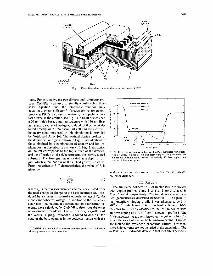
One transistor that has exhibited potential in this area is the permeable base transistor (PBT) [3]-[5]. The unique feature of the PBT is the submicrometer-periodicity Schottky-barrier grating used to modulate the vertical flow of electrons. The GaAs PBT, which has a fully encapsu- lated or overgrown base region, has exhibited large gains at frequencies as high as 94 GHz [4]. The Si PBT has recently demonstrated low-phase-noise oscillator perfor- mance at fundamental frequencies as high as 22 GHz [5]. The Si version of the PBT, shown in Fig. 1, employs an etched-groove square-wave structure, in which a PtSi base grating is formed at the bottom of the grooves. It is antic- ipated that the Si PBT would have an advantage over the GaAs PBT at relatively high operating voltages because of the higher saturation velocity of Si. Combined with the higher thermal conductivity of Si, this could make the Si PBT more advantageous than the GaAs PBT at frequen- cies < 20 GHz, particularly for class A operation.
The present work describes the influence of the doping profile along the direction of current flow on thefr and V, in the Si PBT. If this vertical profile is highly nonuniform (high-doped emitter, low-doped collector), the result is an f, that is nearly independent of collector bias, even for voltages near avalanche breakdown. In addition, this type of profile increases the V, of the device for a given f,. These effects are due to a large mobile space charge that is injected into the low-doped collector region. It appears likely that such nonuniform doping would enable all classes of three-terminal devices, including field-effect transistors (FET’s) high-electron-mobility transistors, and bipolar-junction transistors, to obtain larger fr V, prod- ucts. The vertical configuration of a device such as the PBT greatly simplifies the technology required to achieve nonuniform doping along the direction of current flow.
11. NUMERICAL ANALYSIS Numerical simulation is the most direct and accurate
method available for modeling the PBT and related struc-
001 8-9383/90/0900-2090$01 .OO O 1990 IEEE
RATHMAN: DOPING PROFILE IN Si PERMEABLE BASE TRANSISTORS 209 1
h BASE ‘AC1
I
SI02
S i02
/ PtSl
COLLECTOR \ S13N4 CONTACT
n’
Fig. I . Three-dimensional cross section of etched-emitter Si PBT
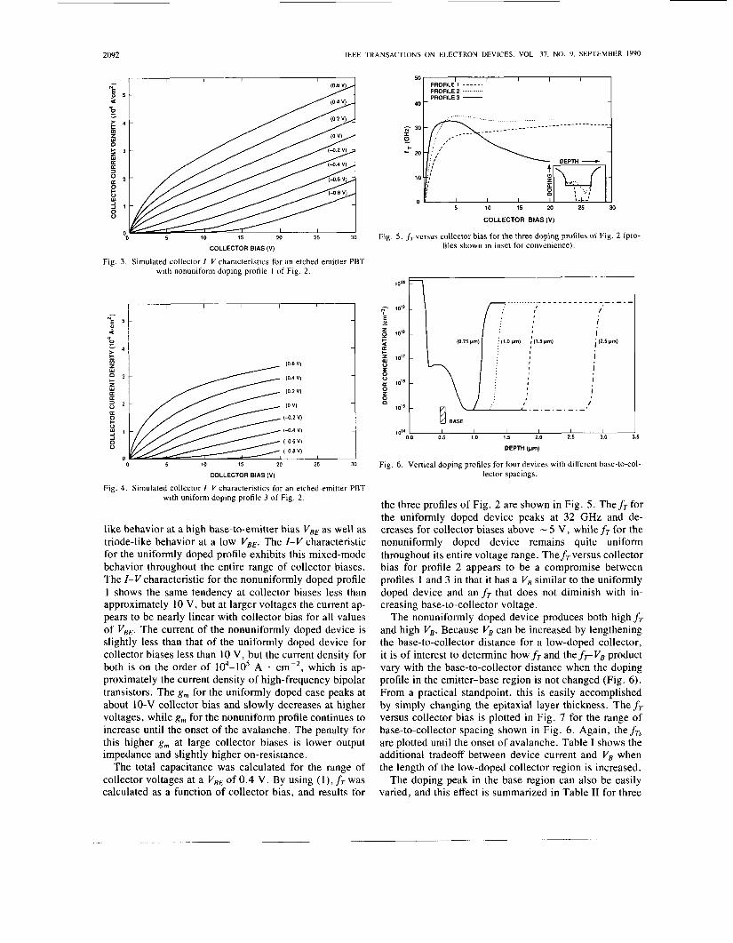
tures. For this study, the two-dimensional simulator pro- gram CANDE’ was used to simultaneously solve Pois- son’s equation and the electron-current-continuity equation to obtain collector I-V characteristics for etched- groove Si PBT’s. In these simulations, the top ohmic con- tact served as the emitter (see Fig. 1). and all devices had a 20-nm-thick base, a grating structure with 160-nm lines and spaces, and an etched-groove depth of 0.5 pm. A de- tailed description of the basic unit cell and the electrical boundary conditions used in this simulation is provided by Vojak and Alley [6]. The vertical doping profiles in the device active region, shown in Fig. 2, are identical to those obtained by a combination of epitaxy and ion im- plantation, as described in Section V. In Fig. 2, the region on the left corresponds to the top surface of the devices, and the n+ region on the right represents the heavily doped substrate. The base grating is located at a depth of 0.5 pm, which is the bottom of the etched-groove structure. From the collector I-V characteristics, the value of f T is given by
gnl
f T = 2aCT where g, is the transconductance and CT is calculated from the total change in charge on the base electrode AQT pro- duced by a change in control-electrode voltage AV,, for a constant collector voltage. In addition to the I-V char- acteristics, the maximum electron and hole ionization in- tegrals were calculated by CANDE to determine the onset of avalanche breakdown. For all devices, regardless of the vertical doping, avalanche is found to occur at the edge of the base opening in the collector region with the
‘CANDE is a numerical simulation software product of Technology Modeling Associates, Palo Alto, CA.
0.5 0.75 1.0 1.25 1.50 1.75 2.0
DEPTH (pm)
Fig. 2. Three vertical doping profiles used in PBT numerical simulations. Heavily doped regions at left and right ends of the plots constitute emitter and collector ohmic regions, respectively. The base region is the bottom of the etched groove.
avalanche voltage determined primarily by the base-to- collector distance.
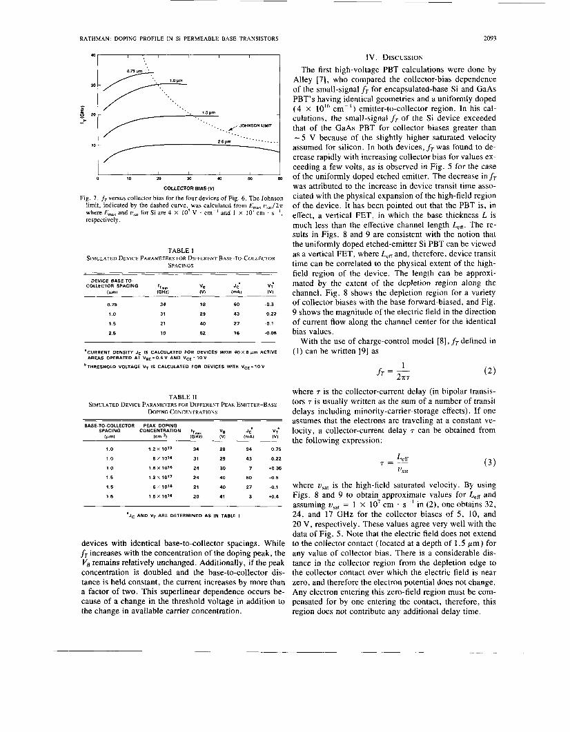
111. RESULTS The simulated collector I- V characteristics for devices
with doping profiles 1 and 3 of Fig. 2 are displayed in Figs. 3 and 4, respectively. The two devices have iden- tical geometries as described in Section 11. The peak of the nonuniform doping profile 1 was adjusted to be 1 X 10’’ cmP3, which results in a pinch-off voltage at 10-V collector bias, nearly identical to that of the device with uniform doping of 4 X lo i6 cm-3 shown in profile 3. The I-V characteristics are terminated at the collector bias for which the onset of avalanche breakdown occurs. They do not include the avalanche generation current, however, since hole currents are not included in the calculation. The Si PBT is a mixed-mode device in that it exhibits pentode-
2092 IEEE TRANSACTIONS ON ELECTRON DEVICES, VOL 37. NO. 9. SEPTEMBER 1990
50
40
I I I I I N
5 5 -
-5 a
5 10 15 20 25 30
I I I I I PROFILE1
PROFILE 3 - PROFILE 2 ...........
- -
COLLECTOR BIAS (V)
Fig. 3. Simulated collector I -V characteristics for an etched-emitter PBT with nonunifom doping profile 1 of Fig. 2.
I I I I I
f
0 5 10 15 20
COLLECTOR BIAS (V)
Fig. 4. Simulated collector I -V characteristics for an etched-emitter PBT with uniform doping profile 3 of Fig. 2 .
like behavior at a high base-to-emitter bias V,, as well as triode-like behavior at a low VBE. The I-V characteristic for the uniformly doped profile exhibits this mixed-mode behavior throughout the entire range of collector biases. The I- V characteristic for the nonuniformly doped profile 1 shows the same tendency at collector biases less than approximately 10 V, but at larger voltages the current ap- pears to be nearly linear with collector bias for all values of VBE. The current of the nonuniformly doped device is slightly less than that of the uniformly doped device for collector biases less than 10 V, but the current density for both is on the order of 104-105 A - cmP2, which is ap- proximately the current density of high-frequency bipolar transistors. The g, for the uniformly doped case peaks at about 10-V collector bias and slowly decreases at higher voltages, while g, for the nonuniform profile continues to increase until the onset of the avalanche. The penalty for this higher g, at large collector biases is lower output impedance and slightly higher on-resistance.
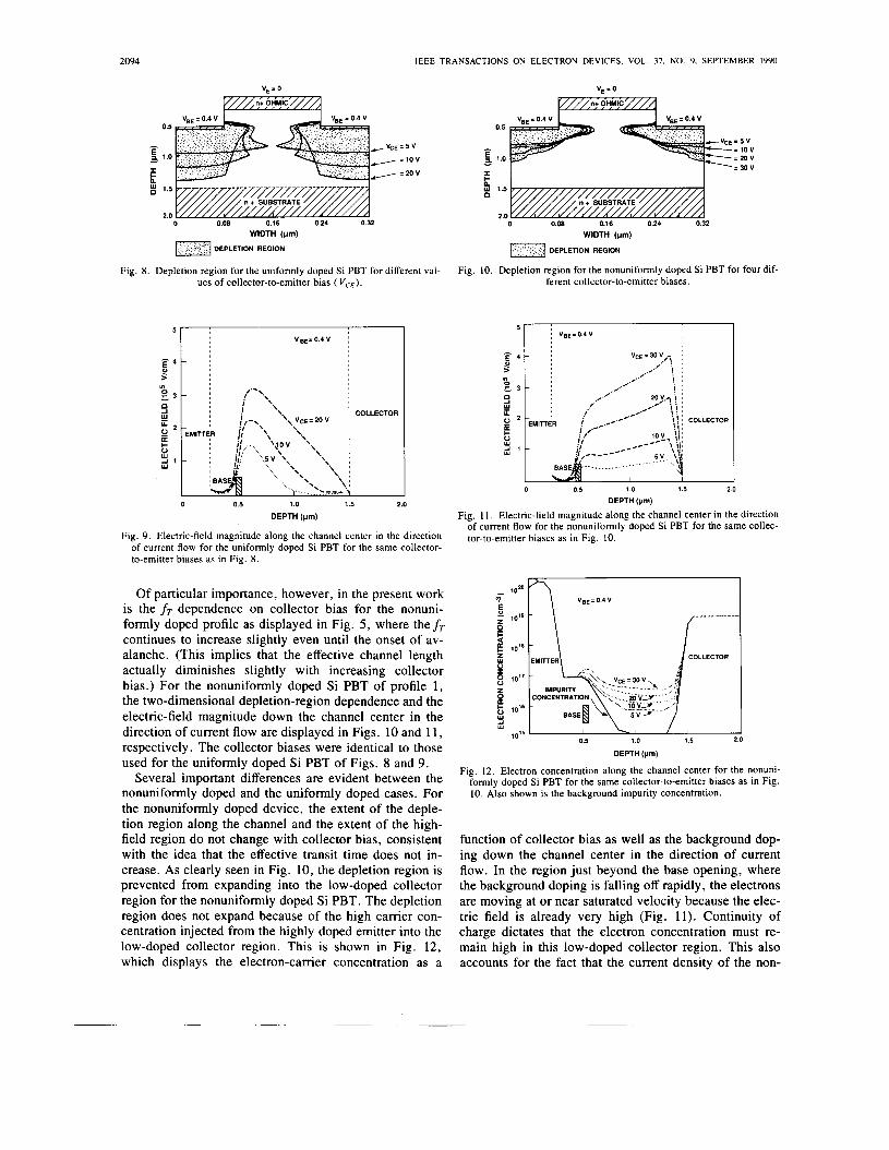
The total capacitance was calculated for the range of collector voltages at a V,, of 0.4 V. By using ( l ) , fT was calculated as a function of collector bias, and results for
Fig. 5 . fT versus collector bias for the three doping profiles of Fig. 2 (pro- files shown in inset for convenience).
-.- / *
I I ; (2.5 vm)
I I I I ; -.-.-
I I I I I I
DEPTH (pm)
3.0 1.5 2.0 2.5 0.0 0.5 1 .o 5
Fig. 6 . Vertical doping profiles for four devices with different base-to-col- lector spacings.
the three profiles of Fig. 2 are shown in Fig. 5 . ThefT for the uniformly doped device peaks at 32 GHz and de- creases for collector biases above - 5 V, while f T for the nonuniformly doped device remains quite uniform throughout its entire voltage range. ThefT versus collector bias for profile 2 appears to be a compromise between profiles 1 and 3 in that it has a V , similar to the uniformly doped device and an f T that does not diminish with in- creasing base-to-collector voltage.
The nonuniformly doped device produces both high fT and high V,. Because V, can be increased by lengthening the base-to-collector distance for a low-doped collector, it is of interest to determine how f T and thefrV, product vary with the base-to-collector distance when the doping profile in the emitter-base region is not changed (Fig. 6 ) . From a practical standpoint, this is easily accomplished by simply changing the epitaxial layer thickness. The f T versus collector bias is plotted in Fig. 7 for the range of base-to-collector spacing shown in Fig. 6 . Again, the fTs are plotted until the onset of avalanche. Table I shows the additional tradeoff between device current and Vs when the length of the low-doped collector region is increased.
The doping peak in the base region can also be easily varied, and this effect is summarized in Table I1 for three
RATHMAN: DOPING PROFILE IN Si PERMEABLE BASE TRANSISTORS 2093
1 . 1 I I I 40
30 - 9- - 2 '.. 1.5pm
c I- - . . . . . . r / JOHNSON LIMIT
0 20 -
-. .. - . - - . .___
< * .
2.5 prn 10 -
I I I I I
IV. DISCUSSION The first high-voltage PBT calculations were done by
Alley [7], who compared the collector-bias dependence of the small-signal f r for encapsulated-base Si and GaAs PBT's having identical geometries and a uniformly doped ( 4 x 10I6 ~ m - ~ ) emitter-to-collector region. In his cal-
that of the GaAs PBT for collector biases greater than -5 V because of the slightly higher saturated velocity assumed for silicon. In both devices, f T was found to de- crease rapidly with increasing collector bias for values ex- ceeding a few volts, as is observed in Fig. 5 for the case
culations, the small-signal fT of the Si device exceeded
'CURRENT DENSITY J~ IS CALCULATED FOR DEVICES WITH 4 0 X 8 p m ACTIVE
b~~~~~~~~~ VOLTAGE vT IS CALCUIATED FOR DEVICES WITH vCE = i o v
(1) can be written [9] as AREAS OPERATED AT VBE = 0 . 4 V AND VcE = 10 V
1 fT =
0 10 20 30 40 50 M) of the uniformly doped etched emitter. The decrease infr
where 7 is the collector-current delay (in bipolar transis-
delays including minority-camer-storage effects). If one assumes that the electrons are traveling at a constant ve-
SPACING CONCENTRATION fT,,, V0 JC' v; locity, a collector-current delay 7 can be obtained from the following expression:
TABLE I1 SIMULATED DEVICE PARAMETERS FOR DIFFERENT PEAK EMITTER-BASE tors is usually written as the sum Of a number Of transit
DOPING CONCENTRATIONS
EASE-TO-COLLECTOR PEAK DOPING
WmI (cm-31 IGHzI IVI (mAl (VI
1 .o 1.2 x 10¹⁷ 3 4 28 9 4 -0.75
1 .o 6 X 10¹⁶ 31 29 43 -0.22
1 .0 1.5 X 1 0 l 6 24 30 7 + 0 3 5
1.5 1 . 2 ~ 1 0 1 7 24 40 50 -0.5
1.5 6 X 10¹⁶ 21 4 0 27 -0.1
1.5 1.5 X 1 0 l 6 20 41 3 t 0 . 4
*Jc AND VT ARE DETERMINED AS IN TABLE I
devices with identical base-to-collector spacings. While fT increases with the concentration of the doping peak, the VB remains relatively unchanged. Additionally, if the peak concentration is doubled and the base-to-collector dis- tance is held constant, the current increases by more than a factor of two. This superlinear dependence occurs be- cause of a change in the threshold voltage in addition to the change in available carrier concentration.
( 3 ) Leff Vsat
7 = -
where usat is the high-field saturated velocity. By using Figs. 8 and 9 to obtain approximate values for Le, and assuming usat = 1 x lo7 cm - s-I in (2), one obtains 32, 24, and 17 GHz for the collector biases of 5, 10, and 20 V, respectively. These values agree very well with the data of Fig. 5. Note that the electric field does not extend to the collector contact (located at a depth of 1.5 pm) for any value of collector bias. There is a considerable dis- tance in the collector region from the depletion edge to the collector contact over which the electric field is near zero, and therefore the electron potential does not change. Any electron entering this zero-field region must be com- pensated for by one entering the contact, therefore, this region does not contribute any additional delay time.
2094 IEEE TRANSACTIONS ON ELECTRON DEVICES. VOL. 37. NO. 9. SEPTEMBER 1990
v E = o
n+ OHMIC/
0 5
- - VCE = 5 v / = 1 o v f 1 0
z / .2ov - t -
1.5
2.0 0 0.08 0.16 0.24 0.32
WIDTH (pm)
-1 DEPLETION REGION
Fig. 8. Depletion region for the uniformly doped Si PBT for different val- ues of collector-to-emitter bias ( VCE).
COLLECTOR
0 0.5 1 .o 1.5 2.0
DEPTH (pm)
Fig. 9. Electric-field magnitude along the channel center in the direction of current flow for the uniformly doped Si PBT for the same collector- to-emitter biases as in Fig. 8.
Of particular importance, however, in the present work is the fT dependence on collector bias for the nonuni- formly doped profile as displayed in Fig. 5 , where thefT continues to increase slightly even until the onset of av- alanche. (This implies that the effective channel length actually diminishes slightly with increasing collector bias.) For the nonuniformly doped Si PBT of profile 1, the two-dimensional depletion-region dependence and the electric-field magnitude down the channel center in the direction of current flow are displayed in Figs. 10 and 11, respectively. The collector biases were identical to those used for the uniformly doped Si PBT of Figs. 8 and 9.
Several important differences are evident between the nonuniformly doped and the uniformly doped cases. For the nonuniformly doped device, the extent of the deple- tion region along the channel and the extent of the high- field region do not change with collector bias, consistent with the idea that the effective transit time does not in- crease. As clearly seen in Fig. 10, the depletion region is prevented from expanding into the low-doped collector region for the nonuniformly doped Si PBT. The depletion region does not expand because of the high carrier con- centration injected from the highly doped emitter into the low-doped collector region. This is shown in Fig. 12, which displays the electron-carrier concentration as a
VE.O
/n+ OHMIC’
0 5
= 5 v - = 1 o v
.3ov f 1 0 = 20 v - E 4 1 5 0
2 0 0 008 0.16 0 24 0 32
WIDTH (pm)
DEPLETION REGION
Fig. 10. Depletion region for the nonuniformly doped Si PBT for four dif- ferent collector-to-emitter biases
COLLECTOR
0 0.5 1 .o 1.5 2
DEPTH (pm)
Fig. 11. Electric-field magnitude along the channel center in the direction of current flow for the nonuniformly doped Si PBT for the same collec- tor-to-emitter biases as in Fig. 10.
i? VBE= 0.4 V
0.5 1 .o 1.5
DEPTH (pm)
Fig. 12. Electron concentration along the channel center for the nonuni- formly doped Si PBT for the same collector-to-emitter biases as in Fig. 10. Also shown is the background impurity concentration.
function of collector bias as well as the background dop- ing down the channel center in the direction of current flow. In the region just beyond the base opening, where the background doping is falling off rapidly, the electrons are moving at or near saturated velocity because the elec- tric field is already very high (Fig. 11). Continuity of charge dictates that the electron concentration must re- main high in this low-doped collector region. This also accounts for the fact that the current density of the non-
RATHMAN: DOPING PROFILE IN Si PERMEABLE BASE TRANSISTORS 2095
uniformly doped device (see Figs. 3 and 4) is not signif- icantly diminished by the low-doped collector region.
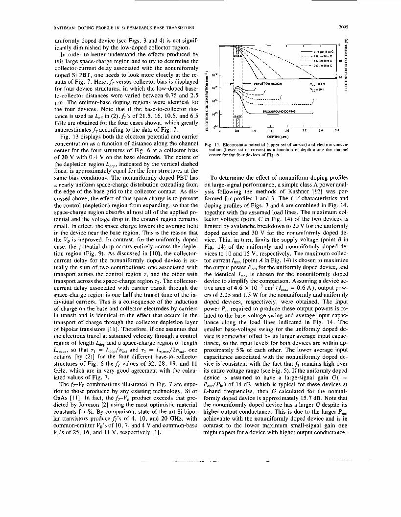
In order to better understand the effects produced by this large space-charge region and to try to determine the collector-current delay associated with the nonuniformly doped Si PBT, one needs to look more closely at the re- sults of Fig. 7. Here, fr versus collector bias is displayed for four device structures, in which the low-doped base- to-collector distances were varied between 0.75 and 2.5 pm. The emitter-base doping regions were identical for the four devices. Note that if the base-to-collector dis- tance is used as Le# in (2),f,'s of 21.5, 16, 10.5, and 6.5 GHz are obtained for the four cases shown, which greatly underestimates fr according to the data of Fig. 7.
Fig. 13 displays both the electron potential and carrier concentration as a function of distance along the channel center for the four strutures of Fig. 6 at a collector bias of 20 V with 0.4 V on the base electrode. The extent of the depletion region Ldep, indicated by the vertical dashed lines, is approximately equal for the four structures at the same bias conditions. The nonuniformly doped PBT has a nearly uniform space-charge distribution extending from the edge of the base grid to the collector contact. As dis- cussed above, the effect of this space charge is to prevent the control (depletion) region from expanding, so that the space-charge region absorbs almost all of the applied po- tential and the voltage drop in the control region remains small. In effect, the space charge lowers the average field in the device near the base region. This is the reason that the V, is improved. In contrast, for the uniformly doped case, the potential drop occurs entirely across the deple- tion region (Fig. 9). As discussed in [lo], the collector- current delay for the nonuniformly doped device is ac- tually the sum of two contributions: one associated with transport across the control region r , and the other with transport across the space-charge region r2. The collector- current delay associated with carrier transit through the space-charge region is one-half the transit time of the in- dividual carriers. This is a consequence of the induction of charge on the base and collector electrodes by carriers in transit and is identical to the effect that occurs in the transport of charge through the collector depletion layer of bipolar transistors [ 1 11. Therefore, if one assumes that the electrons travel at saturated velocity through a control region of length Ldep and a space-charge region of length
obtains [by (2)] for the four different base-to-collector structures of Fig. 6 the fr values of 32, 28, 19, and 11 GHz, which are in very good agreement with the calcu- lated values of Fig. 7.
ThefrVe combinations illustrated in Fig. 7 are supe- rior to those produced by any existing technology, Si or GaAs [ l l ] . In fact, the frVe product exceeds that pre- dicted by Johnson [2] using the most optimistic material constants for Si. By comparison, state-of-the-art Si bipo- lar transistors producef,'~ of 4, 10, and 20 GHz, with common-emitter V,'s of 10, 7, and 4 V and common-base VB's of 25, 16, and 11 V, respectively [I].
Lspace, so that 71 = Ldep/Vsat and 7 2 = Lspace/2Vsatr one
- 5. 5 5
I I I 0 - l
- 0.75 prn B IO c ---- 1.0prnBtoC 1.5prnBtoC - 10 2.5prn BIOC 2
a
._ - - - - - - '. -. \.
v)
- " g i
'. '. '. '. '. - 1 - 5 2 1017 - a
5 10'6 -
P U
z k-- DEPLETIONREGION -
Y
+
z 8 I 1 BACKGROUND DOPING
I I
I IBAS4
z 1015 -
-I 1014 I I I I
y o 0.5 1.0 1.5 2.0 2.5 3.0 3.5
DEPTH ( pm )
Fig. 13. Electrostatic potential (upper set of curves) and electron concen- tration (lower set of curves) as a function of depth along the channel center for the four devices of Fig. 6.
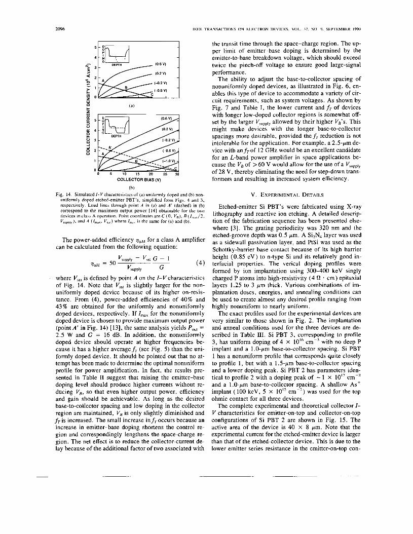
To determine the effect of nonuniform doping profiles on large-signal performance, a simple class A power anal- ysis following the methods of Kushner [12] was per- formed for profiles 1 and 3 . The I-V characteristics and doping profiles of Figs. 3 and 4 are combined in Fig. 14, together with the assumed load lines. The maximum col- lector voltage (point C in Fig. 14) of the two devices is limited by avalanche breakdown to 20 V for the uniformly doped device and 30 V for the nonuniformly doped de- vice. This, in turn, limits the supply voltage (point B in Fig. 14) of the uniformly and nonuniformly doped de- vices to 10 and 15 V, respectively. The maximum collec- tor current I,,, (point A in Fig. 14) is chosen to maximize the output power Pout for the uniformly doped device, and the identical I,,, is chosen for the nonuniformly doped device to simplify the comparison. Assuming a device ac- tive area of 4.6 x cm2 (I , , , = 0.6 A), output pow- ers of 2.25 and 1.5 W for the nonuniformly and uniformly doped devices, respectively, were obtained. The input power Pin required to produce these output powers is re- lated to the base-voltage swing and average input capac- itance along the load lines indicated in Fig. 14. The smaller base-voltage swing for the uniformly doped de- vice is somewhat offset by its larger average input capac- itance, so the input levels for both devices are within ap- proximately 5% of each other. The lower average input capacitance associated with the nonuniformly doped de- vice is consistent with the fact that fT remains high over its entire voltage range (see Fig. 5) . If the uniformly doped device is assumed to have a large-signal gain G( = Pout/Pin) of 14 dB, which is typical for these devices at L-band frequencies, then G calculated for the nonuni- formly doped device is approximately 15.7 dB. Note that the nonuniformly doped device has a larger G despite its higher output conductance. This is due to the larger Pout achievable with the nonuniformly doped device and is in contrast to the lower maximum small-signal gain one might expect for a device with higher output conductance.
2096 IEEE TRANSACTIONS ON ELECTRON DEVICES. VOL. 37. NO 9. SEPTEMBER 1990
(0.6 V)
(0.2 V)
(-0.2 V)
(-0.6 V)
I
COLLECTOR BIAS (V)
(b) Fig. 14. Simulated I - V characteristics of (a) uniformly doped and (b) non-
uniformly doped etched-emitter PBT’s, simplified from Figs. 4 and 3 , respectively. Load lines through point A in (a) and A’ (dashed) in (b) correspond to the maximum output power [ 141 obtainable for the two devices in class A operation. Point coordinates are C (0, V s ) , B ( I , , , , / 2 , V , . p p l y ) , and A ( I , , , , V , , , ) where I,,, is the same for (a) and (b).
The power-added efficiency 7,dd for a class A amplifier can be calculated from the following equation:
where V,,, is defined by point A on the I-V characteristics of Fig. 14. Note that VSat is slightly larger for the non- uniformly doped device because of its higher on-resis- tance. From (4), power-added efficiencies of 40% and 43% are obtained for the uniformly and nonuniformly doped devices, respectively. If I,,,,, for the nonuniformly doped device is chosen to provide maximum output power (point A’ in Fig. 14) [13], the same analysis yields Po,, = 2.5 W and G = 16 dB. In addition, the nonuniformly doped device should operate at higher frequencies be- cause it has a higher averagefT (see Fig. 5 ) than the uni- formly doped device. It should be pointed out that no at- tempt has been made to determine the optimal nonuniform profile for power amplification. In fact, the results pre- sented in Table I1 suggest that raising the emitter-base doping level should produce higher currents without re- ducing v,, so that even higher output power, efficiency and gain should be achievable. As long as the desired base-to-collector spacing and low doping in the collector region are maintained, VB is only slightly diminished and fT is increased. The small increase infT occurs because an increase in emitter-base doping shortens the control re- gion and correspondingly lengthens the space-charge re- gion. The net effect is to reduce the collector-current de- lay because of the additional factor of two associated with
the transit time through the space-charge region. The up- per limit of emitter-base doping is determined by the emitter-to-base breakdown voltage, which should exceed twice the pinch-off voltage to ensure good large-signal performance.
The ability to adjust the base-to-collector spacing of nonuniformly doped devices, as illustrated in Fig. 6, en- ables this type of device to accommodate a variety of cir- cuit requirements, such as system voltages. As shown by Fig. 7 and Table I, the lower current and fT of devices with longer low-doped collector regions is somewhat off- set by the larger Vsupply allowed by their higher V,’S. This might make devices with the longer base-to-collector spacings more desirable, provided the fT reduction is not intolerable for the application. For example, a 2.5-pm de- vice with anfTof 12 GHz would be an excellent candidate for an L-band power amplifier in space applications be- cause the VB of > 60 V would allow for the use of a Vsupply of 28 V, thereby eliminating the need for step-down trans- formers and resulting in increased system efficiency.
V. EXPERIMENTAL DETAILS
Etched-emitter Si PBT’s were fabricated using X-ray lithography and reactive ion etching. A detailed descrip- tion of the fabrication sequence has been presented else- where [3]. The grating periodicity was 320 nm and the etched-groove depth was 0.5 pm. A Si3N4 layer was used as a sidewall passivation layer, and PtSi was used as the Schottky-barrier base contact because of its high barrier height (0.85 eV ) to n-type Si and its relatively good in- terfacial properties. The verical doping profiles were formed by ion implantation using 300-400 keV singly charged P atoms into high-resistivity ( 4 !J cm) epitaxial layers 1.25 to 3 pm thick. Various combinations of im- plantation doses, energies, and annealing conditions can be used to create almost any desired profile ranging from highly nonuniform to nearly uniform.
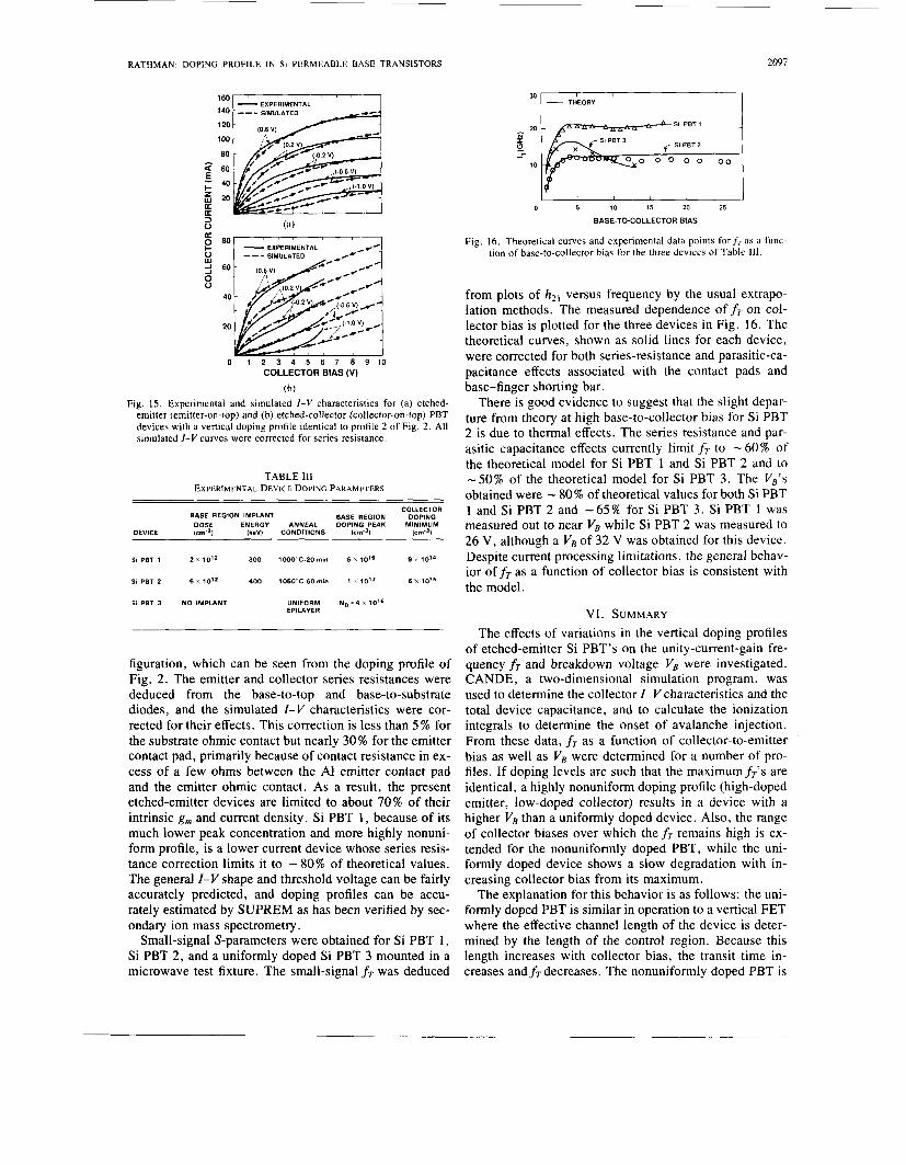
The exact profiles used for the experimental devices are very similar to those shown in Fig. 2. The implantation and anneal conditions used for the three devices are de- scribed in Table 111. Si PBT 3, corresponding to profile 3 , has uniform doping of 4 x 10l6 cmP3 with no deep P implant and a 1.0-pm base-to-collector spacing. Si PBT 1 has a nonuniform profile that corresponds quite closely to profile 1 , but with a 1 .5-pm base-to-collector spacing and a lower doping peak. Si PBT 2 has parameters iden- tical to profile 2 with a doping peak of - 1 X 10’’ cmP3 and a 1.0-pm base-to-collector spacing. A shallow As’ implant (100 keV, 5 X l O I 5 cm-2) was used for the top ohmic contact for all three devices.
The complete experimental and theoretical collector I- V characteristics for emitter-on-top and collector-on-top configurations of Si PBT 2 are shown in Fig. 15. The active area of the device is 40 X 8 pm. Note that the experimental current for the etched-emitter device is larger than that of the etched-collector device. This is due to the lower emitter series resistance in the emitter-on-top con-
RATHMAN: DOPING PROFILE IN Si PERMEABLE BASE TRANSlSTORS 2097
I I I I I - THEORY 30
0 5 10 15 20 25
BASE-TO-COLLECTOR BIAS
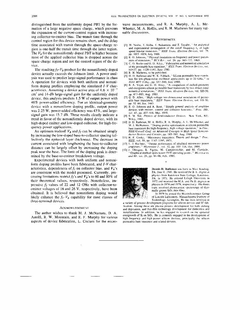
Fig. 16. Theoretical curves and experimental data points forfr as a func- tion of base-to-collector bias for the three devices of Table 111.
from plots of h2, versus frequency by the usual extrapo- lation methods. The measured dependence of fr on col- lector bias is plotted for the three devices in Fig. 16. The theoretical curves, shown as solid lines for each device,
0 1 2 3 4 5 6 7 6 9 1 0 were corrected for both series-resistance and parasitic-ca- pacitance effects associated with the contact pads and COLLECTOR BIAS (V)
(b) Fig. 15. Experimental and simulated I-V characteristics for (a) etched-
emitter (emitter-on-top) and (b) etched-collector (collector-on-top) PBT devices with a vertical doping profile identical to profile 2 of Fig. 2. All simulated I-V curves were corrected for series resistance.
TABLE 111 EXPERIMENTAL DEVICE DOPING PARAMETERS
COLLECTOR EASE REGION IMPLANT EASE REGION DOPING
DOSE ENERGY ANNEAL DOPING PEAK MINIMUM DEVICE bd) IkeVI CONDITIONS ( ~ r n - ~ l icm-3i
SI PET 1 2 x 10l2 300 lOOO"C-20m1n 6 X 10l6 9 x 1 0 1 ~
SI PET 2 6 X 10l2 400 1050°C-60 mm 1 X lo1' 6 X 10¹⁵
51 PET 3 NO IMPLANT UNIFORM ND = 4 X 10l6 EPIlAYER
figuration, which can be seen from the doping profile of Fig. 2. The emitter and collector series resistances were deduced from the base-to-top and base-to-substrate diodes, and the simulated I-V characteristics were cor- rected for their effects. This correction is less than 5 % for the substrate ohmic contact but nearly 30% for the emitter contact pad, primarily because of contact resistance in ex- cess of a few ohms between the A1 emitter contact pad and the emitter ohmic contact. As a result, the present etched-emitter devices are limited to about 70% of their intrinsic g,,, and current density. Si PBT 1 , because of its much lower peak concentration and more highly nonuni- form profile, is a lower current device whose series resis- tance correction limits it to - 80% of theoretical values. The general I-V shape and threshold voltage can be fairly accurately predicted, and doping profiles can be accu- rately estimated by SUPREM as has been verified by sec- ondary ion mass spectrometry.
Small-signal S-parameters were obtained for Si PBT 1, Si PBT 2, and a uniformly doped Si PBT 3 mounted in a microwave test fixture. The small-signal fT was deduced
base-finger shorting bar. There is good evidence to suggest that the slight depar-
ture from theory at high base-to-collector bias for Si PBT 2 is due to thermal effects. The series resistance and par- asitic capacitance effects currently limit fr to - 60% of the theoretical model for Si PBT 1 and Si PBT 2 and to -50% of the theoretical model for Si PBT 3 . The VB's obtained were - 80% of theoretical values for both Si PBT 1 and Si PBT 2 and -65% for Si PBT 3. Si PBT 1 was measured out to near V, while Si PBT 2 was measured to 26 V, although a V, of 32 V was obtained for this device. Despite current processing limitations, the general behav- ior offT as a function of collector bias is consistent with the model.
VI. SUMMARY The effects of variations in the vertical doping profiles
of etched-emitter Si PBT's on the unity-current-gain fre- quency fT and breakdown voltage V, were investigated. CANDE, a two-dimensional simulation program, was used to determine the collector I- V characteristics and the total device capacitance, and to calculate the ionization integrals to determine the onset of avalanche injection. From these data, fr as a function of collector-to-emitter bias as well as V, were determined for a number of pro- files. If doping levels are such that the maximumfr's are identical, a highly nonuniform doping profile (high-doped emitter, low-doped collector) results in a device with a higher V, than a uniformly doped device. Also, the range of collector biases over which the fT remains high is ex- tended for the nonuniformly doped PBT, while the uni- formly doped device shows a slow degradation with in- creasing collector bias from its maximum.
The explanation for this behavior is as follows: the uni- formly doped PBT is similar in operation to a vertical FET where the effective channel length of the device is deter- mined by the length of the control region. Because this length increases with collector bias, the transit time in- creases and fT decreases. The nonuniformly doped PBT is
2098 IEEE TRANSACTIONS ON ELECTRON DEVICES, VOL. 37. NO. 9. SEPTEMBER 1990
distinguished from the uniformly doped PBT by the for- mation of a large negative space charge, which prevents the expansion of the current-control region with increas- ing collector-to-emitter bias. The transit time through the control region for this device remains short, and the delay time associated with transit through the space-charge re- gion is one-half the transit time through the latter region. The VB for the nonuniformly doped PBT is higher because most of the applied collector bias is dropped across the space-charge region and not the control region of the de- vice.
The resultingfTVB product for the nonuniformly doped device actually exceeds the Johnson limit. A power anal- ysis was used to predict large-signal performance in class A operation for devices with both uniform and nonuni- form doping profiles employing the simulated I- I/ char- acteristics. Assuming a device active area of 4.6 x cm2 and 14-dB large-signal gain for the uniformly doped device, this analysis predicts 1.5 W of output power with 40 % power-added efficiency. For an identical-geometry device with a nonuniform doping profile, output power was 2.25 W, power-added efficiency was 43 % , and large- signal gain was 15.7 dB. These results clearly indicate a trend in favor of the nonuniformly doped device, with its high-doped emitter and low-doped collector, for high-fre- quency power applications.
An optimum tradeoff VB andfT can be obtained simply by increasing the low-doped base-to-collector spacing (ef- fectively the epitaxial layer thickness). The decrease in current associated with lengthening the base-to-collector distance can be largely offset by increasing the doping peak near the base. The limit of the doping peak is deter- mined by the base-to-emitter breakdown voltage.
Experimental devices with both uniform and nonuni- form doping profiles have been fabricated, and I-I/ char- acteristics, dependences of fT on collector bias, and VB’s are consistent with the model presented. Currently, pro- cessing limitations restrictfr‘s and ve’s to 60 and 80% of their theoretical values, respectively. Nonetheless, im- pressive fT values of 22 and 12 GHz with collector-to- emitter voltages of 16 and 26 V, respectively, have been obtained. It is believed that nonuniform doping would likely enhance the frVB capability for most classes of three-terminal devices.
ACKNOWLEDGMENT The author wishes to thank M. J. McNamara, D. A.
Astolfi, R. W. Mountain, and R. F. Murphy for various aspects of device fabrication, L. Cociani for the micro-
wave measurements, and R. A. Murphy, A. L. Mc- Whorter, M. A. Hollis, and R. H . Mathews for many val- uable discussions.
REFERENCES [ I ] M. Nanba, T. Shiba, T. Nakamura, and T. Toyabe, “An analytical
and experimental investigation of the cutoff frequency fT of high- speed-bipolar transistors,” IEEE Trans. Electron Devices, vol. 35 , pp. 1021-1028, July 1988.
[2] E. 0. Johnson, “Physical limitations on frequency and power param- eters of transistors,” RCA Rev., vol. 26, pp. 163-177, 1965.
[3] C. 0. Bozler and G . D. Alley, “Fabrication and numerical simulation of the permeable base transistor,” IEEE Trans. Elecrron Devices, vol. ED-27, pp. 1128-1 141, June 1980.
[4] R. H. Mathews, to be published. [5] D. D. Rathman and W. K. Niblack, “Silicon permeable base transis-
tors for low-phase-noise oscillator applications up to 20 GHz,” in lEEE MTT-S Dig., pp. 537-540, June 1980.
[6] B. A. Vojak and G . D. Alley, “A comparison of etched-geometry and overgrown silicon permeable base transistors by two-dimensional numerical simulations,” IEEE Trans. Electron Devices, vol. ED-30,
[7] G. D. Alley, “High-voltage two-dimensional simulations of perme- pp. 877-883, Aug. 1983.
able base t;ansistok,” IEEE Trans. Electron Devices, vol. ED-30, pp. 52-60, Jan. 1983. E. 0. Johnson and A. Rose, “Simple general analysis of amplifier devices with emitter, control and collector functions,” Proc. IRE, vol. 47, pp. 407-418, Mar. 1959. S . M. Sze, Physics of Semiconductor Devices. New York, N Y : Wiley, 1981. D. D. Rathman, M. A. Hollis, R. A. Murphy, A. L. McWhorter, and M. J. McNamara, “Doping profile optimization in silicon permeable base transistors for high-frequency, high-voltage operation,” in Proc. IEEEICornell Con$ on Advanced Concepts in High Speed Semicon- ducror Devices und Circuits, pp. 185-193, Aug. 1989. H. F. Cooke, “Microwave transistors: Theory and design,” Proc. IEEE, vol. 59, pp. 1163-1195, 1971. L. J. Kushner, “Output performance of idealized microwave power amplifiers,” Microwave J . , vol. 32 , pp. 103-116, Oct. 1989. J . Obregon, E. Ngoya, M. Campovecchio, and M. Camiade, “Graphical method spots power-FET operating points, ’‘ Microwaves and RF, vol. 28, pp. 91-96, Feb. 1989.
*
Dennis D. Rathman was born in West Reading, PA, June 8, 1949. He received the B . A . degree in physics from Kutztown State College, Kutztown, PA, in 1971. He entered Lehigh University in 1972 and received the M.S. and Ph.D. degrees in physics in 1974 and 1979, respectively. His thesis topic involved photocurrent spectrocopy of ther- mally grown SiOz thin films.
In 1979 he joined the Microelectronics Group of Lincoln Laboratory, Massachusetts Institute of Technology, Lexington. He has been involved in
a variety of process development programs for silicon devices and IC fab- rication. Among these are plasma process development for both etching and deposition, and thin-film technology development for dielectrics and metallizations. In addition, he has engaged in research on the epitaxial overgrowth of Si on SiOz. He is currently engaged in the development of high-frequency and-high-power silicon devices, principally the silicon permeable base transistor and related devices.